development and application of magneto-optical …home.sato-gallery.com/research/nmm2008.pdf · in...
TRANSCRIPT

Development and Application of Magneto-Optical Microscope Using Polarization-Modulation Technique
K. Sato (Tokyo Univ. Agric. & Tech/JST)T. Ishibashi (Nagaoka Univ. Technology)
NMM2008, Okinawa

Outline
1. Introduction2. MO imaging using polarization modulation
technique3. MO indicator film
Bi:YIG by MOD method4. Magnetic imaging
1. Patterned MgB2 film2. Magnetic nanostructures
5. Summary

1. Introduction

Magnetic Imaging using MO method
Magneto-optical (MO) microscopes have been used as one of the most significant techniques for an observation of magnetic domain structures in magnetic materials. Recently, this technique attracts great attention as a powerful tool for visualization of invisible phenomena: e.g.,
spin-accumulation in nonmagnetic semiconductors (1,2)magnetic flux intrusion in superconductors (3)-(5) .
(1) S. A. Crooker et al.: Science, Vol.309, pp.2191-2195 (2005).(2) M. Yamanouchiet al.: Lett. Nature, Vol.428, pp.539-542 (2004).(3) S. Gotoh et al.: Jpn. J. Appl. Phys., Vo.29, L1083-L1085 (1990).(4) M. V. Indenbom et al.: Physica C, Vol.166, pp.486-496 (1990).(5) P.E. Goa et al.: Rev. Sci. Instrum., Vol.74, pp. 141-146 (2003).

Magnetic Garnet indicator film
Light
Magnetic Imaging of stray magnetic field using MO method
Stray field from sample magnetize the garnet film locally, and the distribution of field can be detected by means of MO method, as a polarization image.
Sample
Mirror layer
GGG substrate
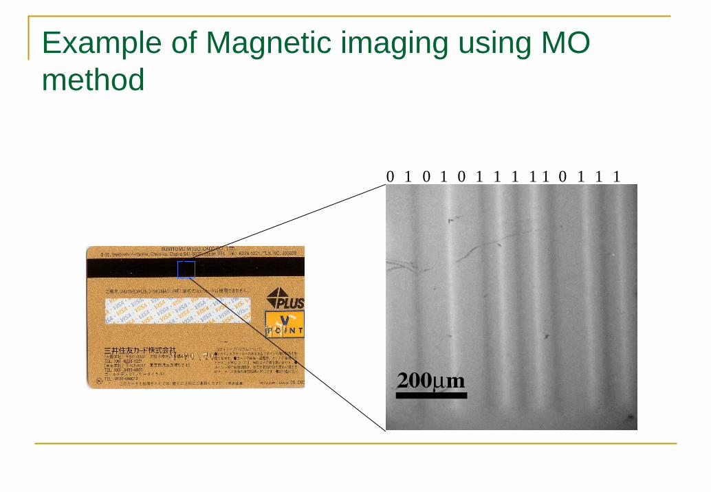
Example of Magnetic imaging using MO method
1 1 11 1 1 1 1 1 10 0 00

Advantages of MO imaging to other imaging techniques
MO microscopes have technical advantages:a short measuring timea simple instrumental setup compared with other imaging techniques, e.g., a magnetic force microscope (MFM) (6), a superconducting quantum interference device (SQUID) microscope (7) and a Hall-probe microscope (8).

Magnetic Imaging
MO microscope has advantages shown above.In addition, it is easy to develop it with low temperature, magnetic field, etc,since the MO microscope is a simple technique based on optical microscope.
QuantitativeMagnteic
measurement
SpatialResolution
Dynamicmeasurement
Measuring timefor one image
Special sampletreatment
Scanning SQUIDmicroscope
○:10-7T > 1 μm no > 1 min no
Scanning TunnelingMicroscope (STM)
× < 1 nm no > 1 minSurfacetreatment
(cleavage,etc.)
Magnetic ForceMicroscope (MFM)
△ < 10 nm no > 1 min no
Bitter Method × < 10 nm no ~10 msecDeposition of
magneticmaterials
Lorenz Microscope ○ < 1 μm yes ~10 msecThinner the
sample for TEMmeasurement
Magneto-OpticalMicroscope
○:10-5T < 1 μm yes ~10 msec no

Conventional MO microscope
analyzer
polarizer
Objective lens sample
electromagnet
Light source
CCD camera
Slightly off (~4 deg) from cross-polarizer configuration
B
P
A
L
D
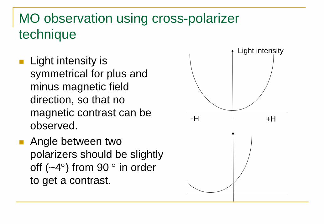
MO observation using cross-polarizer technique
Light intensity is symmetrical for plus and minus magnetic field direction, so that no magnetic contrast can be observed. Angle between two polarizers should be slightly off (~4°) from 90 ° in order to get a contrast.
+H-H
Light intensity

Problems in MO imaging
Image is dark. Quantitative measurement of MO values, Faraday effect, Kerr effect in inhomogeneous samples is difficult.
Zigzag Domain structure in MO indicator film deteriorates images.
MO microscope using polarization modulation technique.
Bi:YIG prepared by metal-organic decomposition method.

2. MO microscope using polarization modulation method

Polarization modulation technique using photoelastic modulator (PEM)
Magneto-optical spectra have been measured using PEM which modulates retardation of light at p rad/s to produce LP, LCP and RCP sequentially.Polarization rotation is given by detecting 2p component and ellipticity is given by p component.

Retardation modulation using PEMP and A are linear polarizers,M photoelastic modulator(PEM),D a detector.PEM consists of an isotropic transparent material (quartz,CaF2 etc.) and a piezoelectric vibrator made of quartz.If PEM is fed with HF electric field with angular frequency of p[rad/s] , standing wave of the acoustic sound which generates in the transparent material uniaxial anisotropy oscillating with angular frequency p [rad/s, which in turn leads to appearance of Δn.Optical retardation δ=Δnl/λ is modulated with an angular frequency of p [rad/s], therefore
δ=δ0sinpt .
i
j
π/4
P
PEM
AD
quartz Isotropicmaterial
B
Fused silica CaF2Ge etc..
piezoelectric
amplitude
position
l
Optical retardationδ=(2π/λ)Δnl sin pt =δ0sin ptΔn=ny-nx
x
y

Scematic explanation of retardation modulation •Fig.(a) shows time-variation of optical retardation δ
If the amplitude δ 0 takes a value π/2, positive and negative peaks of δ correspond to RCP (right circularly polarized light) and LCP (left circularly polarized light), respectively. •If the sample shows neither rotation nor circular dichroism, the lotus of the detected electric field vector changes as LP-RCP-LP-LCP-LP, as shown in Fig.(b).The x-component does not change as shown in Fig. (c).•If the sample show rotation, the lotus varies as shown in Fig. (d) and the x-component oscillates with angular frequency of 2p as illustrated in Fig.(e).•If circular dichroism exists vector length of RCP and LCP becomes different as shown in Fig. (f), leading to oscillation of x-component with angular frequency of p[rad/s].

L MC
P
A
C (f Hz)
M1
M2
PEM(p Hz) S
Electromagnet
D
Preamplifier
LA1 (f Hz)
LA2 (p Hz)
LA3 (2p Hz)
MO Spectrometer layout

Magneto-optical spectrometer
Xe lamp
Double monochromator
Optical system Electromagnet
Sample
Lockin amplifier Lockin amplifier 2
Power supplyfor electromagnet
Preamplifier
Power sourcefor Xe lamp
Wavelengthscan driver
PEM controler

How to apply modulation technique to MO microscopy
Conventional PEM employs a modulation frequency as high as 50 KHz, which exceeds the frame rate of CCD cameras and cannot be directly applicable to MO microscopy.In the retardation modulation technique, rotation produces difference in x-component of linear polarization (LP) and circular polarization (CP), while circular dichroism (=ellipticity) produces difference in the x-component of right circular and left circular polarizations
Rotation producesdifference between LP and CP
Circular dichroism producesdifference between RCP and LCP

Modulation technique using image processing
It is thus elucidated as follows:MO rotation image can be obtained by an image processing to take difference between LP and CP images.MO ellipticity image can be obtained by an image processing to take difference between RCP and LCP images.

Novel MO microscope with retardation modulation
Microscope: Olympus BH-UMA CCD camera:Hamamatsu C4880 (Cooled)Analyzer(fixed): Glan-Thomson MG*B10Objective lens: NeoSPlanNIC 10 × 50Rotatable quarter waveplate:ACP-400-700
(acromatic waveplate)Polarizer(fixed):Glan-Thomson (MG*B10)Bandpass filter: Interference filter
(450, 500,550, 600, 650 nm, BW=10nm) Light source: Halogen-tungsten lamp 20W

Principle of image processing
E2 = ASQPE1
=12
1 11 1
⎛
⎝ ⎜
⎞
⎠ ⎟
cosθF + iηF sinθF −sinθF + iηF cosθF
sinθF − iηF cosθF cosθF + iηF sinθF
⎛
⎝ ⎜
⎞
⎠ ⎟
1+ icos2ϕ isin2ϕisin2ϕ 1− icos2ϕ
⎛
⎝ ⎜
⎞
⎠ ⎟
1 00 0
⎛
⎝ ⎜
⎞
⎠ ⎟
Ex
Ey
⎛
⎝ ⎜
⎞
⎠ ⎟
=12
cosθF + sinθF −ηF sin 2ϕ + θF( )− cos 2ϕ + θF( )( )+ i cos 2ϕ + θF( )+ sin 2ϕ + θF( )+ ηF sinθF − cosθF( ){ }cosθF + sinθF −ηF sin 2ϕ + θF( )− cos 2ϕ + θF( )( )+ i cos 2ϕ + θF( )+ sin 2ϕ + θF( )+ ηF sinθF − cosθF( ){ }
⎛
⎝ ⎜ ⎜
⎞
⎠ ⎟ ⎟ Ex
I ϕ( )= cosθF + sinθF −ηF sin 2ϕ + θF( )− cos 2ϕ + θF( )( )( )2
+ cos 2ϕ + θF( )+ sin 2ϕ + θF( )+ ηF sinθF − cosθF( )( )2Ex
2 /4
H
αE1 E2 E3E4
PolarizerSampleRotation θF
Elipticity ηF
λ/4Wave plate Analizer
CCDcamera
I(0º)I(45º)I(−45º)
ψ= 0º LP45º RCP-45 º LCP
ψ = 45ºψ = -45ºψ = 0 α = 45º
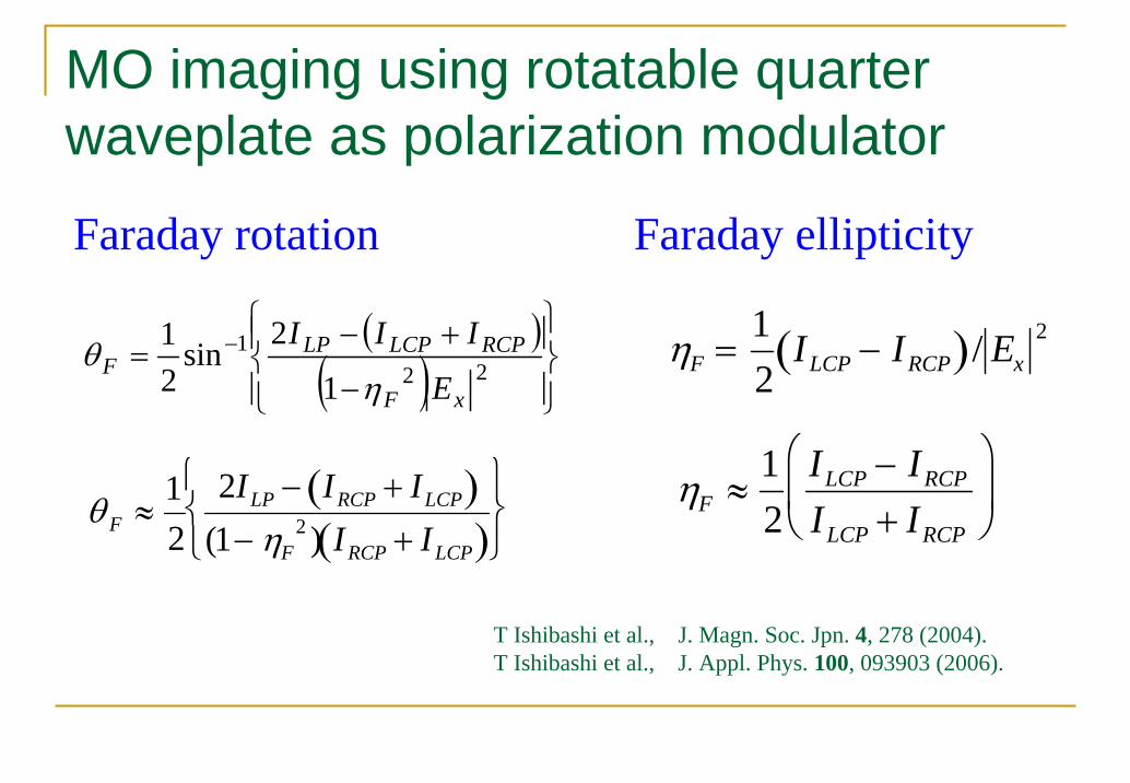
MO imaging using rotatable quarter waveplate as polarization modulator
T Ishibashi et al., J. Magn. Soc. Jpn. 4, 278 (2004).T Ishibashi et al., J. Appl. Phys. 100, 093903 (2006).
Faraday rotation Faraday ellipticity
( )( ) ⎪⎭
⎪⎬⎫
⎪⎩
⎪⎨⎧
−
+−= −
221
1
2sin
21
xF
RCPLCPLPF
E
III
ηθ ηF =
12
ILCP − IRCP( )/ Ex2
θ F ≈12
2ILP − IRCP + ILCP( )(1− ηF
2 ) IRCP + ILCP( )⎧ ⎨ ⎩
⎫ ⎬ ⎭
ηF ≈12
ILCP − IRCP
ILCP + IRCP
⎛
⎝ ⎜
⎞
⎠ ⎟

θF =12
sin−1 −2I(0) − I(π /4) + I(−π /4){ }
(1−ηF2) Ex
2
⎧ ⎨ ⎪
⎩ ⎪
⎫ ⎬ ⎪
⎭ ⎪
CCD image (a) LP, (b) RCP, (c) LCP, Processed image (d) rotation (e) ellipticityηF ≈ −
12
I(π /4) − I(−π /4)I(π /4) + I(−π /4)
⎧ ⎨ ⎩
⎫ ⎬ ⎭
Faraday rotation
Faraday ellipticity100 μm
ηF = −12
Evaluation of Faraday rotation
I(π /4) − I(−π /4){ }/ Ex2
θF ≈12
2I(0) − I(π /4) + I(−π /4)[ ](1−ηF
2) I(π /4) + I(−π /4)[ ]⎧ ⎨ ⎩
⎫ ⎬ ⎭ ηF
θF

SampleY2BiFe4GaO12 Film/glass sub.prepared by MOD method
Rectangular Dots arraySize 50μm×50μmThickness 200nm
An optical microscope image
T. Ishibashi et al, J. Appl. Phys., 97, 013516 (2005).
Transmittances of glass substrate and garnet dot are quite different.It is hard to obtain quantitative magnetic contrast by conventional MO imaging technique.

Image of Faraday Rotation
Reversal of magnetic contrast corresponding to magnetization reversal
Mag
netic
fiel
d re
vers
al.
Image of Faraday ellipticity
λ=500 nm

Quantitative evaluation.
Rotation angle is obtained quantitatively.
Magnetization reversal λ=500 nm
-1
-0.5
0
0.5
1
500 600 700 800 900 1000
Far
aday
Rota
tion (de
gree)
Position (pixel)
-1
-0.5
0
0.5
1
500 600 700 800 900 1000
Far
aday
Rota
tion (de
gree)
Position (pixel)

Hysteresis measurement
Magnetic field dependences of patterned garnet film measured with wavelength of 500 nm. Clear hysteresis loop was observed at garnet dot although no signal was obtained at glass substrate. Hysteresis data can be obtained for each pixels.
λ=500 nm

Averaging and smoothing
-0.4
-0.2
0
0.2
0.4
500 600 700 800 900 1000
Far
aday
Rota
tion
(deg
ree)
Position (pixel)
σ = 0.470º
-0.4
-0.2
0
0.2
0.4
500 600 700 800 900 1000
Far
aday
Rota
tion (de
gree)
Position (pixel)
σ = 0.148º
-0.4
-0.2
0
0.2
0.4
500 600 700 800 900 1000
Far
aday
Rota
tion (de
gree)
Position (pixel)
σ = 0.046º
σ : standard deviation
1 shotσ=0.920º
10 times accumulationσ= 0.148º
10 times accumulation+ smoothing
σ= 0.048º

Faraday rotation and Faraday ellipticity spectra of patterned garnet film using MO microscope
Dots show data measured by MO microscope using interference filter(450, 500,550, 600, 650 nm) with band width of 10nm. Solid lines show spectra measured by MO spectrometer for garnet film without pattering.
-5
-4
-3
-2
-1
0
400 500 600 700
Fara
day
rota
tion
(104 d
egre
e/cm
)
Wavelength (nm)
θF of YBFG thin film
by MO spectrometer
θF of patterned YBFG
by MO microscope
0
1
2
3
4
5
6
7
400 500 600 700
Fara
day
ellip
ticity
(104 d
egre
e/cm
)
Wavelength (nm)
Faraday rotation Faraday ellipticity

The merits of the method
MeritsSimultaneous measurement of rotation and ellipticity in one cycle of measurementQuantitative evaluation of rotation and ellipticity is possible (standard sample is not necessary)Faraday image can be clearly displayed even in the sample with inhomogeneous transmissionMagnetic hysteresis loops at any pixel point can be displayed, once MO images are acquired for a sequence of magnetic field swinging between negative and positive magnetic saturation.
DemeritThis method takes a few tens of second to get one MO image.

MO imaging using LCM as polarization modulator
T Ishibashi et al., J. Magn. Soc. Jpn. 4, 278 (2004).T Ishibashi et al., J. Appl. Phys. 100, 093903 (2006).
Liquid crystal: ZLI-4792Substrate: ITO coated glass
45¼
Light Source
Polarizer Analyzerλ/4 plate SampleθF, ηF
Image sensor
x
y
0¼ ϕ
0¼45¼
Light Source
Polarizer AnalyzerLCM
SampleθF, ηF Image sensor
x
y
45¼

MO microscope
CCD camera Hamamatsu C9300 201Number of Pixels 640×480Data transfer 150 frame/s
ComputerCPU XEON 3.2GHzRAM 2GB
Interface AD-DA, GPIB, etc.
Software DevelopmentVisual Basic 6.0, Image capture SDK
T ishibashi et al., JAP, 100, 093903 (2006).
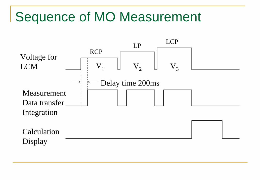
Voltage forLCM V1 V2 V3
MeasurementData transferIntegration
RCPLP LCP
CalculationDisplay
Delay time 200ms
Sequence of MO Measurement

0s 1s 2s 3s
4s 5s 6s 7s
8s 9s 10s 11s
Real time observation
Sample Y2BiFe4GaO12
Pattern size 50μm square

3. MO indicator film

Requirements for MO indicator
Large Faraday effectFor visualize magnetic field
Thin film with a thickness of ~ 1μmTo detect magnetic field near sample before its distribution smears out.
In-plane magnetization without magnetic domain For high resolution magnetic image

Problem with Domain StructureIf we use LPE garnet as an MO indicator, Zigzag-shaped magnetic domain appears in garnet film magnetized in-plane, which makes it difficult to observe a signal from a sample, especially in the case that a signal is small.
LPE grown garnet as indicator
Groove pattern
Nb film with groove pattern

MOD process
Cleaning of Substrates
Spin Coating
Drying
Pre annealing
Crystallization
Repeat 150℃ 5〜60min
450℃ 10min
550℃~900℃ 1h
Step1 500rpm 5sec
Step2 4000rpm 30sec
•MOD solutions (by Kojundo chemical lab.)made from carboxylic acids ~3 mol%
•Chemical compositions YBiFeO Y:Bi:Fe 2:1:5
•SabstrateGd3Ga5O12 (111)

MO indicator film
Magnetic field dependence of Faraday rotation
Y3-xBixFe5O12
Y2BiFe5O12/GGG(111)Thickness 400 nm)
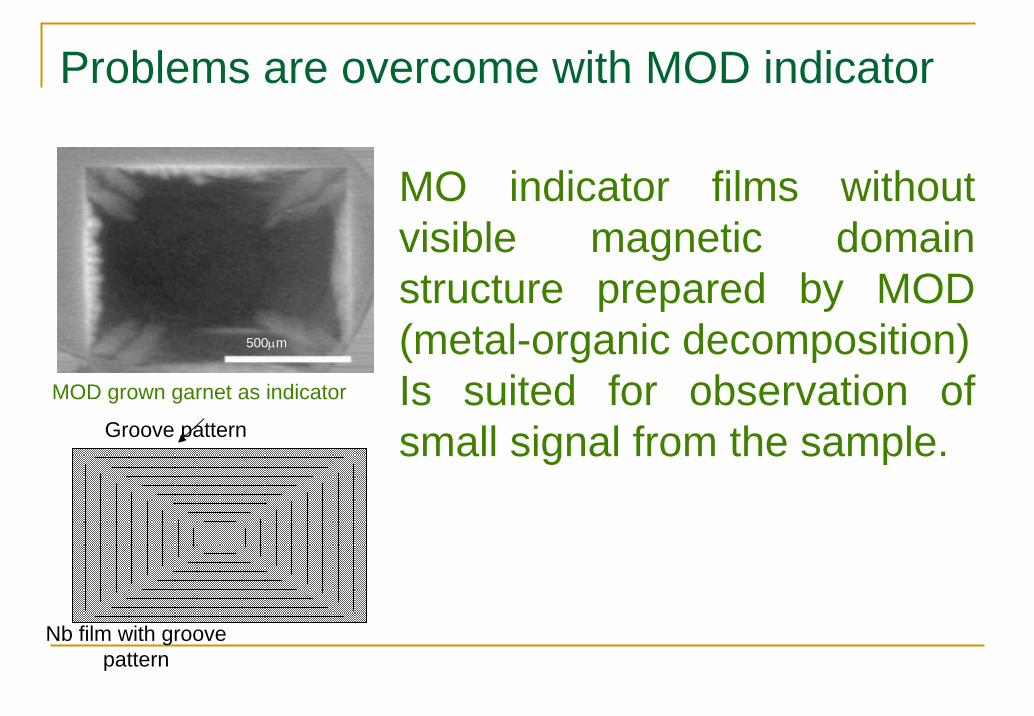
Problems are overcome with MOD indicator
Groove pattern
Nb film with groove pattern
MOD grown garnet as indicator
MO indicator films without visible magnetic domain structure prepared by MOD (metal-organic decomposition)Is suited for observation of small signal from the sample.
500μm500μm

4. Magnetic imaging (1) Superconducting film

Garnet film with Pt mirror
MgB2 pattern
Light
The magnetic flux intruding into the superconductor is transferred to the indicator film, The perpendicular component of the magnetization is observed by Faraday effect.
Magneto-optical image
PtMOD Bi:YIG, 400nm in thickness
Gd3Ga5O12 substrate
Al2O3substrate
MgB2
Prepared by MBEPatterned by photolithographythickness:100nmTc~30K
Sample setups

Square patternSize: 100μm×100μm
Patterned MgB2 film
100μm0.3 mm
Circle patternDiameter: 0.5mm
Optical images
Grown by NTT research lab.

0.3 mm 0.3 mm
Optical image (×5) of MgB2 pattern(0.5mm φ)
Optical image (×5) fromindicator
No direct optical image of MgB2 pattern is observed due to Pt mirror.
Only the magnetic fluxes can be visualized.
The image from the indicator side prevents direct optical image of circular dot due to Pt-mirror.

Optical image (×10) of MgB2square dots(100μm×100μm)
Optical image (×10) after stacking with
the indicator.
The image from the indicator side prevents direct optical image of square dots due to Pt-mirror.
100μm 100μm

24 Oe 46 Oe 123 Oe
735 Oe 368 Oe 0.1 Oe0.3 mm
MO images of 500μm circle
363 G0T = 3.9 K

24 Oe 46 Oe 123 Oe
735 Oe 0.1 Oe
0.3 mm
MO images showing intrusion of magnetic fluxes into an MgB2 circular dot at T=3.9K.
363 Oe0
磁力線
超伝導体superconductor
368 Oe
超伝導体
磁力線
superconductor

25 Oe 121 Oe 270 Oe
735 Oe 244 Oe -0.1 Oe
272 G0
MO images of 100μm square
100μm
T=3.9KT=3.9K

Magnetic image
Quantitative magnetic image can be obtained from MO image by using linear relation θF- B for the MO indicator film. Therefore, contrast in the image directly shows a magnetic field, B.
Magnetic image of remanent state after application of Magnetic field of 735 Oe.

MO image of MgB2
Z. X. Ye et al., APL 85 (2004) 5284.PLD-grownMgB2
MBE-grownMgB2
Oslo University
Present work

How to obtain current distributionfrom MO images
Biot-Savart’s law
Bz = μ0
4π(y − ′ y )Jx − (x − ′ x )Jy
r − ′ r 3∫ d ′ x d ′ y
Ampére’s law Ampére’s law
μ0J = Δ × BIt needs all B component, Bx, By, Bz, while MO images measures only Bz.
1) One uses models for current distribution and compare the calculated B with the measured one.
2) One directly inverts by numerical method.

Inversion of Biot-Savart’s law using convolution theorem
Bz = μ0H ex + μ0 K g (r, ′ r )g(x, y)d 3 ′ r V∫
g
B
K
g : local magnetizaionKg : green function
˜ B z(k) = μ0˜ K g (k) ˜ g (k)
Ch. Jooss et al. Physica C,299(1998)215.
z component of magnetic dipole
… (1)
Using convolution theoremEq.(1) can be transformed into
˜ j x = -i˜ B z˜ K x
˜ j x = - ˜ j xkx
ky˜ K x = μ0
e-kh
ksinh kd
2⎛ ⎝ ⎜
⎞ ⎠ ⎟
ky
k+
kx2
kyk
⎡
⎣ ⎢
⎤
⎦ ⎥
x and y component of J are obtained as Δ ⋅ J = 0

Density of lines corresponds to current density. Color indicates local moment obtained in a calculation.
Current density ~ 6×10⁷A/cm2
Magnetic & Current images

Nb pattern prepared on Bi:YIG
Substrate Gd3Ga5O12(111)MO indicator filmY2BiFe5O12 (400nm)
by MOD mothodSuperconductorNb (150nm)
by sputtering methodMirror Au Pattern size of anti-dots7, 10, 15μm□
Optical image

44 Oe 100 Oe 151 Oe 360 Oe 502 Oe
4 Oe 40 Oe 101 Oe 151 Oe 347 Oe
MO images of Nb 10μm × 10μm anti-dots pattern with applying magnetic field. The sample was zero-field cooled down to 3.5K.
MO images of 10mm anti-dots

1
2 3
4
1
4
3
2
High resolution MO image

4. Magnetic imaging (2) Magnetic structures

Y-shaped patterns buried in Si
4 μm 4 μm
Linearly aligned
Honeycombaligned
0.9 μm
Ni80Fe20SiO2
Si
Cross sectional SEM image

05.07.27 05.12.05
NA=0.6 NA=0.85
MO Observation of Y-shaped patterns
5μmSEM image MFM image
MO images

Use of MO indicator for observation of in-plane magnetization

ConclusionsQuantitative magnetic imaging by the MO imaging technique using the polarization modulation technique combined with MO indicator films was developed. This technique allows us quantitative and nondestructive measurements for magnetic stray field as well as current distribution. Evaluations of stray field, current distribution were demonstrated for the superconducting MgB2patterned sample.

AcknowledgementThis work has been supported in part by the Grant-in-Aid for Scientific Research (No.16360003) from the Japan Society for Promotion of Science. We thank Dr. H. Shibata of NTT basic Research Laboratory and Prof. M. Naito of Tokyo Univ. of Agriculture and Technology for MgB2 sample. We also thank Prof. T. H. Johansen and Mr. J. I. Vestgården of Univ. of Oslo for calculation of current images.
Prof. T. H. Johansen Mr. J. I. VestgårdenProf. M. Naito