development of a microfluidic device for patterning
TRANSCRIPT

DEVELOPMENT OF A MICROFLUIDIC DEVICE FOR PATTERNING
MULTIPLE SPECIES BY SCANNING PROBE LITHOGRAPHY
A Thesis
by
JUAN ALBERTO RIVAS CARDONA
Submitted to the Office of Graduate Studies of
Texas A&M University
in partial fulfillment of the requirements for the degree of
MASTER OF SCIENCE
August 2006
Major Subject: Mechanical Engineering

DEVELOPMENT OF A MICROFLUIDIC DEVICE FOR PATTERNING
MULTIPLE SPECIES BY SCANNING PROBE LITHOGRAPHY
A Thesis
by
JUAN ALBERTO RIVAS CARDONA
Submitted to the Office of Graduate Studies of
Texas A&M University
in partial fulfillment of the requirements for the degree of
MASTER OF SCIENCE
Approved by:
Chair of Committee, Debjyoti Banerjee
Committee Members, Ali Beskok
Obdulia Ley
Jorge Seminario
Head of Department, Dennis O’Neal
August 2006
Major Subject: Mechanical Engineering

iii
ABSTRACT
Development of a Microfluidic Device for Patterning Multiple Species
by Scanning Probe Lithography. (August 2006)
Juan Alberto Rivas Cardona, B.S., Universidad de Guanajuato
Chair of Advisory Committee: Dr. Debjyoti Banerjee
Scanning Probe Lithography (SPL) is a versatile nanofabrication platform that leverages
microfluidic “ink” delivery systems with Scanning Probe Microscopy (SPM) for generating
surface-patterned chemical functionality on the sub-100 nm length scale. One of the prolific SPL
techniques is Dip Pen Nanolithography™ (DPN™). High resolution, multiplexed registration
and parallel direct-write capabilities make DPN (and other SPL techniques) a power tool for
applications that are envisioned in micro/nano-electronics, molecular electronics, catalysis,
cryptography (brand protection), combinatorial synthesis (nano-materials discovery and
characterization), biological recognition, genomics, and proteomics. One of the greatest
challenges for the successful performance of the DPN process is the delivery of multiple inks to
the scanning probe tips for nano-patterning. The purpose of the present work is to fabricate a
microfluidic ink delivery device (called “Centiwell”) for DPN (and other SPL) applications. The
device described in this study maximizes the number of chemical species (inks) for
nanofabrication that can be patterned simultaneously by DPN to conform the industrial standards
for fluid handling for biochemical assays (e.g., genomic and proteomic). Alternate applications
of Centiwell are also feasible for the various envisioned applications of DPN (and other SPL
techniques) that were listed above.

iv
The Centiwell consists of a two-dimensional array of 96 microwells that are bulk micromachined
on a silicon substrate. A thermoelectric module is attached to the back side of the silicon
substrate and is used to cool the silicon substrate to temperatures below the dew point. By
reducing the temperature of the substrate to below the dew point, water droplets are condensed in
the microwell array. Microbeads of a hygroscopic material (e.g., poly-ethylene glycol) are
dispensed into the microwells to prevent evaporation of the condensed water. Furthermore, since
poly-ethylene glycol (PEG) is water soluble, it forms a solution inside the microwells which is
subsequently used as the ink for the DPN process. The delivery of the ink to the scanning probe
tip is performed by dipping the tip (or multiple tips in an array) into the microwells containing
the PEG solution.
This thesis describes the various development steps for the Centiwell. These steps include the
mask design, the bulk micromachining processes explored for the micro-fabrication of the
microwell array, the thermal design calculations performed for the selection of the commercially
available thermoelectric coolers, the techniques explored for the synthesis of the PEG
microbeads, and the assembly of all the components for integration into a functional Centiwell.
Finally, the successful implementation of the Centiwell for nanolithography of PEG solutions is
also demonstrated.

v
To my dad and my sister because they are my source of inspiration,
and in loving memory of my dear mom.

vi
ACKNOWLEDGEMENTS
I would like to express my thankfulness to my advisor Dr. D. Banerjee for his trust, support, and
encouragement towards the achievement of this work. I have learned so much as a graduate
student while working under his supervision. I would also like to thank Dr. A. Beskok, Dr. J.
Seminario, and Dr. O. Ley for being part of my committee and assisting me when I needed help.
I gratefully acknowledge Dr. Cote for helpful suggestions about PEG-microbead synthesis. Also,
I would like to thank the current and former personnel of the Materials and Characterization
Facility, Yulia Vasileva (Research Assistant), Dr. William Lackowaski (former Manager),
Shyamashree Chaterjee (former Research Assistant), and Orla Wilson (Manager), who were
always willing to help me. I also acknowledge the support of CONACYT given through a
national scholarship.
Finally, I would like to express my deep appreciation for all those who have supported me in
either way (close or far away) through my time in College Station, especially my family and my
very good friends.

vii
TABLE OF CONTENTS
Page
ABSTRACT …………………………………………...……………………………..…… …….. iii
DEDICATION …………………………………………...…………………………..…… ……… v
ACKNOWLEDGEMENTS………………………………………...…………………..…..…….. vi
TABLE OF CONTENTS …………………………………………………...…………..… ……. vii
LIST OF FIGURES ………………………………………………………………….....… …….. ix
LIST OF TABLES ………………………………………………………………………... ……. xii
CHAPTER
I INTRODUCTION ………………………………………………………...... …….. 1
1.1 History of DPN …………………………………………………...…….. 1
1.2 The physics behind DPN ………………………………..….…… …….. 3
1.3 Applications for DPN…………………………….………..…….. …….. 8
1.4 Overview of the thesis …….…………………………..…..…….. ……. 11
II FABRICATION OF THE CENTIWELL MICROFLUIDIC INK
DELIVERY DEVICE………………………………………………………..
……. 13
2.1 Microfabrication processes ………………………..……………. ……. 13
2.2 Microfabrication of microwells for Centiwell device ……..……. ……. 19
2.3 Fabrication of PEG microbeads ……………………………..….. ……. 25
III EXPERIMENTAL APPARATUS AND TESTING OF THE CENTIWELL
MICROFLUIDIC INK DELIVERY DEVICE ………………………….…..
……. 33
3.1 Selection of the appropriate Peltier cooler ………..…………….. …… 34
3.2 Testing of the Centiwell microfluidic device ……..…………….. …… 42
3.3 Experimental apparatus …………………………………………. ……. 50

viii
CHAPTER Page
IV RESULTS …………………………………………………………..………. ……. 53
4.1 Condensation and “dipping” experiments ……..………………... ……. 53
4.2 DPN patterns …………………………………...………………...……. 57
V CONCLUSIONS ………………………………..………………………….. ……. 69
GLOSSARY ….…………………………………………………..…..…………………………. 71
REFERENCES …………………………………………………..…..…………………… ……. 73
APPENDIX A COMPUTER CODES …………………………..……………………… ……. 78
APPENDIX B SUPPLEMENTARY MATERIAL ……………..………………………. ……. 83
VITA …………………………………………………………….………………………………. 88

ix
LIST OF FIGURES
FIGURE Page
1.1 Dip Pen Nanolithography. A coated scanning probe moves across a surface
depositing “ink” molecules via the water meniscus …..………………….…….
……. 4
2.1 Photolithographic processes using both, positive and negative photoresist …….….. 16
2.2 Typical micro-fabrication process using the lift-off process ……………………….. 19
2.3 Photo-mask used for the photolithography process …………………………….….. 21
2.4 Schematic of the microwell fabrication process on silicon substrate ………….. ….. 22
2.5 96-microwell array obtained after the photolithography process and the
chromium deposition ………………………………………………………...…
….. 24
2.6 SEM picture of a microwell, (a) top view of the microwell, (b) tilted view of
the microwell obtained at a viewing angle of 30o …..……………………….....
….. 25
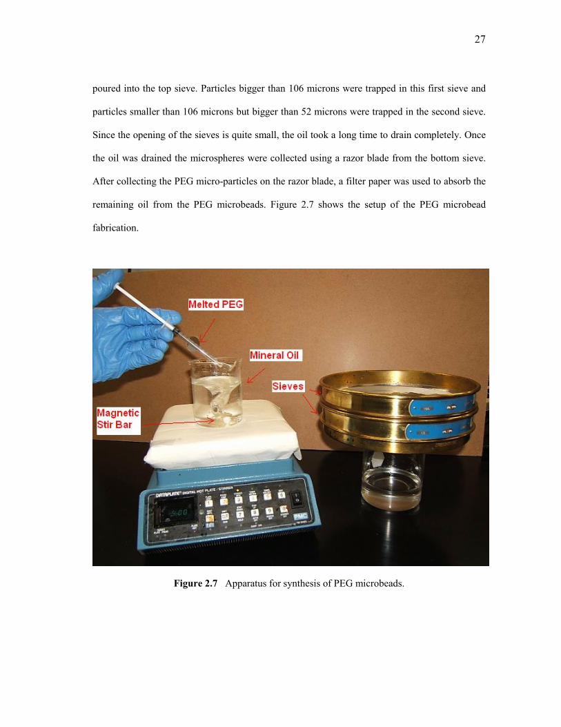
2.7 Apparatus for synthesis of PEG microbeads ……………………………………….. 27
2.8 PEG microbeads observed under a microscope……………………………..…..
….. 28
2.9 Flake-like microbeads synthesized in isopropyl alcohol ………………………..….. 29
2.10 PEG microbeads fabricated in isopropanol and functionalized with R6G
observed under a fluorescence microscope (Olympus BX61)……………..…
…… 30
2.11 PEG microbeads fabricated in pure mineral oil and functionalized with
Oregon Green 488X …………………………………………………….……..
….. 32
3.1 Schematic for design configuration of a Centiwell microfluidic ink delivery
device …………………………………………………………………..……....
….. 34
3.2 Sketch showing a Peltier cooler mounted on a heat sink to dissipate the heat
pumped from the object on the top …………………………………..………...
….. 35
3.3 Thermodynamic chart representing the procedure for obtaining the dew point
of a moist air mixture at State 1 ………………………………………..………
….. 37
3.4 Result from calculations for temperature profiles across the thickness of the
Centiwell substrate at different times ………………………………..………...
…… 40
x
FIGURE Page
3.5 Calculated values for heat load variation with respect to time for different
humidity ratios ……………………………………………………………..…..
….. 41
3.6 Sketch showing the shape of the TE-31-0.6-0.8 thermoelectric module …….... ...... 41
3.7 Sequence of images for several stages of condensation process on the
Centiwell without PEG microbeads……………………………………….…...
…… 45
3.8 Positioning of PEG microbeads into microwells using a micromanipulator…..
……. 46
3.9 Microwell array with PEG microbeads (fabricated using mineral oil) placed in
the microwells ………………………………………………………………....
…… 47
3.10 PEG microbeads fabricated using isopropanol and placed in microwells……..
…… 48
3.11 SEM image showing a section of the array ……………………………………
….. 49
3.12 Image from microscope showing condensed water droplets ………………..… ….. 50
3.13 Image showing PEG solutions in water trapped in the microwells while the
condensed water droplets on the surface have evaporated after disconnecting
power to the Peltier coolers …………………………………………………....
….. 50
3.14 Schematic for “dipping” experiments conducted by mounting the Centiwell
microfluidic device on an AFM stage………………………………………….
…… 52
4.1 Condensation on Centiwell substrate. Image shows water droplets merging
into the cavities at the location of the microwell array …………………….….
…… 54
4.2 PEG microbeads fabricated in isopropanol and placed inside
microwells...……………………………………………………………………
…… 56
4.3 Dipping process of the AFM tip.……………………………………………….
…… 57
4.4 Appearance of the PEG material inside the microwell at which the dipping
operation was performed ………………………………………………...…….
…… 58
4.5 Lateral force microscopy image of a set of three lines patterned with PEG by
DPN. Ambient humidity was recorded to be 60% …………………………….
…… 59
4.6 Discontinuous lines of PEG formed during patterning at a high speed using
the DPN process. The experiments were performed at an ambient humidity of
29% …………………………………………………………………………….
…… 61

xi
FIGURE Page
4.7 LFM images showing a set of three PEG lines patterned by DPN at an
ambient humidity of 65% ……………………………………………….……..
…… 63
4.8 Variation of line width for nano-patterned features of PEG versus writing
speed ………………………………………………...………………………....
....... 64
4.9 LFM image of the TAMU logo patterned with PEG by DPN ……………..…. …… 65
4.10 LFM images of the second TAMU logo patterned with the same PEG-coated
tip that generated the pattern in Figure 4.9 ……………….…………………....
……. 66
4.11 Height information of contact AFM showing fractal shapes formed during
DPN of PEG molecules on a mica substrate. The contact time of the scanning
probe tip on the mica surface was approximately 2 hours …..………………...
…… 68
B.1 Section analysis for the set of three lines shown in Figure 4.5. Ambient
humidity was recorded to be 60 % …………………………………………….
…… 83
B.2 Section analysis for the set of three discontinuous PEG lines shown in Figure
4.6. Experiment was carried out at an ambient humidity of 29% ………..……
…… 84
B.3 Section analysis for the set of three PEG lines patterned by DPN at an
ambient humidity of 65%. This pattern is shown in Figure 4.7……………..…
…… 85
B.4 Section analysis showing the different line widths found in the lithography of
the first TAMU logo ……………………………………………………...……
…… 86
B.5 Section analysis of the second TAMU logo shows slightly thinner PEG lines
than the ones obtained in the first TAMU pattern ……………………………..
….. 87

xii
LIST OF TABLES
TABLE Page
3.1 Dew point temperature for different relative humidities at an ambient
temperature of 25 oC …………………………………………………………..…
…… 36
3.2 Operation rating of the thermoelectric module TE-31-0.6-0.8 (Manufacturer: TE
Technology, Inc.) ………………………………………………………………...
….. 42

1
CHAPTER I
INTRODUCTION
Since ancient times, the ability to manipulate matter has been an endeavor for the human being.
Manipulation of matter in a desired and controlled way makes possible the performance of
nearly every engineered product. In 1959, a new concept for the manipulation, control and
organization of things at a very small scale (of the order of nanometers, 10-9m) was introduced
by the physicist Richard Feynman in his speech “There is plenty of room at the bottom.”1 The
concept, later named as Nanotechnology by Norio Taniguchi,2 comprised the possibility to
develop a method by which atoms and molecules could be manipulated individually.
1.1 History of DPN
Scanning Probe Microscopy (SPM) has been a key tool in monitoring and organizing matter on
the nanometer scale. SPM serves two important purposes. Scanning probes can be used to
monitor surface properties of various molecular phenomena as well as to manipulate molecules
on a surface. In the latter mode, the technique is often referred to as “Scanning Probe
Lithography” (SPL). Depending on the way the atoms or molecules are manipulated, SPL can be
classified in elimination lithography, addition lithography, or substitution lithography. One of the
most attractive modes of lithography for micro- and nano-fabrication is addition lithography,
since it allows the assembling of materials from the “bottom-up” rather than carving or etching
out patterns from bulk materials. However, manipulating materials as building blocks at the
nano-scale is not an easy task and research in this area of nanofabrication is at a stage of
exploration.
This thesis follows the style of Journal of Chemical Physics.

2
Early attempts to develop patterning methodologies from SPMs were able to demonstrate high-
resolution capabilities of these instruments. Scanning tunneling microscope (STM) based
methods either under ambient conditions3-7 or in ultrahigh vacuum (UHV)
8-12 as well as indirect
methods using atomic force microscope (AFM) for techniques such as “Nanografting” or
“Nanoshaving”13, 14
have been performed to obtain impressive high-resolution patterns.
However, these approaches are restricted by speed limitations and to only a few molecule-
substrate combinations.
Several other works have been performed on the patterning of self-assemble monolayers (SAM)
via addition using techniques other than scanning probes. These approaches, developed to
improve the resolution of techniques such as photolithography, include soft-lithography and
micro-contact printing15-18
as well as the incorporation of microfluidic devices for direct
patterning.19, 20
Lopez et al. created 50-micron wide lines of a C16S-SAM on gold using a
micropen,21 whereas Gaspar et al. patterned enzyme grids of 100-micron line width on gold
using a micro-dispenser.22 Deposition of different materials such as photoresist on gold
substrates,23 and DNA and proteins on glass,
24 were achieved by the use of nanopipettes. The
elaboration of these microfluidic devices for nanofabrication has made possible it to obtain
patterns which are a few hundred nanometers wide and have already exceeded the limits of
techniques such as photolithography. However, the drive to manipulate materials and pack
components in tiny spaces continues and complications occur when existing technologies are
extended to feature sizes below 100 nm. Developing methods that allow the chemistry of
surfaces to be controlled on the 1 – 100 nm length scale is a challenge that opens possibilities in
fields such as molecular electronics, biomedicine, or catalysis.

3
In 1999, Dip-Pen Nanolithography (DPN) was introduced as a new technique for fabricating
nanostructures on surfaces.25 This particular class of SPL is a powerful tool for nanofabrication
based upon a conventional Atomic Force Microscopy (AFM). The new technique emerged as a
result of observations done by Jaschke and Butt in 1995 on the transport of octadecanethiol
(ODT) molecules from an AFM tip to a mica surface;26 and by Pinner and Mirkin in 1997 on the
transport of water (via the meniscus formed between the AFM tip and the sample) to and from
polymer and mica substrates as effected by lateral force microscopy (LFM).27 DPN permits the
direct deposition of molecules from an “ink”-coated AFM tip onto a substrate, creating micro-
and nano-patterns of biological molecules,28-30
conducting polymers,28 and inorganic
materials.31, 32
Therefore, DPN has found applications in biotechnology, photo-mask repair,
molecular electronics, nano-electronics, and mask-less lithography.33 DPN provides resolutions
comparable to e-beam lithography (15nm line width and 5nm spatial resolution) and it has
unique capabilities for highly scalable speed (parallel operation), enhanced resolution, and ultra-
high registration.25, 34, 35
1.2 The physics behind DPN
In typical DPN experiments, a scanning probe (radius of curvature <20 nm) is coated with a
molecular “ink” and is brought in contact with the substrate surface. Under ambient conditions
water molecules in air condense between the tip and the substrate, triggering a downward flow of
ink molecules from the tip (Figure 1.1). The tip (also called the “pen”) can be either held in
contact or moved along the surface below (called the “paper”) at a certain linear velocity. The
deposited material immobilizes on the surfaces via a chemical or electrochemical event. Several
investigations have been performed to develop an understanding of the exact mechanism and
thermodynamic dependence of DPN. Basically, studies focus on three main topics: a) dynamics

4
of the water meniscus formed between the tip and the substrate, b) tip-substrate molecular
transport, c) ink-substrate combinations.
Figure 1.1 Dip Pen Nanolithography. A coated scanning probe moves across a surface
depositing “ink” molecules via the water meniscus. (Reprinted with permission of Nanoink, Inc.)
1.2.1 Water meniscus formation
When gases are confined to narrow spaces (nano or microscale), their properties are significantly
different from those of the bulk phase. One of the most well known phenomena in this matter is
capillary condensation,36 in which undersaturated vapors condense filling the capillary cavity. If
two sphere-like surfaces are in contact with each other, at sufficiently high relative vapor
pressures, the condensate forms a ring around the contact location.37 The onset of a liquid
meniscus between solid surfaces has important applications for DPN. It is believed that the
Coated AFM Tip:
the “ink pen”
Writing
Direction
Water Meniscus
Nanopattern
Substrate: the “paper”

5
ultimate resolution of DPN depends crucially on the existence and width of the water meniscus
between the tip and the substrate.
There are numerous approaches to the study of condensation in confined geometries, the most
common of which include the Kelvin equation, which relates the equilibrium vapor pressure of a
liquid to the curvature of the liquid-vapor interface.38 However, Kelvin equation describes only
the macroscopic behavior and does not provide insight into the microscopic details of the
phenomena such as fluctuation in the meniscus and exact density profile of the meniscus. Other
theoretical approaches have used grand canonical Monte Carlo simulations to study the
condensation of a liquid meniscus between and AFM tip and a surface.39-41
From these numerical
studies it was found that the meniscus width was sensitive to parameters such as tip curvature,
separation between the tip and the substrate, and wettability of the surface. Also, minimum
meniscus width was found to be about 2 nm, but this meniscus was unstable due to large
fluctuations compared to its size. The real resolution limit for DPN was suggested to be larger
because the effect of surface diffusion during deposition and after tip retraction was not
considered. From the experimental point of view, Schenk et al. used Environmental Scanning
Electron Microscopy (ESEM) to visualize directly and qualitatively the dynamic behavior of a
water meniscus formed between a tungsten tip and Pt/C-mica.42 In this work, time-resolved
scanning electron micrographs are presented showing the evidence of a water meniscus with a
resolution less than 100 nm.
The claim that a water meniscus does not form at 0% relative humidity and is therefore not
important in the DPN process has been a point of concern. Sheehan et al. conducted DPN
experiments at 0% RH of a thiol (C18S-SAM) obtaining a pattern even under these conditions.43

6
A two-dimensional diffusion equation – solved using an analytical approach including a
parameter for the kinetics of molecular transport – was used to theoretically describe the
empirical data. The argument was supported by Schwartz who also concluded that water
meniscus is not responsible for the ink transport to the surface since DPN patterns of C18SH and
MHA could be obtained at 0% relative humidity.44 However, in another investigation Mirkin et
al. presented new experimental evidence for the importance of a meniscus in the DPN process.45
Molecular transport from the tip to the substrate and adsorption of the ink on the substrate were
identified as primary processes. These processes were found to be dependent on temperature,
humidity, writing speed, the physicochemical properties of ink and substrate, and the tip-
substrate contact force. In their experiments, a tip was held in contact with a sodium chloride
(NaCl) crystal for a certain period of time. It was found that even at 0% RH a pattern (in the
form of a depression) was observed. The authors suggested that at 0% RH, residual water on the
surface formed the meniscus. However, if the same experiments were performed under UHV
conditions, no changes on the surface of the NaCl crystal were obtained. It is worth pointing out
that in all cases cited in the literature, the width of the meniscus was strongly influenced by the
level of relative humidity in the ambient, forming thicker meniscus widths as the humidity
increased.
1.2.2 Tip-substrate molecular transport
The complete mechanism governing DPN is still not fully understood. Investigations suggest
that the water meniscus formed between the AFM tip and the substrate mediates the transport of
the ink to the substrate. Assuming the water meniscus is important in the DPN mechanism, the
complete process description must involve desorption of ink molecules from the tip into the
water, diffusion through the water, desolvation of the molecules onto the substrate, and their

7
subsequent ordering to form a self-assembled monolayer. Therefore, tip-substrate molecular
transport is a complicated process that is influenced by several parameters such as chemical
purity of the ink and the surface, tip shape, surface chemistry, distribution and mobility of ink on
the tip, and the environmental conditions (temperature and humidity) under which the
experiments are carried out.
Besides the efforts performed to understand the dynamics of the water meniscus formation, some
theoretical works have studied the ink transport through a diffusion model of the molecular ink
to the surface. The tip was modeled as an infinite source of constant ink flux.46 Other models
have suggested that the tip be modeled as a source of constant ink concentration.43 De Yoreo et
al. were able to fit the experimental data as a linear dependence of dot area with time, i.e. the
radii grew proportionately to the square root of the tip-substrate contact time.47
On the other hand, several experiments have quantified the effects of humidity and temperature
on DPN patterning of various inks. The majority of this works have been performed using either
MHA or ODT as the ink. In general, it has been found that deposition of MHA depends strongly
on the humidity, temperature and contact time, 44, 47-49
whereas ODT exhibits a negligible
dependence of the writing speed on the ambient humidity.43, 44, 48
The differences in behavior
between ODT and MHA can be explained in terms of their different solubilities in water
meniscus. An important result has been that, for DPN deposition of different molecules such as
simple alkanethiols,48 oligonucleotides,
50 silazanes,
51 or polymers,
52 the growth of the feature
size with the contact time exhibits an extremely similar functional form. Some other types of
molecules can also exhibit “anomalous” diffusion properties in DPN experiments, producing
fractal-like patterns instead of circular features.53

8
1.2.3 Ink-substrate combinations
The DPN process is complete only after the ink molecules move across the surface and finally
are trapped by adsorbing sites in the substrate. Thus, the affinity between the surface chemistry
and the molecular ink is crucial for the completion of the process. One of the most acceptable
ink-substrate combinations in DPN is the use of alkylthiols on gold surfaces. The functional
group of these chemistries allows the formation of a chemical bond with the gold substrate
creating a stable self-assembled monolayer. However, DPN is compatible with many other inks
(even if they do not form a chemical bond with the surface) such as organic molecules,
biological molecules, polymers, colloidal, metal ions and sols. These inks have been patterned in
substrates such as gold, silicon dioxide, bare silicon, germanium, glass, mica, among others. An
overview of the various successful DPN ink-substrate combinations reported up to the year 2004
can be found in a work published by Mirkin et al.54
1.3 Applications for DPN
As probably the only lithographic technique that offers high resolution and multiplexed
registration with parallel direct-write printing capabilities, DPN is particularly attractive for
patterning biological and soft organic structures onto surfaces. Furthermore, several different
kinds of molecules can be deposited without exposing the substrate to harsh solvents or chemical
etchants, and without risking cross-contamination. All these capabilities are essential for the
development of biosensors such as high-density genomic and proteomic micro-arrays as well as
array-based DNA, small molecule, and protein detection. DPN brings a high resolution
advantage in terms of array fabrication and screening technology. Demonstrations of the power
of DPN in this field have been made by the use of indirect adsorption techniques to generate
arrays of both proteins and oligonucleotides.55, 56
Furthermore, recent experiments used the

9
direct-write capabilities of DPN to pattern oligonucleotides on both metal and insulating
surfaces.50 In addition to oligonucleotides, several papers have reported formation of nanoscale
protein patterns (collagen-like peptides57 and human antibody
58) using direct-write DPN
techniques.
Ideally, it would be desirable to use the direct-write capabilities of DPN to fabricate
biomolecular arrays with spots of many different types. This is a challenging task which requires
the development of methods to coat tips reliably, the identification of conditions for tip-substrate
transport and ink-substrate coupling, and ultimately the implementation of parallel-pen and
integrated-inking systems. Several research groups have worked on the development of MEMS
(Micro-Electro-Mechanical Systems) based parallel-probe arrays for DPN applications.59-61
Research groups at IBM62, 63
and Stanford University64, 65
have developed probe arrays in which
the probes can be controlled individually by varying the temperature and the bias applied to the
micro-cantilever. However, a simpler implementation of parallel-pen DPN is a passive probe
array in which the pens are not actuated independently but are simultaneously brought into
contact with the surface and scanned together. Currently, there are prototypes of commercially
available passive arrays with as many as million of pens.66 The ultimate challenge for the
complete MEMS integration of DPN technology is the automation of tip coating and ink
delivery. Microfluidic devices, customized for specific applications, can solve this challenge by
controlling the inking of individual cantilevers in a parallel probe array.
High-throughput deposition of biomolecular arrays is one particular application that can be
enhanced by DPN technology. Array-based technologies are used extensively in genomics and
proteomics. For example, in genomics applications these technologies are used to quantify both

10
gene expression and genomic structure through single-nucleotide-polymorphism (SNP) detection
and base pair sequencing (e.g., through hybridization reactions and rapid thermo-cycling for
polymerase chain reaction (PCR)). Such chip-based arrays, which also include small molecule
and protein detection, have found wide application in various health-related research areas (e.g.,
oncology). The contemporary laboratory protocols involve commercial robotic spotting systems
with only 4-16 pins which are used to generate custom DNA and protein chips. Other techniques
such as photolithographic processes have proven capability for fabricating biomolecular arrays
with feature sizes ~50 microns.67 The minimum feature size of a biomolecular array limits the
density of the array and therefore the number of targets that can be screened in a single chip.
Hence the minimum feature size limits the biological information content on these chips. DPN
technology (and the microfluidic device described in the present work) would allow the
fabrication of biomolecular arrays with a spot size of 150 nm or less,54 allowing the biological
information content in a single chip to be maximized and match the same information contained
in over 10,000 conventional chips spotted with current technologies.
To harness the power of DPN for these industrial applications, the number of chemical species
(or “inks”) that can be simultaneously patterned by DPN needs to be maximized. The industrial
biotechnology standards for genomic and proteomic assays require parallel delivery and testing
of 48, 96, 384 or higher number of unique chemical species. For DPN applications this requires a
microfluidic device for the delivery of inks to an array of open microwells into which a parallel
array of scanning probe tips (or “pens”) can be inserted for coating the individual pens with
unique chemical species without causing any cross contamination.

11
Recently, Banerjee et al.,68-70
optimized the DPN process by the development of a commercial
microfluidic device called “InkwellsTM
”. Inkwells were developed to deliver multiple inks to an
array of pens for uniquely transferring inks to individual pens in an array. Inkwells were
designed for biotechnology applications in genomics and proteomics.70 However, the Inkwell
platform is limited to the delivery of a maximum of 10 unique chemical species for DPN.71 Also,
the DPN process typically requires fluid dispensing volume of 100 pico-liters or less, which is
about 10,000 times smaller than the capability of the current commercial robotic dispensers.
1.4 Overview of the thesis
The aim of this study is to fabricate a microfluidic ink delivery device to maximize the number
of chemical species (or ‘inks’) that can be patterned by Dip Pen Nanolithography (DPNTM
). The
device (called “Centiwell”) conforms to the industrial standard for DNA/RNA micro-arrays and
is used for simultaneous nano-patterning of 96 (or higher) number of bio-chemical species. The
Centiwell is designed for applications in biotechnology; however, they can be used for other
applications such as combinatorial chemistry and combinatorial nano-materials discovery. The
scheme outlined in this study comprises the design, micro-fabrication, assembly and testing of
the microfluidic device.
The Centiwell microfluidic device consists of a two-dimensional array of microwells micro-
fabricated in a silicon substrate along with a commercially available thermoelectric cooler
integrated at the bottom of the silicon substrate. To prove the functionality of the device,
Polyethylene Glycol (PEG, hygroscopic material) microbeads are dispensed into the microwells
forming an array co-located with the microwell array for further dissolution and for use in
subsequent DPN experiments.

12
Design and fabrication of the Centiwell microfluidic device are described in Chapter II. A brief
overview of the micromachining process used for the fabrication of the Centiwell device is
presented first followed by the specific protocol, materials and parameters used for the actual
fabrication of the device. Also, a description of the fabrication of polyethylene glycol
microbeads, which were used to prove the functionality of the device, and the way they can be
functionalized with other chemistries is presented in Chapter II.
Chapter III describes the experimental apparatus and testing of the Centiwell microfluidic ink
delivery device. Thermal calculations on the performance of thermoelectric modules integrated
to the Centiwell device, along with preliminary experiments of the operation of the coolers to
condense water, are presented in this chapter. Chapter III also describes the experimental
apparatus of the Centiwell device to deliver ink to an AFM tip and to use it for DPN
experiments. Finally, results of all the experiments performed in the present work are presented
in Chapter IV.

13
CHAPTER II
FABRICATION OF THE CENTIWELL MICROFLUIDIC
INK DELIVERY DEVICE
The Centiwell microfluidic device described in the present work consists of an array of open
microwells that are fabricated on a silicon substrate. The complete design of the device is
described later in this chapter. Several fabrication processes are needed to construct the
microwell array on the silicon substrate. The first part of this chapter briefly presents the
micromachining processes used for the fabrication of the Centiwell microfluidic ink delivery
device. The specific steps for the fabrication of the actual Centiwell device are also described
along with an explanation of the materials used and the protocol followed for every fabrication
process used. Polyethylene glycol microbeads were also fabricated to demonstrate the
functionality of the Centiwell microfluidic device.
2.1 Microfabrication processes
Utility of nanotechnology enabled devices and systems are enhanced by the improvement of the
micro/nano-fabrication techniques. While theoretical and numerical studies can be used to design
a device, the limitations of fabrication processes determine how small the device can be built in
practice. Several microfabrication techniques are currently available and are useful to construct
devices that are few microns in size. This section presents a description of the microfabrication
processes used in the construction of the Centiwell microfluidic ink delivery device.

14
2.1.1 Photolithography
Photolithography is the fabrication process for transferring geometric shapes from a photomask
to the surface of a substrate. It is considered the most widely used form of lithography.72 This
process, also known as optical lithography, is widely used in semiconductor device fabrication.
The combination of accurate registration and exposing a series of successive patterns leads to
complex multilayered integrated circuits (ICs). Typically, a crystalline silicon wafer is used as
the substrate but other materials such as glass, sapphire, or metal can be used as well.
The photolithography process involves several steps: wafer cleaning, barrier layer formation,
photoresist application, soft baking, mask alignment, exposure and development, and hard-
baking. A brief description of these steps is provided below.
2.1.1.1 Wafer cleaning, barrier layer and photoresist application
The first step for the photolithographic process is to clean the substrates in order to remove any
trace of inorganic, ion, or metallic impurities. Commonly, a layer of silicon dioxide is grown on
the surface of the substrate after the cleaning process to be used as a barrier layer. Subsequently,
photoresist is applied to the surface of the wafer and the wafer is spun at high speed velocity.
This process is known as “spin coating” and serves to produce a thin uniform layer of photoresist
on the surface of the wafer. Often a layer of hexamethyldisilazane (HMDS) is spin-coated on the
surface of the wafer before the application of the photoresist to promote better adherence of the
photoresist to the silicon substrate.

15
2.1.1.2 Photoresist characteristics
Photoresist is a light sensitive material that under light exposure changes its chemical properties
becoming soluble or insoluble in certain solvents, often called developers. Ultraviolet light is
commonly the source of excitation for the photoresist. There are two types of photoresist:
positive and negative. In a positive photoresist, exposure to the UV light changes the chemical
structure of the resist so that it becomes soluble in the developer. A negative photoresist behaves
in the opposite manner. UV light polymerizes the negative photoresist and therefore it becomes
more difficult to dissolve. Thus, the developer will dissolve for the latter case the photoresist that
is not exposed to the UV source.
2.1.1.3 Soft-baking
Soft-baking plays a key role in the photolithography process since it enhances the sensitivity of
the photoresist by evaporating the solvents. The time for soft-bake is also critical. Under-baking
prevents the light from reaching the sensitizer, whereas over-baking degrades the sensitivity of
the photoresist by reducing the developer solubility.
2.1.1.4 Mask alignment, exposure and development
A photomask is needed in order to form a pattern of photoresist on the substrate. The photomask
will serve to protect certain portions of the photoresist from the exposure of the UV light and
allow the rest of the photoresist to be exposed to the UV light. The covered and uncovered
portions correspond to the geometry of the pattern that is designed to be transferred onto the
substrate. The mask has to be properly aligned with the wafer, so that the pattern on the mask
can be transferred to the surface. Once the mask is aligned, the resist is exposed through the
pattern on the mask with a high-intensity UV light. Depending on the type of photoresist used

16
(either positive or negative photoresist), the same photomask can be used to create
complimentary patterns. Figure 2.1 shows the differences of the pattern generated from the use
of positive and negative photoresists.
2.1.1.5 Development and hard-baking
After the light exposure, the substrate is immersed in a developer to remove the photoresist that
either remains soluble or has just become soluble. The time of immersion in the developer
depends on the chemical composition of the photoresist, the developer, the soft-baking process,
and the duration of UV exposure that have been used during the process. As a final step, hard-
baking is performed in order to harden the photoresist and improve adhesion of the photoresist to
the substrate.
Figure 2.1 Photolithographic processes using both, positive and negative photoresist.
17
2.1.2 Wet chemical etching process
One of the most common processes of microfabrication is wet-chemical etching. This process
consists of removing material on a substrate by immersing the substrate in a liquid bath of
chemical etchant. Wet etching processes can be highly selective. There are two types of wet-
etching processes: isotropic and anisotropic. In the isotropic process, the material is attacked at
the same rate in all directions, whereas in the anisotropic process the etch rates are different for
different directions within the material. The etch rates of the materials that will be exposed to a
particular etchant must be known in order to choose a good selectivity for an etching process.
Williams, et al., summarize the information on 620 different etch rates of 53 types of materials in
35 variety of etchants used for microfabrication.73 Silicon wafers are often the preferred
materials for microfabrication with potassium hydroxide (KOH) being the most widely used
anisotropic etchant.
2.1.3 Metal evaporation
One useful tool for microfabrication processes is the physical vapor deposition process. The
instrument consists of a vessel housing a vacuum chamber. The chamber is connected to a
vacuum pump for evacuating the air within the vacuum chamber. A rack having an attachment
screen is mounted within the vacuum chamber. The material to be coated is place on a disk
located at the top of the chamber, in an up-side down position. The chamber also contains a
carriage that has several evaporator units. Each evaporator unit includes a trough-like boat and a
means for attaching the target metal wire into the boat. An electrical potential is imposed across
the boat to elevate the temperature of the boat enough to melt the coating metal wire fed into it.
Once the evaporator units in the carriage are operating consistently, the top disk spins and the

18
vaporized coating metal emitted from the boat is deposited on the substrates placed on the top
disk. The rotating disk enables the deposition of a uniform metal coating.
2.1.4 Lift-off
Lift-off is a simple method for patterning deposited films. Commonly, a pattern is defined on a
substrate by photolithography. After the photolithographic process, a layer of metal is deposited
(by metal evaporation) all over the substrate, covering the photoresist and the clear areas. By
immersing the substrate in an ultrasonic bath of acetone or other photoresist solvent, the
photoresist under the metal film is removed along with the metal film deposited on it. This
leaves only the metal film that was deposited directly on the substrate. In order to obtain a
successful lift-off several factors need to be considered. These include: 1) there must be a good
adhesion of the metal film on the substrate; 2) the solvent should be able to penetrate easily
under the film to wet the photoresist; 3) the photoresist should not reach high temperature during
the photolithography process to prevent undue hardening and thus resisting lift-off. After the lift-
off process a pattern complimentary to the photoresist pattern is obtained. This leaves a metal
film where the substrate was clear and clear areas where the substrate was covered with
photoresist.
A typical procedure in the fabrication of devices for micro- and nanotechnology applications
using photolithographic techniques and “lift-off” is shown in the flow chart of Figure 2.2.
Although this procedure has to be customized for every particular case, in general it can be
applied for the construction of microelectronics, microelectromechanical systems (MEMS) and
microfluidic devices.
19
The processes described before comprise a small subset of the wide variety of microfabrication
processes describe in the literature. The processes described here were used for the
microfabrication of the Centiwell that will be described next.
Figure 2.2 Typical micro-fabrication process using the lift-off process.
2.2 Microfabrication of microwells for Centiwell device
The Centiwell device was designed to comprise of an array of microwells fabricated by a
combination of micromachining processes. The microwells are squares of 40 microns on each
side, located in an array of 8 by 12, with a center-to-center pitch of 80 microns to correspond
with the pitch of a DPN Multi-Probe ArrayTM
(parallel DPN pens commercially available from
Nanoink, Inc). Unlike the Inkwells™ (where the depth of the microwells was in excess of 100
microns71) the depth of the microwells in this design was 5-10 microns resulting in microwell
Several Photolithography Cycles
Concept,Original Idea
Design, Simulations, Layout
Generationof masks
Final Test
Silicon Substrate
PhotolithographicPatterning
Metal Deposition
Lift-off
PreliminaryInspection
Sectioning
Packing
Silicon Oxidation

20
volumes of 1 pico-liter (or less). The microwells were integrated with commercially available
micro-coolers (called thermoelectric modules or Peltier coolers) by adhesive bonding. The
Peltier coolers were used to lower the temperature of the silicon substrate containing the
microwells to below the dew point temperature of the ambient. By cooling the substrate to below
dew point temperatures water droplets can be condensed into the microwells from the ambient
humidity. Controlling the evaporation from microwells is a challenge. This issue was addressed
by incorporating microbeads of polyethylene glycol (PEG) into the microwells. The hygroscopic
properties of PEG provide the ability of capturing the condensed water in the microwells and
preventing the sudden evaporation of the condensed water droplets. In the present work,
experiments were conducted for the DPN process using PEG as the “ink”. However, PEG
microbeads can be functionalized with different molecules of bio-materials of interest for
different biotechnology applications in genomic and proteomics.
The substrate used for the fabrication of the Centiwell device was a <100> silicon wafer of three
inches in diameter. The microwells were patterned by photolithography and subsequently they
were micromachined using a wet etching process. The photomask used for the photolithographic
process was designed using AutoCad software. Figure 2.3 shows a picture of the photomask with
the desired pattern used for the fabrication of the microwells. The mask was fabricated at the
Health Science Center at Texas A&M University. The pattern consists of an array of 8 by 12
square microwells, of 20 microns on each side and a center-to-center pitch of 80 microns.
The microwell array of the Centiwell microfluidic device was fabricated in a Class 1000
Cleanroom at the Materials Characterization Facility of Texas A&M University. The steps for
the microwell fabrication are shown schematically in Figure 2.4. These steps include the

21
patterning of photoresist using photolithography, physical vapor deposition and patterning of a
chromium mask by the “lift-off” process (to serve as a barrier for the etching process), and wet
etching of the microwells. Every fabrication process used here follows the procedure explained
earlier in this chapter. A description of the protocol and specific parameters used in the
fabrication of the Centiwell is presented next.
Figure 2.3 Photo-mask used for the photolithography process.
The silicon wafer was initially cleaned in an ultrasonic bath with acetone for 15 minutes, then
rinsed with isopropyl alcohol, and dried with nitrogen gas. A dehydration process was performed
by baking the silicon wafer for 5 minutes at 200 oC to vaporize any remaining solvents or
contaminants. To improve the adhesion of the photoresist, the silicon wafer was spin-coated with
hexamethyldisilazane (HMDS) for 30 seconds at 3000 rpm, followed by a two-minute soft-bake

22
process at 115 oC. Subsequently, Shipley 1827 positive photoresist was spin-coated on the
surface of the wafer for 60 seconds at 3000 rpm, followed by a one-minute soft-bake process at
100 oC. The spin-coating process was performed on a SCS P6204 (8-in. bowl) non-
programmable spin coater. A Quintel Q4000 mask aligner was used to transfer the pattern from
the mask shown in Figure 2.3 to the photoresist spin-coated on the silicon wafer. Using the mask
aligner, the wafer was exposed to a high intensity UV light (wavelength: 365 nm) for 45
seconds. Subsequently, the wafer was immersed in MF-319 (by MicroChem) developer for 60
seconds and rinsed with DI water. Finally, the patterned wafer was hard baked for 5 minutes at
115 oC (Figure 2.4a). The thickness of the resist layer obtained after photolithography was
measured to be 2.8 µm, using a Dektak 3 Stylus Profilometer by Veeco Instruments.
Figure 2.4 Schematic of the microwell fabrication process on silicon substrate.
The next step in the fabrication of the microwells for the Centiwell was the deposition of a
chromium metal layer used as a barrier for the wet etching process (Figure 2.4b). To promote the
better adherence of the metal layer to the silicon substrate, an oxygen plasma cleaning de-scum

23
was performed using March Plasma Systems Model CS-1701 reactive ion etcher (RIE).
Although the de-scum process reduces the thickness of the photoresist layer, it helps to remove
traces of photoresist in the exposed region of the wafer improving the yield for the lift-off
process. The settings used to perform the oxygen plasma cleaning were:
Pressure: 0 mTorr
Power: 350 W
Endpt: 100
Time: 10 seconds
Temperature: 0° C
BP/RP: 80 milliTorr
Gas 1(Oxygen): 20 sccm
The chromium layer was vapor-deposited (using a BOC Edwards Auto 306 Metal Evaporation
Chamber, BOC Group Inc.) on the surface of the patterned wafer. The thickness of the
chromium layer was approximately 260 nm. The back-side of the wafers was also protected with
a 700 nm chromium layer. Once the chromium mask was deposited, the photoresist was lifted
off using Nano-Strip solution (Rockwood Electronic Materials, Cyantek, Fremont, CA). The lift-
off process was performed for 6 hours in an ultrasonic bath at 50 oC (Figure 2.4c). At this point,
the actual depth of the microwells was found to be 1.5 µm (measured with Dektak 3 Stylus
Profilometer). Finally, the silicon wafer was immersed in a potassium hydroxide (KOH) solution
(30% KOH by weight in water) for 80 min at 80 oC (Figure 2.4d). Data on etch rates at different
KOH concentrations and temperatures, as well as etch-stop mechanisms, have been documented
by Seidel et al.74, 75
and the important results have been summarized by Williams, et. al. 73
However, it was observed in the current fabrication that the etch rate was much slower than the

24
one reported in the literature. The depth of the etched microwells was measured with Dektak 3
Stylus Profilometer and was found to be about 5.8 µm. The resulting microwells therefore have
volumes less than 1 pico-liter. Figure 2.5 shows the array of the 96 microwells obtained after the
photolithography process and chromium deposition. It can be seen from the picture that the
actual dimensions obtained in the silicon wafers for the microwells were 40 µm on a side and
with a pitch of 80 µm. This shows that the actual size of the microwells were twice the designed
size; however the pitch between the microwells remained the same as the designed value.
Figure 2.5 96-microwell array obtained after the photolithography process and the chromium
deposition.
Figure 2.6 shows two SEM pictures of the microwells fabricated in the silicon substrate. A top
view of a single microwell is shown in Figure 2.6a. It can be seen that the bottom of the
microwell has a square shape with dimensions about 20 µm by 20 µm. Figure 2.6b shows a 30-
degree tilted image of one microwell. The image was taken at a magnification of 1000X.
25
(a) (b)
Figure 2.6 SEM picture of a microwell, (a) top view of the microwell, (b) tilted view of the
microwell obtained at a viewing angle of 30o.
2.3 Fabrication of PEG microbeads
To prevent the evaporation of the condensed water from microwells, hygroscopic microbeads
were placed in the microwells. Polyethylene glycol (PEG) was used as the hygroscopic material.
There are several protocols available in the literature for the fabrication of solid microspheres,
e.g. PEG microspheres by spray freezing into liquid (SFL),76 Bovine-Serum-Albumin (BSA)
microspheres in water-in-oil emulsion.77 The former work describes the fabrication procedure for
PEG microbeads loaded with model drug albuterol sulfate. The latter work also describes
theoretically and experimentally the dynamics of microsphere formation in the water-in-oil
emulsion. Sizes of the BSA microspheres obtained experimentally in the latter study were
correlated based on a turbulent-dispersion theory formulation and a non-dimensional Weber
number. These studies show that the PEG microbeads can be loaded with biological materials
and materials with clinical applications. Therefore PEG microbeads used in this study have
utility in nanolithography of diverse range of materials with applications ranging from clinical
and biochemical diagnostics to drug delivery. The fabrication protocols for the PEG microbeads
utilized in the present work are described below.

26
2.3.1 Materials for microbeads fabrication
PEG-20000 from Sigma-Aldrich, Food Grade Mineral Oil from Clerco Products, and isopropyl
alcohol were used for the fabrication of the microspheres. Two sieves of 52 microns and 106
microns, respectively, were used to collect the microspheres of a certain range of sizes from the
oil or isopropanol solution. Rhodamine-6G (R6G from Sigma-Aldrich) and Oregon Green 488X
dye (from Invitrogen, Co.) were used to illustrate a method by which the microbeads can be
functionalized with other chemistries. PEG microspheres in the range from 50 to 100 microns
were obtained using the following protocol.
2.3.2 Fabrication protocol for microbeads
PEG was melted in a beaker and heated up to 150 oC. Although the melting point of PEG is
around 68 oC, at a higher temperature (150
oC) viscosity decreases. A beaker of appropriate size
was filled with 50 ml of pure mineral oil and a magnetic stir bar was placed into the beaker. The
beaker containing the mineral oil and the magnetic stir bar was placed on a stirrer/hot plate (Data
Plate PMC 730, Barnstead/Thermolyne). The oil was stirred at 800 rpm and heated to 80 oC, i.e.
above the PEG melting point. Then, the melted PEG (about 3 ml) was poured into the spinning
oil using a syringe. Sphere-like particles of PEG formed due to hydrophobic interactions with the
oil and the spinning caused the breaking of the PEG droplets to smaller particles due to
interfacial shear forces. Once all PEG was poured into the oil, the solution was maintained at 80o
C and stirred for about 5 minutes. In the mean time, two sieves were placed one over the other.
The sieve with the bigger opening was placed on the top.
After pouring the PEG into the oil, the heater was turned off while maintaining the stirring
process. In this way, the spinning oil was cooled down below the melting point of PEG and then
27
poured into the top sieve. Particles bigger than 106 microns were trapped in this first sieve and
particles smaller than 106 microns but bigger than 52 microns were trapped in the second sieve.
Since the opening of the sieves is quite small, the oil took a long time to drain completely. Once
the oil was drained the microspheres were collected using a razor blade from the bottom sieve.
After collecting the PEG micro-particles on the razor blade, a filter paper was used to absorb the
remaining oil from the PEG microbeads. Figure 2.7 shows the setup of the PEG microbead
fabrication.
Figure 2.7 Apparatus for synthesis of PEG microbeads.

28
PEG microbeads of sizes varying from 40 µm to 70 µm fabricated according to the protocol
described above are shown on Figure 2.8. It can be observed from Figure 2.8a that remnants of
oil are still present along with the PEG microbeads. Figure 2.8b shows the same PEG
microbeads on a silicon substrate for better visualization. Since PEG is soluble in water, the PEG
microbeads cannot be washed out with DI water. As mentioned above, the remaining oil was
absorbed with a filter paper but, due to the relatively high surface tension of the oil, it is very
difficult to dry out the microbeads completely by this technique. The presence of mineral oil in
the PEG microbeads caused problems for the DPN writing; therefore other materials were tested
to solve this problem.
(a) (b)
Figure 2.8 PEG microbeads observed under a microscope. (a) PEG microbeads collected on a
razor blade from a sieve after filtration. (b) PEG microbeads deposited on a silicon substrate.
Another set of PEG microbeads was fabricated according with the protocol mentioned above, but
this time isopropyl alcohol was used instead of the mineral oil. The boiling point of isopropyl
alcohol is 82 oC, thus it was heated up to 75
oC to prevent it from boiling while obtaining a
temperature above the melting point of PEG-20000. The stirring process was set to 500 rpm. The

29
PEG microbeads obtained using isopropanol did not have a spherical shape as was obtained
using mineral oil. This is an expected result since the isopropyl alcohol is not hydrophobic and
tends to dissolve PEG at a slow rate. Figure 2.9 shows the flake-like microbeads obtained using
isopropyl alcohol during fabrication.
Figure 2.9 Flake-like microbeads synthesized in isopropyl alcohol.
The PEG microbeads were used to create an aqueous solution from condensed water and to
suppress evaporation of condensed water in the microwells. This solution inside the microwells
serves as the “ink” to be used in the subsequent DPN process. Therefore, the microbeads can be
functionalized with different bio-chemistries to realize different ink configurations. As a proof of
concept, Rhodamine-6G (from Sigma-Aldrich) and Oregon Green 488X dye (from Invitrogen,
Co.) were used as the chemistries by which the PEG microbeads were functionalized. In the
microbead fabrication process, either R6G or Oregon Green 488X was added to the melted PEG
and the mixture was poured into the isopropanol or mineral oil following the same procedure of
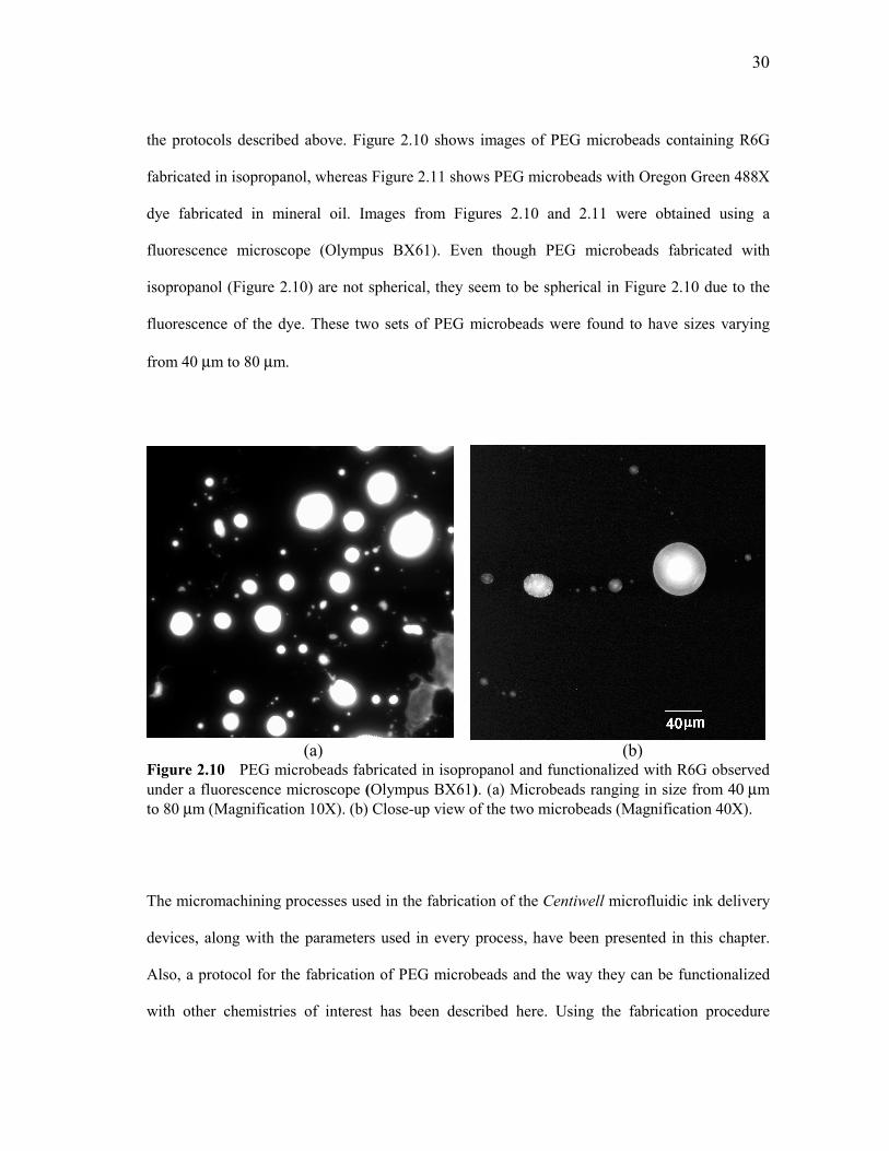
30
the protocols described above. Figure 2.10 shows images of PEG microbeads containing R6G
fabricated in isopropanol, whereas Figure 2.11 shows PEG microbeads with Oregon Green 488X
dye fabricated in mineral oil. Images from Figures 2.10 and 2.11 were obtained using a
fluorescence microscope (Olympus BX61). Even though PEG microbeads fabricated with
isopropanol (Figure 2.10) are not spherical, they seem to be spherical in Figure 2.10 due to the
fluorescence of the dye. These two sets of PEG microbeads were found to have sizes varying
from 40 µm to 80 µm.
(a) (b)
Figure 2.10 PEG microbeads fabricated in isopropanol and functionalized with R6G observed
under a fluorescence microscope (Olympus BX61). (a) Microbeads ranging in size from 40 µm
to 80 µm (Magnification 10X). (b) Close-up view of the two microbeads (Magnification 40X).
The micromachining processes used in the fabrication of the Centiwell microfluidic ink delivery
devices, along with the parameters used in every process, have been presented in this chapter.
Also, a protocol for the fabrication of PEG microbeads and the way they can be functionalized
with other chemistries of interest has been described here. Using the fabrication procedure

31
described in this chapter, a Centiwell substrate with a 96-microwell array, with depth of
microwells of 5.8 µm, was obtained. Also, PEG microbeads of sizes ranging from 40 µm to 80
µm were fabricated. The next chapter of this thesis describes the integration of the microwell
array to the Peltier coolers and the incorporation of the PEG microbeads into the microwells, as
well as the experimental apparatus for the delivery of ink to the pens used for the DPN process.

32
Figure 2.11 PEG microbeads fabricated in pure mineral oil and functionalized with Oregon
Green 488X (Magnification 10X).

33
CHAPTER III
EXPERIMENTAL APPARATUS AND TESTING OF THE CENTIWELL
MICROFLUIDIC INK DELIVERY DEVICE
The Centiwell microfluidic device consists of a microwell array fabricated on a silicon substrate.
The silicon substrate is mounted on a thermoelectric module to lower the temperature of the
substrate. This is used to condense water droplets in the microwells. PEG microbeads dispensed
into the microwells have a dual function. First, their hygroscopic property is used to capture the
condensed water droplets preventing their evaporation from the microwells. Second, PEG
dissolves in the condensed water forming the solution that serves as an ‘ink’ for the DPN
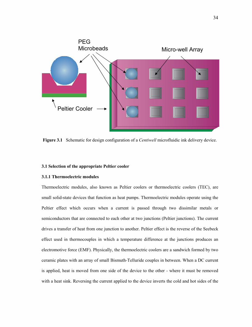
process. The schematic for the design configuration of the Centiwell microfluidic device is
shown in Figure 3.1. The complete design of Centiwell comprises the microwell array on a
silicon substrate, the thermoelectric module integrated to the back side of the silicon substrate,
and the positioning of PEG microbeads into the microwells. This figure shows only part of the
complete microwell array for better conceptualization. The fabrication of the microwell array on
a silicon substrate and the fabrication of PEG microbeads have been described in the previous
chapter. Three topics are discussed in the present chapter: 1) thermal calculations to select a
suitable thermoelectric module, 2) preliminary tests of the components of the Centiwell device,
3) experimental apparatus.
34
Figure 3.1 Schematic for design configuration of a Centiwell microfluidic ink delivery device.
3.1 Selection of the appropriate Peltier cooler
3.1.1 Thermoelectric modules
Thermoelectric modules, also known as Peltier coolers or thermoelectric coolers (TEC), are
small solid-state devices that function as heat pumps. Thermoelectric modules operate using the
Peltier effect which occurs when a current is passed through two dissimilar metals or
semiconductors that are connected to each other at two junctions (Peltier junctions). The current
drives a transfer of heat from one junction to another. Peltier effect is the reverse of the Seebeck
effect used in thermocouples in which a temperature difference at the junctions produces an
electromotive force (EMF). Physically, the thermoelectric coolers are a sandwich formed by two
ceramic plates with an array of small Bismuth-Telluride couples in between. When a DC current
is applied, heat is moved from one side of the device to the other - where it must be removed
with a heat sink. Reversing the current applied to the device inverts the cold and hot sides of the
PEG Microbeads Micro-well Array
Peltier Cooler

35
module. Figure 3.2 shows a sketch of a thermoelectric module attached to a heat sink and to the
object to be cooled. Unfortunately, thermoelectric modules are not very efficient and can draw
several amperes of current (and therefore a high amount of power). However, one of the greatest
advantages of these devices is that they can allow cooling below ambient temperature and can be
very compact and inexpensive.
Figure 3.2 Sketch showing a Peltier cooler mounted on a heat sink to dissipate the heat pumped
from the object on the top.
3.1.2 Thermal calculations
Currently, there is a wide variety of commercial thermoelectric modules of different sizes and
cooling power that are designed for different applications. Therefore, it was necessary to choose
the device that best fits the needs of this particular application. The thermoelectric modules used
in the present work were needed to cool the substrate at the location of the microwell array to a
temperature below the dew point, so that water can be condensed in the microwell array from the
ambient humidity. In order to choose a commercial thermoelectric module that could fit the
needs of the Centiwell device, some calculation were performed as described below.

36
3.1.2.1 Dew point temperature
The temperature at which a mixture of unsaturated moist air becomes saturated is known as dew
point.78 Figure 3.3 shows T-s thermodynamic diagram of the process. State 1 refers to the
superheated mixture, whereas State 2 is the dew point temperature for the mixture at State 1. If
any of the steam condenses, then saturated water appears at State 3. Since the mixture goes from
an unsaturated state with relative humidity less than one to saturated state with relative humidity
equal to unity, the calculation of the dew point temperature depends directly on the relative
humidity of the system. The relative humidity, or humidity ratio, can be expressed as:
g
v
p
pRH = (3.1)
where, pg is the corresponding saturated pressure of the saturated mixture at temperature T1 and
pv is the partial pressure at State 1. For a given temperature and humidity ratio of a moist air
mixture, the pressure pg for the saturated state at the given temperature can be found from steam
thermodynamic data. Using Equation 3.1 the vapor pressure at State 1 can be calculated. Finally,
the corresponding saturation temperature (dew point temperature) for pv is obtained using steam
thermodynamic data. Table 3.1 shows the dew point temperature calculated at 25 oC for various
humidity ratios. The humidity ratios considered in Table 3.1 are in accordance to the conditions
at which the Centiwell device was tested.
Table 3.1 Dew point temperature for different relative humidities at an ambient temperature of
25 oC.
Relative humidity (%) Dew point temperature (oC)
25 3.25
30 6.1
35 8.3
40 10.2
45 12.1

37
Figure 3.3 Thermodynamic chart representing the procedure for obtaining the dew point of a
moist air mixture at State 1.
3.1.2.2 Heat conduction through the substrate
As mentioned above, the purpose of the integration of a thermoelectric module in the Centiwell
device is to obtain water condensation in the microwell array. Thus, the thermoelectric module
must be capable of removing heat at a rate required to reach the dew point temperature at the
surface of the microwells. Heat transfer calculations were performed to estimate the operating
temperature of the Peltier cooler and for obtaining the dew point temperature at the top of the
substrate where the microwell array is located. Experiments for testing the Centiwell device for
condensation of water were performed at humidity ratios ranging from 0.3 to 0.4 and at an
ambient temperature of 25 oC. Therefore the heat transfer calculations were performed for a
relative humidity of 25% as a representative value. In the thermal analysis, the only heat source
for the silicon substrate was considered to be from natural convection of air on the top of the
microwell array. A heat transfer coefficient of 10 W/m2K was assumed.
79 The contact resistance
between the thermoelectric cooler and the back side of the substrate was neglected. To satisfy
this condition, thermal grease (340 Silicone Heat Sink Compound, from Dow Corning

38
Corporation) was used at the interface of the cooler and the substrate. The thermal conductivity
of silicon has been taken as 148 W/mK.80 Newton’s law of cooling was used (Eq. 3.2) for the
calculation. For an ambient temperature of 25 oC and a relative humidity of 25%, the heat flux at
the top surface of the silicon substrate was obtained as 217.5 W/m2K.
( )∞−= TThq Dew" (3.2)
In order to maintain the top surface of the silicon substrate at the dew point temperature, all the
heat gained by the substrate by convection must be dissipated or removed by the thermoelectric
cooler. Applying Fourier’s law in one dimension (see Equation 3.3) and considering the distance
between the bottom of the substrate and the bottom of the microwell as 490 microns, the
temperature at the bottom of the substrate is obtained as 3.25 oC. The temperature difference
between the top and bottom surface of the silicon substrate is practically negligible due to the
small value of the thickness of the substrate. Therefore, the maximum cold side temperature of
the thermoelectric module was determined to be 3.25 oC (as mention above, the contact
resistance was neglected).
dy
dTkq −=" (3.3)
Finally, the maximum power of the thermoelectric cooler was determined by performing a
transient heat transfer analysis for the system. Typically, the maximum heat flux occurs at the
beginning of the transient process since at this point the temperature difference is maximum. The
transient analysis was performed by numerically solving Equation (3.4), where α is the thermal
diffusivity (for silicon α = 90.7 x 10⁻⁶ m
2/s).
80 Finite differences method was used to obtain the

39
solution and the calculations were performed using the FORTRAN program Peltier.f90 (see
Appendix A.1). Figure 3.4 shows the temperature profiles through the thickness of the silicon
substrate for different times. The time needed to reach the steady state was calculated to be 0.01
seconds. The heat load with respect to time for different humidity conditions is shown in Figure
3.5. It can be seen from this figure that the maximum heat load occurs at the beginning of the
process and it is higher for lower humidity ratios. The heat load shown in Figure 3.5 was
calculated by multiplying the heat flux by the area of the microwell array. The area of the
microwell array is calculated by multiplying the square of the pitch between the microwells
times the number of microwells. This area was calculated as 6.1 x 10⁻⁹ m
2.
2
21
y
T
t
T
∂
∂=
∂
∂
α (3.4)
Based on the thermal calculation described above, the thermoelectric module TE-31-0.6-0.8
(manufactured by TE Technology, Inc) was chosen as a suitable Peltier cooler for the Centiwell
microfluidic device. The characteristics of this particular thermoelectric module are listed on
Table 3.2 and the dimensions of the cooler are shown in the schematic in Figure 3.6. The size of
the Peltier cooler is 0.8 cm by 0.8 cm. It can be observed from plot in Figure 3.5 that the
maximum heat load to cool down the silicon substrate for a relative humidity of 25% is 4.036 W.
The thermoelectric module TE-31-0.6-0.8 meets these dissipation requirements since it is rated
for a maximum cooling load of 4.8 W.

40
275
280
285
290
295
300
0 50 100 150 200 250 300 350 400 450 500
Substrate Thickness (µµµµm)
Tem
pera
ture
(K
)
TIME=0
TIME=0.00009000
TIME= 0.00040499
TIME= 0.00101570
TIME= 0.00217283
TIME= 0.01040773t
Figure 3.4 Result from calculations for temperature profiles across the thickness of the
Centiwell substrate at different times.

41
0
0.5
1
1.5
2
2.5
3
3.5
4
4.5
0 0.002 0.004 0.006 0.008 0.01 0.012
Time (s)
Heat (W
)HR=25%
HR=30%
HR=35%
HR=40%
HR=45%
Figure 3.5 Calculated values for heat load variation with respect to time for different humidity
ratios.
Figure 3.6 Sketch showing the shape of the TE-31-0.6-0.8 thermoelectric module.

42
Table 3.2 Operation rating of the thermoelectric module TE-31-0.6-0.8 (Manufacturer: TE
Technology, Inc.).
I_max (amps) 2.1
Q_max (watts) 4.8
V_max (volts) 3.8
DT max (T_hot = 300 K) 67
A (mm) 8
B (mm) 8
C (mm) 8
D (mm) 8
H (mm) 2.55
3.2 Testing of the Centiwell microfluidic device
Before assembling all component parts of the Centiwell device, preliminary tests were performed
to check the proper operation of the Peltier cooler and to assure the expected water condensation
on the microwell array. Experiments for testing the Centiwell microfluidic device were
conducted at the Center for Integrated Micromechanical Systems of Texas A&M University.
3.2.1 Condensation experiments in Centiwell substrate without PEG microbeads
Preliminary experiments were conducted to test the performance of the Peltier cooler on the
Centiwell device. The cold side of the Peltier cooler was attached to the back side of the silicon
substrate using thermal grease (340 Silicone Heat Sink Compound, from Dow Corning
Corporation) to reduce the thermal contact resistance between the two surfaces. The heat
removed by the cooler from the silicon substrate is rejected on the hot side of the cooler onto a
heat sink (411625B02500 by ThermaFlo). The preliminary experiments were performed at a
relative humidity of 35% at which the dew point temperature was calculated to be 8.3 oC (from
Table 3.1). The operation current for the Peltier cooler ranged from 0.08 to 0.280 amperes (with

43
corresponding voltage values ranging from 0.250 V to 0.750 V). This resulted in cooling of the
top surface of the silicon substrate and the operating temperatures ranged between 18 oC and 2
oC, respectively.
Drop-wise condensation was found to occur on the surface of the microwell array at
temperatures below the dew point. Figure 3.7 shows a sequence of 6 images taken at different
stages of the experiment. Figure 3.7a shows the microwell array at the initial condition before
the Peltier cooler was in operation. Then, the power was connected to the Peltier cooler and a
voltage of 0.750 V was applied with a current of 0.28 A. The temperature of the substrate
decreased to about 2 oC and very small water droplets less than 1 micron in diameter condensed
instantaneously on the surface of the substrate (Figure 3.7b). At later times, the size of the
droplets grew forming a uniform distribution of droplets on the substrate. At this stage, droplets
started to form at the corners of the microwells without occupying the whole cavity of the
microwell (Figure 3.7c). After about 4 min of cooling (Figure 3.7d), droplets grew in size and
covered almost the entire surface of the substrate. At this point, droplets inside the microwell
merged together forming a single droplet that occupied almost the complete volume of the cavity
but they still maintained a fairly rounded shape. Droplets outside the microwells were found to
be a little smaller in size (about 30 microns) than the ones that formed inside the microwells.
Power to the Peltier cooler was disconnected at this stage and the water droplets evaporated
quickly. Figure 3.7e shows a picture of the substrate 14 seconds after the power was
disconnected. It can be seen from this picture that only a few droplets outside the microwell
array remained and only a few microwells contained tiny droplets. Finally, after about 25
seconds of power disconnection the condensed water had evaporated completely all over the
substrate (Figure 3.7f).

44
(a) (b)
(c)
Figure 3.7 Sequence of images for several stages of condensation process on the Centiwell
without PEG microbeads. (a) Initial condition of the microwell array, (b) condensation begins
immediately after reaching the dew point temperature, (c) growth of water droplets, where
droplets at the corners of the microwells are observed, d) droplets occupying the entire volume
of the microwells, e) power disconnected to the Peltier cooler causes condensed water to
evaporate, f) 25 seconds after disconnecting the cooler, all of the condensed water was observed
to evaporate instantaneously from a major part of the substrate.

45
(d)
(e) (f)
Figure 3.7 Continued.

46
3.2.2 Positioning of PEG microbeads
The volume of the condensed droplets obtained using the procedure described in the previous
section is miniscule and the droplets are lost by evaporation almost instantaneously after the
power is disconnected to the Peltier cooler. However, it is desired to keep the water condensed
inside the microwell for longer periods of time, so that the dipping procedure for DPN can be
carried out. To address this issue, a hygroscopic material was incorporated to prevent the sudden
evaporation of water from the microwells. Polyethylene glycol (PEG) microbeads (fabricated
according to the protocols described in Chapter II) were placed in every microwell. Using PEG
conferred several advantages: 1) it is a hygroscopic material that traps the condensed water
inside the microwells, 2) it is water soluble, so that it can form a small solution that can be used
to coat the “pen” in DPN process, 3) it can be functionalized with different bio-chemistries, so
that solutions can form inside the microwells containing a desired chemistry which can then be
used for DPN.
(a) (b)
Figure 3.8 Positioning of PEG microbeads into microwells using a micromanipulator. (a) PEG
microbead placed near the top-left-corner microwell, (b) PEG microbead moved with the
micromanipulator to place it in the microwell.

47
Unfunctionalized PEG microbeads were manually placed into the microwells using a
micromanipulator (Figure 3.8). In a commercial application the placement of microbeads can be
automated using pneumatic robotic handlers (e.g. SPBIOII Spotter by Mirai Bio, Hitachi
Software).
Another method for placement of microbeads was achieved by depositing a number of PEG
microbeads over the array of microwells. Using the edge of a filter paper the microbeads were
swept along the two directions of the microwell array, back and forth, several times to
manipulate the microbeads into the microwells. Subsequently a final sweep was performed to
remove excess PEG particles from the surface of the Centiwell substrate. With this technique the
microbeads of smaller size were trapped into the microwells, and the excess microbeads were
removed from the surface. Figure 3.9 shows the microwell array with PEG microbeads deposited
in each microwell. In the figure a brighter spot at the center of every microwell can be observed
which corresponds to top of the spherical PEG microbeads.
Figure 3.9 Microwell array with PEG microbeads (fabricated using mineral oil) placed in the
microwells.
PEG
microbead
Microwell
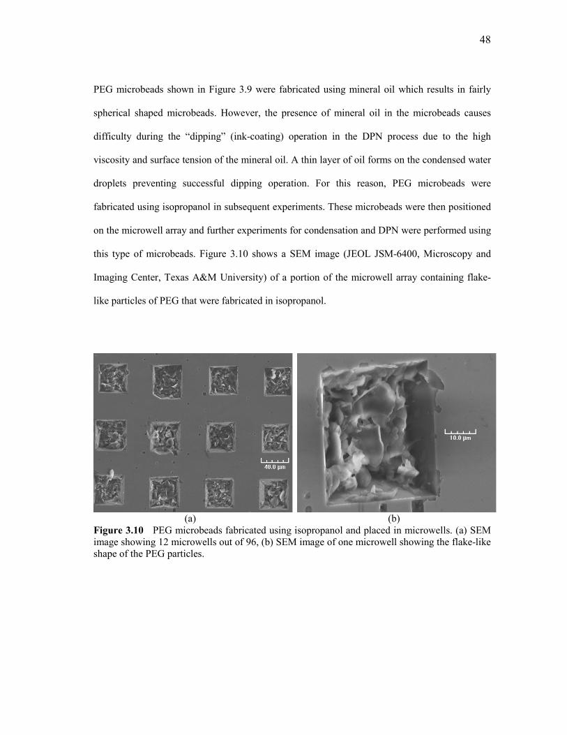
48
PEG microbeads shown in Figure 3.9 were fabricated using mineral oil which results in fairly
spherical shaped microbeads. However, the presence of mineral oil in the microbeads causes
difficulty during the “dipping” (ink-coating) operation in the DPN process due to the high
viscosity and surface tension of the mineral oil. A thin layer of oil forms on the condensed water
droplets preventing successful dipping operation. For this reason, PEG microbeads were
fabricated using isopropanol in subsequent experiments. These microbeads were then positioned
on the microwell array and further experiments for condensation and DPN were performed using
this type of microbeads. Figure 3.10 shows a SEM image (JEOL JSM-6400, Microscopy and
Imaging Center, Texas A&M University) of a portion of the microwell array containing flake-
like particles of PEG that were fabricated in isopropanol.
(a) (b)
Figure 3.10 PEG microbeads fabricated using isopropanol and placed in microwells. (a) SEM
image showing 12 microwells out of 96, (b) SEM image of one microwell showing the flake-like
shape of the PEG particles.

49
Another trial for placing microbeads in the microwells was done using polystyrene
microspheres. Figure 3.11 shows a SEM picture of the empty microwells and microwells
containing Polystyrene microspheres of 25 microns diameter (manufactured by Polysciences,
Inc). It can be seen from Figure 3.9, 3.10, and 3.11 that the microbeads are placed inside the
microwells only and the rest of the substrate is clean. This procedure is especially important to
avoid cross contamination when using different chemical species in different microwells.
(a) (b)
Figure 3.11 SEM image showing a section of the array. (a) Empty microwells, (b) Polystyrene
microbeads placed in the microwells.
3.2.3 Condensation experiments incorporating PEG microbeads
After placing the PEG microbeads (fabricated using isopropanol) in the microwells, another
condensation experiment was performed to test the behavior of the condensed water with the
hygroscopic material. A voltage was applied to the Peltier cooler in order to lower the
temperature of the silicon substrate. The ambient humidity ratio during these experiments was
recorded to be 30% and the corresponding dew point was calculated to be 6.2 oC. Therefore a
voltage of 0.7 V with a corresponding electrical current of 0.28 A was applied to get the surface
temperature cooled to 2 oC. Once the temperature of the silicon substrate reached below the dew

50
point, condensed droplets of water were observed to form instantaneously on the surface (Figure
3.12). The size of the droplets was observed to be approximately 5 microns. At this time the
power to the Peltier cooler was disconnected. It was observed that the condensed water droplets
on the surface of the substrate evaporated immediately after the power to the Peltier cooler was
disconnected. However the water droplets trapped in the microwells were observed to dissolve
the PEG microbeads and remain in the microwells when the power to the Peltier cooler was
disconnected (Figure 3.13). Since PEG is hygroscopic it spontaneously adsorbs water from the
ambient humidity. Due to this property the PEG resists water molecules in the solution from
evaporating.
Figure 3.12 Image from microscope showing
condensed water droplets.
Figure 3.13 Image showing PEG solutions in
water trapped in the microwells while the
condensed water droplets on the surface have
evaporated after disconnecting power to the
Peltier coolers.
3.3 Experimental apparatus
Once all preliminary tests described in previous sections were finished, all parts of the Centiwell
device were assembled together in order to conduct the DPN experiments to prove the

51
functionality of the device. The experimental apparatus is shown schematically in Figure 3.14.
The device was mounted on the stage of the Atomic Force Microscope (AFM, Nanoscope IIIa
from Digital Instruments). The heat sink used in the preliminary experiments for testing the
Peltier cooler was not used in these experiments since the AFM stage served as a substitute. The
hot side of the module was placed in contact with the metallic stage of the AFM which was
found to be sufficient to handle the heat from the Peltier device. To improve the energy
dissipation from the Peltier cooler to the AFM stage, thermal grease was applied at the interface
of both surfaces. Figure 3.14a, shows the Centiwell device mounted on the AFM stage at the
initial condition. At this point, PEG microbeads were present in the microwells and the AFM tip
was positioned just above the microwells. The power was then connected to the Peltier cooler
and drop-wise condensation occurred on the surface of the Centiwell substrate. After about 5
minutes, the power was disconnected and the condensed water evaporated from the substrate
except for the water condensed in the microwells which was trapped by the PEG microbeads.
Once the PEG solution was obtained in the microwells, the AFM tip was lowered and dipped
into the microwells containing the PEG solution (Figure 14b). This process is known as
“dipping”, “coating” or “inking” of the “pen” (scanning probe) for DPN writing. The dipping of
the AFM tip lasted about 2 minutes after which the tip was raised by moving the stage vertically
downwards and the Centiwell device was dismounted from the stage of the AFM. The tips used
in the experiments are non-conductive silicon nitride based scanning probes (model NP-20, with
a Top-60-nm-Au/ Bot-15-nm-Cr coating on the back side, manufacturer: Veeco Products).
When the inking process was concluded and the Centiwell device was dismounted, a mica
substrate (PELCO® Mica Sheets, Grade V5, from Ted Pella, Inc) was placed on the AFM stage
and the DPN writing was carried out. The process was repeated several times to generate

52
different patterns. The motion of the AFM tip to perform the DPN writing was controlled using
the programs Lines.txt, TAMU.txt. The source code of such programs can be seen in Appendix
A.2.
AFM STAGE
Peltier Cooler
Centiwell Substrate
AFM STAGE
Peltier Cooler
Centiwell Substrate
(a) (b)
Figure 3.14 Schematic for “dipping” experiments conducted by mounting the Centiwell
microfluidic device on an AFM stage. (a) Initial state of the device before operation, (b) dipping
of the AFM tip in a microwell after condensation process.
A description of the preliminary experiments of the Centiwell microfluidic device was reported
in the present chapter. These experiments include the condensation of water on the microwell
array before and after the positioning of PEG microbeads into the microwells. Thermal
calculations to choose the appropriate thermoelectric cooler for Centiwell were also presented.
Finally, a procedure for dipping experiments was described. Results of DPN experiments,
including the ink-coating experiments and actual DPN patterning, are described in next chapter.
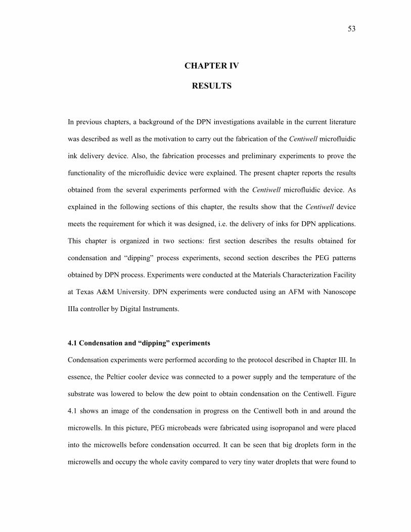
53
CHAPTER IV
RESULTS
In previous chapters, a background of the DPN investigations available in the current literature
was described as well as the motivation to carry out the fabrication of the Centiwell microfluidic
ink delivery device. Also, the fabrication processes and preliminary experiments to prove the
functionality of the microfluidic device were explained. The present chapter reports the results
obtained from the several experiments performed with the Centiwell microfluidic device. As
explained in the following sections of this chapter, the results show that the Centiwell device
meets the requirement for which it was designed, i.e. the delivery of inks for DPN applications.
This chapter is organized in two sections: first section describes the results obtained for
condensation and “dipping” process experiments, second section describes the PEG patterns
obtained by DPN process. Experiments were conducted at the Materials Characterization Facility
at Texas A&M University. DPN experiments were conducted using an AFM with Nanoscope
IIIa controller by Digital Instruments.
4.1 Condensation and “dipping” experiments
Condensation experiments were performed according to the protocol described in Chapter III. In
essence, the Peltier cooler device was connected to a power supply and the temperature of the
substrate was lowered to below the dew point to obtain condensation on the Centiwell. Figure
4.1 shows an image of the condensation in progress on the Centiwell both in and around the
microwells. In this picture, PEG microbeads were fabricated using isopropanol and were placed
into the microwells before condensation occurred. It can be seen that big droplets form in the
microwells and occupy the whole cavity compared to very tiny water droplets that were found to

54
form around the microwells. It was observed that as soon as the droplets near the microwells
started to form, they merged into the microwells filling the cavities. The droplets formed around
the microwells were found to evaporate as soon as the power to the Peltier cooler was
disconnected.
Figure 4.1 Condensation on Centiwell substrate. Image shows water droplets merging into the
cavities at the location of the microwell array.
A SEM picture of the microwells with PEG microbeads was taken before and after the
condensation experiments for comparison. Two SEM pictures presented in Figure 4.2 show the
difference of the PEG material due to the condensation process. Before water condensation,

55
flake-like PEG microbeads were present in the microwells (Figure 4.2a). A PEG solution was
then formed when water condensation occurred. It can be observed in Figure 4.2b that PEG
material looks like a densified amorphous mass in the microwells after the condensation. SEM
picture shown in Figure 4.2b was taken several days after performing the condensation
experiments, allowing enough time for the condensed water to dry out even in the presence of
PEG. The purpose of these two images in Figure 4.2 is to emphasize the fact that a solution was
formed inside the microwells and this is proved with the change in shape of the PEG material
inside the microwells.
Another experiment was performed for the ‘inking’ of the AFM tip. In this experiment, the
Centiwell substrate was mounted on the stage of the AFM. Power to the Peltier cooler was
connected and condensation occurred as described before. Once the PEG solution was formed
due to the water condensation process, the next step in the experiments was to ‘dip’ the ‘pen’ and
coat it with the PEG solution for successive writing by DPN. In this case, the ‘pen’ used for the
experiments was the tip of a silicon nitride AFM probe (model NP-20, with a Top-60-nm-Au/
Bot-15-nm-Cr coating on the back side, manufacturer: Veeco Products) used for contact mode
AFM. The experimental apparatus for coating the AFM tip was described in Chapter III. The
AFM tip was loaded in the tip holder.

56
(a) (b)
Figure 4.2 PEG microbeads fabricated in isopropanol and placed inside microwells. (a) PEG
microbeads before water condensation occurred. (b) PEG densified amorphous mass in every
microwell after condensed water dissolved the microbeads.
Once water condensation was obtained on the Centiwell substrate, the power was disconnected
to allow water evaporation outside of the microwell. The AFM tip was then lowered by moving
the AFM stage upwards. The pen was “dipped” into the microwells for 2 minutes. During the
‘inking’ process, PEG particles from the solution in the microwells are presumed to be
transported to AFM tip and to coat the surface of the tip. The dipping time used in the present
experiment was found to be optimal for obtaining a well coated tip. Figure 4.3 shows the state of
the tip during dipping operation. Figure 4.3a shows the AFM tip before dipping and positioned
just above the microwells containing the PEG solution. In Figure 4.3b the tip was dipped into the
microwells. Comparison of the two images in Figure 4.3 shows the different contrast of the light
reflected from the back of the scanning probe tip when it is dipped in the microwells (Figure
4.3b) compared to just prior to dipping (Figure 4.3a). This is caused by the different angle of the
cantilever when it is pulled into the microwells by capillary forces. This occurs when the tip
contacts the liquid meniscus during approach of the tip into the microwells.

57
After the dipping process, a SEM picture of the Centiwell substrate was obtained at the same
location where the scanning probe tip was dipped. It can be observed in Figure 4.4 that PEG
material was not distributed uniformly in the microwell at the time this SEM image was
obtained. Instead, some PEG material was missing in the right-hand side of the microwell at
exactly the same location where the AFM tip was positioned during the dipping process. The
AFM tip has a finite capability for loading of the PEG based ink. Hence, this suggests that the
large amount of PEG material that was removed from inside the microwell was transferred
probably to the AFM tip as well as to the cantilever during the dipping process.
(a) (b)
Figure 4.3 Dipping process of the AFM tip. (a) AFM tip close to the microwell before dipping,
(b) AFM tip dipped in the microwell.
4.2 DPN patterns
The last step in the DPN process is the lithography operation of the chemistry coated on the
scanning probe onto an appropriate substrate. As mentioned in Chapter I, the ambient humidity
plays an important role in the transport of the ‘ink’ to the substrate during the lithography
process. In this work, several DPN experiments were carried out at different humidity ratios and

58
different velocities of the AFM tip for the patterning of PEG. The results obtained from these
experiments are described below.
Figure 4.4 Appearance of the PEG material inside the microwell at which the dipping
operation was performed.
Several intermediate steps are involved in the DPN process, some of which were described in the
previous chapters. First, the Centiwell device was mounted on the AFM stage and condensation
on the microwell array was obtained by connecting the power to the Peltier cooler. Second, the
AFM tip was lowered and dipped into a microwell for coating with PEG solution. Third, the
AFM tip was retracted from the microwells and the Centiwell device was dismounted from the
AFM stage. Finally, a mica substrate (PELCO® Mica Sheets, Grade V5, from Ted Pella, Inc)

59
was placed immediately on the AFM stage and the DPN writing was carried out. A set of three
lines of PEG were patterned by the DPN process using an AFM tip coated with PEG. The
patterned lines were then imaged by lateral force microscopy (LFM) and are shown in Figure
4.5. The program LINES.txt was used to control the motion of the AFM tip for the DPN
patterning (see Appendix A.2).
Figure 4.5 Lateral force microscopy image of a set of three lines patterned with PEG by DPN.
Ambient humidity was recorded to be 60%.

60
After DPN patterning, the lines were scanned with the same PEG-coated tip at a scan rate of 6.7
Hz (tip velocity: 407 µm/s). The lines shown in Figure 4.5 are 5 µm in length and were patterned
at three different writing speeds of 5 µm/s, 2 µm/s, and 1 µm/s. The ambient relative humidity
was registered to be of 60% at the time of the DPN experiment. The thickness of the lines varied
with the writing speed. The first line (from left to right), corresponding to a writing speed of 5
µm/s, was measured to be 285-nm wide; the second line (writing speed 2 µm/s) was 410 nm; and
the third line (writing speed 1 µm/s) was 450 nm. A PEG spot can be observed near the line on
the extreme right. This spot was formed at the end of the patterning (lithography) operation when
the tip stayed in contact with the mica substrate for about 45 seconds prior to disengaging the tip
(pen). The spot was measured to be 800 nm in diameter. Traces of PEG materials were also
observed along the trajectory of the tip while moving from one line to the next. The
displacement of the tip from one line to the next was performed with the tip in contact with the
mica substrate but at a relatively high speed (20 µm/s). The Section analyses that were
performed for measuring the width of the patterned lines are shown in Appendix B.
Another set of three lines of PEG was patterned by DPN process at relative ambient humidity of
29% (Figure 4.6). The coating of the scanning probe was performed similarly to the process
described earlier in this chapter. It was found that at this low value of ambient humidity
discontinuous lines of PEG were formed by the DPN process probably because a stable meniscus
was not sustained between the tip and the substrate. The lines could be observed by LFM using
the same PEG-coated tip at a scan rate of 6.1 Hz (tip velocity: 366 µm/s). The lines were
patterned at three different speeds of 2 µm/s, 1 µm/s, and 0.5 µm/s and the corresponding
thicknesses of the lines were found to be 130 nm, 235 nm, and 285 nm, respectively. A PEG spot
was also found for this experiment which formed at the initial stage of the DPN process during

61
approach of the tip on the substrate. The exact contact time for the formation of this spot was not
recorded but was presumably less than 1 minute. The thickness of the spot was 400 nm.
Figure 4.6 Discontinuous lines of PEG formed during patterning at a high speed using the DPN
process. The experiments were performed at an ambient humidity of 29%.

62
DPN patterning of a third set of three lines was performed for tip speeds of 2 µm/s, 1 µm/s, and
0.5 µm/s at an ambient humidity of 65%. Figure 4.7 shows the LFM image of the set of three
lines obtained with the PEG-coated tip at a scan rate of 6.7 Hz (tip velocity: 407 µm/s). For this
case, the line pattern at a writing speed of 2 µm/s is quite thin that it is difficult to distinguish in
the image (left-hand side of the picture in Figure 4.7). Although this line could not be measured
properly, the section analysis of the image suggested that this line is less than 150 nm in width.
Measurements for the other two lines reveals line widths of 600 nm for the middle line (writing
speed of 1 µm/s) and 1.12 µm for the line on the extreme right (writing speed of 0.5 µm/s).
It was found from the experiments that nano-patterning of PEG was strongly affected by the
ambient humidity, producing larger width of the lines at higher humidity ratios. The tip speed
(“writing speed”) was also found to affect the line width. In general, it was found that slower
translation speeds of the AFM tip produced thicker lines. However, it was also observed that a
PEG pattern was difficult to obtain when the writing speeds were less than 0.5 µm/s.
A plot showing variation of line width for nano-patterned features of PEG versus writing speed
is presented in Figure 4.8 for different humidity ratios. The three curves from Figure 4.8 show
that for the nano-patterned lines the width of the lines decreases as the tip speed increases. The
single data point for the highest humidity and highest tip speed has a larger variation in width
than the other points. This data point shows that line widths are nearly equal for humidity ratios
of 29% and 65% for the same tip speed (2 µm/s). This trend does not agree with the humidity
trends observed for the other data points plotted in Figure 4.8. It is worth pointing out that the
experimental setup did not have any humidity control instrumentation. Probably the ambient
humidity in the vicinity of the tip decreased during the course of this particular experiment

63
causing the observed variability in the line width. Access to good humidity control apparatus
could have prevented such variability in the data.
Figure 4.7 LFM images showing a set of three PEG lines patterned by DPN at an ambient
humidity of 65%.

64
0
200
400
600
800
1000
1200
0 1 2 3 4 5 6
Tip speed (µµµµm/s)
Lin
e w
idth
(nm
)HR=65%
HR=60%
HR=29%
Figure 4.8 Variation of line width for nano-patterned features of PEG versus writing speed
DPN is a flexible technology that allows not only the patterning of straight lines or dots but also
the fabrication of more complex structures at the nanoscale level. Patterning of complex
structures at the nanoscale level is especially important for applications in fields such as
microelectronics or biochemistry, where the manipulation and placement of materials in specific
positions is desirable. To show proof of concept, a more complex PEG pattern was fabricated
using DPN process. The letters “TAMU” were patterned by DPN (as the acronym for Texas
A&M University). As before, the delivery of the PEG ink to the scanning probe was carried out
by means of the Centiwell microfluidic device. The letters were patterned twice without re-
inking the AFM tip and similar results were found. The motion of the tip to fabricate the pattern
was controlled by the AFM controller using the computer code TAMU.txt (see Appendix A.2).

65
Figure 4.9 LFM image of the TAMU logo patterned with PEG by DPN.
Figure 4.9 shows a LFM image of the first set of “TAMU” pattern obtained by DPN using PEG.
The writing speed was set at 0.5 µm/s and the ambient humidity was recorded as 65%. The LFM
image was obtained at a scan rate of 6.8 Hz (tip speed: 407 µm/s). Measurements of the lines
forming the letters showed thicknesses ranging from 350 nm – 800 nm. Since the AFM used for
the DPN experiments does not have capability for close-loop control, there is considerable mis-
alignment of the letters during the nano-patterning operation.

66
Figure 4.10 LFM image of the second TAMU logo patterned with the same PEG-coated tip
that generated the pattern in Figure 4.9.
The second set of “TAMU” pattern is shown in Figure 4.10 which was obtained by LFM at a
scan rate of 6.8 Hz (tip speed: 407 µm/s). This pattern was nano-fabricated with the same PEG-
coated tip used for the lithography of the first set of “TAMU” pattern. The writing speed was the
same as in the previous pattern (0.5 µm/s) and as well as the ambient humidity (65%). The only

67
appreciable difference between the two patterns was that the lines forming the letters were
slightly thinner in the second pattern, ranging from (300 nm – 600 nm)
Finally, an interesting phenomenon was observed for large contact times and is reported here.
After long contact times (~ 2 hours) of the tip coated with PEG and in contact with the mica
substrate fractal patterns were obtained from LFM scans of the mica surface. This is believed to
occur by ‘anomalous’ diffusion of PEG molecules on the substrate. Similar results have been
reported for DPN operations of DDA performed on mica for long contact times.53 However,
DPN patterns were observed only by LFM and the fractal form was of the order of 1 µm – 2 µm
in size. In the present work, several fractal patterns were observed even in the height information
of contact mode AFM with lengths of the order of 30 µm – 60 µm. The areas containing the
fractal patterns were scanned several times and even after repeated scans the shape of the
patterns were not altered. This suggests that the fractal patterns of PEG formed a stable structure
despite the weak binding affinity of PEG molecules to the mica surface. Figure 4.11 shows
several fractal patterns obtained by DPN for large contact times.

68
(a) (b)
(c) (d) Figure 4.11 Height information of contact AFM showing fractal shapes formed during DPN of
PEG molecules on a mica substrate. The contact time of the scanning probe tip on the mica
surface was approximately 2 hours.

69
CHAPTER V
CONCLUSIONS
The Centiwell microfluidic ink delivery device was designed, fabricated, assembled, and tested
successfully in this study. This work shows that the Centiwell microfluidic device can be used as
an ink delivery system for maximizing the throughput of DPN (and other SPL techniques) to 96
different “inks” (or to 96 unique chemical species). The microwells in the Centiwell were
designed to achieve volumes of less than 1 pico-liter each. This can enable significant cost
savings for nanolithography of expensive biological samples and reagents.
Polyethylene-glycol (PEG) microbeads were fabricated and used to test the functionality of the
Centiwell microfluidic device. PEG microbeads used in the present work have a dual function.
First, their hygroscopic property is used to capture the condensed water droplets and minimize
their evaporation from the microwells. Second, PEG dissolves in the condensed water forming
the solution that serves as an ‘ink’ for the nano-lithography process. Furthermore, it was
demonstrated that PEG microbeads can be functionalized with a desired chemistry for
subsequent use in the DPN process.
The Centiwell was successfully implemented for the intended purpose by delivering PEG
solutions (formed in the microwells by condensing water droplets from ambient humidity) to the
scanning probe tip followed by successful nanolithography of the PEG “ink”. In general, it was
found that widths of the nano-patterned lines increased as the humidity increased. The line
widths were found to decrease as the tip speed increased.

70
It was demonstrated that the proposed scheme here optimizes the DPN process for parallel-write
applications. Implementation of the proposed Centiwell microfluidic device for industrial
purposes would enhance the power of DPN for simultaneous nano-patterning of multiple inks.
This meets the current industrial standards for fluid handling in the biotechnology applications of
DPN in genomics and proteomics assays.
The Centiwell demonstrates the proof-of-concept for a microfluidic architecture that can be
expanded to handle multiple inks and to enable simultaneous nano-patterning of several
hundreds of different inks. This platform provides the capability for exponential growth in ink-
handling capacity. This approach mimics the exponential growth in device density of integrated
circuit (IC) that was responsible for the phenomenal growth of the micro-electronics industry. It
is envisioned that the utilization of a microfluidic platform such as Centiwell will serve as the
stepping stone for similar progress in technological and commercial growth of nanosystems.

71
GLOSSARY
AFM atomic force microscopy
BSA bovine serum albumin
C16S-SAM hexadecanethiolate (CH3(CH2)15S-) self-assembled monolayer
C18SH octadecanethiol (CH3(CH2)17SH)
C18S-SAM octadecanethiolate (CH3(CH2)17S-) self-assembled monolayer
DC direct current
DDA 1-dodecylamine
DI water de-ionized water
DNA deoxyribonucleic acid
DPN dip-pen nanolithography
EMF electromotive force
ESEM environmental scanning electron microscopy
HMDS Hexamethyldisilazane
IC integrated circuit
KOH potassium hydroxide
LFM lateral force microscopy
MEMS micro-electro-mechanical systems
MHA mercaptohexadecanoic acid (HS(CH2)15-COOH)
NaCl sodium chloride
ODT octadecanethiol (CH3(CH2)17SH)
PCR polymerase chain reaction
PEG polyethylene glycol

72
R6G rhodamine 6G
RH relative humidity
RIE reactive ion etching
RNA ribonucleic acid
SAM self-assembled monolayer
SEM scanning electron microscopy
SFL spray freezing into liquid
SNP single nucleotide polymorphism
SPL scanning probe lithography
SPM scanning probe microscopy
STM scanning tunneling microscopy
TEC thermoelectric cooler
UHV ultrahigh vacuum
UV ultraviolet

73
REFERENCES
1. R. P. Feynman, J. Microelectromech. Syst., 1 (1), 60 (1992).
2. N. Taniguchi, On the Basic Concept of 'Nano-Technology, Proc. Intl. Conf. Prod. Eng.
Tokyo, PartII, Japan Society of Precision Engineering, 1974.
3. Y. T Kim, A. J. Bard, Langmuir, 8, 1096 (1992).
4. M. J. Lercel, G. F. Redinbo, H. G. Craighead, C. W. Sheen, D. L. Allara, Appl. Phys. Lett.,
65, 974 (1994).
5. L. S. Xu, D. R. Allee, J. Vac. Sci. Technol., B, 13, 2837 (1995).
6. H. Sugimura, N. Nakagiri, Langmuir, 11, 3623 (1995).
7. J. K. Schoer, F. P. Zamborini, R.M. Crooks, J. Phys. Chem., 100, 11086 (1996).
8. H. U. Muller, C. David, B. Volkel, M. Grunze, J. Vac. Sci. Technol., B, 13, 2846 (1995).
9. W. Mizutani, T. Ishida, H. Tokumoto, Langmuir, 14, 7197 (1998).
10. J. Hartwich, L. Dreeskornfeld, V. Heisig, S. Rahn, O. Wehmeyer, U. Kleineberg, U.
Heinzmann, Appl. Phys. A: Mater. Sci. Process., 66, S685 (1998).
11. J. Hartwich, M. Sundermann, U. Kleineberg, U. Heinzmann, Appl. Surf. Sci., 145, 538
(1999).
12. J. M. Keel, J. Yin, Q. Guo, R. E. Palmer, J. Chem. Phys., 116, 7151 (2002).
13. G.-Y. Liu, S. Xu, Y. Qian, Acc. Chem. Res., 33, 457 (2000).
14. S. Xu, G. Liu, Langmuir, 13, 127 (1997).
15. Y. N. Xia, G. M. Whitesides, Angew. Chem., Int. Ed., 37, 551 (1998).
16. Y. N. Xia, J. A. Rogers, K. E. Paul, G. M. Whitesides, Chem. Rev., 99, 1823 (1999).
17. T. W. Odom, V. R. Thalladi, J. C. Love, G. M. Whitesides, J. Am. Chem. Soc., 124, 12112
(2002).

74
18. Y.N. Xia, G.M. Whitesides, Annu. Rev. Mater. Sci., 28,153 (1998).
19. E. Delamarche, A. Bernard, H. Schmid, B. Michel, H. Biebuyck, Science, 276, 779 (1997).
20. A. Bernard, B. Michel, E. Delamarche, Anal. Chem., 73, 8 (2001).
21. G. P. Lopez, H. A. Biebuyck, C. D. Frisbie, G. M. Whitesides, Science, 260, 647 (1993).
22. S. Gaspar, M. Mosbach, L. Wallman, T. Laurell, E. Csoregi, W. Schuhmann, Anal. Chem.,
73, 4254 (2001).
23. M. H. Hong, K. H. Kim, J. Bae, W. Jhe, Appl. Phys. Lett., 77, 2604 (2000).
24. A. Bruckbauer, L. M. Ying, A. M. Rothery, D. J. Zhou, A. I. Shevchuk, C. Abell, Y. E.
Korchev, D. J. Klenerman, Am. Chem. Soc., 124, 8810 (2002).
25. R. D. Piner, J. Zhu, F. Xu, S. Hong, C. A. Mirkin, Science, 283, 661 (1999).
26. M. Jaschke, H. J. Butt, Langmuir, 11, 1061 (1995).
27. R. D. Piner, C. A. Mirkin, Langmuir, 13, 6864 (1997).
28. A. Noy, A. E. Miller, J. E. Klare, B. L.Weeks, B. W.Woods, J. J. De Yoreo, Nano Lett., 2,
109 (2002).
29. D. L. Wilson, R. Martin, S. Hong, M. Cronin-Golomb, C. A. Mirkin, D. L. Kaplan, Proc.
Natl. Acad. Sci. USA, 98, 13660 (2001).
30. L. M. Demers, D. S. Ginger, S. J. Park, Z. Li, S.W. Chung, C. A. Mirkin, Science, 296, 1836
(2002).
31. M. Su, X. Liu, S. Y. Li, V. P. Dravid, C. A. Mirkin, J. Am. Chem. Soc., 124, 1560 (2002).
32. X. Liu, L. Fu, S. Hong, V. P. Dravid, C. A. Mirkin, Adv. Mater., 14, 231 (2002).
33. D. S. Ginger, H. Zhang, C. A. Mirkin, Angew. Chem. Int. Ed., 43, 30 (2004).
34. S. Hong, J. Zhu, C. A. Mirkin, Science, 286, 523 (1999).
35. S. Hong, C. A. Mirkin, Science, 288, 1808 (2000).
36. P. Rocken, P. Tarazona, J. Chem. Phys., 105, 2034 (1996).

75
37. A. Fogden, J. of Colloid and Interface Science, 138, 414 (1990).
38. L. R. Fisher, R. A. Gamble, J. Middlehurst, Nature, 290, 575 (1981).
39. J. Jang, G. Schatz, M. Ratner, J. Chem. Phys., 116, 3875 (2002).
40. J. Jang, G. Schatz, M. Ratner, Phys. Rev. Letters, 92, 085504-1 (2004).
41. J. Jang, G. Schatz, M. Ratner, J. Chem. Phys., 120, 1157 (2004).
42. M. Schenk, M, Futing, R. Reichelt, J. Appl. Phys., 84, 4880 (1998).
43. P. E. Sheehan, L. J. Whitman, Phys. Rev. Lett., 88, 156104 (2002).
44. P. V. Schwartz, Langmuir, 18, 4041 (2002).
45. S. Rohzok, R. D. Piner, C. A. Mirkin, J. Phys. Chem. B, 107, 751 (2003).
46. J. K. Jang, S. H. Hong, G. C. Schatz, M. A. Ratner, J. Chem. Phys., 115, 2721 (2001).
47. B. L. Weeks, A. Noy, A. E. Miller, J. J. De Yoreo, Phys. Rev. Lett., 88, 255505 (2002).
48. S. Rozhok, R. Piner, C. A. Mirkin, J. Phys. Chem. B, 107, 751 (2003).
49. E. J. Peterson, B.L. Weeks, J. J. De Yoreo, P. V. Schwartz, J. Pysc. Chem. B, 108, 15206
(2004).
50. L. M. Demers, D. S. Ginger, S. J. Park, Z. Li, S.W. Chung, C. A. Mirkin, Science, 296, 1836
(2002).
51. A. Ivanisevic, C. A. Mirkin, J. Am. Chem. Soc., 123, 7887 (2001).
52. J. H. Lim, C. A. Mirkin, Adv. Mater., 14, 1474 (2002).
53. P. Manandhar, J. Jang, G. C. Schatz, M. A. Ratner, S. Hong, Phys. Rev. Lett., 90, 115505
(2003).
54. D. S. Ginger, H. Zhang, C. A. Mirkin, Angew. Chem. Int. Ed. 2004, 43, 30 (2004).
55. K. B. Lee, S. J. Park, C. A. Mirkin, J. C. Smith, M. Mrksich, Science, 295, 1702 (2002).
56. J. Hyun, S. J. Ahn, W. K. Lee, A. Chilkoti, S. Zauscher, Nano Lett., 2, 1203 (2002).

76
57. D. L. Wilson, R. Martin, S. Hong, M. Cronin-Golomb, C. A. Mirkin, D. L. Kaplan, Proc.
Natl. Acad. Sci. USA, 98, 13660 (2001).
58. A. Noy, A. E. Miller, J. E. Klare, B. L.Weeks, B. W. Woods, J. J. De Yoreo, Nano Lett., 2,
109 (2002).
59. M. Zhang, D. Bullen, S. W. Chung, S. Hong, K. S. Ryu, Z. F. Fan, C. A. Mirkin, C. Liu,
Nanotechnology, 13, 212 (2002).
60. X. Wang, K. S. Ryu, D. A. Bullen, J. Zou, H. Zhang, C. A. Mirkin, C. Liu, Langmuir, 19,
8951 (2003).
61. J. Zou, D. Bullen, X. F.Wang, C. Liu, C. A. Mirkin, Appl. Phys. Lett., 83, 581 (2003).
62. P. Vettiger, M. Despont, U. Drechsler, U. Durig, W. Haberle, M. I. Lutwyche, H. E.
Rothuizen, R. Stutz, R. Widmer, G. K. Binnig, IBM J. Res. Dev., 44, 323 (2000).
63. W. P. King, T. W. Kenny, K. E. Goodson, G. L.W. Cross, M. Despont, U. T. Durig, H.
Rothuizen, G. Binnig, P. Vettiger, J. Microelectromech. Syst., 11, 765 (2002).
64. E. M. Chow, G. G. Yaralioglu, C. F. Quate, T. W. Kenny, Appl. Phys. Lett., 80, 664 (2002).
65. T. Sulchek, R. J. Grow, G. G. Yaralioglu, S. C. Minne, C. F. Quate, S. R. Manalis, A. Kiraz,
A. Aydine, A. Atalar, Appl. Phys. Lett., 78, 1787 (2001).
66. L. M. Demers, G. della Cioppa, Genet. Eng. News, 23, 32 (2003).
67. A. D. Barone, J. E. Beecher, P. A. Bury, C. Chen, T. Doede, J. A. Fidanza, G. H. McGall,
Nucleosides, Nucleotides & Nucleic Acids, 20, 525, (2001).
68. D. Banerjee, N. A. Amro, S. Disawal, J. Fragala, J. of Microlithography, Microfabrication
and Microsystems, 4, 023014, (2005).
69. S. Cruchon-Dupeyrat, M. Nelson, R. Elghanian, J. S. Fragala, I. Touzov, D. Banerjee,
Methods and apparatus for ink delivery to nanolithographic probe systems, US Patent
Number 7034854, Issued April 25, 2006.

77
70. D. Banerjee, N. A. Amro, J. Fragala, Proc. of the Microfluidics, BioMEMS, and Medical
Microsystems II (Photonics West 2004), Proc. of SPIE (The International Society for Optical
Engineering), 5345, San Jose, CA, Jan 25-29, 2004.
71. InkwellTM
Arrays Datasheet, http://www.nanoink.net/docs/datasheets/datasheet_inkwell.pdf,
accessed: July 2006.
72. M. J. Madou, Fundamentals of Microfabrication: The Science of Miniaturization, 2nd ed.
(Boca Raton, FL, CRC Press, 2002).
73. H. Seidel, L. Csepregi, A. Heuberger, and H. Baumgärtel et al., J. Electrochem. Soc., 137
(11), 3612 (1990).
74. H. Seidel, L. Csepregi, A. Heuberger, and H. Baumgärtel, J. Electrochem. Soc., 137 (11),
3626 (1990).
75. K. R. Williams, K. Gupta, M. Wasilik, J. Microelectromech. Syst., 12 (6), 761 (2003).
76. M. K. Barron, T. J. Young, K. P. Johnston, R. O. Williams III, AAPS PharmSciTech, 4 (2),
art 12, 1 (2003).
77. P. Bahukudumbi, K. H. Carsony, A. C. Rice-Fichty, M. J. Andrews, J. Microencapsulation,
21 (7), 787 (2004).
78. M. Massoud, Engineering Thermofluids: Thermodynamics, Fluid Mechanics, and Heat
Transfer (New York, Springer, 2005).
79. F. P. Incropera, D. P. DeWitt, Fundamentals of Heat and Mass Transfer, 5th ed. (New York,
John Wiley, 2002, pp. 8).
80. A. F. Mills, Basic Heat and Mass Transfer, 2nd ed. (Upper Saddler River, NJ, Prentice Hall,
1999).

78
APPENDIX A
COMPUTER CODES
The computational codes used for the designed and testing of the Centiwell microfluidic device
are presented here. Section A.1 shows the FORTRAN code “Peltier.f90” which was used to
calculate the cooling requirements of the Centiwell device to obtain water condensation on its
top surface. Section A.2 presents the codes used to control the motion of the AFM tip for the
DPN experiments showed in Chapter IV.
A.1 Thermal calculations for Centiwell
! Peltier.f90
!
!****************************************************************************
!
! PROGRAM: Peltier
!
! PURPOSE: Thermal calculations for Centiwell microfluidic device
!
!****************************************************************************
program Peltier
implicit none
! Variables
CHARACTER:: WAIT, YES
INTEGER:: I,IMAX,SUMM, RR
!INDEX
REAL*8::TDEW,FO,M,BI,H,DELTAX,DELTAT,K,ALPHA,QFLUX !VARIABLES
REAL*8::LENGTH,TCOLD,HFLUX,TINF,HR,RHO,CP,COUNTER
REAL*8, DIMENSION(110)::T,TOLD,R
INTEGER*8, DIMENSION(110)::FLAG
INTEGER:: NUL, OpenStatus !AUXILIAR VARIABLES
!===INPUT VALUES===
K=148
RHO=2330
CP=700

79
ALPHA=K/(RHO*CP)
H=10
PRINT *, "Enter humidity ratio"
READ *, HR
PRINT *, "Enter dew point temperature"
READ *, TDEW
TDEW=TDEW+273
LENGTH=490E-6
IMAX=15
TINF=25+273
DELTAX=LENGTH/(IMAX-1)
M=2.1
DELTAT=(DELTAX*DELTAX)/(ALPHA*M)
BI=(H*DELTAX)/K
!========STEADY-STATE CALCULATION =======================
HFLUX=H*(TDEW-TINF)
TCOLD=((HFLUX*LENGTH)/K)+TDEW
DO I=1, IMAX
TOLD(I)=TINF
END DO
TOLD(1)=TCOLD
T(1)=TCOLD
OPEN (UNIT =13, FILE= "R", STATUS="NEW",ACTION = "WRITE", IOSTAT=OpenStatus)
WRITE (13,'(1X,"HR=",F16.5)')HR
WRITE (13,'(1X,"TDEW=",F16.5)')TDEW
OPEN (UNIT=14, FILE="HFLUX", STATUS="NEW", ACTION="WRITE",
IOSTAT=OpenStatus)
WRITE (14,'(1X,"HR=",F16.5)')HR
WRITE (14,'(1X,"TDEW=",F16.5)')TDEW
COUNTER=0
WRITE (14,'(1X,"TIME HFLUX=",)')
DO
COUNTER=COUNTER+DELTAT
DO I=2, IMAX-1
T(I)=(TOLD(I-1)+TOLD(I+1)+(M-2)*TOLD(I))/M
END DO
T(IMAX)=(TOLD(IMAX-1)+(BI*TINF)+(((M/2)-1)*TOLD(IMAX)))/((M/2)+BI)
WRITE (13,'(1X," ",)')
WRITE (13,'(1X,"TIME=",F12.8)')COUNTER
DO I=1,IMAX
PRINT*,T(I)
WRITE (13,'(F12.8)')T(I)

80
END DO
QFLUX=(K*(T(IMAX)-TCOLD))/LENGTH
WRITE (13,'(1X,"HF=",F16.5)')QFLUX
WRITE (14,'(1X," ",F12.8,F16.5)')COUNTER,QFLUX
DO I=1,IMAX
FLAG(I)=0
END DO
DO I=2,IMAX
R(I)=ABS(T(I)-TOLD(I))
IF (R(I) < 0.00001) THEN
FLAG(I)=1
ENDIF
END DO
SUMM=0
DO I=2,IMAX
SUMM=SUMM+FLAG(I)
END DO
RR=ABS(SUMM-(IMAX-1))
IF (RR < 0.1) THEN
EXIT
ENDIF
DO I=2,IMAX
TOLD(I)=T(I)
END DO
END DO
CLOSE (13)
CLOSE (14)
READ *,WAIT
end program PELTIER

81
A.2 DPN computer programs
A.2.1 LINES code
!This program controls the scanning probe tip using the AFM controller to fabricate a set of three
lines by DPN
#include <litho.h>
void main()
{
LITHO_BEGIN
LithoDisplayStatusBox();
LithoScan(FALSE);
LithoCenterXY();
double rate1=20;
double rate2=5;
double rate3=2;
double rate4=1;
double depth=-0.020;
double z_rate=0.040;
LithoTranslate(-5,2.5,rate1);
LithoMoveZ(depth,z_rate);
LithoTranslate( 0,-5,rate2);
LithoMoveZ(-depth,z_rate);
LithoTranslate( 5,0,rate1);
LithoMoveZ(depth,z_rate);
LithoTranslate( 0,5,rate3);
LithoMoveZ(-depth,z_rate);
LithoTranslate( 5,0,rate1);
LithoMoveZ(depth,z_rate);
LithoTranslate( 0,-5,rate4);
LithoMoveZ(-depth,z_rate);
LITHO_END
}
A.2.2 TAMU code
!This program controls the motion of an AFM tip to pattern the letters TAMU by DPN.
#include <litho.h>
void main()
{
LITHO_BEGIN

82
LithoDisplayStatusBox();
LithoScan(FALSE);
LithoCenterXY();
double rate1=20;
double rate2=0.5;
double depth=-0.020;
double z_rate=0.040;
LithoTranslate(-6,-2.5,rate1);
LithoMoveZ(depth,z_rate);
LithoTranslate( 0,5,rate2);
LithoMoveZ(-depth,z_rate);
LithoTranslate(-2,0,rate1);
LithoMoveZ(depth,z_rate);
LithoTranslate( 4,0,rate2);
LithoMoveZ(-depth,z_rate);
LithoTranslate(1.5,0,rate1);
LithoMoveZ(depth,z_rate);
LithoTranslate(-1.5,-5,rate2);
LithoMoveZ(-depth,z_rate);
LithoTranslate(3,0,rate1);
LithoMoveZ(depth,z_rate);
LithoTranslate(-1.5,5,rate2);
LithoMoveZ(-depth,z_rate);
LithoTranslate(-0.9,-3,rate1);
LithoMoveZ(depth,z_rate);
LithoTranslate(1.8,0,rate2);
LithoMoveZ(-depth,z_rate);
LithoTranslate(1.6,0,rate1);
LithoMoveZ(depth,z_rate);
LithoTranslate( 0,5,rate2);
LithoTranslate(2,-2,rate2);
LithoTranslate(2,2,rate2);
LithoTranslate(0,-5,rate2);
LithoMoveZ(-depth,z_rate);
LithoTranslate(1,0,rate1);
LithoTranslate(0,5,rate1);
LithoMoveZ(depth,z_rate);
LithoTranslate( 0,-5,rate2);
LithoTranslate(3,0,rate2);
LithoTranslate(0,5,rate2);
LithoMoveZ(-depth,z_rate);
LITHO_END
}

83
APPENDIX B
SUPPLEMENTARY MATERIAL
This appendix presents supplemental images of the section analyses for the DPN patterns
fabricated using the Centiwell microfluidic device. The material shown here supports the
description of the resulting DPN patterns given in Chapter IV.
Figure B.1 Section analysis for the set of three lines shown in Figure 4.5. Ambient humidity
was recorded to be 60 %

84
Figure B.2 Section analysis for the set of three discontinuous PEG lines shown in Figure 4.6.
Experiment was carried out at an ambient humidity of 29%
85
Figure B.3 Section analysis for the set of three PEG lines patterned by DPN at an ambient
humidity of 65%. This pattern is shown in Figure 4.7

86
Figure B.4 Section analysis showing the different line widths found in the lithography of the
first TAMU logo.
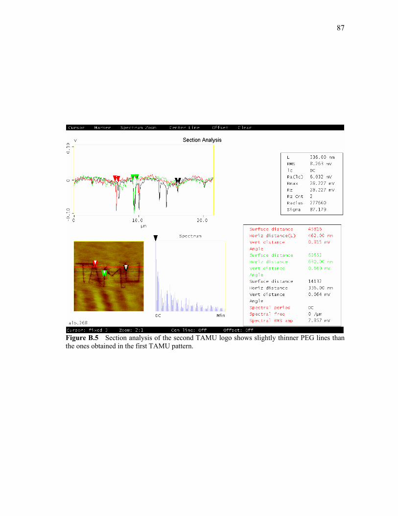
87
Figure B.5 Section analysis of the second TAMU logo shows slightly thinner PEG lines than
the ones obtained in the first TAMU pattern.

88
VITA
Name: Juan Alberto Rivas Cardona
Address: Laguna Verde 1216, Irapuato, Gto., 36631, Mexico.
Email Address: [email protected]
Education: B.S., Mechanical Engineering, Universidad de Guanajuato, Mexico, 2004.
M.S., Mechanical Engineering, Texas A&M University, 2006.
AWARDS
• B.S. degree awarded with Laureate honors, May 2004.
• Scholarship to participate in the Congress of the Eighth Scientific Research Summer of the
University of Guanajuato, July – August 2002.
• 3rd Place in the National Contest of Chemistry organized by the Mexican Academy of
Sciences, Morelia, Mexico, March 1998.
• 1st Place in the State Contest of Chemistry organized by the Public Education Secretariat
(SEP, for its acronym in Spanish), Guanajuato, Mexico, April 1997.
• 2º Place in the National Contest of Chemistry organized by the Mexican Academy of
Sciences Morelos, Mexico, March 1997.
• 1st Place in the State Contest of Electronics organized by the Public Education Secretariat
(SEP, for its acronym in Spanish), Dolores Hidalgo, Mexico, 1995.
PUBLICATIONS
1. A. Rivas-Cardona, D. Banerjee, “Fabrication of a microfluidic device for simultaneous
patterning of multiple chemical species by Dip Pen Nanolithography (DPN™)”,
Proceedings of SPIE Vol. 6223, ISBN: 0-8194-6279-9, June 2006. 2. A. Rivas-Cardona, A. Hernandez-Guerrero, R. Lesso-Arroyo, R. Romero-Mendez, Rosa H.
Chavez, “Efectos de la Radiación en el Enfriamiento de Fuentes muy Intensas de Calor
Contenidas Dentro de un Encajonamiento”, XVI National Congress of Mechanical
Engineering, Leon, Spain, December 2004.
3. A. Rivas-Cardona, A. Hernandez-Guerrero, R. Romero-Méndez and R. Lesso-Arroyo,
“Liquid-Mixed Convection in a Closed Enclosure with Highly-Intensive Heat Fluxes”,
International Journal of Heat and Mass Transfer, 47/19-20 pp. 4089-4099, 2004.
4. A. Rivas-Cardona, A. Hernandez-Guerrero, A. Fuentes-Grimaldi, R. Lesso-Arroyo, R.
Romero-Mendez, “Dissipation Patterns Within an Enclosure Where Several Highly -
Intensive Heat Fluxes Are Placed,” 16th International Conference on Efficiency, Costs,
Optimization, Simulation and Environmental Impact of Energy Systems (ECOS 2003),
Copenhagen, Denmark, July 2003.