development of a multi-channel rgb laser diode …
TRANSCRIPT

DEVELOPMENT OF A MULTI-CHANNEL RGB LASER DIODE DRIVER FOR
LASER PROJECTION APPLICATIONS

DEVELOPMENT OF A MULTI-CHANNEL RGB LASER DIODE DRIVER FOR
LASER PROJECTION APPLICATIONS
By Rong Zha, B.Eng, M.Eng
A Thesis Submitted to the School of Graduate Studies in Partial Fulfillment of the
Requirements for the Degree Master of Applied Science
McMaster University © Copyright by Rong Zha, September 2019.

TITLE: Development of A Multi-channel RGB Laser Diode Driver for
Laser Projection Applications
AUTHOR: Rong Zha,
SUPERVISOR: Prof. Chang-qing Xu
NUMBER OF PAGES: xviii, 150.

M. A. Sc. Thesis – Rong Zha McMaster University – Engineering Physics
i
Abstract
In this thesis, a red green and blue (RGB) laser diode driver (LDD) is designed, assembled
and tested, which can work as a standalone device or an internal component fully controlled
by a laser projector. In particular, the thesis explores a multi-channel RGB LDD for a
retrofitted laser projector, targeting projectors for home, business and education.
If laser diodes (LDs) with the same color are connected in series, a higher forward
voltage is required, making most commercial LDDs unsuitable for this application due to
their insufficient compliance voltages. If the connections of all the LDs are in parallel,
issues on size and cost arise since many LDs are used in this case. Another problem to use
the commercial LDDs for RGB laser projection is that there are no proper communication
interfaces to link the LDDs to the laser projector.
In order to solve these problems by taking advantage of all the features of iC-HTG,
an integrated circuit with automatic current control functionality, both the hardware circuits
and the software for an eight-channel LDD are designed. Experimental results show that
all the RGB channels can achieve compliance voltage of 23 V within the required working
current range, which can drive up to 5 blue, 4 green or 10 red LDs in series in each single
channel. It is confirmed experimentally that the designed LDD can fulfill the requirements
on driving current (i.e. 1% accuracy and 1% stability) .
The protection functions of the developed LDD are also explored and verified
experimentally. It can detect the open laser connection before the LDD channels are
enabled. Fast over-current protection can be achieved within 1.5 µs.

M. A. Sc. Thesis – Rong Zha McMaster University – Engineering Physics
ii
Circuit interfaces and protocols of the communications enable the multi-channel
RGB LDD to work as a standalone device or an internal component of the laser projector.
Key words: RGB laser projector, laser diode driver, iC-HTG, laser diode protection.

M. A. Sc. Thesis – Rong Zha McMaster University – Engineering Physics
iii
Acknowledgement
I would like to thank many people throughout my study at McMaster.
First and foremost, I would to express my special appreciation and deepest gratitude
to my supervisor Prof. Chang-qing Xu for his selfless supports, patient discussions, kind
guidance as well as priceless advices. Here, I sincerely thank to you for your great
encouragement, tolerance and patience during the periods of my study.
I would like to express my sincere gratitude to my committee member: Prof. Adrian
Kitai and Prof. Adriaan Buijs. It is my honor to be a TA for 3BB3 and work with Prof.
Buijs. Special thanks to Prof. Kitai for your SID books and the guidance for my presentation
in the department seminar.
I would like to thank all the colleagues in my group: Fangfang Zhang, Bin Zhang,
Mahmoud Khalil Mahmoud, Yushan Zhang, Jianxi Qu, Tyler Khashak and Joshua Kneller.
Thanks Dr. Qianli Ma for sharing the knowledge about speckles in the lasers.
I would like to thank Dr. Lorraine Liang and Yamn Chalich for the proofreading
and grammar check.
Lastly, but the most importantly, I would like to express my appreciation for my
family, especially for my parents and wife. Thanks to them for their unconditional support
and endless help. Special thanks to my daughter for taking care of her younger brother
when my wife and I are busy.
M. A. Sc. Thesis – Rong Zha McMaster University – Engineering Physics
iv
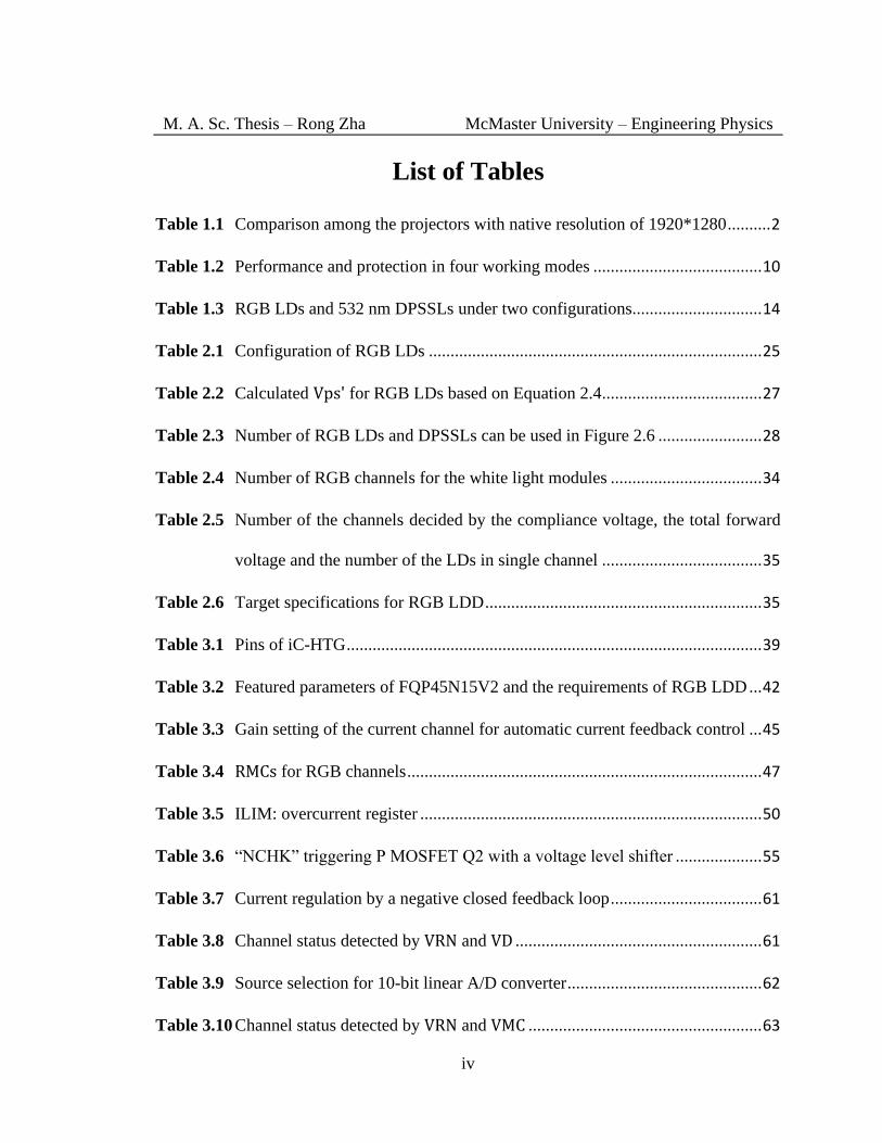
List of Tables
Table 1.1 Comparison among the projectors with native resolution of 1920*1280 .......... 2
Table 1.2 Performance and protection in four working modes ....................................... 10
Table 1.3 RGB LDs and 532 nm DPSSLs under two configurations.............................. 14
Table 2.1 Configuration of RGB LDs ............................................................................. 25
Table 2.2 Calculated Vps' for RGB LDs based on Equation 2.4..................................... 27
Table 2.3 Number of RGB LDs and DPSSLs can be used in Figure 2.6 ........................ 28
Table 2.4 Number of RGB channels for the white light modules ................................... 34
Table 2.5 Number of the channels decided by the compliance voltage, the total forward
voltage and the number of the LDs in single channel ..................................... 35
Table 2.6 Target specifications for RGB LDD ................................................................ 35
Table 3.1 Pins of iC-HTG ................................................................................................ 39
Table 3.2 Featured parameters of FQP45N15V2 and the requirements of RGB LDD ... 42
Table 3.3 Gain setting of the current channel for automatic current feedback control ... 45
Table 3.4 RMCs for RGB channels .................................................................................. 47
Table 3.5 ILIM: overcurrent register ............................................................................... 50
Table 3.6 “NCHK” triggering P MOSFET Q2 with a voltage level shifter .................... 55
Table 3.7 Current regulation by a negative closed feedback loop ................................... 61
Table 3.8 Channel status detected by VRN and VD ......................................................... 61
Table 3.9 Source selection for 10-bit linear A/D converter ............................................. 62
Table 3.10 Channel status detected by VRN and VMC ...................................................... 63

M. A. Sc. Thesis – Rong Zha McMaster University – Engineering Physics
v
Table 3.11 Configuration of I2C address for eight LDD channels .................................... 70
Table 3.12 I2C address for eight LDD channels ............................................................... 70
Table 3.13 I2C commands of reading and writing for the LDD channels ......................... 71
Table 4.1 Parameters for UART: 8E1@9600 bps ........................................................... 84
Table 4.2 UART Commands and requests from the host computer to the MCU ............ 85
Table 4.3 Information echoed from the MCU to the host computer ............................... 86
Table 4.4 Overview of status registers ............................................................................ 88
Table 4.5 Decoding the commands and requests from UART to I2C ............................. 94
Table 5.1 Pass/Fail table for target specifications ......................................................... 124

M. A. Sc. Thesis – Rong Zha McMaster University – Engineering Physics
vi
List of Figures
Figure 1.1 CIE 1931 (x, y) chromaticity diagram of Rec. 709, digital cinema initiative
primary 3 (DCI‐P3), and Rec. 2020 gamut. The symbol “○” indicates the
reference white of Rec. 709 and Rec. 2020 and the symbol “□” indicates the
reference white of DCI‐P3. (Reprinted with permission from [25] Candry,
Patrick, and Bart Maximus. "Projection displays: New technologies,
challenges, and applications." Journal of the Society for Information Display
23.8 (2015): 347-357.) ................................................................................... 4
Figure 1.2 Red module: (a) red LDs, (b) dimensions: 280 mm * 265 mm * 68 mm ...... 4
Figure 1.3 (a) RGB LD package, (b) whole light module with heat-dissipation ((a) and
(b) are reprinted with permission from [31] Nagahara, Seiji. "8‐1: Three
Primary Color LD Module." SID Symposium Digest of Technical Papers.
Vol. 48. No. 1. 2017.) .................................................................................... 6
Figure 1.4 (a) Conceptual laser driver (Reprinted with permission from [40] B. Dobkin,
and J. Williams, “Current sources for fiber optic lasers: A compendium of
pleasant current events,” Analog Circuit Des., pp. 319–337, Jan. 2011.); (b)
Current enters the sink and exits the source ................................................... 7
Figure 1.5 Functional block diagram of an ILX Lightwave precision current source
topology (Adapted from [41]. Permission to use granted by Newport
Corporation. All rights reserved.) .................................................................. 8
Figure 1.6 GPIB connectors .......................................................................................... 11

M. A. Sc. Thesis – Rong Zha McMaster University – Engineering Physics
vii
Figure 1.7 (a) Blue laser phosphor [45], (b) Independent RGB lasers are used for the
primary colors [45] (NEC Display Solutions Europe GmbH ©2019 ) ........ 12
Figure 1.8 Blue laser module ........................................................................................ 13
Figure 1.9 Commercial LDDs for RGB LDs and DPSSLs ........................................... 15
Figure 2.1 P-I curve of green LD, NDG 7475 from Nichia, in the legend of free-running
gain device without temperature information (Reprinted with permission
from [47] Xu, Binbin, et al. "High-power broadly tunable grating-coupled
external cavity laser in green region." Review of Scientific Instruments 89.12
(2018): 125106.) .......................................................................................... 20
Figure 2.2 (a) Temperature dependence of P-I curve for the green LD in CW mode, (b)
temperature dependence of P-I curve for the blue LD in CW mode ((a) and
(b) are reprinted with permission from [26] Murayama, Masahiro, et al.
"Watt‐class green (530 nm) and blue (465 nm) laser diodes." physica status
solidi (a) 215.10 (2018): 1700513.) ............................................................. 21
Figure 2.3 OEM thermal packages for RGB LDs ......................................................... 21
Figure 2.4 Drain current as a function of the drain-to-source voltage and the gate-to-
source bias over the threshold voltage [50] (Permission is granted to copy,
distribute and/or modify this document under the terms of the GNU Free
Documentation License.) ............................................................................. 23
Figure 2.5 A conceptual current sink and its circuit implementation............................ 24
Figure 2.6 A conceptual four-channel LDD with an external power supply ................ 26

M. A. Sc. Thesis – Rong Zha McMaster University – Engineering Physics
viii
Figure 2.7 An eight-channel LDD for RGB LDs .......................................................... 28
Figure 2.8 Block diagram of iC-HTG for the feedback loop path [54] ......................... 30
Figure 2.9 Function block diagram of iC-HTG with a size of 4mm*4mm [54] ........... 31
Figure 2.10 Schematic of the laser diode current driver, which is divided into separate
functions (Reprinted with permission from [55] Erickson, Christopher J., et
al. "An ultrahigh stability, low-noise laser current driver with digital control."
Review of Scientific Instruments 79.7 (2008): 073107.) ............................. 32
Figure 3.1 iC-HTG function diagram with its pin number [54] .................................... 38
Figure 3.2 Pin configuration of iC-HTG ....................................................................... 38
Figure 3.3 (a) Current sink with a low side current sense; (b) current source with a low
side current sense; (c) current source with a high side current sense (d) current
sink with a high side current sense .............................................................. 40
Figure 3.4 Maximum SOA (red) of FQP45N15V2 ....................................................... 43
Figure 3.5 Block diagram of iC-HTG with the controlling flow of the current regulation
...................................................................................................................... 45
Figure 3.6 Current ramping up to 1.8 A without overshoot; VRMC in yellow, VRN in
purple, RMC of 0.3 Ω, CI of 1µF .................................................................. 49
Figure 3.7 P MOSFET crowbar .................................................................................... 51
Figure 3.8 External circuits for triggering the crowbar circuits .................................... 52
Figure 3.9 1.15 µs delay time from OVC event to NCHK output; NCHK in yellow
and VRMC in purple ..................................................................................... 53

M. A. Sc. Thesis – Rong Zha McMaster University – Engineering Physics
ix
Figure 3.10 Schematic and PCB of a voltage level shifter .............................................. 55
Figure 3.11 OVP by MOSFET crowbar circuits, comparator without latching function57
Figure 3.12 Simulation results for OVP in Figure 3.11 .................................................. 57
Figure 3.13 OVP by MOSFET crowbar circuits, comparator with latching function .... 58
Figure 3.14 Simulation results for OVP in Figure 3.13 .................................................. 58
Figure 3.15 Overvoltage due to open connection of LDs ............................................... 60
Figure 3.16 VD and VBL are measured by the ADC inside the iC-HTG ........................ 62
Figure 3.17 A driving circuit for a relay.......................................................................... 66
Figure 3.18 PCB size for the circuits of NUD3124 ........................................................ 67
Figure 3.19 Reverse voltage from an OEM switch mode LDD ...................................... 68
Figure 3.20 Reverse protection by a reversed Schottky diode ........................................ 68
Figure 3.21 A block diagram for the communication interfaces in the RGB LDD ........ 69
Figure 3.22 I2C for eight LDD channels ......................................................................... 71
Figure 3.23 (a) Top and (b) bottom of i6A240 from TDK Lambda................................ 72
Figure 3.24 DC-DC modules ........................................................................................... 73
Figure 3.25 Red LDD channel ........................................................................................ 75
Figure 3.26 Top level diagram of RGB LDD.................................................................. 76
Figure 4.1 Software in the host computer and firmware in the MCU ........................... 78
Figure 4.2 A top-level flowchart for the firmware ........................................................ 79
Figure 4.3 Flowchart of UART ..................................................................................... 80
Figure 4.4 Flowchart of standalone configuration for the RGB LDD .......................... 83
M. A. Sc. Thesis – Rong Zha McMaster University – Engineering Physics
x
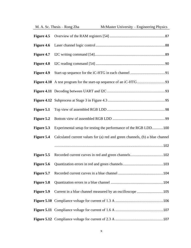
Figure 4.5 Overview of the RAM registers [54] ........................................................... 87
Figure 4.6 Laser channel logic control .......................................................................... 88
Figure 4.7 I2C writing command [54] ........................................................................... 89
Figure 4.8 I2C reading command [54] .......................................................................... 90
Figure 4.9 Start-up sequence for the iC-HTG in each channel ..................................... 91
Figure 4.10 A test program for the start-up sequence of an iC-HTG .............................. 93
Figure 4.11 Decoding between UART and I2C .............................................................. 93
Figure 4.12 Subprocess at Stage 3 in Figure 4.3 ............................................................. 95
Figure 5.1 Top view of assembled RGB LDD .............................................................. 98
Figure 5.2 Bottom view of assembled RGB LDD ........................................................ 99
Figure 5.3 Experimental setup for testing the performance of the RGB LDD............ 100
Figure 5.4 Calculated current values for (a) red and green channels, (b) a blue channel
.................................................................................................................... 102
Figure 5.5 Recorded current curves in red and green channels ................................... 102
Figure 5.6 Quantization errors in red and green channels ........................................... 103
Figure 5.7 Recorded current curves in a blue channel ................................................ 104
Figure 5.8 Quantization errors in a blue channel ........................................................ 104
Figure 5.9 Current in a blue channel measured by an oscilloscope ............................ 105
Figure 5.10 Compliance voltage for current of 1.3 A ................................................... 106
Figure 5.11 Compliance voltage for current of 1.6 A ................................................... 107
Figure 5.12 Compliance voltage for current of 2.3 A ................................................... 107

M. A. Sc. Thesis – Rong Zha McMaster University – Engineering Physics
xi
Figure 5.13 Current stability at 1.3 A in a red channel ................................................. 108
Figure 5.14 Current stability at 1.6 A in a green channel.............................................. 108
Figure 5.15 Current stability at 2.3 A in a blue channel................................................ 109
Figure 5.16 On-off of the power ................................................................................... 110
Figure 5.17 Soft-start of current of 0.9 A ...................................................................... 110
Figure 5.18 Power off a normal channel ....................................................................... 111
Figure 5.19 Power off a saturated channel .................................................................... 111
Figure 5.20 OCP by the iC-HTG within 3 µs................................................................ 112
Figure 5.21 OCP by the iC-HTG in a saturated LDD channel ...................................... 113
Figure 5.22 Crowbar circuits acting under the simulating error events: (a) “SOVC” and
(b) “SOSCERR” ......................................................................................... 114
Figure 5.23 OCP with the crowbar circuits ................................................................... 115
Figure 5.24 OCP with the crowbar circuits in a saturated blue channel (a) clamped current
lasts for 30 ms (b) 1.5 µs overcurrent period ............................................. 116
Figure 5.25 No acknowledgement from the empty Channel 0 ...................................... 117
Figure 5.26 Detection of open laser connection ............................................................ 117
Figure 5.27 Initialization in Channel 4 .......................................................................... 119
Figure 5.28 Initialization in Channel 3 .......................................................................... 119
Figure 5.29 Initialization in Channel 5 .......................................................................... 119
Figure 5.30 A delay of 2 s before the start of I2C communication ............................... 120
Figure 5.31 Command from UART: disable Channel 6 ............................................... 120

M. A. Sc. Thesis – Rong Zha McMaster University – Engineering Physics
xii
Figure 5.32 Command from UART: enable Channel 6 ................................................ 120
Figure 5.33 Command from UART: Changing driving current in Channel 6 .............. 121
Figure 5.34 Command from UART: Changing current limit in Channel 6 .................. 121
Figure 5.35 Request from UART: Request data from address (0x11) in Channel 6..... 121
Figure 5.36 Current of 6 A in the DPSSL channel ........................................................ 122
Figure 5.37 Error in I2C due to the pull-up resistors .................................................... 122
Figure 5.38 Error decoding due to the failure of fetching data from UART................. 123

M. A. Sc. Thesis – Rong Zha McMaster University – Engineering Physics
xiii
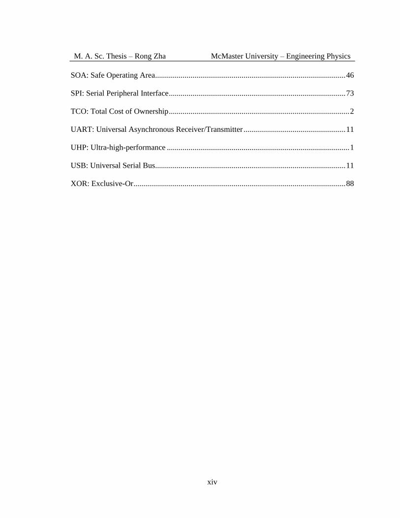
List of Abbreviations and Symbols
AC: Alternating Current .................................................................................................... 23
CES: Consumer Electronics Show....................................................................................... 5
COMD: Catastrophic Optical Mirror Damage .................................................................... 7
DC: Direct current.............................................................................................................. 23
DPSSLs: Diode-Pumped Solid-State Lasers ....................................................................... 4
EMI: Electromagnetic Interference.................................................................................... 24
GPIB: General Purpose Interface Bus ............................................................................... 11
GUI: Graphical User Interface ........................................................................................... 10
HDR: High Dynamic Range ................................................................................................ 2
HID: High-intensity Discharge ............................................................................................ 1
LDD: Laser Diode Driver .................................................................................................... 6
LDs: Laser Diodes ............................................................................................................... 3
LSB: Least Significan Bit ................................................................................................ 105
MCU: Micro-controller Unit.............................................................................................. 17
MOSFET: Metal-Oxide-Semiconductor Field-Effect Transistor ...................................... 24
OCP: Over-Current Protection ........................................................................................... 36
OVP: Over-voltage protection ........................................................................................... 59
PCB: Printed Circuit Board ............................................................................................... 17
PWM: Pulse Width Modulation......................................................................................... 23
QCL: Quantum Cascade Laser .......................................................................................... 19
RGB: Red Green and Blue ................................................................................................... 3
M. A. Sc. Thesis – Rong Zha McMaster University – Engineering Physics
xiv
SOA: Safe Operating Area................................................................................................. 46
SPI: Serial Peripheral Interface .......................................................................................... 73
TCO: Total Cost of Ownership ............................................................................................ 2
UART: Universal Asynchronous Receiver/Transmitter .................................................... 11
UHP: Ultra-high-performance ............................................................................................. 1
USB: Universal Serial Bus................................................................................................. 11
XOR: Exclusive-Or ............................................................................................................ 88

M. A. Sc. Thesis – Rong Zha McMaster University – Engineering Physics
xv
Table of Contents
Abstract ................................................................................................................................. i
Acknowledgement ............................................................................................................. iii
List of Tables ...................................................................................................................... iv
List of Figures ..................................................................................................................... vi
Chapter 1 Introduction ......................................................................................................... 1
1.1 Overview of light sources for projectors .................................................................... 1
1.2 Review of laser drivers ............................................................................................... 6
1.2.1 General requirements for an LDD ....................................................................... 6
1.2.2 Communication interface for the LDD in the projector ...................................... 9
1.2.3 Performance requirements of an RGB LDD in the projector ............................ 11
1.2.4 Protection requirements of an RGB LDD in the projector ................................ 12
1.2.5 Size restrictions for an RGB LDD ..................................................................... 14
1.3 Motivation and objectives of the research ................................................................ 15
1.4 Chapter outline of the thesis ..................................................................................... 16
Chapter 2 Design of a Multi-channel RGB LDD .............................................................. 18
2.1 Benefits of a current sink implemented in linear integrated circuits ........................ 18
2.1.1 Constant current controller ................................................................................ 18

M. A. Sc. Thesis – Rong Zha McMaster University – Engineering Physics
xvi
2.1.2 Linear vs switch ................................................................................................. 22
2.1.3. Discrete vs integrated ....................................................................................... 29
2.2 Design strategy of the RGB LDD for laser projector ............................................... 33
2.3 Target specifications for the RGB LDD .................................................................. 35
2.4 Summary .................................................................................................................. 36
CHAPTER 3 Hardware Design of the RGB LDD ................................................................ 37
3.1 IC-HTG .................................................................................................................... 37
3.2 Performance of the LDD channel ............................................................................. 40
3.2.1 Selection of FQP45N15V2 ................................................................................ 41
3.2.2 Selection of current sense resistors .................................................................... 44
3.3 Design of LD protection ........................................................................................... 47
3.3.1 Soft start and slow turn-on ................................................................................. 47
3.3.2 Overcurrent protection (OCP) by iC-HTG ........................................................ 49
3.3.3 Crowbar protection implemented by MOSFET ................................................ 50
3.3.4 Overvoltage protection ...................................................................................... 55
3.3.5 Shorting relay for ESD protection ..................................................................... 65
3.3.6 Reverse protection ............................................................................................. 67
3.4 Communication interfaces ........................................................................................ 69
3.5 DC-DC module ........................................................................................................ 72

M. A. Sc. Thesis – Rong Zha McMaster University – Engineering Physics
xvii
3.5 Summary .................................................................................................................. 74
CHAPTER 4 Firmware Design for the RGB LDD ............................................................... 77
4.1 Overall design .......................................................................................................... 77
4.2 UART ....................................................................................................................... 84
4.3 LDD channels ........................................................................................................... 86
4.4 Decoding .................................................................................................................. 93
4.5 Protection for the LDs .............................................................................................. 95
4.6 Software in the host computer .................................................................................. 96
4.7 Summary .................................................................................................................. 96
CHAPTER 5 Results and Conclusions ................................................................................. 97
5.1 Experimental setup ................................................................................................... 97
5.2 Experimental results of performance ..................................................................... 100
5.2.1 Accuracy of the driving current ....................................................................... 100
5.2.2 Compliance voltage ......................................................................................... 106
5.2.3 Current stability ............................................................................................... 107
5.3 Experimental results of protection ......................................................................... 109
5.3.1 Tun-on delay and power on-off ....................................................................... 109
5.3.2 OCP by the iC-HTG ........................................................................................ 111
5.3.3 Crowbar circuits............................................................................................... 113
M. A. Sc. Thesis – Rong Zha McMaster University – Engineering Physics
xviii
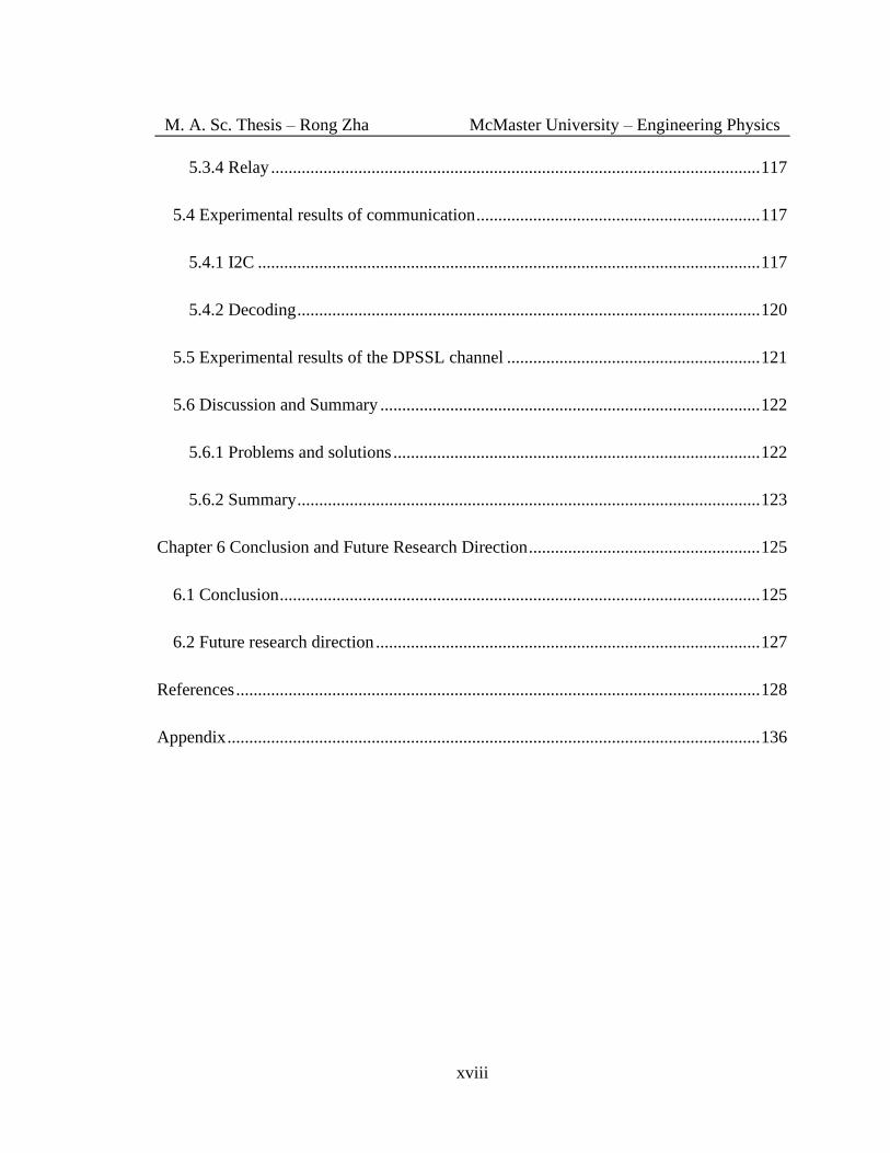
5.3.4 Relay ................................................................................................................ 117
5.4 Experimental results of communication ................................................................. 117
5.4.1 I2C ................................................................................................................... 117
5.4.2 Decoding .......................................................................................................... 120
5.5 Experimental results of the DPSSL channel .......................................................... 121
5.6 Discussion and Summary ....................................................................................... 122
5.6.1 Problems and solutions .................................................................................... 122
5.6.2 Summary .......................................................................................................... 123
Chapter 6 Conclusion and Future Research Direction ..................................................... 125
6.1 Conclusion .............................................................................................................. 125
6.2 Future research direction ........................................................................................ 127
References ........................................................................................................................ 128
Appendix .......................................................................................................................... 136

Chapter 1
Introduction
1.1 Overview of light sources for projectors
Lasers have advantages over other light sources in projection applications since it is well
known that projection is a very demanding application for the light source [1]. Generally
speaking, brightness, color gamut, efficiency and lifetime of the light source restrict this
application [2]. Cost is another crucial factor for a commercial product to be successful on
the market.
Developed from early high-intensity discharge (HID) lamp [3-4], the ultra-high-
performance (UHP) lamp, originally named as ultra-high-pressure lamp [5-6], has been
widely used for projection [7-9] since the specially designed lamp driving electronics was
first invented by Philips [10]. It was capable of driving the UHP to deliver the uniform
screen illumination by generating a short and stable electrical discharging arc inside the
lamp. Although the lifetime of the UHP lamp can exceed 10,000 hours [8], most projector
manufacturers in Table 1.1 indicate lifetime hours of less than 5,000 for the lamp inside the
projectors. These projectors are widely used for home, business and education purpose.
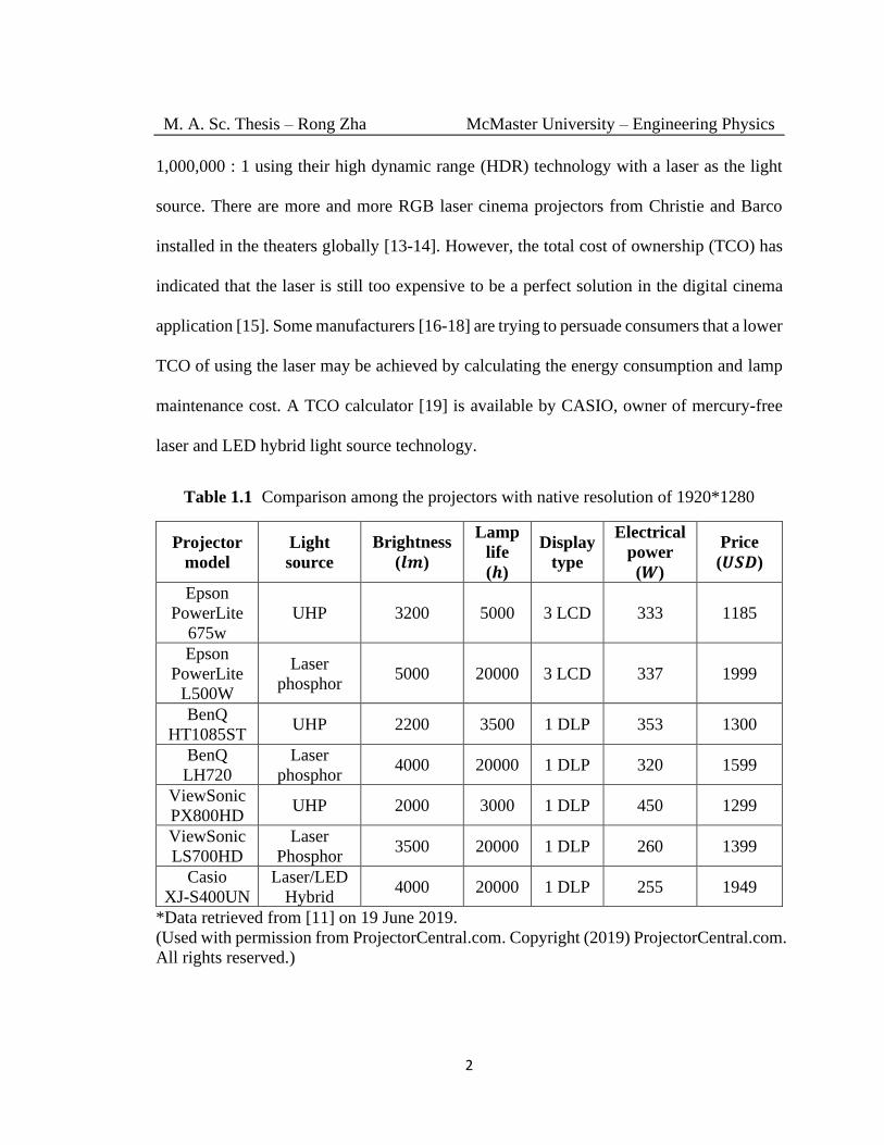
Table1.1 shows that lasers can achieve higher brightness and much longer lifetime
in all display types using less electrical power than the UHP lamps, but the purchasing price
is higher. In fact, their excellent performance including the color gamut has been well
known for decades [12]. Christie teamed with Dolby achieved a contrast ratio of more than
M. A. Sc. Thesis – Rong Zha McMaster University – Engineering Physics
2
1,000,000 : 1 using their high dynamic range (HDR) technology with a laser as the light
source. There are more and more RGB laser cinema projectors from Christie and Barco
installed in the theaters globally [13-14]. However, the total cost of ownership (TCO) has
indicated that the laser is still too expensive to be a perfect solution in the digital cinema
application [15]. Some manufacturers [16-18] are trying to persuade consumers that a lower
TCO of using the laser may be achieved by calculating the energy consumption and lamp
maintenance cost. A TCO calculator [19] is available by CASIO, owner of mercury-free
laser and LED hybrid light source technology.
Table 1.1 Comparison among the projectors with native resolution of 1920*1280
Projector
model
Light
source
Brightness
(𝒍𝒎)
Lamp
life
(𝒉)
Display
type
Electrical
power
(𝑾)
Price
(𝑼𝑺𝑫)
Epson
PowerLite
675w
UHP 3200 5000 3 LCD 333 1185
Epson
PowerLite
L500W
Laser
phosphor 5000 20000 3 LCD 337 1999
BenQ
HT1085ST UHP 2200 3500 1 DLP 353 1300
BenQ
LH720
Laser
phosphor 4000 20000 1 DLP 320 1599
ViewSonic
PX800HD UHP 2000 3000 1 DLP 450 1299
ViewSonic
LS700HD
Laser
Phosphor 3500 20000 1 DLP 260 1399
Casio
XJ-S400UN
Laser/LED
Hybrid 4000 20000 1 DLP 255 1949
*Data retrieved from [11] on 19 June 2019.
(Used with permission from ProjectorCentral.com. Copyright (2019) ProjectorCentral.com.
All rights reserved.)
M. A. Sc. Thesis – Rong Zha McMaster University – Engineering Physics
3
Laser projectors can run at full power for 20,000 hours, roughly 40 hours a week
for a decade, to provide virtually maintenance-free projection [20]. On the other hand, LED,
another lamp-free light source, has lower brightness due to the lower efficiency compared
to the laser [21], which limits its main application within the portable and pocket-size pico-
projector [22].
It is widely accepted that the laser is going to be the dominant light source for the
projection soon [23]. However, most off-the-shelf laser projectors, excluding the ones used
in the cinema theatre, do not directly install red, green and blue (RGB) laser diodes (LDs)
as their primary colors to output the merged white light. According to ITU-R
Recommendation BT.2020 [24], commonly known as Rec. 2020, green light at a
wavelength of 532 nm can offer the best color gamut, as seen in Figure 1.1 [25].
Unfortunately, one of the most challenging tasks is to obtain the green wavelength from a
compact solid-state LD.
Currently, there are no commercial LDs that can provide this wavelength with
sufficient output power. There was a report from Sony about their 530 nm LD which could
achieve 2 W optical output in 2017 [26]. Earlier, Nichia also reported the breakthrough
success in 1-Walt-class 532 nm green LD in 2015 [27]. But no such products are yet
commercially available. High power 532 nm diode pumped solid state lasers (DPSSLs) in
the integrated packages are more expensive and oversized for the general projection
application. Another issue is the size of the assembly for the light modules. Even a
customized 20 W optical module of red LDs in Figure 1.2 is not easily embedded in a
projector due to the excessive volume of the assembly package.

M. A. Sc. Thesis – Rong Zha McMaster University – Engineering Physics
4
Figure 1.1 CIE 1931 (x, y) chromaticity diagram of Rec. 709, digital cinema initiative
primary 3 (DCI‐P3), and Rec. 2020 gamut. The symbol “○” indicates the
reference white of Rec. 709 and Rec. 2020 and the symbol “□” indicates
the reference white of DCI‐P3. (Reprinted with permission from [25]
Candry, Patrick, and Bart Maximus. "Projection displays: New technologies,
challenges, and applications." Journal of the Society for Information
Display 23.8 (2015): 347-357.)
(a) (b)
Figure 1.2 Red module: (a) red LDs, (b) dimensions: 280 mm * 265 mm * 68 mm

M. A. Sc. Thesis – Rong Zha McMaster University – Engineering Physics
5
In the above paragraphs, it was demonstrated that an alternative technology is
necessary to pave the way for manufacturing compact laser projectors at a reasonable price.
Blue LDs have achieved significant advancement during the past two decades [28].
Commercial laser projectors have developed different configurations for the blue laser
phosphor approach to output the white light. Table 1.1 above also shows the light source in
these laser projectors is based on the blue laser phosphor technology. Casio adds the red
LEDs to this blue laser phosphor structure to boost the color quality. However, the white
light generated from laser phosphor suffers from not only the luminance saturation due to
the thermal and optical factors, but also the poor uniformity caused by the backscattered
light [29].
Technology is an evolutionary process. At Consumer Electronics Show (CES) 2019,
Hisense showed an RGB laser “TV”, which was a short throw laser projector with a screen,
and it will not be available in the market until late in 2019 [30]. Nichia introduced the three-
primary color RGB LD module embedded in a compact package shown in Figure 1.3,
which dramatically reduced the volume of the optical module. However, this module can
not fully conform to Rec.2020 color space due to the different green wavelength. It is still
very impressive for its output brightness of over 2000 lumen at around 6500 K [31]. With
the development of the technology in the green laser diode as well as the reduced package
size, pure RGB LDs at a lower cost will be expected to be used more frequently in common
projectors. As a result, different driving electronics for the specific configurations for RGB
LDs are required.

M. A. Sc. Thesis – Rong Zha McMaster University – Engineering Physics
6
The following review will examine the problems in the current laser diode driver
(LDD) for the projector application.
Figure 1.3 (a) RGB LD package, (b) whole light module with heat-dissipation ((a) and
(b) are reprinted with permission from [31] Nagahara, Seiji. "8‐1: Three
Primary Color LD Module." SID Symposium Digest of Technical Papers.
Vol. 48. No. 1. 2017.)
1.2 Review of laser drivers
1.2.1 General requirements for an LDD
Despite all the merits discussed above, sensitivity to the operation environment is a
well-known issue for the LDs [32]. These delicate devices are easily damaged by electro-
static discharge [33-37], excessive current levels [38] and power-on-off transient [39].
Above the lasing threshold, the output optical power is proportional to the injected current
while the forward voltage is almost constant. The most important feature is the output
optical power responds to the driving current extremely quickly. Consequently, the LD can
be damaged even with a very short duration of current spike in the driving circuits since
the burst of optical power caused by the current spike can melt down the facets on the LD.
In other words, LDs are fragile for catastrophic optical mirror damage (COMD) induced

M. A. Sc. Thesis – Rong Zha McMaster University – Engineering Physics
7
by overcurrent events. Therefore, there are two basic requirements for a general LDD:
performance and protection [40].
Figure 1.4 (a) describes the basic requirements for the performance of an LDD,
including:
1) Constant current closed-loop regulator (represented by the two crossed circles in
the middle);
2) Output current controlled by input voltage, i.e., V-I converter;
3) Adjustable clamping input for the maximum output current;
4) Optional output enable function.
It can be a voltage controlled current source or sink based on the direction of current
as shown in Figure 1.4 (b). Performance also concerns output restrictions, such as
compliance voltage, (i.e., maximum voltage range for outputting the constant current),
efficiency, as well as the stability of the current magnitude.
(a) (b)
Figure 1.4 (a) Conceptual laser driver (Reprinted with permission from [40] B. Dobkin,
and J. Williams, “Current sources for fiber optic lasers: A compendium of
pleasant current events,” Analog Circuit Des., pp. 319–337, Jan. 2011.); (b)
Current enters the sink and exits the source

M. A. Sc. Thesis – Rong Zha McMaster University – Engineering Physics
8
On the other hand, laser driver manufacturer ILX Lightwave, now with Newport
Corporation, listed the essential protection features embedded in Figure 1.5 for their
product as follows [41].
1) Soft start for suppressing the power-on transient;
2) Clamping current limit for the closed loop regulation of current;
3) Shorting relay across the laser diode for ESD protection during the power off period;
4) Over-voltage protection for the laser diode
Figure 1.5 Functional block diagram of an ILX Lightwave precision current source
topology (Adapted from [41]. Permission to use granted by Newport
Corporation. All rights reserved.)
These protection components aim to prevent damage to the LD from bad
mechanical connections as well as electrical issues. The intermittent contact between the
LD and the LDD could be caused by the mechanical overstress of the cables [41] or the
vibration of the interface. In this case, the LD will overshoot immediately if the closed
connection is restored from the open condition without the over-voltage protection.

M. A. Sc. Thesis – Rong Zha McMaster University – Engineering Physics
9
Practically, this voltage is limited to the power supply voltage, still higher than the forward
voltage across the LD. Eventually, the current will be regulated to the setting value by the
negative feedback inside the closed loop as shown in Figure 1.5. However, an overshoot of
micro-seconds duration can damage the LD [42]. Therefore, the over-voltage protection
must disable and latch the output of the LDD before the overcurrent happens.
Detailed discussion for the theory and the implementation of the circuits will be
included in Chapter 2.
1.2.2 Communication interface for the LDD in the projector
In the case of projection application, besides the performance and the protection
discussed above, hand-shaking communications between the projector main electronics and
LDD circuits are necessary for at least four different working modes as listed in Table 1.2.
Main electronics of the projector initiates the communication as a “master”, while the LDD
circuits echoes the response as a “slave” based on the predefined protocol. This is a
universal requirement for the driving circuits of the light source in a projector regardless
the choice of the laser or the lamp.
Therefore, an easy-to-use hardware interface for the communications should be
included in the customized LDD circuits. Otherwise, issues for directly using the LDD can
be raised. Most commercial LDDs do not see the communication interface as an essential
component because they provide the mechanical knobs and buttons at the front panel for
the configuration and adjustment. High-end LDDs from IXL-Lightwave can be controlled
by the software, a graphical user interface (GUI), in the host computer via their

M. A. Sc. Thesis – Rong Zha McMaster University – Engineering Physics
10
communication interface like the General Purpose Interface Bus (GPIB) [43] in Figure 1.6.
However, this interface is too complicated for the projector hardware and protocol software.
Its hardware uses too many input and output pins for the communication and the GUI is
based on the very resource-demanding software from LabVIEW [44]. Moreover, Even the
LDD with a Universal Serial Bus (USB) to Universal Asynchronous Receiver/Transmitter
(UART) interface is not suitable for the projector. This is because these communication
interfaces are designed for the host computers. The typical performance of the controller in
the projector is much lower than the CPU in the computer.
Table 1.2 Performance and protection in four working modes
Working
mode Performance Protection
Start up Sending controlling commands and
request the status of LDs
Disable the light output if the
faulty in the laser is detected
Normal Monitoring the thermal and electrical
status of the LDs
Overcurrent, overvoltage,
overheat
Eco & standby Decrease/disable the driving current Overvoltage, overheat
Wake up Increase/enable the driving current to
the normal status
Overcurrent, overvoltage,
overheat

M. A. Sc. Thesis – Rong Zha McMaster University – Engineering Physics
11
Figure 1.6 GPIB connectors
Unlike well-established communication protocols between the light source driving
circuits and the projector controlling circuits in the lamp-based system, no reports are
available yet about the communication protocol between the LDD and the main circuits in
the RGB laser projector.
1.2.3 Performance requirements of an RGB LDD in the projector
Requirements for the performance of the LDD for an RGB laser projector are more
stringent than a commercial laser phosphor projector. The problem is rooted in the
difference of the generation of the primary RGB light illustrated in Figure 1.7 [45] (Laser
in the figure is the module of LDs, not a single LD). A simple way to examine this problem
is to output the pure white light. In the case of blue laser phosphor, fluctuation in the driving
current only affects the output brightness, because the RGB ratio is determined by the
optical elements such as a phosphor wheel and a color wheel. On the other hand, variation

M. A. Sc. Thesis – Rong Zha McMaster University – Engineering Physics
12
of driving current in the RGB channels of LDD will change not only the brightness but also
the RBG color ratio, thus shifting color temperature.
(a) (b)
Figure 1.7 (a) Blue laser phosphor [45], (b) Independent RGB lasers are used for the
primary colors [45] (NEC Display Solutions Europe GmbH ©2019 )
Besides the performance, the following case study will illuminate the unique
protection feature from the RGB LDD inside the projector.
1.2.4 Protection requirements of an RGB LDD in the projector
Protection feature of LDD is highly related to the configuration and the connection
of the LDs.
The application decides the requirements for the protection. On the one hand, Figure
1.8 shows the electrical connection inside one blue light module under the configuration of
laser phosphor. There are two blue modules for the laser projectors listed in Table 1.1. In
the case one string of laser diodes fails, manufacturers declare their products will still work
due to the redundancy provided by the multiple parallel connection of the LD strings.

M. A. Sc. Thesis – Rong Zha McMaster University – Engineering Physics
13
Therefore, the simple way to migrate the protection feature from general LDD to this
configuration is to raise the over-voltage protection limit for each LD string to four times
as high as one LD. This is because the current will not change in the string, while the
forward voltage increases proportional to the number of LDs in series.
Figure 1.8 Blue laser module
On the other hand, an RGB LDD has two different scenarios. One case is for the
digital cinema application where there are large quantities of LDs for each primary RGB
color. In this case, it can also take advantage of this redundancy by adopting a similar
structure for each color. However, it will suffer from a slight color temperature shift in case
one string is damaged, or it will sacrifice a small ratio of the brightness to maintain the
color ratio by reducing the power of normal LDs in other colors accordingly. The other
case is for fewer RGB LDs as in our application. Table 1.3 lists two configurations for RGB
LDs and DPSSLs in the conducted research in the early stages. If five blue LDs are
connected in a string and only one blue LD is shorted, the output brightness will be reduced
to 80% in order to keep the color ratio. Such brightness loss is not acceptable for projection.
In the worst case, damage in open circuit will cause no output light.

M. A. Sc. Thesis – Rong Zha McMaster University – Engineering Physics
14
Table 1.3 RGB LDs and 532 nm DPSSLs under two configurations
R: 637 nm G 520 nm / 532 nm B 460 nm
1# 20 12 5
2# 20 8 LD + 2 DPSSL 5
If an LDD drives one LD, the damage of the LD only affects itself. Conversely, if
an LDD drives many RGB LDs in the projection, the damage of one LD affects
performance slightly but the whole system can still survive due to sufficient redundancy.
Since we do not have enough redundancy in our LDs (particularly the blue LDs), protection
is especially important in our application.
Section 2.2 will explain the pros and cons for the different connections of LDs for
this case in details. The choice is made upon the consideration of the trade-offs between
the performance and the protection.
1.2.5 Size restrictions for an RGB LDD
Three customized LDDs for the RGB LDs used in the first prototype are on the top
of the 19-inch rack as shown in Figure 1.9. Size matters if the LDDs need to be embedded
in the projector. An integrated LDD capable of driving RGB LDs in a small form factor is
necessary.
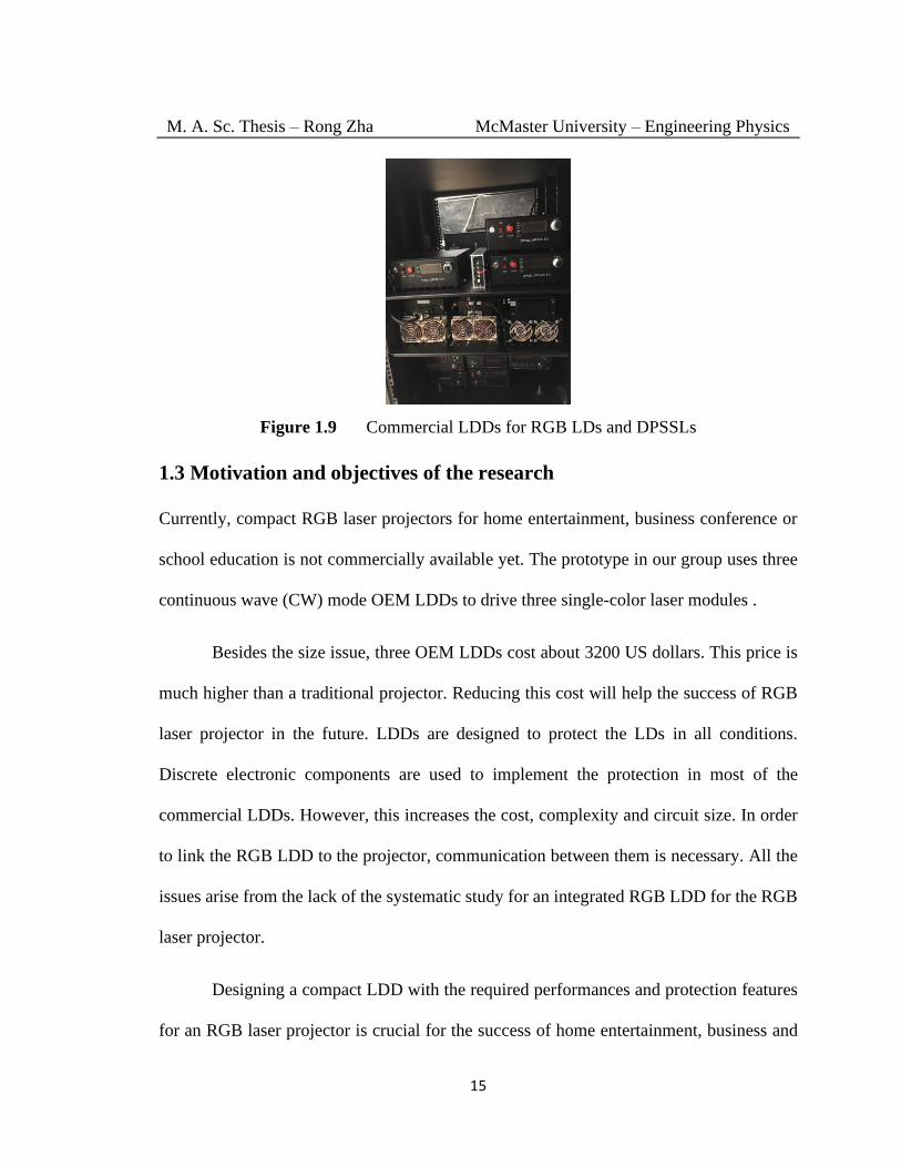
M. A. Sc. Thesis – Rong Zha McMaster University – Engineering Physics
15
Figure 1.9 Commercial LDDs for RGB LDs and DPSSLs
1.3 Motivation and objectives of the research
Currently, compact RGB laser projectors for home entertainment, business conference or
school education is not commercially available yet. The prototype in our group uses three
continuous wave (CW) mode OEM LDDs to drive three single-color laser modules .
Besides the size issue, three OEM LDDs cost about 3200 US dollars. This price is
much higher than a traditional projector. Reducing this cost will help the success of RGB
laser projector in the future. LDDs are designed to protect the LDs in all conditions.
Discrete electronic components are used to implement the protection in most of the
commercial LDDs. However, this increases the cost, complexity and circuit size. In order
to link the RGB LDD to the projector, communication between them is necessary. All the
issues arise from the lack of the systematic study for an integrated RGB LDD for the RGB
laser projector.
Designing a compact LDD with the required performances and protection features
for an RGB laser projector is crucial for the success of home entertainment, business and

M. A. Sc. Thesis – Rong Zha McMaster University – Engineering Physics
16
school education applications. As discussed above, no commercial product can fulfill these
demands yet. Therefore, it is of great interest to develop this LDD to accelerate the
development of the RGB laser projector.
The thesis focuses on the CW mode LDD for the RGB lasers in a light valve
projector. Laser scanning projectors are excluded in the discussion.
1.4 Chapter outline of the thesis
This thesis is organized into 6 chapters. The first chapter begins with the advantage of the
laser as the light source in the projector. It is followed by a brief review of general LDD
and the requirements of performance and protection features due to the LDs of different
connections in the projection application.
Based on the theoretical background for the LDD, Chapter 2 details all the
performance and protection requirements to form a design strategy to fulfill all the demands.
As a result, a table of all the target specifications will be presented.
Chapter 3 provides the hardware design with detailed circuits to fulfill the
specifications. This includes the selection of the power MOSFETs and current sense
resistors based on the performance requirements; implementation of the protecting function
in a minimum hardware cost by exploitation of the internal resources of iC-HTG; and two
communication interfaces: one inside the RGB LDD circuits, and the other connecting the
driving circuits to the motherboard of the projector. The advantage of using iC-HTGs from
iC-haus company to build these interfaces can not only significantly decrease the size of
circuits, but also enable the analog driving circuits to be controlled digitally without extra

M. A. Sc. Thesis – Rong Zha McMaster University – Engineering Physics
17
cost. The circuit schematic and the print circuit board (PCB) are also included in this
chapter.
Chapter 4 focuses on the embedded firmware for RGB LDD, which can be executed
in a commercial micro-controller unit (MCU). The firmware is mainly for the
communication between the projector and RGB LDD as well as the decoding and
communication inside the RGB LDD. Moreover, a protocol to mimic the behaviour of the
projector in the UART communication is introduced and implemented in this part for the
first time. The protection function implemented in this chapter relies on the firmware to
detect the open laser connection and the saturation of the current in the channel.
Chapter 5 discusses the experimental results for the completed design. Results of
this prototype will be analyzed to prove that the performance and protection of the LDD
meet the specifications in Chapter 2.
The final chapter concludes the thesis and predicts the outlook of future LDDs in
RGB laser projectors.

M. A. Sc. Thesis – Rong Zha McMaster University – Engineering Physics
18
Chapter 2
Design of a Multi-channel RGB LDD
There are various LDDs available on the market. Some are for driving high power pumping
LDs with the current of more than 10A . Some feature low-noise current, which is required
for achieving narrow-linewidth emission. Most LDDs have only one output channel for a
single LD with typical compliance voltage under 15V, because the maximum voltage of a
Quantum Cascade Laser (QCL) is between 5V and 14V, which has the highest voltage
among all the LDs.
The requirements for the LDDs in RGB laser projectors make all the off-the-shelf
LDDs unsuitable. Section 2.1 explains the reasons for choosing an integrated linear RGB
LDD. Section 2.2 outlines a design strategy based on optical module requirements. It helps
to reduce the number of channels in the RGB LDD to six. Finally, Section 2.3 lists the
target specifications for the RGB LDD.
2.1 Benefits of a current sink implemented in linear integrated circuits
To explore these benefits, two detailed comparisons are made after the introduction of
characteristics of the RGB LDs in this section.
2.1.1 Constant current controller
It is natural to study the characteristics of the loads before you design the driving circuits
for them. In this research project, RGB LDs and DPSSLs of 532 nm will eventually be used
in the projection, although the DPSSLs will use commercial drivers in Phase one of the

M. A. Sc. Thesis – Rong Zha McMaster University – Engineering Physics
19
project. Unfortunately, only one datasheet of red LD (HL63283HD from USHIO) is
available [46]. According to the datasheet, the optical output power versus forward current
(P-I or L-I) curve for the red LD is linear beyond the threshold of the lasing value. But its
efficiency suffers from the rising temperature. In the case of injecting forward current of 1
A, the optical output power at 45 °C dramatically drops to half of the power at 0 °C.
Therefore, it is necessary to keep thermal stability of the red LDs to maintain the linear
regulation of the optical power by the driving current.
Nichia does not offer the datasheets of the specific green and blue LDs used in our
research. However, there are two reports [47-48] with the P-I curves for the green LD
(NDG7475 from Nichia) in Figure 2.1 and the blue LD (NDB7A75 from Nichia)
respectively. These curves are similar to the P-I curve of the red LD. The output optical
power can be linearly regulated by the driving current above the lasing threshold. On the
other hand, Nichia released the temperature dependence charts in Figure 2.2 for their green
and blue LDs [26]. Unlike the red LD, the green and blue LDs are not sensitive to the
temperature.
An LD is inherently a current-driven device according to its P-I curve. As a result,
an LDD should be capable of regulating the current, i.e., a constant current controller.
“Constant current” does not mean the current can not be adjusted. A constant current driver
and a voltage source are the two sides of a coin. In fact, it specifies that the output voltage
follows the change of the load, while the current maintain its value in contrary to the
concept of the (constant) voltage source.

M. A. Sc. Thesis – Rong Zha McMaster University – Engineering Physics
20
Figure 2.1 P-I curve of green LD, NDG 7475 from Nichia, in the legend of free-running
gain device without temperature information (Reprinted with permission
from [47] Xu, Binbin, et al. "High-power broadly tunable grating-coupled
external cavity laser in green region." Review of Scientific Instruments
89.12 (2018): 125106.)
Our group designed the heatsinks for the optical modules based on the efficiency of
the LDs. Stable temperature for all the LDs is achieved by the extruded aluminum heatsinks
with fans and combined with the aluminum and copper heat conductor wrapped around
each LD by an OEM factory as shown in Figure 2.3, which provides enough redundancy
for dissipating the heat generated by the LDs. A similar structure was used and verified in
the previous prototype.

M. A. Sc. Thesis – Rong Zha McMaster University – Engineering Physics
21
(a) (b)
Figure 2.2 (a) Temperature dependence of P-I curve for the green LD in CW mode, (b)
temperature dependence of P-I curve for the blue LD in CW mode ((a) and
(b) are reprinted with permission from [26] Murayama, Masahiro, et al.
"Watt‐class green (530 nm) and blue (465 nm) laser diodes." physica status
solidi (a) 215.10 (2018): 1700513.)
Figure 2.3 OEM thermal packages for RGB LDs

M. A. Sc. Thesis – Rong Zha McMaster University – Engineering Physics
22
On the other hand, each commercial DPSSL came with a pre-tuned TEC controller
embedded in its LDD that recorded the best temperature for the DPSSL. In the thesis, we
will design an LDD channel to demonstrate the capability of providing the specified current
for the DPSSL. Tuning the temperature for the pumping LD to achieve the best
performance of the DPSSL is beyond the scope of this thesis.
2.1.2 Linear vs switch
Different LDDs can be categorized by their input stage types and output stage types [49].
This Section lists these types and aims to find the best solution for our application.
There are two types of inputs, alternating current (AC) input and direct current (DC)
input. An LDD with an AC input contains a very bulky transformer and an electromagnetic
interference (EMI) filter. The size can hardly be reduced to a compact form. Moreover, it
is unnecessary to include AC/DC components in an LDD for projection application. As
each projector has an AC/DC power supply module. On the other hand, LDDs with DC
input varies in the range of input voltage, typically within the range from 5 V to 24 V.
Power supply modules are very cost-effective and well-developed in this range. Therefore,
the developers of LDD with DC input can focus on the current regulating performance and
the protecting methods for the LDs without putting effort into designing an AC/DC power
supply converter.
There are two types of LDDs in the output stage: switch mode and linear mode. The
former one takes advantage of the pulse width modulation (PWM) by varying the duty
cycles in the switching operation of a metal-oxide-semiconductor field-effect transistor

M. A. Sc. Thesis – Rong Zha McMaster University – Engineering Physics
23
(MOSFET). These switching actions happen in the linear region of the MOSFET as shown
in Figure 2.4, where the voltage drops to near zero across the MOSFET. Hence it can
achieve higher efficiency at the cost of a complicated design with more components.
However, it has inherent switching ripple and high frequency noise in the output. Moreover,
it may radiate electromagnetic interference (EMI) which might be an issue for the LDs.
Linear mode features a lower noise output with a simpler structure. But it may suffer from
the lower efficiency as its MOSFET works in the saturation region as shown in Figure 2.4,
where it generates heat due to the simultaneous occurrence of the voltage and the constant
current across the drain and the source.
Figure 2.4 Drain current as a function of the drain-to-source voltage and the gate-to-
source bias over the threshold voltage [50] (Permission is granted to copy,
distribute and/or modify this document under the terms of the GNU Free
Documentation License.)
In order to analyze the LDD in the linear mode, a conceptual linear current sink will
be explored. Current regulation is implemented by the feedback circuits with operational
amplifiers and comparators inside the rectangle as shown in in Figure 2.5, which forces 𝑉𝑠
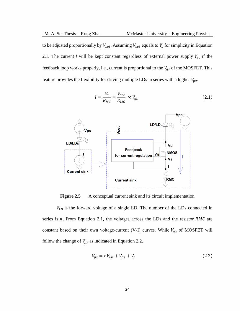
M. A. Sc. Thesis – Rong Zha McMaster University – Engineering Physics
24
to be adjusted proportionally by 𝑉𝑠𝑒𝑡, Assuming 𝑉𝑠𝑒𝑡 equals to 𝑉𝑠 for simplicity in Equation
2.1. The current 𝐼 will be kept constant regardless of external power supply 𝑉𝑝𝑠 if the
feedback loop works properly, i.e., current is proportional to the 𝑉𝑔𝑠 of the MOSFET. This
feature provides the flexibility for driving multiple LDs in series with a higher 𝑉𝑝𝑠.
𝐼 =𝑉𝑠
𝑅𝑀𝐶=
𝑉𝑠𝑒𝑡
𝑅𝑀𝐶 ∝ 𝑉𝑔𝑠 (2.1)
Figure 2.5 A conceptual current sink and its circuit implementation
𝑉𝐿𝐷 is the forward voltage of a single LD. The number of the LDs connected in
series is 𝑛 . From Equation 2.1, the voltages across the LDs and the resistor 𝑅𝑀𝐶 are
constant based on their own voltage-current (V-I) curves. While 𝑉ⅆ𝑠 of MOSFET will
follow the change of 𝑉𝑝𝑠 as indicated in Equation 2.2.
𝑉𝑝𝑠 = 𝑛𝑉𝐿𝐷 + 𝑉ⅆ𝑠 + 𝑉𝑠 (2.2)

M. A. Sc. Thesis – Rong Zha McMaster University – Engineering Physics
25
𝜂 denotes the efficiency of the current sink, assuming the current only passes along
the arrow line as shown in Figure 2.5. From Equation 2.3, if 𝑉𝑝𝑠 increases much higher
than the voltage across the LDs, the efficiency of the current sink will be reduced. In fact,
MOSFET works as a variable resistor of 𝑅𝑁𝑀𝑂𝑆 in the saturation region as shown in Figure
2.4 and Equation 2.3. As a result, increasing 𝑉𝑝𝑠 will increase the equivalent resistance of
𝑅𝑁𝑀𝑂𝑆. Because the current is constant, it will generate extra heat to be dissipated by the
MOSFET. In the extreme cases, the PN junction inside the MOSFET will fail due to the
temperature rising above its limit.
𝜂 =𝑛𝑉𝐿𝐷𝐼
𝑉𝑝𝑠𝐼=
𝑉𝑝𝑠 − 𝑉ⅆ𝑠 − 𝑉𝑠
𝑉𝑝𝑠=
𝑉𝑝𝑠 − 𝐼(𝑅𝑀𝐶 + 𝑅𝑁𝑀𝑂𝑆)
𝑉𝑝𝑠 (2.3)
Generally, efficiency is the major limiting factor in the linear mode. Using more
LDs and reducing 𝑉𝑝𝑠 can achieve a higher efficiency, but an electronic designer of the
LDD cannot change the configuration of the optical modules to be used. Therefore, the
solution is to optimize 𝑉𝑝𝑠 for the current sinks with the given configuration of RGB LDs.
Table 2.1 lists the specifications for RGB LDs used in the projector. 𝐼𝑙𝑖𝑚𝑖𝑡 is the
absolute maximum rating for the forward current. 𝑉𝑚𝑖𝑛 , 𝑉𝑡𝑦𝑝 and 𝑉𝑚𝑎𝑥 represent the
minimum, typical and maximum forward voltage values of the LDs. Unfortunately, not all
the information is available from the manufactures’ datasheets.
Table 2.1 Configuration of RGB LDs
Red: HL63283HD Green:
NDG7475
Blue:
NDB7A75 DPSSL
Number 20 8 5 2

M. A. Sc. Thesis – Rong Zha McMaster University – Engineering Physics
26
𝑉𝑚𝑖𝑛 (V) TBD TBD 3.7 @𝐼𝑡𝑦𝑝 2.0
𝑉𝑡𝑦𝑝 (V) 2.3 @𝑃𝑜_𝑡𝑦𝑝 4.6 @𝐼𝑡𝑦𝑝 TBD TBD
𝑉𝑚𝑎𝑥 (V) 2.7 @𝑃𝑜_𝑡𝑦𝑝 TBD 5.2 @𝐼𝑡𝑦𝑝 2.3
𝐼𝑡𝑦𝑝 (A) 1.3 @𝑃𝑜_𝑡𝑦𝑝 1.5 2.3 TBD
𝐼𝑙𝑖𝑚𝑖𝑡 (A) 1.6 1.8 3.0 5.5
𝑃𝑜_𝑡𝑦𝑝 (W) 1.2 1.0 3.5 TBD
In order to calculate the optimal external power supply 𝑉𝑝𝑠
′, replace conceptual
𝑅𝑁𝑀𝑂𝑆 with its minimum value of 𝑅ⅆ𝑠𝑜𝑛 (40 mΩ) for FPQ45N15V2 [51]. The
resistance 𝑅𝑀𝐶 of the resistor 𝑅𝑀𝐶 is decided by 𝑉𝑠 and 𝐼 . 𝑉𝑠 of less than 0.55 V is
required for the calculation in Equation 2.4. Detailed information regarding this value of 𝑉𝑠
will be analyzed in Inequation 3.8 in Section 3.2.2. The reason of choosing FPQ45N15V2
is explained in Section 3.2.1. Equation 2.4 is used for the calculation for the external power
supply 𝑉𝑝𝑠′ as shown in Figure 2.6. The results are shown in Table 2.2.
𝑉𝑝𝑠 ≥ 𝑛𝑉𝑙ⅆ + 𝐼(𝑅𝑀𝐶 + 𝑅ⅆ𝑠𝑜𝑛) = 𝑛𝑉𝑙ⅆ + 𝑉𝑠 + 𝐼𝑅ⅆ𝑠𝑜𝑛 = 𝑉𝑝𝑠′ (2.4)
Figure 2.6 A conceptual four-channel LDD with an external power supply

M. A. Sc. Thesis – Rong Zha McMaster University – Engineering Physics
27
Table 2.2 Calculated 𝑉𝑝𝑠′ for RGB LDs based on Equation 2.4
Red:
HL63283HD
Green:
NDG7475
Blue:
NDB7A75 DPSSL
Number 20 8 5 2
RMC (mΩ) 300 300 200 100
Vps′@Vmin
(V) TBD TBD 20.1 @Ityp TBD
Vps′@Vtyp
(V) 47.0 @Ityp 40.0 @Ityp TBD <7.8
Vps′@Vmax
(V) 55.0 @Ityp TBD 27.6 @Ityp TBD
As shown in Figure2.6, all the channels share same 𝑉𝑝𝑠′. If we choose 55 V for 𝑉𝑝𝑠′,
about 277 W and 83 W heat will be dissipated by the MOSFET in the DPSSL channel and
blue channel respectively. If the total thermal resistance is as low as 2 °C/W from the PN
junction inside the MOSFET to the ambient temperature, no single MOSFET can survive
because the maximum PN-junction temperature is typically under 170 °C.
Fortunately, Figure 2.7 solves this problem for all the configurations listed in Table
2.3. Two red channels, two green channels and one blue channel are directly connected to
a power supply of +24 V, which is widely available and cost effective on the market. Three
DC/DC converters are used to change +24 V to the proper voltage levels for a DPSSL
channel, a second blue channel and a third red channel respectively. Another benefit to use
+24 V is that the integrated circuit chip, iC-HTG, inside the current sink, can directly use
this voltage source.

M. A. Sc. Thesis – Rong Zha McMaster University – Engineering Physics
28
Figure 2.7 An eight-channel LDD for RGB LDs
As shown in Figure 2.7, a power supply of +24 V with three DC/DC converters
offers more flexibility for testing different optical configurations listed in Table 2.3. This
flexibility is required in the early stage of this research project, when configuration of the
optical modules keeps changing. If the number of the RGB LDs is fixed, selected channels
with or without DC/DC converters can be used in a specific application. The number of
channels to be used in our application will be discussed in Section 2.2.
Table 2.3 Number of RGB LDs and DPSSLs can be used in Figure 2.6
Red:
HL63283HD
Green:
NDG7475 Blue: NDB7A75 DPSSL
Number
@𝑃𝑜_𝑡𝑦𝑝
1-30 @𝑉𝑡𝑦𝑝
1-24 @𝑉𝑚𝑎𝑥
1-10 @𝑉𝑡𝑦𝑝
1-8 @(𝑉𝑡𝑦𝑝+1)
1-12 @𝑉𝑚𝑖𝑛
1-8 @𝑉𝑚𝑎𝑥
1-10 @𝑉𝑚𝑖𝑛
1-9 @𝑉𝑚𝑎𝑥
Obviously, without DC/DC, the green channel may suffer from the low efficiency
with fewer LDs. In the extreme case only one green LD is used, 28.7 W (𝑃𝐹𝑃𝑄) heat will
be generated from the MOSFET FPQ45N15V2 based on the calculation in Equation 2.5.

M. A. Sc. Thesis – Rong Zha McMaster University – Engineering Physics
29
The temperature of 106 °C in the PN-junction (𝑇𝑃𝑁_𝐹𝑃𝑄) inside this MOSFET is below the
limitation of 150 °C base on the calculation in Equation 2.6, with an ambient temperature
20 °C (𝑇𝑎𝑚𝑏𝑖𝑒𝑛𝑡) and a practical total thermal resistance 3 °C/W (𝜃𝑅𝑡𝑜𝑡𝑎𝑙).
𝑃𝐹𝑃𝑄 = 𝑉𝐹𝑃𝑄𝐼𝑡𝑦𝑝 = (24 − 𝑛𝑉𝑙ⅆ − 𝑉𝑠 )𝐼𝑡𝑦𝑝 = (24 − 𝑉𝑙ⅆ − 𝑅𝑠𝑒𝑛𝑠𝑒 𝐼𝑡𝑦𝑝 )𝐼𝑡𝑦𝑝 (2.5)
𝑇𝑃𝑁_𝐹𝑃𝑄 = 𝜃𝑅𝑡𝑜𝑡𝑎𝑙𝑃𝐹𝑃𝑄 + 𝑇𝑎𝑚𝑏𝑖𝑒𝑛𝑡 (2.6)
Another solution to this problem is to put this single green LD into the “DCDC_Red”
channel, because the current in red and green LD is similar, and the resistance of 𝑅𝑀𝐶 in
these channels is same.
Based on the optical modules to be used, an LDD with eight channel current sinks,
an external power supply of +24 V and three DC/DC converters is designed. Next Section
will go through the implementation of “feedback for current regulation”, the rectangle
inside the current sink as shown in Figure 2.5.
2.1.3. Discrete vs integrated
There are two options for the electronic components to control the current
regulation inside an LDD.
Classical discrete solution has been widely used for a long time in the laser drivers.
However, it suffers from the bulky size caused by using larger printed circuit board (PCB)
to accommodate multiple components. Another potential issue is the shorter mean-time-
between-failures (MTBF) due to the failing probability of all the discrete components.

M. A. Sc. Thesis – Rong Zha McMaster University – Engineering Physics
30
Component acquisition can also be not readily available. Therefore, discrete solution is not
a good candidate for the projector application.
Driving LDs with integrated circuits (ICs) outperforms the traditional discrete
circuits in many ways [52]: It has better output power stability (1% or better) [53], smaller
PCB size (80% in the demo in [52]), and achieves higher reliability and longer MTBF with
fewer solder joints and components.
“REF”, “LASER REGULATOR” and “CURRENT CHANNEL” inside the block
diagram of an iC-HTG [54] form the feedback loop path for the current regulation. After
the 10-bit D/A from “REF” outputting 𝑉𝑠𝑒𝑡, this feedback loop will force the 𝑉𝑅𝑀𝐶 to be
half of 𝑉𝑠𝑒𝑡, if the gain of 2 in “CURRENT CHANNEL” is selected as shown in Figure 2.8.
Only four pins are needed to be connected to the external components. Detailed discussion
is included in Section 3.2.2.
Figure 2.8 Block diagram of iC-HTG for the feedback loop path [54]

M. A. Sc. Thesis – Rong Zha McMaster University – Engineering Physics
31
Figure 2.9 Function block diagram of iC-HTG with a size of 4mm*4mm [54]

M. A. Sc. Thesis – Rong Zha McMaster University – Engineering Physics
32
Figure 2.10 Schematic of the laser diode current driver, which is divided into separate
functions (Reprinted with permission from [55] Erickson, Christopher J., et
al. "An ultrahigh stability, low-noise laser current driver with digital
control." Review of Scientific Instruments 79.7 (2008): 073107.)

M. A. Sc. Thesis – Rong Zha McMaster University – Engineering Physics
33
Only partial functions of iC-HTG with a 4mm*4mm package as shown in Figure
2.9 are implemented by the circuits in Figure 2.10 [55]. Aside from previously discussed
merits, only former one has enough flexibility in communications for the further
development. For these reasons, we chose the iC-HTG from iC-haus for this research
project. It fulfills not only the circuit structure for the performance requirement of an LDD,
but also carries out the protection for the LDs by its internal modules and the output pin:
“NCHK”. Moreover, it has two standard digital communication interfaces: SPI and I2C. In
the case of using the discrete solution to implement these features, it will significantly
increase the complexity of the system and the number of the components .
Detailed hardware and firmware design based on iC-HTG will be included in
Chapters 3 and 4.
2.2 Design strategy of the RGB LDD for laser projector
The previous sections in this chapter shows that an integrated RGB LDD with eight-channel
linear output will be used in the projector. The efficiency of the output channel is fully
analyzed which relates to the topology of the LDD circuits as well as the selection of the
external power supply. As discussed in Chapter 1, this topology is also affected by the
optical output requirement. There are two main design strategies in this requirement.
One strategy is based on independently driving the single RGB module to output
the white light. This includes at least three RGB channels (DPSSL is not considered for
simplicity) for this optical unit, similar to the design from Opt lasers [56]. There seems to
be an advantage to keep the color ratio of the output light by shutting off a single optical

M. A. Sc. Thesis – Rong Zha McMaster University – Engineering Physics
34
module when one LD within it malfunctions, allowing the RGB laser projector to work
without color distortion. However, Table 2.4 shows that it will sacrifice the optical output
by 20% in the first configuration as there are 5 modules in total. The second configuration
of 3 modules is even worse, with a lost of optical output of 40% or 20% . In practical
projection application, it is not acceptable as the brightness is one of the most important
advantages for the lasers over the traditional lamps. Moreover, this driving scheme will
increase the cost as well as the circuit size.
Table 2.4 Number of RGB channels for the white light modules
R G B Module
number
Total Chanel
number
Total LD number 20 10 5
LD number in single RGB
module for the white light
4 2 1 5 15 with 5 modules
8 4 2 2+1* 6+3* with 3 modules
*The third optical module in second configuration will be same as the first configuration
due to the limited number of the LDs
The other method is to configurate the compliance voltage of the LDD channels to
match with the forward voltage of the LDs connected in series. Under typical conditions,
only one channel uses DC/DC for the DPSSLs, while other channels for the RGB LDs can
directly connect to the power supply of +24 V as long as the compliance voltage of each
channel meets the requirements shown in Table 2.5. As a result, an eight-channel RGB
LDD can shrink into six channels in the dashed rectangle as shown in Figure 2.7.
Without the redundancies, failure of a single blue LD will ruin the laser optical
output. Hence, effective protection of LDs in the RGB LDD is a must for this research.
Combined the protection feature from the iC-HTG for each channel with the circuit
topology above, the following Section targets a list for the specifications for RGB LDD.

M. A. Sc. Thesis – Rong Zha McMaster University – Engineering Physics
35
Table 2.5 Number of the channels decided by the compliance voltage, the total
forward voltage and the number of the LDs in single channel
R G B DPSSL
Total RGB LD number 20 8 5 2
LD number in single channel 10 4 5 2
LD forward voltage (V) 2.25* 4.7* ≤4.4* ≤2.3*
Compliance voltage requirement (V) ≥22.5 ≥18.8 ≥22 ≥4.6
Channel number 2 2 1 1
*These values are obtained by the earlier prototype.
2.3 Target specifications for the RGB LDD
Table 2.6 lists all the performance and protection requirements for the LDD in the projector
as well as the mechanical dimensions.
Table 2.6 Target specifications for RGB LDD
Specifications
AC-DC power
supply (500W)
Output voltage (V) 24
Output current (A) Up to 20
LDD output
performance
Maximum current (A) R: 1.6; G: 1.8; B: 2.7;
DPSSL: 5.5
Compliance voltage (V) R:23; G:23; B: 23;
Current stability 1%
Current set accuracy 1%
Protection for
the LD/LDs
Soft start for current
Fast overcurrent protection (OCP) for
each channel < 4 µs
Reverse current protection
ESD and transient protection
Open laser protection
Communication
Interface
UART: between the projector and the
LDD
Designed protocol is
compatible with UHP
driver
I2C: connecting all the channels of the
LDD to a micro-controller
Dimensions < 40cm*40cm*8cm

M. A. Sc. Thesis – Rong Zha McMaster University – Engineering Physics
36
2.4 Summary
In this chapter, we concluded that the multi-channel current sink is an ideal candidate for
the RGB LDD in this application. We weighed the pros and cons of choosing the linear
mode over the switch mode. As explained, efficiency for linear mode can be circumvented
by selecting the proper circuit topology with two guides:
1. To minimize the heat generated from the MOSFETs, the voltage across the
MOSFETs must be as low as possible as the current is constant.
2. Multiple LDs connected in series have higher forward voltage than a single LD,
which decreases the voltage across the MOSFET in Figure 2.5.
The lowest voltage across the MOSFET is limited by the its minimum resistance,
which can be as low as tens of mΩ. In particular, the total efficiency of the RGB LDD in
Table 2.5 can be as high as 87.2% under the typical output current values, on par with a
switch mode regulator. No publications are available for the implementation of this circuit
topology with an integrated circuit in this novel configuration. In an earlier prototype, RGB
LDs came with separate bulky AC-input LDDs as shown in Figure 1.10. Hence, a compact
single RGB LDD will be introduced in the remaining chapters. The circuits hardware and
the firmware will be discussed in detail in Chapters 3 and 4 respectively.

M. A. Sc. Thesis – Rong Zha McMaster University – Engineering Physics
37
Chapter 3
Hardware Design of the RGB LDD
As mentioned in Chapter 2, the current in the RGB LDDs is regulated by the iC-HTGs,
which also have protection functions for the LDs. Therefore, the designed circuits will fully
exploit the features in the iC-HTGs. A bottom-up approach will be used to describe all the
sub circuits to fulfill the specifications listed in the previous chapter.
In this chapter, Section 3.1 lists the selected features and electrical characteristics
of the iC-HTG. Section 3.2 details the selection of an N MOSFET and current sense
resistors 𝑅𝑀𝐶𝑠 to fulfill the requirements of performance. After Section 3.3 quantitatively
analyzes the protection for LDs by the iC-HTG and its peripheral circuits, Section 3.4
introduces two communication interfaces for controlling the RGB LDD. Section 3.5
presents the schematic and PCB for the DC-DC module. The top-level schematic is shown
and summarized in Section 3.6.
3.1 IC-HTG
The “iC-HTG: Power CW laser diode driver” [54] named by iC-haus company is new on
the market. Commercial LDDs with iC-HTGs are not yet available. There is a simplified
diagram as shown in Figure 3.1. Below is the pin configuration for its 4 mm * 4 mm QFN24
package. A list of all the pins is included alongside the figures.

M. A. Sc. Thesis – Rong Zha McMaster University – Engineering Physics
38
Figure 3.1 iC-HTG function diagram
with its pin number [54]
1.NCHK Check output, active low
2 NSTBY Standby input, active low
3 NCS/A1 SPI select, I2C Address bit 1
4 ID I2C address bit 2
5 EC Enable Channel input
6 MOSI/A0 SPI /I2C Address bit 0
7 SCLK/SCL SPI Clock / I2C Clock
8 MISO/SDA OUT / I2C Data
9 ANIN Analog input for ADC
10 MCH Current monitor high side
11 MCL Current monitor low side
12 MOD Analog modulation
13/14 CI Integration Cap high/low side
Figure 3.2 Pin configuration of iC-HTG
15 VRN N MOSFET regulation
16 VRP P MOSFET regulation
17 VBL Channel supply
18/19 MD/MR Monitor diode/resistor
20/TP GND Ground
21 DCO DC/DC converter trimmer
22 INS I2C or SPI
23 VDD 3.3V output supply
24 VB Power supply

M. A. Sc. Thesis – Rong Zha McMaster University – Engineering Physics
39
The “Power channel” seen on the bottom right in Figure 3.1 can be used for the
optical power feedback control in the future. Pin 21 connected to the “DCDC CONTROL”
in the top left corner can be used to digitally trim the output voltage of an DC/DC converter.
This digital feature is not included in this thesis. In Section 3.5, a 10 kΩ potentiometer is
chosen for tuning the DC/DC module.
Table 3.1 reorganizes the pins based on their functions in the designed LDD. The
voltage across the sense resistor between “MCH” and “MCL” is limited within 0.55 V by
the internal reference seen in Figure 2.8. This calculation is detailed in Section 3.2.2.
In the next section, the current sink circuit in Figure 2.5 will be implemented by
connecting an N MOSFET to VRN and inserting a sense resistor between MCH and MCL.
This circuit will be a single channel in our RGB LDD.
Table 3.1 Pins of iC-HTG
Function Pin Description
Power supply 24 VB and 17 VBL Input: +24 V DC
23 VDD Output: 3.3 V DC
Performance of
current regulation
15 VRN Output: 0-(VBL-1.5) V
Between 10 MCH and 11
MCL
Input: 0.002-0.55 V from
RMC
Protection for the LDs
Between 13 CI and 14 CIL Slow start by adding a
capacitor
1 NCHK Trigger external OCP
protection circuits
15 VRN Detect the open laser
connection; OCP
Communication
interface
22 INS 3.3 V for selecting I2C bus
4 ID I2C address bit 2
3 NCS/A1 I2C Address bit 1
6 MOSI/A0 I2C Address bit 0
7 SCLK/SCL I2C Clock
8 MISO/SDA I2C Data

M. A. Sc. Thesis – Rong Zha McMaster University – Engineering Physics
40
3.2 Performance of the LDD channel
(a)
(b)
(c)
(d)
Figure 3.3 (a) Current sink with a low side current sense; (b) current source with a low
side current sense; (c) current source with a high side current sense (d)
current sink with a high side current sense

M. A. Sc. Thesis – Rong Zha McMaster University – Engineering Physics
41
In the datasheet of iC-HTG [54], there are four demos using an N MOSFET as shown in
Figure 3.3. Demos in (b) and (c) suffer from lower output compliance voltage than (a) and
(d). Because voltage drop across the gate and source of the N MOSFET will limit the output
voltage across the LDs. This is also the reason why we do not select a current source for
the LDD in Chapter 2. The structure in (a) matches the discussion in the previous chapters,
which is also the recommended configuration by the manufacturer. (a) is used in our design.
Configuration and components decide the compliance voltage, working
temperature, maximum current and current accuracy of the LDD. In the following Sections,
the components in Figure 3.3 (a) are selected by these requirements.
3.2.1 Selection of FQP45N15V2
An N MOSFE, FQP45N15V2 [51], is selected for the current regulation due to the
electrical and thermal requirements as well as the cost. This selection is helped by the online
tool from Digi-Key Electronics [57].
“VRN” from Table 3.1 can be 22.5 V, which is the higher than a typical maximum
rating of gate-source breakdown voltage (VGSS) for N MOSFET. Therefore, an N MOSFET
with higher VGSS is preferred. A lower 𝑅ⅆ𝑠𝑜𝑛 can support higher compliance voltage.
Maximum 𝑅ⅆ𝑠𝑜𝑛 of FQP45N15V2 is 40 mΩ. Assuming the highest voltage across the
RMC in Figure 3.3 (a) is 0.55 V, the compliance voltage can be maintained above 23 V if
the current is less than 11.25 A as shown in Equation 3.1.
𝑉𝐿𝐷𝑠 = 𝑉𝐵𝐿 − 𝑉𝑅𝑀𝐶 − 𝐼𝑅𝑁𝑀𝑂𝑆 ≤ 24 − 𝐼(𝑅ⅆ𝑠𝑜𝑛 + 𝑅𝑀𝐶) = 𝑉𝑐𝑜𝑚𝑝𝑙𝑖𝑎𝑛𝑐𝑒 (3.1)
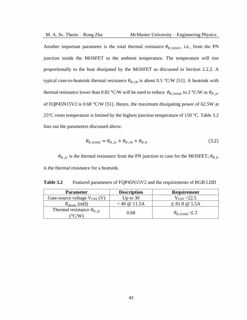
M. A. Sc. Thesis – Rong Zha McMaster University – Engineering Physics
42
Another important parameter is the total thermal resistance 𝜃𝑅_𝑡𝑜𝑡𝑎𝑙 , i.e., from the PN
junction inside the MOSFET to the ambient temperature. The temperature will rise
proportionally to the heat dissipated by the MOSFET as discussed in Section 2.2.2. A
typical case-to-heatsink thermal resistance 𝜃𝑅_𝑐ℎ is about 0.5 °C/W [51]. A heatsink with
thermal resistance lower than 0.82 °C/W will be used to reduce 𝜃𝑅_𝑡𝑜𝑡𝑎𝑙 to 2 °C/W as 𝜃𝑅_𝑗𝑐
of FQP45N15V2 is 0.68 °C/W [51]. Hence, the maximum dissipating power of 62.5W at
25°C room temperature is limited by the highest junction temperature of 150 °C. Table 3.2
lists out the parameters discussed above.
𝜃𝑅_𝑡𝑜𝑡𝑎𝑙 = 𝜃𝑅_𝑗𝑐 + 𝜃𝑅_𝑐ℎ + 𝜃𝑅_ℎ (3.2)
𝜃𝑅_𝑗𝑐 is the thermal resistance from the PN junction to case for the MOSFET; 𝜃𝑅_ℎ
is the thermal resistance for a heatsink.
Table 3.2 Featured parameters of FQP45N15V2 and the requirements of RGB LDD
Parameter Description Requirement
Gate-source voltage VGSS (V) Up to 30 VGSS >22.5
𝑅ⅆ𝑠𝑜𝑛 (mΩ) < 40 @ 11.5A ≤ 81.8 @ 5.5A
Thermal resistance 𝜃𝑅_𝑗𝑐
(°C/W) 0.68 𝜃𝑅_𝑡𝑜𝑡𝑎𝑙 ≤ 2

M. A. Sc. Thesis – Rong Zha McMaster University – Engineering Physics
43
Figure 3.4 Maximum SOA (red) of FQP45N15V2
Finally, the safe operating area (SOA) for the RGB LDD is acquired according to
Equation 3.2 as shown in Figure 3.4. The original DC line is calculated by thermal
resistance of 𝜃𝑅_𝑗𝑐, while the value of 𝜃𝑅_𝑡𝑜𝑡𝑎𝑙 is used for the calculation for our application.
It shows that FQP45N15V2 can withstand the continuous DC current with enough
redundancy. In the case of shunting all the LDs due to the OCP described in Section 3.3,
the power supply of +24 V will connect to the drain of the N MOSFET via the crowbar
circuits, which will increase the drain-source (VDS) voltage near 24 V. Combined with the
requirements in Table 3.2, allowable DC drain current of 2.3 A at VDS of 24 V, narrows
down the selection of the N MOSFET to FQP45N15V2.

M. A. Sc. Thesis – Rong Zha McMaster University – Engineering Physics
44
3.2.2 Selection of current sense resistors
As previously mentioned in Sections 2.2.2, 3.1 and 3.2.1, the voltage across the RMC is
less than 0.55 V. In this section, the RMC is chosen by analyzing it in detail.
The feedback loop of current regulation determines this voltage. In order to explain
the procedures of the regulation of the current, the circuits inside the iC-HTG are divided
into digital and analog circuits, which are indicated in the block diagrams of iC-HTG in
Figure 3.5 and the feedback loop path in Figure 2.8.
On the one hand, Figure 3.5 shows that the digital circuits accept the input data at
D1 and write these data into the registers inside two red rectangles at D2 and D3 in the
“RAM RESGISTER” block. Three digital stages are listed as below:
1. I2C interface at D1: in the case of setting the output current (𝐼), it receives two data
packages for D2 and D3 from the external controller via this interface.
2. The first data package at D2 for the D/A converter is a 10-bit binary value (N: 0-
1023 in decimal) stored in “REF (9:0)” at the addresses of 0x13 and 0x14.
3. The second data package at D3 is a 2-bit value for selecting the current gain (𝐶𝑔) in
“CURRENT CHANNEL”, stored at the address of 0x15. In Equation 3.3, this gain
factor is used to amplify the 𝑉𝑅𝑀𝐶 to 𝑉𝑀𝐶, which feeds back to the inverting input
of the operational amplifier in “LASER REGULATOR”. (The bit “MCVR”
depends on the positions of RMC in the current path as shown in Figure 3.3; “EACC”
selects the current or the optical power feedback.)
𝑉𝑀𝐶 = 𝐶𝑔𝑉𝑅𝑀𝐶 (3.3)

M. A. Sc. Thesis – Rong Zha McMaster University – Engineering Physics
45
Figure 3.5 Block diagram of iC-HTG with the controlling flow of the current regulation
Table 3.3 Gain setting of current channel for automatic current feedback control
CGAIN (1:0)
/EACC = 1, MCVR = 0 0x00 0x01 0x10 0x11
Cg 2 5 10 50
The output current is kept constant by the feedback loop between “LASER
REGULATOR” and “CURRENT CHANNEL” in the analog circuits. As seen in Figure
2.8, same current of 𝐼 flows through the LDs, N MOSFET and RMC due to the high input
resistance of MCH and VRN. In fact, this current value is determined by D2 and D3 if the
resistor value (𝑅𝑀𝐶) of RMC is already known.
𝐼 = 𝑉𝑅𝑀𝐶
𝑅𝑀𝐶 (3.4)

M. A. Sc. Thesis – Rong Zha McMaster University – Engineering Physics
46
Figure 3.5 also shows two analog stages A1 and A2 are used for this determination.
4. A1 connects the 10-bit D/A on the left to the non-inverting input of the operational
amplifier on the right. This D/A logarithmically converts the 10-bit digital value
into a voltage of 𝑉𝑠𝑒𝑡 in “LASER REGULATOR” block based on the following
Equation 3.5.
𝑉𝑠𝑒𝑡 = 𝑉𝑅𝐸𝐹0 (1 +∆𝑉𝑅𝐸𝐹(%)
100)
𝑁+1
, 𝑁 𝑓𝑟𝑜𝑚 0 𝑡𝑜1023 (3.5)
According to the datasheet [54], 𝑉𝑅𝐸𝐹0 is 0.1 V and ∆𝑉𝑅𝐸𝐹 (%) is 0.235 %, N is the
decimal value of “REF” register in the stage D2. 𝑉𝑠𝑒𝑡 is within the range of 0.1 to
1.1 V, calculated from the above equation.
0.1 < 𝑉𝑠𝑒𝑡 ≤ 1.1 (3.6)
5. A2 is the closed negative feedback loop, in which 𝑉𝑀𝐶 is forced to follow 𝑉𝑠𝑒𝑡 as in
Equation 3.7
𝑉𝑠𝑒𝑡 = 𝑉𝑀𝐶 (3.7)
Therefore, combined the equations from 3.3 to 3.7, 𝑉𝑅𝑀𝐶 and 𝐼 are decided by Inequation
3.8 and Equation 3.9. And 𝐶𝑔 is listed in Table 3.3.
0.002 <0.1
𝐶𝑔< 𝑉𝑅𝑀𝐶 ≤
1.1
𝐶𝑔≤ 0.55 (3.8)
𝐼 =𝑉𝑅𝐸𝐹0 (1 +
∆𝑉𝑅𝐸𝐹(%)100
)𝑁+1
𝐶𝑔𝑅𝑀𝐶=
(1.00235)𝑁+1
10𝐶𝑔𝑅𝑀𝐶 (3.9)

M. A. Sc. Thesis – Rong Zha McMaster University – Engineering Physics
47
Equation 3.9 reveals the current 𝐼 is controlled by the data N in the D2 stage and 𝐶𝑔 in the
D3 stages if 𝑅𝑀𝐶 is known.
Table 3.4 lists the 𝑅𝑀𝐶 values in different channels based on the calculation in
Inequation 3.10 and the specifications in Table 2.6. Two reasons to choose the higher value
of 𝑅𝑀𝐶 , limiting the current and improving the signal noise ratio.
𝑅𝑀𝐶 ≤5.5
𝐼𝑚𝑎𝑥 (3.10)
Table 3.4 𝑅𝑀𝐶𝑠 for RGB channels
Channel Red:
HL63283HD
Green:
NDG7475
Blue:
NDB7A75 DPSSL
𝐼𝑚𝑎𝑥 (A) 1.6 1.8 2.7 5.5
𝑅𝑀𝐶 (Ω) 0.3 0.3 0.2 0.1
3.3 Design of LD protection
In this section, a soft-start circuit generates a spike-free current during the power on stage.
Safe operation for the LDs is achieved by the internal features of iC-HTG as well as external
crowbar circuits. Also, a method of detecting open laser connection will be introduced.
Finally, a normally closed relay for ESD and transient protection, and a Schottky diode for
reverse protection are included in each channel.
3.3.1 Soft start and slow turn-on
Soft start is also known as slow start. In an early application note “protecting your laser
diode” from ILX Lightwave in 1996 [41], it was recommended that ramping up time of 100
ms for the output current is enough to prevent the turn-on transients.

M. A. Sc. Thesis – Rong Zha McMaster University – Engineering Physics
48
LDDs require a soft-start to protect the LDs. The FDA also mandates (CDRH US21
CFR 1040 10) a minimum turn-on delay of 2 s for personal safety [58]. This slow turn-on,
which can be easily implemented by a timer in hardware or a delay routine in software,
does not affect the current or voltage waveform. However, the confusion between these
two concepts causes some designers to use a longer soft-start. The designed LDD in this
research project will include both features, soft-start by hardware circuits in this Section
and a delay in the software.
One of the advantages of iC-HTG is the easy configuration for the soft-start.
Connecting a capacitor between pin “CI” and “CIL” enables this feature as shown in Figure
3.3 (a). Figure 3.6 shows a soft-start of the current, which can be represented by yellow
curve of 𝑉𝑅𝑀𝐶 according to Equation 3.4. As shown in the figure, current ramps up to 1.8
A without any overshoot with a 1 µF CI capacitor, which meets the requirement for the soft
start.
A minimum value of CI capacitor of 1000 𝑝𝐹 is recommended by the datasheet [54].
But the slope in the waveform of the current also depends on the other factors such as
MOSFET, PCB layout, LDs and the current range. In practical applications, the calculation
for the capacitance is impossible because the internal structure of iC-HTG is unknown. This
value can be obtained by trials on a prototype, as the purpose of the soft-start aims to supress
the turn-on transients not for the precisely timing of the ramp. Capacitors from hundreds
𝑛𝐹 to several 𝜇𝐹 are tested during the experiment. CI capacitor of 1 µF is used in the
application.

M. A. Sc. Thesis – Rong Zha McMaster University – Engineering Physics
49
Figure 3.6 Current ramping up to 1.8 A without overshoot; 𝑉𝑅𝑀𝐶 in yellow, 𝑉𝑅𝑁 in
purple, 𝑅𝑀𝐶 of 0.3 Ω, 𝐶𝐼 of 1µ𝐹
3.3.2 Overcurrent protection (OCP) by iC-HTG
As shown in Figure 3.6, the output current ramps up after the 𝑉𝑅𝑁 (the purple curve) linearly
rising above the turn-on threshold voltage of the N MOSFET. The current is forced to be
regulated by 𝑉𝑅𝑁 under the controlling flow from D1 to A2 as described in Section 3.2.2.
One straightforward way to implement the OCP is pulling down 𝑉𝑅𝑁 to shutdown the
current channel in the case of an over current event. Triggering this embedded OCP of iC-
HTG includes another three stages as shown in Figure 3.5.
6. A third 8-bit data package for P1 stage is received at D1. Then it is stored in “ILIM”
register at the address of 0x11. An 8-bit D/A linearly converts this value into the
voltage of 𝑉𝐼𝐿𝐼𝑀, which connects to the negative input terminal of the comparator.
7. During P2, “VCU” is internally connected between “LASER REGULATOR” and
“OVERCURRNT” blocks indicated by the dashed bi-arrow. As “EACC == 1” is
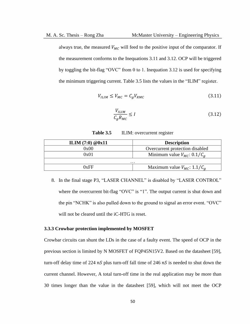
M. A. Sc. Thesis – Rong Zha McMaster University – Engineering Physics
50
always true, the measured 𝑉𝑀𝐶 will feed to the positive input of the comparator. If
the measurement conforms to the Inequations 3.11 and 3.12. OCP will be triggered
by toggling the bit-flag “OVC” from 0 to 1. Inequation 3.12 is used for specifying
the minimum triggering current. Table 3.5 lists the values in the “ILIM” register.
𝑉𝐼𝐿𝐼𝑀 ≤ 𝑉𝑀𝐶 = 𝐶𝑔𝑉𝑅𝑀𝐶 (3.11)
𝑉𝐼𝐿𝐼𝑀
𝐶𝑔𝑅𝑀𝐶≤ 𝐼 (3.12)
Table 3.5 ILIM: overcurrent register
ILIM (7:0) @0x11 Description
0x00 Overcurrent protection disabled
0x01 Minimum value 𝑉𝑀𝐶: 0.1 𝐶𝑔⁄
…
0xFF Maximum value 𝑉𝑀𝐶: 1.1 𝐶𝑔⁄
8. In the final stage P3, “LASER CHANNEL” is disabled by “LASER CONTROL”
where the overcurrent bit-flag “OVC” is “1”. The output current is shut down and
the pin “NCHK” is also pulled down to the ground to signal an error event. “OVC”
will not be cleared until the iC-HTG is reset.
3.3.3 Crowbar protection implemented by MOSFET
Crowbar circuits can shunt the LDs in the case of a faulty event. The speed of OCP in the
previous section is limited by N MOSFET of FQP45N15V2. Based on the datasheet [59],
turn-off delay time of 224 𝑛𝑆 plus turn-off fall time of 246 𝑛𝑆 is needed to shut down the
current channel. However, A total turn-off time in the real application may be more than
30 times longer than the value in the datasheet [59], which will not meet the OCP

M. A. Sc. Thesis – Rong Zha McMaster University – Engineering Physics
51
specifications in Table 2.6. If the channel of the LDD is saturated, the response time of the
OCP by the iC-HTG will be significantly increased. Crowbar circuits are designed to solve
these issues.
A conceptual diagram of the crowbar circuit is shown in Figure 3.7. A P MOSFET
is used to implement the shunting action in the crowbar circuits by shorting its source and
drain.
Figure 3.7 P MOSFET crowbar
Typically, crowbar circuits use a silicon-controlled rectifier (SCR). However, A
bench comparison between MOSFET and SCR for the crowbar protection circuits by
Analog Device company [60] shows that SCR has a slower shunting speed than MOSFET.
[61] demonstrates the successful shunting by a MOSFET can be applied to the LDs. In the
worst case, the MOSFET in the crowbar circuits shorts the LDs only for tens of
microseconds before the output channel can be totally shutdown by the iC-HTG as shown
in Section 5.3.3. The limitation in the selection of a fast MOSFET due to the SOA is relaxed.
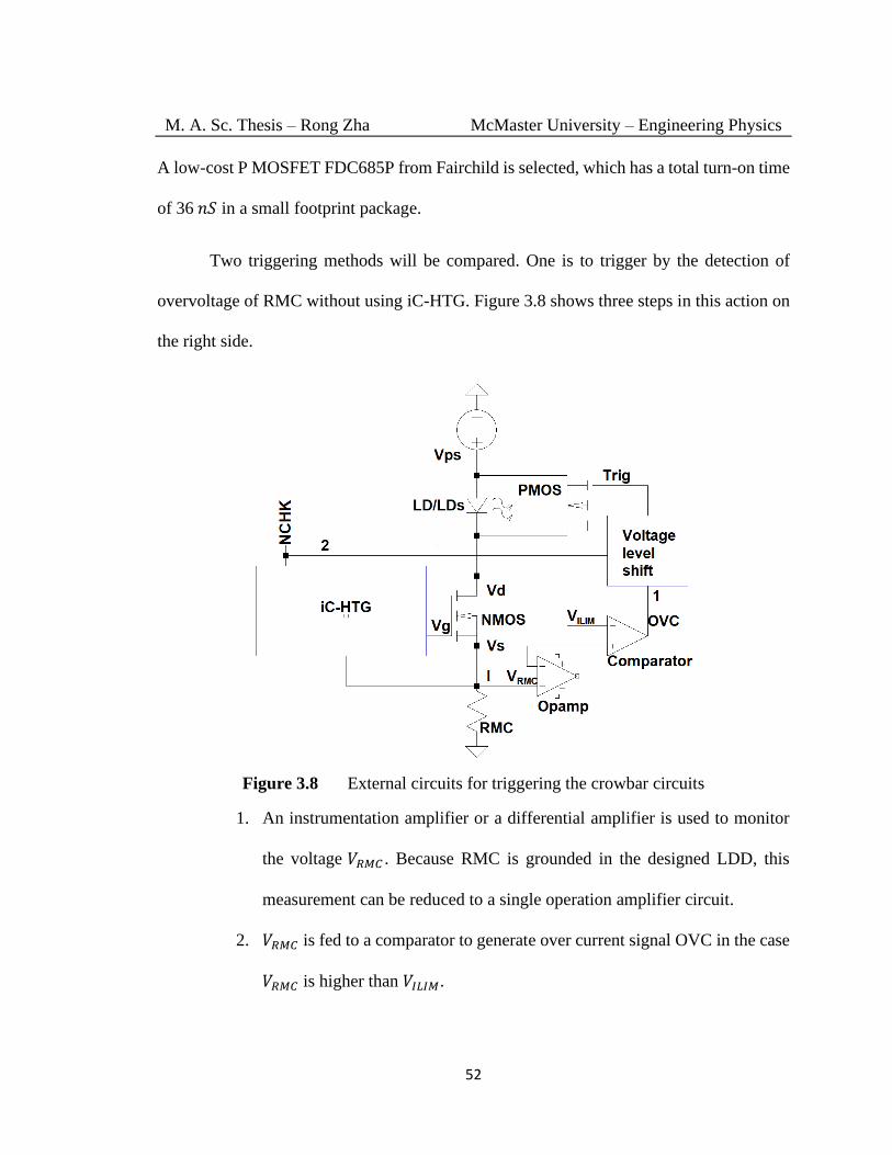
M. A. Sc. Thesis – Rong Zha McMaster University – Engineering Physics
52
A low-cost P MOSFET FDC685P from Fairchild is selected, which has a total turn-on time
of 36 𝑛𝑆 in a small footprint package.
Two triggering methods will be compared. One is to trigger by the detection of
overvoltage of RMC without using iC-HTG. Figure 3.8 shows three steps in this action on
the right side.
Figure 3.8 External circuits for triggering the crowbar circuits
1. An instrumentation amplifier or a differential amplifier is used to monitor
the voltage 𝑉𝑅𝑀𝐶 . Because RMC is grounded in the designed LDD, this
measurement can be reduced to a single operation amplifier circuit.
2. 𝑉𝑅𝑀𝐶 is fed to a comparator to generate over current signal OVC in the case
𝑉𝑅𝑀𝐶 is higher than 𝑉𝐼𝐿𝐼𝑀.

M. A. Sc. Thesis – Rong Zha McMaster University – Engineering Physics
53
3. A voltage level shift circuit is used to transform OVC to an effective
triggering voltage level to satisfy the turn-on requirement of 𝑉𝐺𝑆.
This external triggering method is independent of the iC-HTG at a cost of extra
components. Meanwhile, the triggering event also captured internally in the first two stages
of P1 and P2 in Section 3.3.2. Because the same monitoring and comparing functions have
been implemented internally by the iC-HTG. The problem is the flag-bit of OVC located
inside the address of 0x00 in “RAM REGISTERES”, which is not indicated by an output
pin. Although the value of OVC can be read by the I2C interface at D1. It will take longer
time to trigger the crowbar. As a result, the time for reading via I2C and the time for the
processing in the microcontroller make this choice impractical.
Figure 3.9 1.15 µs delay time from OVC event to NCHK output; NCHK in yellow
and 𝑉𝑅𝑀𝐶 in purple

M. A. Sc. Thesis – Rong Zha McMaster University – Engineering Physics
54
This issue can be solved by using the output pin “NCHK”. “NCHK” is the
abbreviation for “check output, active low”. This open drain output will be actively
grounded in the case of an OVC event. Although no information about the delay time from
the OVC event to “NCHK” output. An experiment was carried out to estimate the duration
of this delay. As shown in Figure 3.9, from OVC event to NCHK output, a delay of 1.15
µs is measured by the oscilloscope. In the measurement, two 7 Ω aluminum alloy resistors
are connected in series as dummy loads. Two probes are hooked up to 𝑉𝑅𝑀𝐶 and “NCHK”
respectively. An overcurrent event is triggered by shorting one dummy load. The result
shows the duration of the delay is acceptable since the requirement of OCP is within 4 µs.
Solution 2 as shown in Figure 3.8 converts “NCHK” from iC-HTG into a crowbar
triggering signal in an allowable delay since the shunting action of P MOSFET FDC685AP
can be completed in less than 1 µs after the triggering. The voltage level shift circuits only
require 4 small SMT components, with a PCB size of less than 1 cm2.
Figure 3.10 shows a voltage level shifter with a detailed schematic and PCB
dimensions. The voltage level shift circuit is also called the voltage level shifter or
translator. It is used in the systems where two sections operate from different voltage levels.
On-off of P MOSFET of Q2 is controlled by its gate-source voltage. The source of Q2 is
connected to 𝑉𝑝𝑠 of +24 V as seen in Figure 3.8 and is labeled “LD_AN” in Figure 3.10.
In order to fully turn off the P MOSFET, the gate voltage of Q2 needs to be +24V. A voltage
level shifter from “NCHK” to the gate of Q2 is needed since the highest voltage of “NCHK”
is 5.5 V [54]. Figure 3.10 shows when “NCHK” is an active-low signal, the gate of Q2
will be grounded to turn on the Q2. If “NCHK” is pulled up to VDD when there is no faulty

M. A. Sc. Thesis – Rong Zha McMaster University – Engineering Physics
55
event, the gate voltage will be same as the source voltage to turn off the Q2. Table 3.6 lists
the logic relations for this triggering action.
Table 3.6 “NCHK” triggering P MOSFET Q2 with a voltage level shifter
NCHK Q3 𝑽𝒈𝒔 of Q2 (V) Q2
LOW Q3A: ON; Q3B; OFF -24 ON
HIGH Q3A: OFF; Q3B; ON 0 OFF
Figure 3.10 Schematic and PCB of a voltage level shifter
Currently, there is no standard value for the delay time of OCP. In 2018, [62]
specifies OCP delay time of 125 µs. Meerstetter Engineering GmbH indicates the delay of
OCP within 6-8 µs [63] in the manual. Delay of OCP in less than 4 µs can effectively
protect the LDs [64]. We therefore target this value in our design.
3.3.4 Overvoltage protection
The crowbar circuits can also be used for overvoltage protection (OVP). The triggering
signal from 𝑉𝑅𝑀𝐶 is changed to the voltage across the LDs (𝑉𝐿𝐷𝑠) in the first step as shown

M. A. Sc. Thesis – Rong Zha McMaster University – Engineering Physics
56
in Figure 3.8. An instrumentation amplifier or a differential amplifier is used to monitor the
voltage 𝑉𝐿𝐷𝑠. The other two steps remain unchanged with the addition of the following two:
1. 𝑉𝐿𝐷𝑠 is much higher than 𝑉𝑅𝑀𝐶. Hence, the measurement of voltage may need an
attenuator. Instability of the amplifier when the gain is less than one must be taken
care of.
2. The comparator needs latching function in the output. Because the shorting of P
MOSFET changes 𝑉𝑜𝑢𝑡 , which will cause the comparator output 𝑉𝑐𝑜𝑚 to be toggled
as shown Figure 3.12.
The conceptual circuit simulations below suggest this OVP can be effective with the
crowbar circuits. It is convenient to use voltage divider to simulate OVP in Figures 3.11
and 3.13, i.e., R1 representing for LDs and R7 for the N MOSFET plus the RMC. As shown
in Figures 3.12 and 3.14, LDs, N MOSFET and RMC are connected in series and the
shunting of the crowbar circuits will reduce the voltage of 𝑉𝐿𝐷𝑠.
𝑉𝐿𝐷𝑠 = 𝑉2 − 𝑉𝑡𝑒𝑠𝑡 (3.13)

M. A. Sc. Thesis – Rong Zha McMaster University – Engineering Physics
57
Figure 3.11 OVP by MOSFET crowbar circuits, comparator without latching function
Figure 3.12 Simulation results for OVP in Figure 3.11
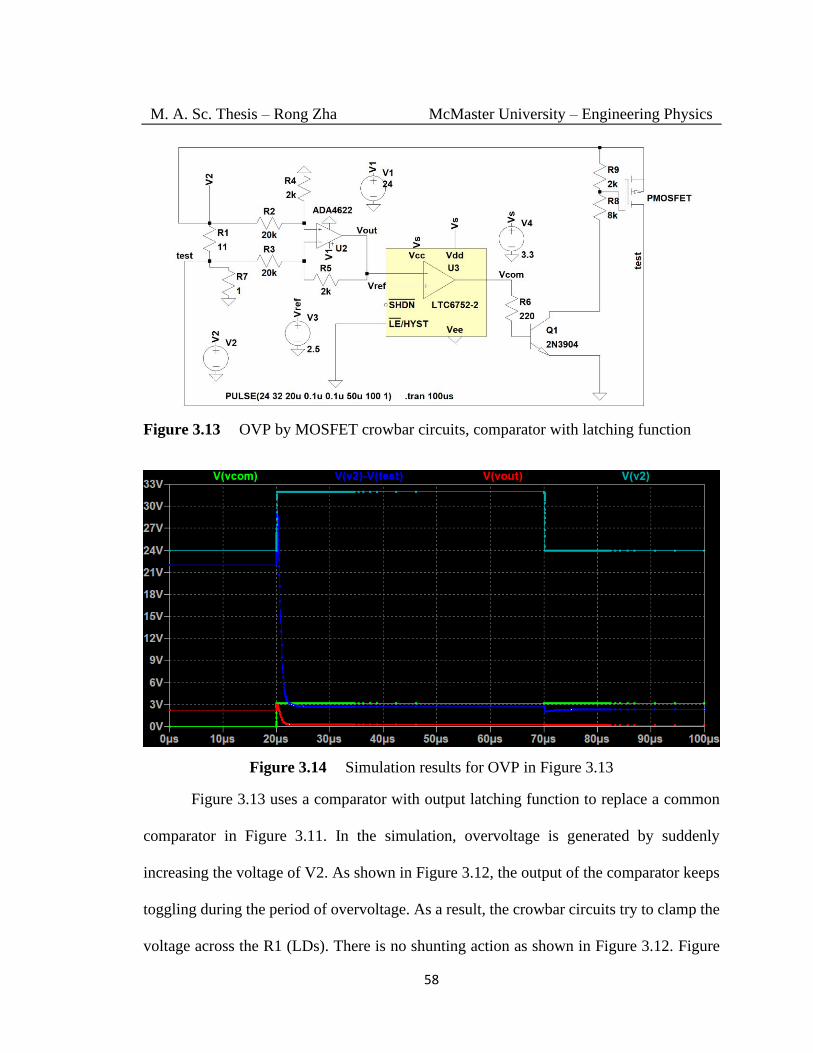
M. A. Sc. Thesis – Rong Zha McMaster University – Engineering Physics
58
Figure 3.13 OVP by MOSFET crowbar circuits, comparator with latching function
Figure 3.14 Simulation results for OVP in Figure 3.13
Figure 3.13 uses a comparator with output latching function to replace a common
comparator in Figure 3.11. In the simulation, overvoltage is generated by suddenly
increasing the voltage of V2. As shown in Figure 3.12, the output of the comparator keeps
toggling during the period of overvoltage. As a result, the crowbar circuits try to clamp the
voltage across the R1 (LDs). There is no shunting action as shown in Figure 3.12. Figure

M. A. Sc. Thesis – Rong Zha McMaster University – Engineering Physics
59
3.14 shows an effective shunting action of the crowbar circuits. Comparator output is
latched to high even if the over-voltage event disappears. Therefore, the output latching
function of the comparator guarantees the shunting action of the crowbar circuits as long
as the OVP is triggered.
Unfortunately, the cost for the crowbar circuits is too high. The estimated cost for
eight channels is eighty dollars. Besides the cost, the size and the complexity of the circuit
will be another problem. At least one hundred components are needed for eight channels
as well as different power rails for the amplifier and the comparator. Therefore, it is optimal
to find an alternative method to solve these issues.
OVP protects LDs against overvoltage. Further analysis for the triggering of over-
voltage event can help to find an alternative method.
Two scenarios for this event, with or without the occurrence of the overcurrent
respectively, are described as below:
1. With overcurrent: overcurrent happens simultaneously with overvoltage according
to the V-I curve of the LD.
2. Without overcurrent:
1) Overvoltage is generated by the open connection of the leads from the LDs
as shown in Figure 3.15. Disconnection occurring at any location inside the
LDs will cause the measured voltage across the LDs to be 𝑉𝐿𝐷𝑠𝑂𝑝𝑒𝑛 .
Because no current flows through N MOSFET and RMC, 𝑉𝐷 at the drain of
the N MOSFET will be pulled down to ground, which drives 𝑉𝐿𝐷𝑠𝑂𝑝𝑒𝑛 to

M. A. Sc. Thesis – Rong Zha McMaster University – Engineering Physics
60
the power supply in equation 3.14. 𝑉𝐿𝐷𝑠 is the voltage across the LDs in
normal connection.
𝑉𝑝𝑠 = 𝑉𝐿𝐷𝑠 + 𝑉𝐷 = 𝑉𝐿𝐷𝑠𝑂𝑝𝑒𝑛 (3.14)
Figure 3.15 Overvoltage due to open connection of LDs
2) Overvoltage is generated by saturation in the current feedback loop. The
voltage across the LDs is higher than the compliance voltage of the LDD
channel.
The first scenario was already solved by OCP and the crowbar circuits in Section
3.3.2 and 3.3.3. Both situations in the second scenario will affect the feedback loop for the
current regulation inside the iC-HTG. The negative closed feedback loop of the current
regulation, which was described as A1 and A2 in Section 3.2.2, is disrupted by the open
connection of the LDs in the first situation or become unstable in the second situation. Loop
stability in Figure 3.5 is achieved by minimizing the difference (∆) between the inputs of
the operational amplifier to zero as listed in Table 3.7.

M. A. Sc. Thesis – Rong Zha McMaster University – Engineering Physics
61
Table 3.7 Current regulation by a negative closed feedback loop
∆= 𝑽𝒔𝒆𝒕 − 𝑽𝑴𝑪 𝑽𝑹𝑵 𝑰 |∆| > 0 ↗ ↗ ↙
< 0 ↙ ↙ ↙
= 0 stable stable 0
If the current is cut off by the open circuit or less than the setting value, Equation
3.7 becomes Inequation 3.15. Consequently, |∆| cannot decrease to zero at the input of the
operation amplifier since the current can not increase to the setting value, which will drive
𝑉𝑅𝑁 to keep increasing, until to its maximum output (𝑉𝐵𝐿 − 1.5) V. This is another reason
why the parameter 𝑉𝐺𝑆𝑆 in Table 3.2 is chosen.
𝑉𝑠𝑒𝑡 > 𝑉𝑀𝐶 (3.15)
In the first situation, a combination of 𝑉𝑝𝑠 (𝑉𝑝𝑠 is connected to 𝑉𝐵𝐿) and 𝑉𝐷 in Figure
3.15 is used to implement the detection of the faulty open connection of the LDs due to the
bad soldering or mechanical wear-out in Table 3.8.
Table 3.8 Channel status detected by 𝑉𝑅𝑁 and 𝑉𝐷
𝑰 𝑽𝑹𝑵 𝑽𝑫 𝑽𝒑𝒔 Status of channel
0 0 0 0 Power off
0 0 𝑉𝑝𝑠 > 0 Normally disabled
0 0 0 > 𝟎
Open circuit in laser
connection when the
channel is disabled
𝐼 𝑉𝐺𝑆𝑡ℎ < 𝑉𝑅𝑁 𝐼𝑅𝑀𝐶 < 𝑉𝐷 < 𝑉𝑝𝑠 > 0 Normally enabled
0 𝑉𝑅𝑁 > 0 and keeps
increasing to (𝑉𝑝𝑠 − 1.5) 0 > 𝟎
Open laser connection
when the channel is
enabled
< 𝐼 𝑉𝑅𝑁 > 𝑉𝐺𝑆𝑡ℎ and keeps
increasing to (𝑉𝑝𝑠 − 1.5) 𝐼𝑅𝑀𝐶 < 𝑉𝐷 < 𝑉𝑝𝑠 > 0
Abnormal saturation in
current feedback loop
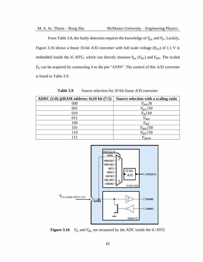
M. A. Sc. Thesis – Rong Zha McMaster University – Engineering Physics
62
From Table 3.8, the faulty detection requires the knowledge of 𝑉𝑝𝑠 and 𝑉𝐷. Luckily,
Figure 3.16 shows a linear 10-bit A/D converter with full scale voltage (𝑉𝐹𝑆) of 1.1 V is
embedded inside the iC-HTG, which can directly measure 𝑉𝑝𝑠 (𝑉𝐵𝐿) and 𝑉𝑅𝑁. The scaled
𝑉𝐷 can be acquired by connecting it to the pin “ANIN”. The control of this A/D converter
is listed in Table 3.9.
Table 3.9 Source selection for 10-bit linear A/D converter
ADDC (2:0) @RAM address: 0x10 bit (7:5) Source selection with a scaling ratio
000 𝑉𝐷𝐷/8
001 𝑉𝐵𝐿/30
010 𝑉𝐵/30
011 𝑉𝑀𝐷
100 𝑉𝑀𝐶
101 𝑉𝑅𝑁/30
110 𝑉𝑅𝑃/30
111 𝑉𝐴𝑁𝐼𝑁
Figure 3.16 𝑉𝐷 and 𝑉𝐵𝐿 are measured by the ADC inside the iC-HTG

M. A. Sc. Thesis – Rong Zha McMaster University – Engineering Physics
63
𝑉𝑝𝑠 = 𝑉𝐵𝐿 = 30𝑁𝐴𝐷𝐶
1024𝑉𝐹𝑆 =
33
1024𝑁𝐴𝐷𝐶 (3.16)
𝑉𝐷 = 𝑅𝑆𝐶
𝑁𝐴𝐷𝐶
1024𝑉𝐹𝑆 ; 𝑅𝑆𝐶 =
𝑉𝐷
𝑉𝐴𝑁𝐼𝑁>
24
1.1 = 21.8 (3. 17)
𝑅𝑆𝐶 greater than 21.8 is used to scale down 𝑉𝐷 within the voltage range of “ANIN”,
which can be implemented by a voltage divider circuit. The value of 𝑅𝑆𝐶 is similar as the
scaling ratio for 𝑉𝐵𝐿 because the maximum 𝑉𝐷 is equal to 𝑉𝐵𝐿. 31.93 is selected for 𝑅𝑆𝐶 by
using standard 15k and 464k resistors with 1% precision.
Another way to solve the issue of the open laser connection is by monitoring 𝑉𝑀𝐶
and 𝑉𝑅𝑁 . It seems more convenient to use this method because 𝑉𝑀𝐶 is readily available
from A/D converter as shown in Figure 3.16. Table 3.10 is based on Table 3.7 and
Inequation 3.15, which can be used for this faulty detection.
Table 3.10 Channel status detected by 𝑉𝑅𝑁 and 𝑉𝑀𝐶
𝑽𝑹𝑵 𝑽𝑴𝑪 Status of channel
0 0 0 Power off or normally
disabled
𝐼 𝑉𝐺𝑆𝑡ℎ < 𝑉𝑅𝑁 𝐼𝑅𝑀𝐶𝐶𝑔 = 𝑉𝑀𝐶 Normally enabled
0 𝑉𝑅𝑁 > 𝑉𝐺𝑆𝑡ℎ and keeps increasing
to (𝑉𝐵𝐿 − 1.5) 0
Open laser connection
when the channel is
enabled
0 0 < 𝑉𝑅𝑁 < 𝑉𝐺𝑆𝑡ℎ 0 Unknown
< 𝐼 𝑉𝑅𝑁 > 𝑉𝐺𝑆𝑡ℎ and keeps increasing
to (𝑉𝐵𝐿 − 1.5) 𝐼𝑅𝑀𝐶𝐶𝑔 < 𝑉𝑀𝐶
Abnormal saturation
in current feedback
loop
The most important advantage of using the method shown in Table 3.8 is that the
open circuit faulty condition can be detected before the output channel is enabled. It also

M. A. Sc. Thesis – Rong Zha McMaster University – Engineering Physics
64
has one more specific channel status of “normally disabled”. On the other side, the
detection speed for the open connection shown in table 3.10 is slower due to the turn-on
delay of N MOSFET because there is an unknown status for the channel. When 𝑉𝑅𝑁 is
lower than 𝑉𝐺𝑆𝑡ℎ, the MOSFET will be off without current flowing into RMC. Moreover,
the soft-start will make it even worse. Therefore, the method of the detection of open laser
connection shown in Table 3.8 will be used.
In the second situation, abnormal saturation of the current feedback loop is also
included in Table 3.8 and 3.10. The current can not ramp up to a setting value greater than
𝐼𝑠𝑎𝑡 due to exceeding the maximum number 𝑛𝑚𝑎𝑥 of the LDs in the channel. From
Equation 3.3, the maximum output current 𝐼𝑠𝑎𝑡can be calculated as:
𝐼 = 𝑉𝑝𝑠 − 𝑉𝐿𝐷𝑠
𝑅𝑁𝑀𝑂𝑆 + 𝑅𝑀𝐶 ≤
𝑉𝑝𝑠 − 𝑛𝑚𝑎𝑥𝑉𝐿𝐷
𝑅ⅆ𝑠𝑜𝑛 + 𝑅𝑀𝐶 = 𝐼𝑠𝑎𝑡 (3.18)
The current feedback loop forces 𝑉𝑅𝑁 to rise in order to increase the current in the
channel. But the increase of the current will raise the voltage 𝑉𝐿𝐷𝑠 across the LDs. In return,
the voltage across the MOSFET will fall as 𝑅𝑁𝑀𝑂𝑆 can decrease as a variable resistor in
saturation region, which eventually turns the MOSFET into the linear region in Equation
3.18. 𝑅ⅆ𝑠𝑜𝑛 , the minimum 𝑅𝑁𝑀𝑂𝑆 in the linear region, cannot be reduced any further. This
causes a closed negative feedback loop cannot reach a stable state. In other words, If the
setting current is higher than 𝐼𝑠𝑎𝑡, the current feedback loop is saturated, which drives 𝑉𝑅𝑁
to the maximum value. The negative feedback input on the inverting input of the
operational amplifier is always less than the non-inverting input of the operational amplifier
as shown in Inequation 3.15.

M. A. Sc. Thesis – Rong Zha McMaster University – Engineering Physics
65
Saturation does not refer to the saturation region of the MOSFET. In fact, it happens
in the linear region of MOSFET. “Abnormal” means the saturation status in the current
feedback should not be allowed for the LDDs. The MOSFET in linear region with
maximum 𝑉𝑅𝑁 makes this status very dangerous for the LDs in series connection. If the
resistance of LDs was suddenly reduced, for example shorting one LD causing a decrease
of voltage of 𝛥𝑉ⅆ𝑠 across the LDs. Consequently, the increase of voltage of 𝛥𝑉ⅆ𝑠 will
appear on the MOSFET. The current change in the channel is calculated in Equation 3.19.
𝛥𝐼ⅆ𝑠_𝑙𝑖𝑛𝑒𝑎𝑟 = 𝛥𝑉ⅆ𝑠
𝑅ⅆ𝑠𝑜𝑛 (3.19)
This equation also explains why this region is called as “linear region”. The LDs in
series connection will be overdriven until the feedback loop can reduce the current in this
error event. Although brief, this overdrive is generally enough to damage the LDs in this
channel.
For this reason, a program in the firmware for detecting the faulty open laser
connection and the saturation in the current feedback loop is developed. It will be discussed
in Section 4.5.
3.3.5 Shorting relay for ESD protection
A shorting relay is used for ESD protection when the system is power off. This device can
be omitted for the blue and green channels, because the green and blue LDs from Nichia
come with built-in protection circuits.
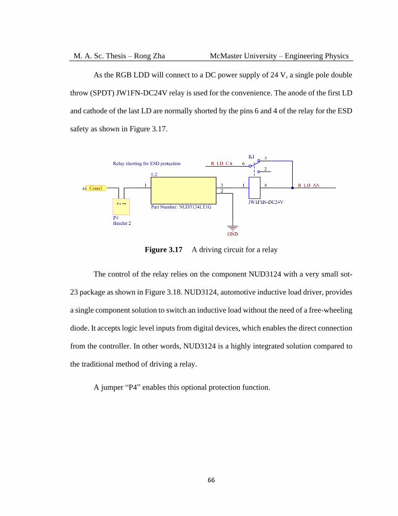
M. A. Sc. Thesis – Rong Zha McMaster University – Engineering Physics
66
As the RGB LDD will connect to a DC power supply of 24 V, a single pole double
throw (SPDT) JW1FN-DC24V relay is used for the convenience. The anode of the first LD
and cathode of the last LD are normally shorted by the pins 6 and 4 of the relay for the ESD
safety as shown in Figure 3.17.
Figure 3.17 A driving circuit for a relay
The control of the relay relies on the component NUD3124 with a very small sot-
23 package as shown in Figure 3.18. NUD3124, automotive inductive load driver, provides
a single component solution to switch an inductive load without the need of a free-wheeling
diode. It accepts logic level inputs from digital devices, which enables the direct connection
from the controller. In other words, NUD3124 is a highly integrated solution compared to
the traditional method of driving a relay.
A jumper “P4” enables this optional protection function.

M. A. Sc. Thesis – Rong Zha McMaster University – Engineering Physics
67
Figure 3.18 PCB size for the circuits of NUD3124
3.3.6 Reverse protection
Figure 3.19 shows reverse current was generated by an OEM switch mode LDD, when
there was a sudden disruption of power supply. In the measurement, two 7Ω dummy loads
were connected in series between the output terminals of the LDD. The lower side (farther
away form terminal of +24 V) one was measured by an oscilloscope. In Figure 3.19, the
yellow and purple curves are the recorded voltage waveforms during the power-off period.
Maximum reverse differential voltage of 3.5 V, i.e., 700 𝑚𝐴, was captured, which exceeded
the maximum allowable range for all the LDs. This problem was solved by paralleling a
reversed Schottky diode across the output terminals.

M. A. Sc. Thesis – Rong Zha McMaster University – Engineering Physics
68
Figure 3.19 Reverse voltage from an OEM switch mode LDD
Although reverse voltage is not detected in our design, Figure 3.20 shows that a
reversely connected Schottky diode is reserved in RGB LDD for better protection. This is
also a common method to protect against ESD from reverse direction.
Figure 3.20 Reverse protection by a reversed Schottky diode

M. A. Sc. Thesis – Rong Zha McMaster University – Engineering Physics
69
3.4 Communication interfaces
A communication interface to the RGB LDD is necessary for the users to implement the
functions listed in Table 1.2, Section 1.2.2. In this case, the RGB LDD can be controlled
by the main circuits of the projector. This first communication interface is intended for this
purpose, which help the users to regard RGB LDD as a black box. Inside of the RGB LDD,
another communication interface to link all the channels will be built by the designer.
Figure 3.21 shows that the communication interface of COMM1 is a UART, a
common communication interface available from any micro-controller. It can receive
different commands from the projector listed in Table 1.2 and also can send out the values
from the RAM registers, which are located inside the iC-HTGs. These values can be used
to monitor the status of the LDs.
Figure 3.21 A block diagram for the communication interfaces in the RGB LDD
In order to transfer the commands from the projector to a specified channel or
request the status information from the RAM registers in a designated channel, an internal

M. A. Sc. Thesis – Rong Zha McMaster University – Engineering Physics
70
communication interface of COMM2 is required that can identify different addresses from
different channels.
IC-HTG can support Serial Peripheral Interface (SPI) [65] and Inter-Integrated
Circuit (I2C) [66]. The reason for choosing I2C to link all the channels to the micro-
controller (MCU) is to minimize the component counts in the design. SPI will require more
pins from the “master” since each SPI “slave” is selected by one “slave select” (𝑆𝑆̅̅ ̅) signal
from the “master”. In our case, 8 pins from the MCU will be used as 𝑆𝑆1̅̅ ̅̅ ̅-𝑆𝑆8̅̅ ̅̅ ̅ signals. A
common solution to this issue is to connect a 3-line to 8-line decoder to the MCU.
I2C can reduce this hardware cost since it only needs two signals from the MCU as
shown in Figure 3.21. Figure 3.22 shows the encoding of the LDD channel by configurating
three pins from iC-HTG as listed in Table 3.11. I2C bus protocol uses high 7 bits as the
address and the lowest bit for the reading and writing actions as shown in Table 3.12.
Table 3.11 Configuration of I2C address for eight LDD channels
Pin LDD0 LDD1 LDD2 LDD3 LDD4 LDD5 LDD6 LDD7
4: ID 0 0 0 0 1 1 1 1
3: A1 0 0 1 1 0 0 1 1
6: A0 0 1 0 1 0 1 0 1
Table 3.12 I2C address for eight LDD channels
Action Bit7-4 (prefixed by manufacturer) Bit3 Bit2 Bit1 Bit0
Write 1 0 1 0 ID A1 A0 0
Read 1 0 1 0 ID A1 A0 1
To access an LDD channel, reading and writing commands derived from Table 3.12
are listed in Table 3.13. Only high 7-bit without lowest RW bit is used as the address in the
compliers.

M. A. Sc. Thesis – Rong Zha McMaster University – Engineering Physics
71
Table 3.13 I2C commands of reading and writing for the LDD channels
Address LDD0 LDD1 LDD2 LDD3 LDD4 LDD5 LDD6 LDD7
Write 0𝑥𝐴0 0𝑥𝐴2 0𝑥𝐴4 0𝑥𝐴6 0𝑥𝐴8 0𝑥𝐴𝐴 0𝑥𝐴𝐶 0𝑥𝐴𝐸
Read 0𝑥𝐴1 0𝑥𝐴3 0𝑥𝐴5 0𝑥𝐴7 0𝑥𝐴9 0𝑥𝐴𝐵 0𝑥𝐴𝐷 0𝑥𝐴𝐹
7-bit Address 0𝑥50 0𝑥51 0𝑥52 0𝑥53 0𝑥54 0𝑥55 0𝑥56 0𝑥57
The “master” MCU use these commands to control and monitor the LDD channels
via an SDA line. Because the address information of each channel is already included in
these commands, the “slave selection” signal is not needed in the I2C protocol. Two 1 kΩ
pull-up resistors are needed for SDA and SCLK because of the open-drain structure.
Figure 3.22 I2C for eight LDD channels
The implementation of the protocols for UART and I2C in firmware will be
discussed in chapter 4.
If the developers of the laser projector do not see RGB LDD as a black box, it is
possible for them to directly control the LDD channels without the MCU in between if

M. A. Sc. Thesis – Rong Zha McMaster University – Engineering Physics
72
there is an I2C interface in projector main circuits. However, they will need to modify the
software in the projector side, which is impossible in our application.
3.5 DC-DC module
A DC-DC module can boost the efficiency in the output channel. Off-the-shelf i6A Series
DC/DC power modules with 9-53V input and 20A output from TDK Lambda are used.
These modules with small form factors as shown in Figure 3.23 can satisfy requirement of
the compactness in the application.
(a) (b)
Figure 3.23 (a) Top and (b) bottom of i6A240 from TDK Lambda
Because it is easy to bypass a plug-in DC-DC module on the PCB, four DC-DC
footprints are included in the designed PCB for the maximum flexibility to drive different
configurations of the LDs in the future. To bypass an DC-DC module from the PCB, do
not plug in this module. Instead, flying a wire from the DC-DC’s positive input hole (pad)
to its positive output PCB hole (pad), i.e., shorting the two soldering points, can solve the
problem. A 10 kΩ potentiometer is used to adjust the output voltage in Figure 3.24. And a
capacitor (EEH-ZA1H101P) with low ESR, less than 100 mΩ under 100 kHz, is
recommended to connect to the input of the module by TDK Lambda [67].

M. A. Sc. Thesis – Rong Zha McMaster University – Engineering Physics
73
Figure 3.24 DC-DC modules

M. A. Sc. Thesis – Rong Zha McMaster University – Engineering Physics
74
3.5 Summary
In this chapter, a bottom-up approach has been used to describe the functions of the
hardware circuits according to the specifications in Table 2.6. A schematic for an LDD
channel for red LDs has been drawn in Figure 3.25. The block diagram for eight LDD
channels in a top-level sheet from the hierarchical schematics has been shown in Figure
3.26. The idea behind this design is to exploit the embedded features of iC-HTG as fully as
possible.
A configuration of current sink has been selected for a higher compliance voltage.
N MOSFETs and current sense resistors have been chosen by the calculation of the
performance in the current regulation.
Three core components inside the iC-HTG with their own controlling registers have
been used to protect for the LDs. A 10-bit logarithmic D/A converter has been used to set
the value of driving current in the LDD channel. OCP by iC-HTG and the crowbar circuits
have been configurated by an 8-bit linear D/A converter. Overvoltage and the open laser
detection have been implemented by another 10-bit linear A/D converter. Meanwhile, a
capacitor for soft-start, a Schottky diode for reverse protection and an ESD shorting relay
have been included in each LDD channel. Finally, external UART interface and internal
I2C interface have been introduced as well as an off-the-shelf i6A DC-DC plug-in module.
Between eight LDD channels and the UART, an MCU receives commands from
the projector and controls the LDD channels via I2C bus. These functions are implemented
in the firmware, which will be discussed in Chapter 4.

M. A. Sc. Thesis – Rong Zha McMaster University – Engineering Physics
75
Figure 3.25 Red LDD channel

M. A. Sc. Thesis – Rong Zha McMaster University – Engineering Physics
76
Figure 3.26 Top level diagram of RGB LDD
M. A. Sc. Thesis – Rong Zha McMaster University – Engineering Physics
77
Chapter 4
Firmware Design for the RGB LDD
Software, in particular “provides the low-level control for the device’s specific hardware”
[68], names as firmware in the embedded system which is distinguished from the
application software in the host computer. In this chapter, only the firmware for the MCU
will be designed. While the software in the host computer for UART is chosen from
available ones.
This chapter is organized in a top-down approach. In Section 4.1, an overall
flowchart for the firmware is drawn by decomposing the functions into the subroutines. A
main program will sequence through them in turn. Four functions are performed in the
MCU firmware: UART communication in Section 4.2, I2C communication between MUC
and the LDD channels in Section 4.3, decoding from UART to I2C in Section 4.4, and the
detection of faulty status of the LDs in Section4.5, which is the protection feature
implemented by firmware according to Chapter 3. In Section 4.6, a brief introduction of
the selected UART tool in the host is presented. The chapter ends with a summary.
4.1 Overall design
In this research project, we retrofitted a lamp-based projectors into an RGB laser projector.
Hence, the communication protocols for controlling the driver of light source in the
projector is not available to us. Different manufacturers have different motherboards for
their products. Therefore, in order to implement a general communication function

M. A. Sc. Thesis – Rong Zha McMaster University – Engineering Physics
78
discussed in Section 3.4, a software program for controlling the RGB LDD in the host
computer to mimic the general behavior of a projector is needed as shown in Figure 4.1.
Commands and requests from the software in the host computer to the RGB LDD will be
conducted via the lower level firmware resided in the MCU, which will link the eight LDD
channels with the host computer.
Figure 4.1 Software in the host computer and firmware in the MCU
There are two objectives to be fulfilled in the communications as shown in Figure
4.1.
1. One is between the host computer and the MCU by the UART.
2. The other is for delivering the commands and requests to the LDD channels
and receiving the status information from the LDD channels.
Two other objectives need to be achieved in order to protect the LDs in the error
events.
3. Disable the channel if open laser connection is detected.
4. Avoid the saturation of the LDD channel.
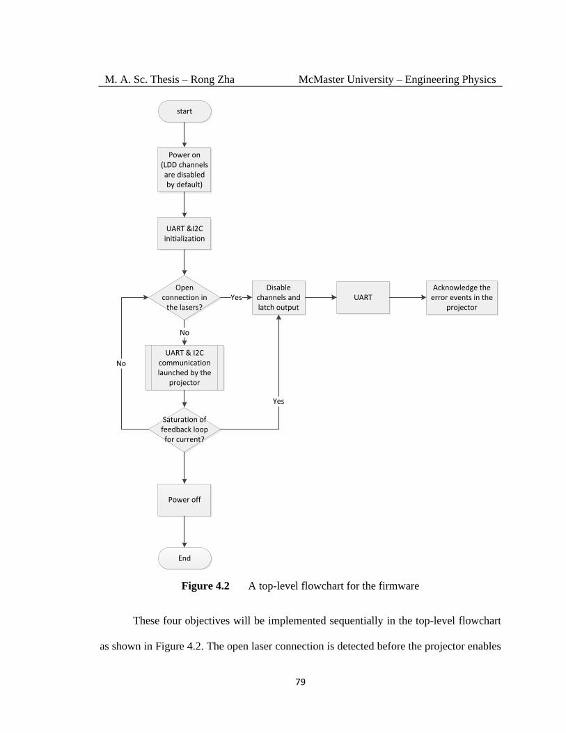
M. A. Sc. Thesis – Rong Zha McMaster University – Engineering Physics
79
start
Power on(LDD channels are disabled by default)
UART &I2C initialization
Open connection in
the lasers?
Disable channels and latch output
Yes UARTAcknowledge the
error events in the projector
UART & I2Ccommunication launched by the
projector
No
Saturation of feedback loop for current?
Yes
No
Power off
End
Figure 4.2 A top-level flowchart for the firmware
These four objectives will be implemented sequentially in the top-level flowchart
as shown in Figure 4.2. The open laser connection is detected before the projector enables

M. A. Sc. Thesis – Rong Zha McMaster University – Engineering Physics
80
the laser channel. This monitoring continues after the laser channels are enabled in the sub
flowchart of “UART & I2C communication launched by the projector”. Detected saturation
in the current feedback loop disables the channels, which will be acknowledged by the
projector as well as the error event of the open laser connection.
MCU UARTReceiving an instruction?
Command or request?
Echo Command
Yes, RXD of MCU
Echo+data8
Request
Start
Execute command
via I2C
UART transmitting
buffer
TXD of MCU
UARTreceiving
buffer
No
Host computer
Stage2Stage2
Stage3Stage3
Waiting for the
insturctions
Stage1Stage1
Execute request via
I2C
Figure 4.3 Flowchart of UART
The sub flowchart of “UART & I2C communication launched by the projector” is
unfolded in Figure 4.3. In this figure, three stages for the communication are designed to

M. A. Sc. Thesis – Rong Zha McMaster University – Engineering Physics
81
fulfill the objectives of communication accordingly which are indicated by the dashed line
and circle.
1. The host computer mimics the projector to control the RGB LDD by sending
commands and monitors the LDs by requesting the status information from the
RAM register inside the iC-HTGs.
2. UART of the MCU receives instructions from the host computer via pin RXD.
These instructions can be the commands, or the requests made by the “projector”.
Commands are used to control the iC-HTGs including enabling and disabling the
LDDs, adjusting the current, etc. While the requests are sent to the RGB LDD for
acquiring the status information from the requested RAM addresses. The
commands will be echoed back to the host computer via pin TXD for verification
along with the requested RAM data. Commercial lamp drivers also use the same
echoing method. The purpose of designing it in the RGB LDD is to help the
projector designers regard the light source module as a black box. Namely, it is not
necessary for them to modify the firmware in the projector while the lamp can be
replaced by the RGB LDs as long as the original formats of the commands and the
requests are also adopted in the RGB LDD. This stage will be discussed in Section
4.2.
3. Either the commands or the requests in I2C are needed to be written to or read from
the RAM registers inside the iC-HTGs. This stage is mainly about the I2C
communication among one MCU master and eight iC-HTG slaves. It will be
discussed in Section 4.3
M. A. Sc. Thesis – Rong Zha McMaster University – Engineering Physics
82
However, as we do not have the knowledge of the motherboard in all the projectors,
two different configurations will be discussed in the later experiments in this thesis. In the
first configuration, a host computer initiates all the actions as a projector, the RGB LDD is
fully controlled by the host as shown in Figure 4.3. The current in each channel can be
adjusted via the UART as discussed in the above three stages. The values of driving current
for different LDD channels to achieve the best optical performance can be measured by
this configuration. Before the RGB LDD is developed, another way to acquire the proper
driving current value for each channel is from the measurement of multiple commercial
LDDs. Hence, a simple solution is to store the known configuration for all the channels in
the MCU for our projector application. In this case, controlling from host computer can be
reduced to an on-off function of the power. If the on-off function is also implemented by
the MCU, the RGB LDD can independently drives the RGB LDs without the host computer
in the stage 1 and stage 2. Therefore, the second configuration is a standalone solution as
shown in Figure 4.4.

M. A. Sc. Thesis – Rong Zha McMaster University – Engineering Physics
83
start
Power on(LDD channels are disabled by default)
I2C initialization
Open connection in
the lasers?
Disable channels and latch output
YesSignal the error
events by the MCU
Enable with the pre-configuration
No
Saturation of feedback loop for current?
Yes
No
Power off
End
Figure 4.4 Flowchart of standalone configuration for the RGB LDD

M. A. Sc. Thesis – Rong Zha McMaster University – Engineering Physics
84
4.2 UART
The UART is a full duplex serial interface with two wires . It consists of a transmitting line
(TXD) and a receiving line (RXD), which connect to 2 shift registers respectively. TXD
shift register converts the 8-bit data in the UART transmitting buffer into 8 bits serial data
flow for TXD line. And RXD shift register converts 8 bits serial data flow received from
the RXD line into 8-bit data in the UART receiving buffer.
A general frame of the serial data flow is available from [69]. Table 4.1 gives the
designed parameters for the UART. 8E1 is commonly used to indicate this frame as seen
in Table 4.1. Setting PB for even parity check, the calculation is an exclusive-or (XOR) of
all the data bits in Equation 4.1. In other words, PB is 0 if the number of “1” in the data bits
is even. If the calculated PB is different with the received one, the communication error can
be detected because both the transmitter and receiver use the same PB.
𝑃𝐵 = 𝐷0⨁𝐷1⨁𝐷2⨁𝐷3⨁𝐷4⨁𝐷5⨁𝐷6⨁𝐷7 (4.1)
Table 4.1 Parameters for UART: 8E1@9600 bps
Frame parameter Value
Baud rate 9600 bps
Number of data bits 8
Number of stop bits 1
Parity bit (PB) Even
There are two directions in the UART communication between the host computer
and the MCU in this firmware in Table 4.2 and 4.3.
The host computer acknowledges the success of sending the commands and the
requests by the echoes in Table 4.3. The destination for these instructions is not in the

M. A. Sc. Thesis – Rong Zha McMaster University – Engineering Physics
85
MCU, Rather, the MCU is the middleman to deliver them to the iC-HTGs by decoding
these instructions as shown in Table 4.2.
Table 4.2 UART Commands and requests from the host computer to the MCU
RXD receiving an
instruction
Function of the instruction
0xA0 Enable LDD0 channel
0xA1 Enable LDD1 channel
…
0xA7 Enable LDD7 channel
0x50 Disable LDD0 channel
0x51 Disable LDD1 channel
…
0x57 Disable LDD7 channel
0xC0 + data10 Set the current according to data10 for LDD0
0xC1 + data10 Set the current according to data10 for LDD1
…
0xC7 + data10 Set the current according to data10 for LDD7
0xB0 + data8 Set the current limit according to data8 for LDD0
0xB1 + data8 Set the current limit according to data8 for LDD1
…
0xB7 + data8 Set the current limit according to data8 for LDD7
0x60 + addr8 Request RAM register value @addr8 inside the HTG in
LDD0
0x61 + addr8 Request RAM register value @addr8 inside the HTG in
LDD1
…
0x67 + addr8 Request RAM register value @addr8 inside the HTG in
LDD7
0x25 Enable all the LDD channels
0x26 Disable all the LDD channels

M. A. Sc. Thesis – Rong Zha McMaster University – Engineering Physics
86
Table 4.3 Information echoed from the MCU to the host computer
TXD sending an
echo (+ data) Description of the echo
𝐸𝑐ℎ𝑜, 𝐸𝑐ℎ𝑜 ∈ {0𝑥𝐴0, 0𝑥𝐴7} Echo for enabling LDD0 – LDD7 channel
separately
𝐸𝑐ℎ𝑜, 𝐸𝑐ℎ𝑜 ∈ {0𝑥50, 0𝑥57} Echo for disabling LDD0 – LDD7 channel
separately
𝐸𝑐ℎ𝑜 + 𝑑𝑎𝑡𝑎16, 𝐸𝑐ℎ𝑜∈ {0𝑥𝐶0,0𝑥𝐶7}
Echo the data16 for the current setting
commands 0xC0-0xC7
𝐸𝑐ℎ𝑜 + 𝑑𝑎𝑡𝑎8, 𝐸𝑐ℎ𝑜 ∈ {0𝑥60, 0𝑥67} Echo the requested RAM register value
0𝑥25 Echo for enabling all the LDD channels
0𝑥26 Echo for disabling all the LDD channels
0𝑥99 Echo for loading the pre-settings for RGB
LDD
4.3 LDD channels
All the operations of the iC-HTG are based on the writing and reading these
registers. Before discussing the firmware implementation of the I2C in the stage 3, it is
necessary to provide an overview of the RAM registers in the iC-HTG. Figure 4.5 is
extracted from the datasheet [54]. “R” in the address column indicates the registers at these
addresses are read-only. In other words, these registers, contain the status information for
the LDs and can only be read out by the MCU via I2C in the stage 3. While other registers
without the “R” can be written and read by the MCU for setting different configurations.

M. A. Sc. Thesis – Rong Zha McMaster University – Engineering Physics
87
Figure 4.5 Overview of the RAM registers [54]
A table for the selected initial abbreviations in Figure 4.5 will give the necessary
information for these status bits in the registers for the discussion in this section.

M. A. Sc. Thesis – Rong Zha McMaster University – Engineering Physics
88
Table 4.4 Overview of status registers
Bits in status register 0 and 1 Description
INITRAM RAM initialized
PDOVDD Power-down event at VDD
MEMERR RAM memory validation error
OVT Overtemperature event
PDOVBL Power-down event at VBL
OVC Overcurrent event
OSCERR Oscillator error (watchdog set)
CFGTIMO Configuration mode timeout event
NMCOK MCH-MCL voltage status
Figure 4.6 Laser channel logic control
Only a proper start-up sequence can initialize the iC-HTG. Power on of the iC-HTG
generates PVOVDD and INITRAM error events by default, which is signaled in the
STATUS0 register and disables the laser channel output.
According to the laser control logic in Figure 4.6, EC pin and INS pin are pre-
connected to high logic level in the designed hardware circuits as shown in Figure 3.25.
Clearing or setting DISC by firmware can enable or disable the laser channel only if the
bits in the STATUS0 and SATUS1 are “0s”.
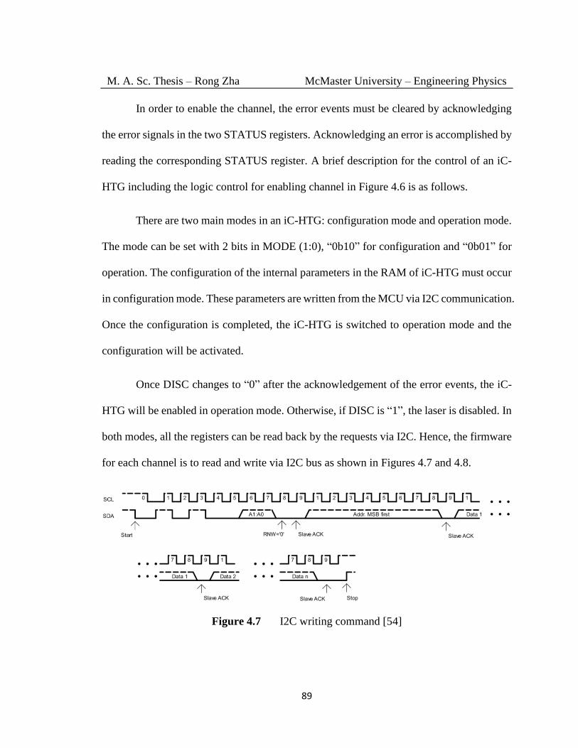
M. A. Sc. Thesis – Rong Zha McMaster University – Engineering Physics
89
In order to enable the channel, the error events must be cleared by acknowledging
the error signals in the two STATUS registers. Acknowledging an error is accomplished by
reading the corresponding STATUS register. A brief description for the control of an iC-
HTG including the logic control for enabling channel in Figure 4.6 is as follows.
There are two main modes in an iC-HTG: configuration mode and operation mode.
The mode can be set with 2 bits in MODE (1:0), “0b10” for configuration and “0b01” for
operation. The configuration of the internal parameters in the RAM of iC-HTG must occur
in configuration mode. These parameters are written from the MCU via I2C communication.
Once the configuration is completed, the iC-HTG is switched to operation mode and the
configuration will be activated.
Once DISC changes to “0” after the acknowledgement of the error events, the iC-
HTG will be enabled in operation mode. Otherwise, if DISC is “1”, the laser is disabled. In
both modes, all the registers can be read back by the requests via I2C. Hence, the firmware
for each channel is to read and write via I2C bus as shown in Figures 4.7 and 4.8.
Figure 4.7 I2C writing command [54]

M. A. Sc. Thesis – Rong Zha McMaster University – Engineering Physics
90
Figure 4.8 I2C reading command [54]
Figures 4.9 and 4.10 show a start-up sequence and the testing firmware
implemented in an MSP-EXP430G2GET launchpad. The setting for the LDD channel is
stored in an array of “conf []”. Its value is for testing purpose only.
The code is designed for the subprocess “Enable with the pre-configuration” for the
standalone configuration. In the first configuration, the LDD channels are enabled by the
commands from the host computer, the array of “conf []” for LDD parameters is updated
by decoding these commands in the next section.

M. A. Sc. Thesis – Rong Zha McMaster University – Engineering Physics
91
Start
Write configuration mode
Addr:0x1C
Read statusAddr:
0x00 and 0x01
Write channel configuration
registerAddr:0x10
Write channel OVC configuration
registerAddr:0x11
Configuring the output current
Value Addr:0x13-0x14
Set Current gain:CGAIN(1:0)
Addr:0x15
Enable output current DISC=0
Write operation mode
Addr:0x1C
Initialize I2C
END
Figure 4.9 Start-up sequence for the iC-HTG in each channel
//******************************************************************
//Test program of the start-up sequence of iC-HTG for standalone configuration;
//conf[] is the configurating data either decoded from instructions received in the
//UART in the first configuration; or a pre-setting value in the second configuration.
// Energia uses 7-bit address without RW bit: 0x50-0x57 for LDD0-LDD7
// Code is tested in Energia 1.8.7E21
//*********************************************************************
#include <Wire.h>
#define address 0x50 //LDD0

M. A. Sc. Thesis – Rong Zha McMaster University – Engineering Physics
92
#define conf_mode 0x02
#define oper_mode 0x01
byte conf[] = {0x8F, 0xFF, 0x00, 0x40, 0xFF, 0x00}; // values for testing purpose only
void setup()
{
Wire.begin(); // join i2c bus (address optional for master);
// ************configuration mode “10” ***********************************
Wire.beginTransmission(address); //sending an instruction to this LDD address
Wire.write(byte(0x1C)); // sets register pointer to the command register (0x1C)
Wire.write(conf_mode); //write 0x02 to register (0x1C)
Wire.endTransmission(); // "Hang up the line"
//**************configure the laser channel*********************************
Wire.beginTransmission(address);
Wire.write(byte(0x10)); // sets register pointer to the command register (0x10)
Wire.write(conf,6); // write to registers from 0x10 to 0x15 with the data from conf[]
Wire.endTransmission();
//***************read back the configuration: optional************************
// Wire.beginTransmission(address);
// Wire.write(0x10);
// Wire.requestFrom(address, 6);
// if (6 <= Wire.available())
// {
// ; //add codes for echoing back for verification
// }
//
//****************set DISC bit to 0***************************************
Wire.beginTransmission(address);
Wire.write(byte(0x10));
Wire.write(0xF7&conf[0]);
//DISC = 0
Wire.endTransmission();
// ****************Operation mode: "01"**********************************
Wire.beginTransmission(address);
Wire.write(byte(0x1C));
Wire.write(oper_mode);
Wire.endTransmission();

M. A. Sc. Thesis – Rong Zha McMaster University – Engineering Physics
93
}
//**************************Read status**********************************
void loop()
{
Wire.beginTransmission(address);
Wire.write(0x00);
Wire.endTransmission(); // point to register @ 0x00 from address
Wire.requestFrom(address, 2); // request 2 bytes from the current register
if (2 <= Wire.available()) // if two bytes were received
{
status0 = Wire.read(); // read Status0 @0x00
}
}
Figure 4.10 A test program for the start-up sequence of an iC-HTG
4.4 Decoding
In the previous sections, the firmware for the UART and the I2C are implemented. In the
first configuration, the data received from the UART can not directly used in the I2C as
shown in Figure 4.11.
Figure 4.11 Decoding between UART and I2C
If the UART receives the command “0xA0” from the host computer, which asks to
turn on the LDD0 channel in Table 4.1, this command will need to be translated into I2C

M. A. Sc. Thesis – Rong Zha McMaster University – Engineering Physics
94
actions to control the iC-HTG in the LDD0 channel. Hence, decoding will be required for
this command.
Table 4.5 translates the commands and requests from UART in Table 4.2 into
writing and reading of I2C. Subprocess at Stage 3 in Figure 4.3 is unfolded by the decoding
in Figure 4.12.
Table 4.5 Decoding the commands and requests from UART to I2C
I2C (Write/Read) RAM value Function
0x50 W DISC = 0 Enable LDD0 channel
…
0x57 W DISC = 0 Enable LDD7 channel
0x50 W DISC = 1 Disable LDD0 channel
…
0x57 W DISC = 1 Disable LDD7 channel
0x50 W REF[10:0] =
data10 Set the current according to data10 for LDD0
…
0x57 W REF[10:0] =
data10 Set the current according to data10 for LDD7
0x50 W ILIM[8:0] =
data8
Set the current limit according to data8 for
LDD0
…
0x57 W ILIM[8:0] =
data8
Set the current limit according to data8 for
LDD7
0x50 R (addr8)* Request RAM register value @addr8 inside
the HTG in LDD0
…
0x57 R (addr8)* Request RAM register value @addr8 inside
the HTG in LDD7
0x50 - 0x57 W DISC = 0 Enable all the LDD channels: 0x25
0x50 - 0x57 W DISC = 1 Disable all the LDD channels: 0x26
0x50 - 0x57 W Pre-settings Load the pre-settings for RGB LDD: 0x99
*(addr8) is the value at addr8 address. “()” means fetching a RAM value at this address.

M. A. Sc. Thesis – Rong Zha McMaster University – Engineering Physics
95
UART --> I2C
Execute commands
by I2C
UART --> I2C
Execute requests
By I2C
Echo with(addr8)
Figure 4.12 Subprocess at Stage 3 in Figure 4.3
4.5 Protection for the LDs
In Figure 4.2, detection for open connection in the lasers is performed before enabling the
laser channel. A subroutine for this purpose is executed . Protection function remains in the
main loop of the flow chart.
The implemented algorithm is shown in Table 3.8. The MCU will compare the
voltages of 𝑉𝐷 and 𝑉𝑝𝑠 measured by an A/D converter inside an iC-HTG in each LDD
channel. These voltages are transmitted to the MCU by I2C.
𝑉𝐷 can also be used to measure the channel efficiency in the software, because the
external power supply is known.
𝜂 =𝑉𝑝𝑠 − 𝑉𝐷
𝑉𝑝𝑠 (4.2)

M. A. Sc. Thesis – Rong Zha McMaster University – Engineering Physics
96
4.6 Software in the host computer
The purpose of the application software in the host computer is to mimic the projector main
circuits, which connects to the RGB LDD via the UART. A computer with any UART
application software can be used.
4.7 Summary
There are two types of firmware in the MCU in this chapter. One is for an RGB LDD
controlled by commands and requests from the projector. Information for these instructions
are not officially available to us. Therefore, a host computer with UART to mimic
communication in the projector is used. The other is a standalone RGB LDD that does not
require external communication.
Both configurations have been designed in top-down approaches. For
systematically designing a new RGB laser projector, the first configuration is a better
choice. In our retrofitting application, the second configuration will be used.

M. A. Sc. Thesis – Rong Zha McMaster University – Engineering Physics
97
Chapter 5
Results and Conclusions
Experiments are performed to verify the hardware and software design to meet the target
specifications in Table 2.6. These specifications will be checked one by one in a pass-fail
form in the last section.
In this chapter, Section 5.1 presents the setup for the performance test. Section 5.2
lists the experimental performance of RGB LDD. The protection functions provided by the
hardware and the firmware are triggered and tested in Section 5.3. Section 5.4 shows the
implemented communication protocols by a logic analyzer. Section 5.5 demonstrates the
maximum current in the DPSSL channel. Section 5.6 analyzes the issues found in the
hardware and firmware during the experiments and concludes the chapter.
5.1 Experimental setup
Because the AC-DC power supply inside the projector can not be used in the retrofitted
laser projector. There are two devices connected to the RGB LDD: an external AC-DC
power supply, RGB LDs. RGB LDD do not need UART communication in this application.
An RSP-750-24 AC-DC power supply from MEAN Well company is used. The
output current can achieve 31.3 A under 24 V output voltage with a maximum output power
of 750 W. But there is no display panel for the output current and voltage in this power
supply. To solve this issue, a 3003B bench power supply from Protek, which can provide
up to 3 A current under 24 V voltage, is used for testing each RGB channel respectively.

M. A. Sc. Thesis – Rong Zha McMaster University – Engineering Physics
98
In order to test and record experimental data for the performance of the RGB LDD,
a dummy load will replace LDs in the experiment. DL3021A from RIGOL, a
programmable DC electronic load works as RGB LDs connected between the anode and
the cathode in different RGB channels.
The assembled RGB LDD is shown in Figure 5.1. The MCU module is installed
separately. Five RGB and one DPSSL channels are tested. Two red (Channel 4 and 7) and
two green channels (Channel 5 and 6) are in the top row. One blue channel (Channel 3)
using a red wire to bypass a predesigned DC/DC is at the bottom-right. One DPSSL channel
(Channel 2) with a DC/DC is at second from the left, bottom row.
Two Oscilloscopes and a bench multimeter are used for monitoring the current and
voltage in the LDD channels during the test.
Figure 5.1 Top view of assembled RGB LDD

M. A. Sc. Thesis – Rong Zha McMaster University – Engineering Physics
99
Figure 5.2 Bottom view of assembled RGB LDD
An experimental setup for testing RGB channels is shown in Figure 5.3. MCU is
not included in the PCB of RGB LDD for three reasons:
1. An MCU board with power regulators can provide safe and stable 24 V to 3.3 V
conversion. An iC-HTG can provide a typical 3.3 V power for the MCU by its pin
of VDD, the output of its internal power regulator. This voltage can be as high as 5
V from the datasheet [54]. But most 3.3 V MCUs can not work at 5 V.
2. It is convenient to move around and load the debugging programs into a small size
one of 3.3 cm * 3.3 cm, rather than to carry a heavy big piece of PCB.
3. This MCU board is used in the previous projects and the function of the hardware
circuits has been verified. It can help to identify the location of the faulty circuit
during soldering and assembling.

M. A. Sc. Thesis – Rong Zha McMaster University – Engineering Physics
100
Figure 5.3 Experimental setup for testing the performance of the RGB LDD
On the other hand, the RGB LDD with UART communication aims to develop a
new RGB laser projector in the future. The external AC-DC power supply will not be
necessary because the power unit is pre-designed for RGB LDD inside the projector. The
communication function is tested by a logic analyzer with captured UART data at
“COMM1” and I2C data at “COMM2” as shown in Figure 5.3.
5.2 Experimental results of performance
5.2.1 Accuracy of the driving current
Figure 5.4 (a) shows the current in red and green channels calculated by Equation 3.9 with
𝑅𝑀𝐶 of 300 𝑚Ω and 𝐶𝑔 of 2. The maximum current value of 1.8438 A is generated by
inputting 10-bit “1”, i.e., 1023 in decimal, to the REF (10:0) register. The minimum current

M. A. Sc. Thesis – Rong Zha McMaster University – Engineering Physics
101
0.1671 A is acquired by inputting “0” to this register. Smaller current for better accuracy
can be obtained by increasing 𝐶𝑔. Similarly, (b) is the calculated current values ranging
from 0.2505 A to 2.766 A for the blue channel with 𝑅𝑀𝐶 of 200 𝑚Ω.and the same 𝐶𝑔.
For D/A converters, 1 least significant bit (LSB) in the input digital number
corresponds to the height of the smallest step between successive analog outputs. It is used
to describe the quantization error in the linear D/A converter. For the logarithmic D/A
converter, 1 LSB represents higer step value in the higer current range because of the
logarithmic curve according to Equation 3.9 as shown in Figures 5.4.
(a)
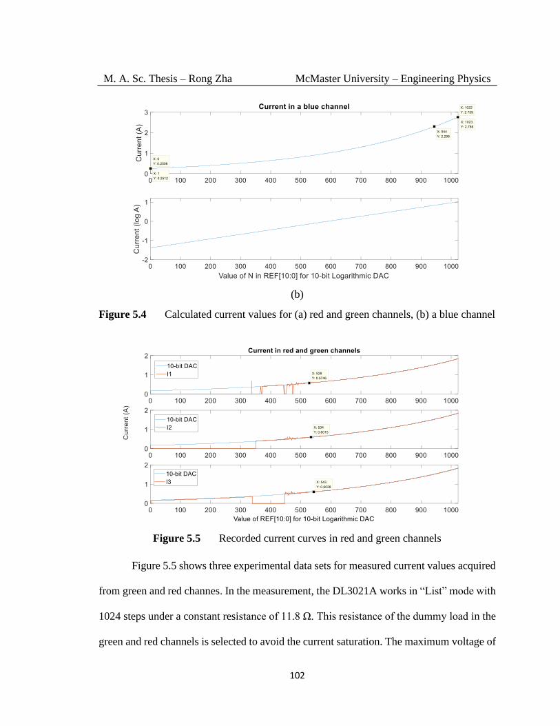
M. A. Sc. Thesis – Rong Zha McMaster University – Engineering Physics
102
(b)
Figure 5.4 Calculated current values for (a) red and green channels, (b) a blue channel
Figure 5.5 Recorded current curves in red and green channels
Figure 5.5 shows three experimental data sets for measured current values acquired
from green and red channes. In the measurement, the DL3021A works in “List” mode with
1024 steps under a constant resistance of 11.8 Ω. This resistance of the dummy load in the
green and red channels is selected to avoid the current saturation. The maximum voltage of

M. A. Sc. Thesis – Rong Zha McMaster University – Engineering Physics
103
less than 22 V across this dummy load will not exceed the compliance voltage. A test
program decreases N value in REF[10:0] register from 1023 to 0 while DL3021A records
1024 current values. As shown in Figure 5.5, DL3201A becomes ustable when the current
falls below about 0.6 A. Therefore, the following analysis for the acurracy bases on the
validated data above 0.6 A
Figure 5.6 Quantization errors in red and green channels
Figure 5.6 shows the 1 LSB quantization error in red and green channels. In the
measurement, the curves of current error is generated by subtracting the calculated values
from the measured values. As shown in Figure 5.6, the upper and bottom boundaries in y-
axis for current error are ± 0.0184 A since the targeting acurracy is 1%. .It is verified that
the current ranging from 0.6028 A to 1.844 A in red and green channels meets the
specification for accuracy. Current values of 1.3 A for red LDs and of 1.6 A for green LDs
will be used in our application.

M. A. Sc. Thesis – Rong Zha McMaster University – Engineering Physics
104
Figure 5.7 Recorded current curves in a blue channel
Figure 5.8 Quantization errors in a blue channel
Figure 5.7 shows more data is lost in blue channel than in red and green channels.
Logarithmic values of the current can eliminate these outliers. In the measurement, the
remaining current values are used to evaluate the blue channel. Similar as Figure 5.6, Figure
5.8 shows the quantization error for each digital value of N in the blue channel with y axis

M. A. Sc. Thesis – Rong Zha McMaster University – Engineering Physics
105
boundaries of ± 0.0276 A. The results also confirm that the design can fullfill the
requirement of the acurracy in the blue channel. Current value of 2.3 A will be used to drive
the blue LDs.
The outliers are filtered out in the analysis. The filtering of the outliers in the blue
channel is justified by the measurement of an oscilloscope for the whole range of the current.
Figure 5.9 shows the current waveforms, which are calculated by the measured waveforms
of the voltage dividing the dummy load resistance of 7.220 Ω. However, the precision is
lower than 0.8% (0.2 V resolution for 5 V/div under Full scale 7.22 Ω * 2.766 A) in the
measurement of the voltage by the oscilloscope, which is not high enough for the evaluation
of 1% accuracy. Therefore, the current waveform acquired from the oscilloscope is only
for the supplemental verification for the measurement from DL3021A. As shown in Figure
5.9, the measurement in Figure 5.8 is validated.
Figure 5.9 Current in a blue channel measured by an oscilloscope

M. A. Sc. Thesis – Rong Zha McMaster University – Engineering Physics
106
5.2.2 Compliance voltage
The compliance voltage for the current is acquired by increasing the resistance in DL3021A
until the current is saturated and decreased. Data are recorded by a USB memory stick.
The MCU is preloaded a test program that enables the channel to output the specific
current values. Figure 5.10 shows the compliance voltage for the current of 1.3 A. In the
measurement, five datasets for the current and voltage are recorded. As shown in Figure
5.10, the compliance voltage of 23.14 V meets the requirements in the target specifications.
Similar results are shown in Figures 5.11 and 5.12. Both fulfill the requirements. Because
the next section will test the stability of the current, these figures do not include the error
bars.
Figure 5.10 Compliance voltage for current of 1.3 A
23.1403, 1.3007
1
1.05
1.1
1.15
1.2
1.25
1.3
1.35
14 15 16 17 18 19 20 21 22 23 24
Cu
rren
t (A
)
Voltage (V)
Compliance voltage at 1.3 A
I1 I2 I3 I4 I5

M. A. Sc. Thesis – Rong Zha McMaster University – Engineering Physics
107
Figure 5.11 Compliance voltage for current of 1.6 A
Figure 5.12 Compliance voltage for current of 2.3 A
5.2.3 Current stability
The stability of the current for driving RGB LDs are tested in three specific values: red
channel of 1.3 A, green channel of 1.6 A and blue channel of 2.3 A.
1.6006 1.5994 1.5987 23.032, 1.5997
1.35
1.4
1.45
1.5
1.55
1.6
1.65
15 16 17 18 19 20 21 22 23 24
Cu
rren
t (A
)
Voltage (V)
Compliance voltage at 1.6 A
I1 I2 I3 I4 I5
2.2986 23.0489, 2.2985
2.1
2.15
2.2
2.25
2.3
2.35
14 15 16 17 18 19 20 21 22 23 24
Cu
rren
t (A
)
Voltage (V)
Compliance voltage at 2.3 A
I1 I2 I3 I4 I5

M. A. Sc. Thesis – Rong Zha McMaster University – Engineering Physics
108
Figure 5.13 Current stability at 1.3 A in a red channel
Figure 5.14 Current stability at 1.6 A in a green channel
1.29771.2977
1.2977
1.2955
1.2977
1.295
1.2955
1.296
1.2965
1.297
1.2975
1.298
0 1000 2000 3000 4000 5000 6000
Cu
rren
t (A
)
Sampling number
1.3 A in red channels
1.6016
1.59931.599
1.5995
1.6
1.6005
1.601
1.6015
1.602
0 1000 2000 3000 4000 5000 6000 7000 8000
Cu
rren
t (A
)
Sampling number
1.6 A in green channels

M. A. Sc. Thesis – Rong Zha McMaster University – Engineering Physics
109
Figure 5.15 Current stability at 2.3 A in a blue channel
Figure 5.13 shows the stability for the current of 1.3 A in a red channel. In the
measurement, DL3021A is used to record the data of the current for about 25 minutes. As
shown in Figure 5.13, the ratio of variation in the current is within 0.3%. The result is better
than the target specification. Figures 5.14 and 5.15 show the stability for the current of 1.6
A and 2.3 A in green and blue channels respectively. Similarly, both results for the stability
meet the requirements as shown in the figures.
5.3 Experimental results of protection
5.3.1 Tun-on delay and power on-off
Figure 5.16 shows the waveforms captured from turning the power on to off. In the
measurement, a dummy load of 14 Ω is connected between the terminals of the anode and
the cathode in a green LDD channel, yellow curve measuring the voltage from the anode
and purple curve showing the voltage from the cathode. As shown in Figures 5.16, the first
2.2988
2.3009
2.2985
2.299
2.2995
2.3
2.3005
2.301
2.3015
0 1000 2000 3000 4000 5000 6000 7000 8000
Cu
rren
t (A
)
Sampling number
2.3 A in a blue channel

M. A. Sc. Thesis – Rong Zha McMaster University – Engineering Physics
110
rising slopes of both yellow and purple curves are generated by turning on the external
power supply. Then two curves maintain the maximum value of 24 V for about 2.5 s.
During this period, two terminals of the load have the same voltage because the channel is
disabled with no current flowing through the load. Turn-on delay of 2.5 s fulfills the FDA’s
regulation. As shown in Figure 5.17, soft-start of 156.4 ms is generated by the purple curve
ramping down until the voltage drop reaches about 12.7V. Current of 0.9 A flows through
14 Ω load.
Figure 5.16 On-off of the power
Figure 5.17 Soft-start of current of 0.9 A
In general, directly power off without disabling the channel output is not allowed
in the LDDs, a reverse current may be generated as shown in Figure 3.20. Figures 5.18 and
5.19 shows the captured waveforms from a normal LDD channel and a saturated LDD
channel in the power off events respectively. In order to intentionally generate a saturated
LDD channel, the current of 1.8A through two resistors of 7 Ω in series is configurated. If
the channel was not saturated, the voltage across the load would be higher than 24 V. The
measured current is saturated at 1.55 A. Figure 5.19 shows the two waveforms from the
terminals of the high side 7 Ω resistor. As shown in both figures, no reverse voltage and
spikes of the current are found.

M. A. Sc. Thesis – Rong Zha McMaster University – Engineering Physics
111
Figure 5.18 Power off a normal channel
Figure 5.19 Power off a saturated channel
In order to analyze the these curves, four zones are used to describe the power-off
event in the channel with normal or saturated current.
1. Both yellow and purple curves fall while the voltage drop between them still
maintains constant after powering off. Current remains constant. As shown in
Figure 5.19, this period will not appear in the saturated channel.
2. Purple curve flats out at a low voltage. Consequently, the voltage between two
curves drops and current begins to decrease.
3. Purple curve rises when the yellow curve falls below 3V. A power-down error is
triggered when the power supply of iC-HTG drops below 3V. This error will disable
the LDD by turn off the N MOSFET in the channel. Hence, purple curve will rise
to the yellow curve because there is no current flow through the loads between them.
4. Purple curve follows the yellow curve until power is completely off.
5.3.2 OCP by the iC-HTG
Figure 5.20 shows OCP with current limit of 1.6 A triggered from 1.3 A current in a red
LDD channel. In the measurement, two dummy loads of 7 Ω are connected in series. OCP
is performed without the crowbar circuits across the test loads. Yellow curve of CH1 is the
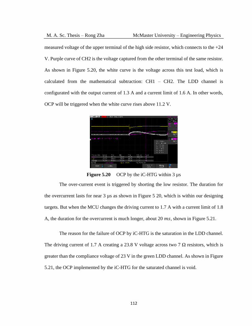
M. A. Sc. Thesis – Rong Zha McMaster University – Engineering Physics
112
measured voltage of the upper terminal of the high side resistor, which connects to the +24
V. Purple curve of CH2 is the voltage captured from the other terminal of the same resistor.
As shown in Figure 5.20, the white curve is the voltage across this test load, which is
calculated from the mathematical subtraction: CH1 – CH2. The LDD channel is
configurated with the output current of 1.3 A and a current limit of 1.6 A. In other words,
OCP will be triggered when the white curve rises above 11.2 V.
Figure 5.20 OCP by the iC-HTG within 3 µs
The over-current event is triggered by shorting the low resistor. The duration for
the overcurrent lasts for near 3 µs as shown in Figure 5 20, which is within our designing
targets. But when the MCU changes the driving current to 1.7 A with a current limit of 1.8
A, the duration for the overcurrent is much longer, about 20 𝑚𝑠, shown in Figure 5.21.
The reason for the failure of OCP by iC-HTG is the saturation in the LDD channel.
The driving current of 1.7 A creating a 23.8 V voltage across two 7 Ω resistors, which is
greater than the compliance voltage of 23 V in the green LDD channel. As shown in Figure
5.21, the OCP implemented by the iC-HTG for the saturated channel is void.

M. A. Sc. Thesis – Rong Zha McMaster University – Engineering Physics
113
Figure 5.21 OCP by the iC-HTG in a saturated LDD channel
5.3.3 Crowbar circuits
The speed of shunting action of the crowbar circuits is tested under two conditions: one is
shunted without disabling the LDD channel, the other is shunted while disabling the LDD
channel. The first shunting action can be used for pulsing the LDs in the future. The second
one is for the OCP of LDs.
The setup for this test is similar as the OCP by iC-HTG in green/red channels. The
blue channel is used for the crowbar test.
In order to protect the LDs in all the over-current events, the fast shunting speed of
the crowbar is a must. A test program for simulating error events is designed for iC-HTG
in the blue LDD channel, which is used to evaluate this shunting speed. As shown in the
previous Figure 4.6, writing “1” to the bit “SOVC” at 0x16 in the RAM generates an over-
current error signal which will disable the LDD channel; and writing “1” to the bit
“S0SCERR” in the same register will generate an oscillator’s error signal without affecting
the channel status. Both error signals will pull “NCHK” pin down to the ground, activating
the crowbar’s shunting action.

M. A. Sc. Thesis – Rong Zha McMaster University – Engineering Physics
114
(a) (b)
Figure 5.22 Crowbar circuits acting under the simulating error events: (a) “SOVC” and
(b) “SOSCERR”
Figure 5.22 shows the shunting action of the crowbar circuits. In the measurement,
A four-channel “WAVERUNNER” oscilloscope shows all the waveforms. Curve 2 is the
voltage of “NCHK”, and curve D is the calculated voltage (CH3 – CH1) across the high
side load of 7 Ω. This configuration of measurement is used for all the OCP with crowbar
circuits. As shown in Figure 5.22 (a), “NCHK” is activated by “SOVC”, the shunting action
completed within 1.25 µs. The duration of the shunting action triggered by “SOSCERR” is
about 1.5 µs as shown in Figure 5.22 (b). The simulation shows that the shunting action for
OCP can meet the requirement. However, the delay from detection of error events by the
iC-HTG to activation of “NCHK” signal can not be simulated.
In the real applications, an over-current event happens before “NCHK” pulls down.
Two scenarios for over-current events are presented as below.
Figure 5.23 shows OCP with crowbar circuits for a normal LDD channel. In the
measurement, the current is set to be 1.3 A with an over-current limit of 1.6 A (11.2 V in

M. A. Sc. Thesis – Rong Zha McMaster University – Engineering Physics
115
the D curve) as shown in Figure 5.23 (a). The duration for the over-current is around 1.3
µs. The current is set to be 1.5A with an over-current limit of 1.8 A (12.6 V in the D curve)
as shown in Figure 5.23 (b). The duration for the over-current is about 1.5 µs. There are
two stages for activating the protection as shown in both figures.
1. Before “NCHK” is pull down, the OCP is implemented by the iC-HTG,
which is discussed in the previous section. Figure 5.23 (a) shows this OCP
effectively reduces the duration of the over-current period. The OCP in
Figure 5.23 (b) works but does not decrease the current under the over-
current limit.
2. After “NCHK” is pull down, the shunting action of the crowbar circuits is
activated. The acceleration for turning off the current is appeared in both
figures, which enable the OCP to be completed within 1.5 µs shown in
Figure 5.23 (b).
(a) (b)
Figure 5.23 OCP with the crowbar circuits

M. A. Sc. Thesis – Rong Zha McMaster University – Engineering Physics
116
OCP for the first scenario meets the target specification when the channel is not
saturated. And OCP by the crowbar circuits may reduce the over-current duration further.
The second scenario is OCP for a saturated channel. As shown in the previous
section, OCP by the iC-HTG fails to meet the specification under this condition. Figure
5.24 shows OCP with crowbar circuits in the saturated blue LDD channel. In the
measurement, the current is set to be 2.3 A with an overcurrent limit of 2.6 A (18.2 V in
the D curve). The driving current multiplying the total resistance of 14.78 Ω (0.78 Ω is the
long wire resistance measured by a bench multimeter in 4-wire mode) will generate about
34V voltage, which is higher than the compliance voltage of the blue channel. As shown in
Figures 5.24 (a) and (b), the crowbar circuits help to effectively clamp the current under
the over-current limit. The duration of the over-current period is around 1.5 µs. OCP with
crowbar circuits for the saturated channel also meets the requirement.
(a) (b)
Figure 5.24 OCP with the crowbar circuits in a saturated blue channel (a) clamped
current lasts for 30 ms (b) 1.5 µs overcurrent period

M. A. Sc. Thesis – Rong Zha McMaster University – Engineering Physics
117
5.3.4 Relay
The shorting relay can be controlled by the MCU if jumper head “P4” is plugged as shown
in Figure 3.25. When the power of RGB LDD is on, the MCU opens all the relays by pulling
up the voltage of the control pin. These relays are driven by NUD3124s, which can be
directly controlled by the MCU output. These optional relays are only for ESD protection
when LDs are not used.
5.4 Experimental results of communication
LA5016 KINGST logical analyzer is used to present the experimental results for the
communications. Four input channels from LA5016 connected to the RXD and TXD from
UART (COMM1), SCLK and SDA from I2C (COMM2).
5.4.1 I2C
The parameters for RGB channels are all included in the program in the appendix. This
logic anlyzer use 8-bit address in Table 3.13 for I2C communication. Figure 5.25 shows
the MCU can not receive an acknowledging signal for Channel 0. Because Channel 0 is not
installed.
Figure 5.25 No acknowledgement from the empty Channel 0
Figure 5.26 Detection of open laser connection

M. A. Sc. Thesis – Rong Zha McMaster University – Engineering Physics
118
Figure 5.26 shows the detection of open laser connection in Channel 6. After power
is on, the LDD channel is disabled by default. The voltage of the cathode (“Vd”, discussed
in Section 3.3.4) is same as the voltage of anode if the connection is normal since there is
no current. As shown in Figure 5.26, a command of 0xE2 is written into the register at the
address of 0x10, enabling the 10-bit ADC to measure “Vd”. The high 2 bits of the ADC
measurement are stored in the bit-1 and bit-0 at the address of 0x03. The anode is connected
to 24 V, the measurement of “Vd” should be close to 699 (0x2BB) in normal connection
according to Equation 3.17 in Section 3.3.4. In other words, 0x02 will appear in the register
at the address of 0x03. Because the data read from the register at the address of 0x03 is
0x00 as shown in Figure 5.26, the open connection of the LDs is detected.
According to Table 3.13, Figure 5.27 shows the initializaion of Channel 4 for red
LDs; Figure 5.28 shows the initializaion of Channel 3 for blue LDs; Figure 5.29 shows the
initializaion of Channel 5 for green LDs. Taking Channel 4 for example, the writing and
reading sequences follow the descriptions in Figures 4.9 and 4.10. As shown in Figure 5.27,
four steps for initializing the iC-HTG in this LDD channel are listed.
1. In the first transmission, channel address of 0xA8, register address of 0x1C
and the data of 0x02 for the register are written. According to the functions
of the registers listed in [54], these three writing actions turn the iC-HTG
into “Configuration” mode.
2. In the second transmission, channel address of 0xA8, register address of
0x10, six data from 0xE7 to 0x00 are written. According to the functions of
register listed in [54], these written values shown in Figure 5.27 configurate

M. A. Sc. Thesis – Rong Zha McMaster University – Engineering Physics
119
the channel with a driving current of 1.3 A and a current limit of 1.6 A. The
10-bit ADC is enabled to measure the voltage form “ANIN”, etc.
3. The third transmission clears error bits in the status register by reading data
from this register. Figure 5.27 shows the channel address of 0xA8 and the
register address of 0x00 are written. The data from this register is read back
by a request. The detailed discussion is included in Section 4.3.
4. Final transmission turns this channel into “Operation” mode by writing data
of 0x01 to the same register in the first step. The LDD channel is ready for
the standalone application now.
Figure 5.27 Initialization in Channel 4
Figure 5.28 Initialization in Channel 3
Figure 5.29 Initialization in Channel 5
Therefore, requirements of I2C communication for the standalone application are
fulfilled.
As shown in Figure 5.30, a delay of 2 s before the start of I2C communication can
meet the FDA’s regulation for the slow turn-on of lasers.

M. A. Sc. Thesis – Rong Zha McMaster University – Engineering Physics
120
Figure 5.30 A delay of 2 s before the start of I2C communication
5.4.2 Decoding
The designed commands and requests from UART in Table 4.5 and their decoded I2C
actions are captured for analysis. All the tests are performed on Channel 6.
Figures 5.31 - 5.35 show the decoding for disabling Channel 6, enabling Channel 6,
changing driving current to 1.3 A, modifying the current limit to 1.6 A, requesting the data
of 0xDD from the register at the address of 0x11 respectively. As shown in these figures,
the commands and request are decoded successfully.
Figure 5.31 Command from UART: disable Channel 6
Figure 5.32 Command from UART: enable Channel 6

M. A. Sc. Thesis – Rong Zha McMaster University – Engineering Physics
121
Figure 5.33 Command from UART: Changing driving current in Channel 6
Figure 5.34 Command from UART: Changing current limit in Channel 6
Figure 5.35 Request from UART: Request data from address (0x11) in Channel 6
5.5 Experimental results of the DPSSL channel
The DPSSL channel in the RGB LDD is for the next phase, which can be an alternative for
the commercial DPSSL driver in the future.
As shown in Figure 5.36, Curve D is the voltage across a dummy load of 0.15 Ω in
the DPSSL channel, 6 A current with soft-start is generated. The resistance of RMC used
in the test is 0.8 Ω. Requirement for the DPSSL channel is fulfilled.

M. A. Sc. Thesis – Rong Zha McMaster University – Engineering Physics
122
(a) (b)
Figure 5.36 Current of 6 A in the DPSSL channel
5.6 Discussion and Summary
5.6.1 Problems and solutions
Conventional pull-up resistors of 4.7 kΩ can not be used in the I2C circuits. Otherwise, the
captured yellow waveform of SDA can not correctly decoded by the MCU as shown in
Figure 5.37. Using pull-up resistors of 1 kΩ for I2C can solve this problem.
Figure 5.37 Error in I2C due to the pull-up resistors

M. A. Sc. Thesis – Rong Zha McMaster University – Engineering Physics
123
The P MOSFETs in the crowbar circuits may need heatsinks to avoid the over-heat
during the shunting action, especially in a saturated LDD channel. Because the on-time for
the P MOSFET can be up to several tens of milliseconds. If the saturation of the channel is
avoided, this issue will not appear.
On the firmware side, disabling the interruption from I2C during the UART
communication is necessary. Otherwise, only the first byte data after the command from
the UART can be decoded into I2C communication. As shown in Figure 5.38, the second
data is lost. 0xC6 is the command of changing driving current in Channel 6 from UART,
followed by the 2 bytes data of 0x43 and 0x6A for setting a new driving current. Because
the speed of UART is lower than I2C. During the waiting period for the next available data
in UART, the I2C interruption will read a void data (0xFF) from the buffer of UART.
Figure 5.38 Error decoding due to the failure of fetching data from UART
5.6.2 Summary
Base on the experimental results, a pass/fail Table 5.1 is created according to Table 2.6.
The saturation of the LDD channel can be avoided if the forward voltage of LDs is lower
than the compliance voltage of the LDD channel. In this case, OCP by the iC-HTG is within
the specifications. And the detection for the channel saturation and the crowbar circuits
becomes redundant.

M. A. Sc. Thesis – Rong Zha McMaster University – Engineering Physics
124
Table 5.1 Pass/Fail table for target specifications
Specifications Pass/Fail
LDD output
performance
Maximum current (A)
R: 1.6; G: 1.8;
B: 2.7; DPSSL:
5.5
Pass
Compliance voltage (V)
Pass
Current stability 1% Pass
Current set accuracy 1% Pass
Protection for
the LD/LDs
Soft start for current Adjustable,
typical 100 mS Pass
Fast over current
protection (OCP) for
each channel
< 4 µS Pass
Reverse current
protection Pass
ESD and transient
protection Pass
Open laser protection Pass
Communication
Interface
UART: between the
projector and the LDD
Designed
protocol can be
compatible with
UHP driver
Pass
I2C: connecting all the
channels of the LDD to
a micro-controller
Pass
Dimensions < 40cm*40cm*8cm Pass

M. A. Sc. Thesis – Rong Zha McMaster University – Engineering Physics
125
Chapter 6
Conclusion and Future Research Direction
6.1 Conclusion
A linear RGB LDD for a laser projector has been designed, assembled and tested.
Electronic performance and the protection for LDs in each RGB LDD channel were
investigated in this thesis.
Electrical specifications of the developed RGB LDD have been confirmed from the
measurements. The developed RGB LDD will be used in a retrofitted RGB laser projector.
It has been shown that one LDD channel (#3) can provide 2.3 A current for five blue LDs
in series connection with 22 V forward voltage. Two LDD channels (#4 & #7) are able to
provide 1.3 A for driving ten red LDs in series with 22.5 V forward voltage in each channel;
and two other LDD channels (#5 & #6) can provide 1.6 A for driving four green LDs in
series with 18.8 V forward voltage in each channel. Compliance voltage of 23 V up to 2.3
A for all the RGB LDD channels avoids current saturation. Although it is not used in the
current application, the DPSSL channel with a DC/DC converter is reserved in our design.
A maximum current output of 6 A can be achieved.
In order to boost the efficiency for all the channels inside the RGB LDD, the voltage
of the LDs needs to be close to the compliance voltage of the LDD channel. We have used
the lowest forward voltage of 22 V from all five blue LDs connected in series to decide the
RGB LDD topology in the overall design for reducing the cost and increasing the total

M. A. Sc. Thesis – Rong Zha McMaster University – Engineering Physics
126
efficiency in Chapter 2. A bottom-up approach for hardware design and a top-down method
for firmware implementation have been demonstrated to fulfill the performance and
protection functions for the RGB LDDs, as shown in Chapter 3 and Chapter 4 respectively.
Two scenarios for designing the LDD driver for RGB laser projector have been discussed.
One is retrofitting from a lamp-based projector with a standalone RGB LDD and the other
is developing a new RGB laser projector with an integrated RGB LDD controlled by UART
communication. The developed RGB LDD with UART interface can maintain compatible
with the communication protocols in the previous lamp driver.
As shown in Chapter 5, experimental results have verified the performance and
protection functions of the developed RGB LDD as well as the communication functions.
For performance, it has been shown that the developed RGB LDD can achieve a maximum
of 1.8 A current for red/green channels and 2.7 A current for the blue channel. The recorded
data has shown that accuracy within 1% and working current stability under 1% can be
achieved for all the channels. For protection, it was found that the OCP has a response time
within 1.5 µs, implying that the protection for the LDs during the overcurrent event can be
effective. Safety for the LDs during on-off action of the power can be guaranteed. The open
laser connection can be detected before enabling the LDD channels. For communications,
UART and I2C have been analyzed and presented by a logical analyzer.

M. A. Sc. Thesis – Rong Zha McMaster University – Engineering Physics
127
6.2 Future research direction
In this thesis, it has been demonstrated that there is still room for improving the DPSSL
channel. It is necessary to combine a temperature controller, like a TEC controller within
the DPSSL channel in case the passive cooling for DPSSL is not enough.
This thesis did not consider the optical feedback, which would enable the detection
of damaged or degraded LDs. We have found that some damaged red LDs do not change
their I-V curves, which means there is no way to detect this damage by using an electronic
method. Fault detection via photo-diodes in RGB LDD can be more effective. However,
this method suffers from the interference from multiple LDs. To identify the light from a
specific LD is very difficult in the current projector configuration.
Another idea worth to exploring is to use an iC-HTG to directly regulate a
commercial DC/DC to build an LDD channel, if the ripple from DC/DC can be effectively
reduced. It might be a good candidate for implementing a new multi-channel RGB LDD
since modern technology for DC/DC can significantly shrink LDD size while maintaining
its high efficiency.

M. A. Sc. Thesis – Rong Zha McMaster University – Engineering Physics
128
References
[1] Weichmann, Ulrich, et al. "UHP lamps for projection systems: getting always
brighter, smaller, and even more colorful." Liquid Crystal Materials, Devices, and
Applications X and Projection Displays X 5289 (2004): 255-266.
[2] Brennesholtz, Matthew S., and Edward H. Stupp. Projection displays. Vol. 19. John
Wiley & Sons, 2008., pp 170
[3] Fischer, E. "Ultra High-Performance Discharge Lamps for Projection TV Systems,
8th Int." Symp. on Light Sources, Greifswald, Germany. 1998.
[4] Moench, H., and G. Derra. "Light sources for video projection 8th Int." Symp. on
Light Sources, Greifswald, Germany. 1998.
[5] Fischer, Hanns E., and Horst Horster. "High-pressure mercury vapor discharge
lamp." U.S. Patent No. 5,109,181. 28 Apr. 1992.
[6] Flesch, Peter (2006). Light and Light Sources: High-intensity Discharge Lamps.
Springer. p. 39. ISBN 9783540326854.
[7] Moench, H., et al. "52.1: Invited Paper: New Developments in Projection Light
Sources—Shorter Arcs and Miniaturisation." SID Symposium Digest of Technical
Papers. Vol. 32. No. 1. Blackwell Publishing Ltd, 2001.
[8] Derra, Guenther, et al. "UHP lamp systems for projection applications." Journal of
Physics D: Applied Physics 38.17 (2005): 2995.
[9] Heusler, Gero, et al. "Advanced UHP lamps for projection systems." Projection
Displays IX 5002 (2003): 20-31.

M. A. Sc. Thesis – Rong Zha McMaster University – Engineering Physics
129
[10] Mönch, Holger, et al. "9.1: Arc Stabilisation for Short Arc Projection Lamps." SID
Symposium Digest of Technical Papers. Vol. 31. No. 1. Oxford, UK: Blackwell
Publishing Ltd, 2000.
[11] Projector Central.COM “Find a Projector”. 19 June. 2019:
https://www.projectorcentral.com/
[12] Jansen, M., et al. "Visible laser sources for projection displays." Projection
Displays XII. Vol. 6489. International Society for Optics and Photonics, 2007.
[13] Barco Corporation. “Flagship Laser cinema projectors”. 19 June. 2019:
https://www.barco.com/en/products/flagship-laser-cinema-projectors
[14] RGB laser projection. 19 June. 2019: https://www.christiedigital.com/en-
us/display-technology/laser-projection/rgb-laser-projection
[15] Perkins, Michael, and Alen Koebel. "36‐2: Invited Paper: Lasers, Lamps, or
Phosphors–Choices for the Future of Digital Cinema." SID Symposium Digest of
Technical Papers. Vol. 48. No. 1. 2017.
[16] NecDisplay. “Higher Education”. 19 June. 2019:
https://www.necdisplay.com/laser-projectors/applications.html
[17] BenQ. “The Three Reasons You Need a Laser Projector in Your Conference
Room”. 19 June. 2019: https://business-display.benq.com/en-ap/explore/trends/3-
reasons-you-need-a-laser-projector.html
[18] Panasonic Corporation. “Introducing Solid Shine Laser Technolog”.19 June.
2019: https://panasonic.net/cns/projector/solution/technology/laser/

M. A. Sc. Thesis – Rong Zha McMaster University – Engineering Physics
130
[19] CASIO. “TCO Calculator”. 19 June. 2019: https://www.casio-lampfree-
projectors.com/en/tco/.
[20] Epson. “Laser Projectors”. 19 June. 2019: https://epson.ca/laser-projectors.
[21] Basu, Chandrajit, Merve Meinhardt-Wollweber, and Bernhard Roth. "Lighting
with laser diodes." Advanced Optical Technologies 2.4 (2013): 313-321.
[22] Svilainis, Linas. "LEDs for projectors." Nitride Semiconductor Light-Emitting
Diodes (LEDs). Woodhead Publishing, 2018. 737-760.
[23] Janssens, Peter, and Koen Malfait. "Future prospects of high-end laser
projectors." Emerging Liquid Crystal Technologies IV. Vol. 7232. International
Society for Optics and Photonics, 2009.
[24] BT.2020. Parameter values for ultra-high definition television systems for
production and international programme exchange. 19 June. 2019:
https://www.itu.int/rec/R-REC-BT.2020-2-201510-I/en
[25] Candry, Patrick, and Bart Maximus. "Projection displays: New technologies,
challenges, and applications." Journal of the Society for Information Display 23.8
(2015): 347-357.
[26] Murayama, Masahiro, et al. "Watt‐class green (530 nm) and blue (465 nm) laser
diodes." physica status solidi (a) 215.10 (2018): 1700513.
[27] Masui, S. "Watt-level Green/Blue Laser Diodes." The 4th Laser Display and
Lighting Conference (LDC2015), LD&LE. 2015.
[28] Nakamura, Shuji, Stephen Pearton, and Gerhard Fasol. The blue laser diode: the
complete story. Springer Science & Business Media, 2000.

M. A. Sc. Thesis – Rong Zha McMaster University – Engineering Physics
131
[29] Li, Shuxing, et al. "Color Conversion Materials for High‐Brightness Laser‐
Driven Solid‐State Lighting." Laser & Photonics Reviews 12.12 (2018): 1800173.
[30] Simon Cohen and Caleb Denison. Is Hisense’s 100-inch, RGB three-laser TV the
ultimate home theater centerpiece? 8 Jan. 2019:
https://www.digitaltrends.com/home-theater/hisense-rgb-three-laser-tv-ultra-short-
throw-projector-ces-2019/
[31] Nagahara, Seiji. "8‐1: Three Primary Color LD Module." SID Symposium
Digest of Technical Papers. Vol. 48. No. 1. 2017.
[32] Wallon, J., et al. "Sensitivity to electrostatic discharges of “low-cost” 1.3 μm
laser diodes: a comparative study." Materials Science and Engineering: B 28.1-3
(1994): 314-318.
[33] Magistrali, F., et al. "ESD induced degradation mechanisms of InGaAsP/InP
lasers." Quality and reliability engineering international 8.3 (1992): 287-293.
[34] Twu, Y., et al. "Semiconductor laser damage due to human-body-model
electrostatic discharge." Journal of applied physics 74.3 (1993): 1510-1520.
[35] Huang, Jia-Sheng, Todd Olson, and Eric Isip. "Human-body-model electrostatic-
discharge and electrical-overstress studies of buried-heterostructure
semiconductor lasers." IEEE Transactions on Device and Materials Reliability 7.3
(2007): 453-461.
[36] DeChairo, L. F., and B. A. Unger. "Degradation in InGaAsP semiconductor
lasers resulting from human body model ESD." Journal of electrostatics 29.3
(1993): 227-250.

M. A. Sc. Thesis – Rong Zha McMaster University – Engineering Physics
132
[37] Ichikawa, Hiroyuki, et al. "Analysis of Reverse-Biased Electrostatic-Discharge-
Induced Degradation of GaInAsP/InP Buried Heterostructure Laser Diode."
Japanese Journal of Applied Physics 48.2R (2009): 022201.
[38] Tang, W. C., et al. "Evidence for current‐density‐induced heating of AlGaAs
single‐quantum‐well laser facets." Applied physics letters 59.9 (1991): 1005-
1007.
[39] Sim, S. P., M. J. Robertson, and R. G. Plumb. "Catastrophic and latent damage in
GaAlAs lasers caused by electrical transients." Journal of applied physics 55.11
(1984): 3950-3955.
[40] B. Dobkin, J. Williams, and J. Williams, “Current sources for fiber optic lasers:
A compendium of pleasant current events,” Analog Circuit Des., pp. 319–337,
Jan. 2011.
[41] D. Hodgson and B. Oslen. “Protecting your laser diode”, Sept. 2003:
https://www.newport.com/medias/sys_master/images/images/hc0/h01/879704945
4622/AN03-Protecting-Your-Laser-Diode.pdf
[42] Tomm, Jens W., et al. "Mechanisms and fast kinetics of the catastrophic optical
damage (COD) in GaAs‐based diode lasers." Laser & Photonics Reviews 5.3
(2011): 422-441.
[43] Wikipedia. “IEEE-488”. 19 June. 2019: https://en.wikipedia.org/wiki/IEEE-488
[44] National Instruments. “What Is LabVIEW?”. 19 June. 2019:
https://www.ni.com/en-ca/shop/labview.html

M. A. Sc. Thesis – Rong Zha McMaster University – Engineering Physics
133
[45] NEC Display Solutions Europe. “Laser Technologies” 19 June. 2019:
https://www.nec-display-solutions.com/p/laser/en/technologies.xhtml
[46] USHIO OPTO. “HL63283HD 637nm /1.2W (CW) /1.5W (Pulse)
AlGaInP Laser Diode”. 19 June. 2019: https://www.ushio-
optosemi.com/documents/uos/products/UOSE_DS_HL63283HD_R2.pdf
[47] Xu, Binbin, et al. "High-power broadly tunable grating-coupled external cavity
laser in green region." Review of Scientific Instruments 89.12 (2018): 125106.
[48] Peng, Jue, et al. "3.1 W narrowband blue external cavity diode laser." Young
Scientists Forum 2017. Vol. 10710. International Society for Optics and
Photonics, 2018.
[49] Analog Technologies, Inc. “Why and How Should We Choose A Constant
Current Laser Driver” 03 Aug. 2018: http://www.analogtechnologies.com/white-
paper/2018/0803/1087.htm
[50] Wikimedia Commons. “File: I vs V mosfet.png”. 3 Jan. 2015:
https://commons.wikimedia.org/wiki/File:IvsV_mosfet.png
[51] On Semiconductor.” FQPF45N15V2-D”. Oct. 2013:
https://www.onsemi.com/pub/Collateral/FQPF45N15V2-D.pdf
[52] iC-Haus. “Discrete vs. Integrated: Driving laser diodes with discrete or integrated
circuits?” N.D.: http://ichaus.de/upload/pdf/Appl3_a3es.pdf
[53] iC-Haus. “Design and Test of Fast Laser Driver Circuits”. N.D.:
https://www.electrooptics.com/sites/default/files/content/white-
paper/pdfs/DesignTestFastLaserDriverWP4en_mz-12032012a.pdf

M. A. Sc. Thesis – Rong Zha McMaster University – Engineering Physics
134
[54] iC-Haus. “iC-HTG POWER CW LASER DIODE DRIVER Rev A1”. N.D.:
https://www.ichaus.de/upload/pdf/HTG_datasheet_A1en.pdf
[55] Erickson, Christopher J., et al. "An ultrahigh stability, low-noise laser current
driver with digital control." Review of Scientific Instruments 79.7 (2008): 073107.
[56] Opt Lasers. “4 W RGB Laser Module v2 + PSU”. 19 June. 2019:
https://optlasers.com/rgb-modules/4w-rgb-laser-module-v2
[57] Digi-Key Electronics. “Transistors - FETs, MOSFETs – Single”. 19 June. 2019:
https://www.digikey.ca/products/en/discrete-semiconductor-products/transistors-
fets-mosfets-single/278?k=mosfet
[58] U.S. Food & Drug Administration. “CFR - Code of Federal Regulations Title
21”. 1 April. 2018:
https://www.accessdata.fda.gov/scripts/cdrh/cfdocs/cfcfr/CFRSearch.cfm?FR=104
0.10
[59] Vishay Siliconix. “Power MOSFET Basics: Understanding Gate Charge and
Using it to Assess Switching Performance”. 16 Feb. 2016:
https://www.vishay.com/docs/73217/an608a.pdf
[60] Jason Sekanina, Willie Chan “Bench Comparison of Two Overvoltage Protection
(Crowbar) Methods: MOSFET vs. Silicon Controlled Rectifie”. N.D.:
https://www.analog.com/en/technical-articles/bench-comparison-of-two-
overvoltage-protection-crowbar-methods-mosfet-vs-silicon-controlled.html

M. A. Sc. Thesis – Rong Zha McMaster University – Engineering Physics
135
[61] D. Fh, H. Heininger, D. Fh, U. Hannemann, and P. F. Mohr, “FPGA based
Experimentation System for Widely Tunable MG-Y Branch Semiconductor
Laser,” vol. 3, no. 2, 2012.
[62] Petrilli, John, "Fully Analog Laser Driver With Robust Active Feedback
Control" (2018). Theses and Dissertations. 2970.
[63] Meerstetter Engineering GmbH. “Datasheet: High Performance Laser Diode
Driver”. 7 April. 2016: https://www.meerstetter.ch/company/meerstetter-
engineering-gmbh
[64] Jacob, J. H., et al. "Fault protection of broad-area laser diodes." High-Power
Diode Laser Technology and Applications VII 7198 (2009): 719815.
[65] Wikipedia. “Serial Peripheral Interface”. N.D.:
https://en.wikipedia.org/wiki/Serial_Peripheral_Interface
[66] I2C.org. “I2C-BUS”. N.D.: https://www.i2c-bus.org/
[67] TDK-Lambda. “Advance Data Sheet: i6A Series – 1/16th brick Power
Module”.30 Oct. 2017:
https://www.us.tdklambda.com/ftp/specs/i6ap_datasheet.pdf
[68] Wikipedia. “Firmware”. N.D.: https://en.wikipedia.org/wiki/Firmware
[69] Soliton Technologies. “UART PROTOCOL VALIDATION SERVICE”. July.
2019: https://www.solitontech.com/uart-protocol-validation-service/
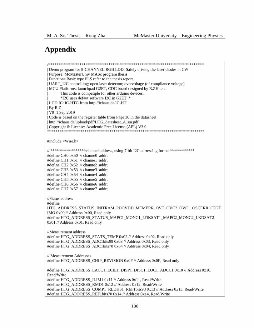
M. A. Sc. Thesis – Rong Zha McMaster University – Engineering Physics
136
Appendix
/***************************************************************************
| Demo program for 8-CHANNEL RGB LDD: Safely driving the laser diodes in CW
| Purpose: McMasterUniv MASc program thesis
| Functions:Basic type PLS refer to the thesis report
| UART_I2C controlling; open laser detecton; overvoltage (of compliance voltage)
| MCU Platforms: launchpad G2ET, CDC board designed by R.ZH, etc.
| This code is compatiple for other arduino devices.
| *I2C uses defaut software I2C in G2ET. *
| LDD IC: iC-HTG from http://ichaus.de/iC-HT
| By R.Z
| V0_1 Sep.2019
| Code is based on the register table from Page 30 in the datasheet
| http://ichaus.de/upload/pdf/HTG_datasheet_A1en.pdf
| Copyright & License: Academic Free License (AFL) V3.0
***************************************************************************/
#include <Wire.h>
// *****************channel address, using 7-bit I2C adrressing format************
#define CH0 0x50 // channe0 addr;
#define CH1 0x51 // channe1 addr;
#define CH2 0x52 // channe2 addr;
#define CH3 0x53 // channe3 addr;
#define CH4 0x54 // channe4 addr;
#define CH5 0x55 // channe5 addr;
#define CH6 0x56 // channe6 addr;
#define CH7 0x57 // channe7 addr;
//Status address
#define
HTG_ADDRESS_STATUS_INITRAM_PDOVDD_MEMERR_OVT_OVC2_OVC1_OSCERR_CFGT
IMO 0x00 // Address 0x00, Read only
#define HTG_ADDRESS_STATUS_MAPC1_MONC1_LDKSAT1_MAPC2_MONC2_LKDSAT2
0x01 // Address 0x01, Read only
//Measurement address
#define HTG_ADDRESS_STATS_TEMP 0x02 // Address 0x02, Read only
#define HTG_ADDRESS_ADC1bits98 0x03 // Address 0x03, Read only
#define HTG_ADDRESS_ADC1bits70 0x04 // Address 0x04, Read only
// Measurement Addresses
#define HTG_ADDRESS_CHIP_REVISION 0x0F // Address 0x0F, Read only
#define HTG_ADDRESS_EACC1_ECIE1_DISP1_DISC1_EOC1_ADCC1 0x10 // Address 0x10,
Read/Write
#define HTG_ADDRESS_ILIM1 0x11 // Address 0x11, Read/Write
#define HTG_ADDRESS_RMD1 0x12 // Address 0x12, Read/Write
#define HTG_ADDRESS_COMP1_RLDKS1_REF1bits98 0x13 // Address 0x13, Read/Write
#define HTG_ADDRESS_REF1bits70 0x14 // Address 0x14, Read/Write

M. A. Sc. Thesis – Rong Zha McMaster University – Engineering Physics
137
//CG gain and RDCO
#define HTG_CG_RDCO 0x15//Address 0x15, Read/Write
#define HTG_SOSCERR_SOVC_SOVT_MMONC_MOSCERR 0x16 //Address 0x16, Read/Write
//MODE address
#define HTG_ADDRESS_MODE 0x1C // Address 0x1C, Read/Write
/************* BIT definition***********************/
#define HTG_OPERATION_MODE 0x01 // Operation mode
#define HTG_CONFIG_MODE 0x02 // Config mode
#define HTG_EACC_APC_MODE 0x00 // APC mode
#define HTG_EACC_ACC_MODE 0x01 // ACC mod
#define HTG_DISC_ON 0x00 // EC enables channel
#define HTG_DISC_OFF 0x08 // EC does not enable channel
#define HTG_DISP_PLR_ON 0x00 // Programmable logarithmic monitor resistor for APC enabled
#define HTG_DISP_PLR_OFF 0x04 // Programmable logarithmic monitor resistor for APC disabled
#define HTG_EOC_OFFSET_COMP_OFF 0x00 // Regulator offset compensation disabled
#define HTG_EOC_OFFSET_COMP_ON 0x10 // Regulator offset compensation enabled
#define HTG_ADCC_ADC_OFF 0x00 // ADC disabled
#define HTG_ADCC_ADC_ON 0x02 // *ADC enabled
#define HTG_ADCC_ADC_SOURCE_VDD 0x00 // ADC sourced by V(VDD)
#define HTG_ADCC_ADC_SOURCE_VBL 0x20 // ADC sourced by V(VBL)
#define HTG_ADCC_ADC_SOURCE_VB 0x40 // ADC sourced by V(VB)
#define HTG_ADCC_ADC_SOURCE_MDL 0x60 // ADC sourced by V(MDL)
#define HTG_ADCC_ADC_SOURCE_MC 0x80 // ADC sourced by V(MC)
#define HTG_ADCC_ADC_SOURCE_VRN 0xA0 // ADC sourced by V(VRN)
#define HTG_ADCC_ADC_SOURCE_VRP 0xC0 // ADC sourced by V(VRP)
#define HTG_ADCC_ADC_SOURCE_ANIN 0xE0 // ADC sourced by V(ANIN)
#define HTG_REFbits98_00 0x00 // Reference bits 9:8, 00
#define HTG_REFbits98_01 0x01 // Reference bits 9:8, 01
#define HTG_REFbits98_10 0x02 // Reference bits 9:8, 10
#define HTG_REFbits98_11 0x03 // Reference bits 9:8, 11
#define HTG_MCVR 0x00 // MCx Voltage Range is 0 to 5V (0.55V datasheet error)
#define HTG_ENAM 0x00 // Analog modulation disabled
#define HTG_VRNHR 0x00 // unknown
#define HTG_NSW 0x40 // Standard regulation mode
#define HTG_EPNNP 0x00 // N-type laser
#define HTG_CG_2 0x00 // Channel current measurement gain: 2
#define HTG_CG_5 0x40 // Channel current measurement gain: 5
#define HTG_CG_10 0x80 // Channel current measurement gain: 10
#define HTG_CG_50 0xC0 // Channel current measurement gain: 50
#define HTG_RDCO_MIN 0x00 // Disable RDCO
#define HTG_RDCO_MAX 0x3F //
#define HTG_RMD_MIN 0x00 // Disable RMD
#define HTG_ILIM_DISABLE 0x00 // Overcurrent protection is disabled!!!!!
#define HTG_ILIM_MAX 0xFF // Maximum overcurrent threshold

M. A. Sc. Thesis – Rong Zha McMaster University – Engineering Physics
138
/*******RGB Channel parameters in standalone application is pre-known*********
| R 1.3A ILIM for 1.6A RMC 0.3 OHM1% Cg 2
| G 1.6A ILIM for 1.8A RMC 0.3 OHM1% Cg 2
| B 2.3A ILIM for 2.6A RMC 0.2 OHM1% Cg 2
| DPSSL 4.5A ILIM 5.5A RMC 0.1/0.08 OHM1% Cg 2************* special
| In order to achieve better accuracy, Calibration for DAC may be needed.
| Calculation based on I = (1.00235.^(N+1))/(10*Cg*RMC)--> N
*****************************************************************************/
//#define Red_Current 0x36A // 874
#define Red_Currentbits98 HTG_REFbits98_11
#define Red_Currentbits70 0x6A
//#define Green_Current 0x3C3 // 963
#define Green_Currentbits98 HTG_REFbits98_11
#define Green_Currentbits70 0xC3
//#define Blue_Current 0x3B0 // 944
#define Blue_Currentbits98 HTG_REFbits98_11
#define Blue_Currentbits70 0xB0
//#define DPSSL_Current 0x3A7 // 935
#define DPSSL_Currentbits98 HTG_REFbits98_11
#define DPSSL_Currentbits70 0xA7
/**********************Parameters for this project****************************/
//Overcurrent threshold for each channel by iC-HTG (OCP)
#define Red_Limit 0x94 // 138: 1-255 Limit*0.55/RMC/ A
#define Green_Limit 0xA7 // 167: 1-255: Limit*0.55/RMC/ A
#define Blue_Limit 0xF1 // 241: 1-255: Limit*0.55/RMC A
#define DPSSL_Limit HTG_ILIM_MAX // 255: 1-255: Limit*0.55/RMC A
// Open laser and current saturation detection by 10-bit ADC
#define Open_Laser_threshold_Vd_bits98 0x02 // Adjustment can be made
#define Open_Laser_threshold_Vd_bits70 0x50 // not care
#define Current_saturation_Vd_bits98 0x00 // Vd is smaller than 1V if the compliance volt for the
channel is 23V
#define Current_saturation_Vd_bits70 0x14
/************************** UART command defined in the thesis *************************/
//Enable a designated channel with the pre-setting
#define UART_En_Ldd_Ch0 0xA0
#define UART_En_Ldd_Ch1 0xA1
#define UART_En_Ldd_Ch2 0xA2
#define UART_En_Ldd_Ch3 0xA3
#define UART_En_Ldd_Ch4 0xA4
#define UART_En_Ldd_Ch5 0xA5
#define UART_En_Ldd_Ch6 0xA6
#define UART_En_Ldd_Ch7 0xA7
// Disable a designated channel
#define UART_Dis_Ldd_Ch0 0x50

M. A. Sc. Thesis – Rong Zha McMaster University – Engineering Physics
139
#define UART_Dis_Ldd_Ch1 0x51
#define UART_Dis_Ldd_Ch2 0x52
#define UART_Dis_Ldd_Ch3 0x53
#define UART_Dis_Ldd_Ch4 0x54
#define UART_Dis_Ldd_Ch5 0x55
#define UART_Dis_Ldd_Ch6 0x56
#define UART_Dis_Ldd_Ch7 0x57
// Modify the current for the designated channel
#define UART_Current_Ldd_Ch0 0xC0
#define UART_Current_Ldd_Ch1 0xC1
#define UART_Current_Ldd_Ch2 0xC2
#define UART_Current_Ldd_Ch3 0xC3
#define UART_Current_Ldd_Ch4 0xC4
#define UART_Current_Ldd_Ch5 0xC5
#define UART_Current_Ldd_Ch6 0xC6
#define UART_Current_Ldd_Ch7 0xC7
// Modify the current limit for the designated channel
#define UART_ILimit_Ldd_Ch0 0xB0
#define UART_ILimit_Ldd_Ch1 0xB1
#define UART_ILimit_Ldd_Ch2 0xB2
#define UART_ILimit_Ldd_Ch3 0xB3
#define UART_ILimit_Ldd_Ch4 0xB4
#define UART_ILimit_Ldd_Ch5 0xB5
#define UART_ILimit_Ldd_Ch6 0xB6
#define UART_ILimit_Ldd_Ch7 0xB7
//Request the RAM register from the designated channel
#define UART_RequestRam_Ldd_Ch0 0x60
#define UART_RequestRam_Ldd_Ch1 0x61
#define UART_RequestRam_Ldd_Ch2 0x62
#define UART_RequestRam_Ldd_Ch3 0x63
#define UART_RequestRam_Ldd_Ch4 0x64
#define UART_RequestRam_Ldd_Ch5 0x65
#define UART_RequestRam_Ldd_Ch6 0x66
#define UART_RequestRam_Ldd_Ch7 0x67
// Enable all the channels with pre-setting
#define UART_En_Ldd_All_Ch 0x25
// Disable all the channels
#define UART_Dis_Ldd_All_Ch 0x26
/********************************************************************************/
void HTG_SetConfigureMode(char channel);
void HTG_SetOperationMode(char channel);
bool Faulty_Open_Detect(char channel);// open laser detection
bool Faulty_Saturation_Detect(char channel); // over compliance voltage detection (or current saturation
detection)
void HTG_Channel_Init(char channel);
void HTG_Channel_Disable(char channel);
void Serial_I2C( );

M. A. Sc. Thesis – Rong Zha McMaster University – Engineering Physics
140
//bool open_relay();
void setup()
{
/************UART for developing new laser projector ************************************/
Serial.begin(9600, SERIAL_8E1); //UART as a slave; 9600bps with 8E1 format
/******** I2C alone can be used for standalone application
***************************************************/
Wire.begin(); // join i2c bus (address optional for master)
for (char i=CH6; i<=CH6; i++) // for (char i=CH5; i<=CH5; i++) set for debugging
{
// if(Faulty_Open_Detect(i))
// while(1); //latch all the channels
// else
{
HTG_Channel_Init(i);
}
}
}
void loop()
{
for (char i=CH6; i<=CH6; i++) // for (char i=CH5; i<=CH5; i++) set for debugging
{
// if(Faulty_Saturation_Detect(i))
// while(1); //latch all the channels, modification can be used to latch the channel in the open
connetion.
// else
{
Serial_I2C();
}
}
}
// *configuration mode "10"
void HTG_SetConfigureMode(char channel){
Wire.beginTransmission(channel); //
Wire.write(byte(HTG_ADDRESS_MODE)); // sets register pointer to the command register (0x1C)
Wire.write(HTG_CONFIG_MODE); //
Wire.endTransmission();
}
// *mode to "01"
void HTG_SetOperationMode(char channel){
Wire.beginTransmission(channel); //
Wire.write(byte(HTG_ADDRESS_MODE)); // sets register pointer to the command register (0x1C)

M. A. Sc. Thesis – Rong Zha McMaster University – Engineering Physics
141
Wire.write(HTG_OPERATION_MODE); //
Wire.endTransmission();
}
void HTG_Channel_Init(char channel){
byte HtgConfiguration;
HTG_SetConfigureMode(channel);
// *configure the laser channel
Wire.beginTransmission(channel); //
Wire.write(byte(HTG_ADDRESS_EACC1_ECIE1_DISP1_DISC1_EOC1_ADCC1)); // Write into
mutiple addresses in single I2C transmission with a starting reg address
switch (channel){
case CH0:break; // RESERVED
case CH1: // DPSSL WITH AN i6A240W DC/DC
HtgConfiguration = ( HTG_EACC_ACC_MODE | HTG_DISP_PLR_OFF | HTG_DISC_ON |
HTG_EOC_OFFSET_COMP_OFF | HTG_ADCC_ADC_ON|HTG_ADCC_ADC_SOURCE_ANIN );
Wire.write(HtgConfiguration);
HtgConfiguration = DPSSL_Limit;
Wire.write(HtgConfiguration);
HtgConfiguration = HTG_RMD_MIN; //RMD is not used
Wire.write(HtgConfiguration);
HtgConfiguration = (DPSSL_Currentbits98 | HTG_MCVR | HTG_ENAM | HTG_VRNHR |
HTG_NSW | HTG_EPNNP);
Wire.write(HtgConfiguration);
HtgConfiguration = DPSSL_Currentbits70;
Wire.write(HtgConfiguration);
HtgConfiguration = (HTG_CG_2 | HTG_RDCO_MIN);
Wire.write(HtgConfiguration);
break;
case CH2:break; // RESERVED
case CH3: // BLUE
HtgConfiguration = ( HTG_EACC_ACC_MODE | HTG_DISP_PLR_OFF | HTG_DISC_ON |
HTG_EOC_OFFSET_COMP_OFF | HTG_ADCC_ADC_ON|HTG_ADCC_ADC_SOURCE_ANIN ); //
Wire.write(HtgConfiguration);
HtgConfiguration = Blue_Limit;
Wire.write(HtgConfiguration);
HtgConfiguration = HTG_RMD_MIN; //RMD is not used
Wire.write(HtgConfiguration);
HtgConfiguration = (Blue_Currentbits98 | HTG_MCVR | HTG_ENAM | HTG_VRNHR |
HTG_NSW | HTG_EPNNP);
Wire.write(HtgConfiguration);
HtgConfiguration = Blue_Currentbits70;
Wire.write(HtgConfiguration);
HtgConfiguration = (HTG_CG_2 | HTG_RDCO_MIN);
Wire.write(HtgConfiguration);
break;
case CH4: // RED
HtgConfiguration = ( HTG_EACC_ACC_MODE | HTG_DISP_PLR_OFF | HTG_DISC_ON |
HTG_EOC_OFFSET_COMP_OFF | HTG_ADCC_ADC_ON|HTG_ADCC_ADC_SOURCE_ANIN );

M. A. Sc. Thesis – Rong Zha McMaster University – Engineering Physics
142
Wire.write(HtgConfiguration);
HtgConfiguration = Red_Limit;
Wire.write(HtgConfiguration);
HtgConfiguration = HTG_RMD_MIN; //RMD is not used
Wire.write(HtgConfiguration);
HtgConfiguration = (Red_Currentbits98 | HTG_MCVR | HTG_ENAM | HTG_VRNHR |
HTG_NSW | HTG_EPNNP);
Wire.write(HtgConfiguration);
HtgConfiguration = Red_Currentbits70;
Wire.write(HtgConfiguration);
HtgConfiguration = (HTG_CG_2 | HTG_RDCO_MIN);
Wire.write(HtgConfiguration);
break;
case CH5: // GREEN
HtgConfiguration = ( HTG_EACC_ACC_MODE | HTG_DISP_PLR_OFF | HTG_DISC_ON |
HTG_EOC_OFFSET_COMP_OFF | HTG_ADCC_ADC_ON|HTG_ADCC_ADC_SOURCE_ANIN );
Wire.write(HtgConfiguration);
HtgConfiguration = Green_Limit;
Wire.write(HtgConfiguration);
HtgConfiguration = HTG_RMD_MIN; //RMD is not used
Wire.write(HtgConfiguration);
HtgConfiguration = (Green_Currentbits98 | HTG_MCVR | HTG_ENAM | HTG_VRNHR |
HTG_NSW | HTG_EPNNP);
Wire.write(HtgConfiguration);
HtgConfiguration = Green_Currentbits70;
Wire.write(HtgConfiguration);
HtgConfiguration = (HTG_CG_2 | HTG_RDCO_MIN);
Wire.write(HtgConfiguration);
break;
case CH6: // GRRREN
HtgConfiguration = ( HTG_EACC_ACC_MODE | HTG_DISP_PLR_OFF | HTG_DISC_ON |
HTG_EOC_OFFSET_COMP_OFF | HTG_ADCC_ADC_ON|HTG_ADCC_ADC_SOURCE_ANIN );
Wire.write(HtgConfiguration);
HtgConfiguration = Green_Limit;
Wire.write(HtgConfiguration);
HtgConfiguration = HTG_RMD_MIN; //RMD is not used
Wire.write(HtgConfiguration);
HtgConfiguration = (Green_Currentbits98 | HTG_MCVR | HTG_ENAM | HTG_VRNHR |
HTG_NSW | HTG_EPNNP);
Wire.write(HtgConfiguration);
HtgConfiguration = Green_Currentbits70;
Wire.write(HtgConfiguration);
HtgConfiguration = (HTG_CG_2 | HTG_RDCO_MIN);
Wire.write(HtgConfiguration);
break;
case CH7: // RED
HtgConfiguration = ( HTG_EACC_ACC_MODE | HTG_DISP_PLR_OFF | HTG_DISC_ON |
HTG_EOC_OFFSET_COMP_OFF | HTG_ADCC_ADC_ON|HTG_ADCC_ADC_SOURCE_ANIN );
Wire.write(HtgConfiguration);
HtgConfiguration = Red_Limit;

M. A. Sc. Thesis – Rong Zha McMaster University – Engineering Physics
143
Wire.write(HtgConfiguration);
HtgConfiguration = HTG_RMD_MIN; //RMD is not used
Wire.write(HtgConfiguration);
HtgConfiguration = (Red_Currentbits98 | HTG_MCVR | HTG_ENAM | HTG_VRNHR |
HTG_NSW | HTG_EPNNP);
Wire.write(HtgConfiguration);
HtgConfiguration = Red_Currentbits70;
Wire.write(HtgConfiguration);
HtgConfiguration = (HTG_CG_2 | HTG_RDCO_MIN);
Wire.write(HtgConfiguration);
break;
default: //errro communication statement can be added
break;
}
Wire.endTransmission();
//*read back for the configuration: optional(code is not included here)
Wire.beginTransmission(channel); // Get the slave's attention, tell it we're sending a command byte
Wire.write(HTG_ADDRESS_STATUS_INITRAM_PDOVDD_MEMERR_OVT_OVC2_OVC1_OSCE
RR_CFGTIMO);//I2C points to STATUS0 register
Wire.endTransmission();
Wire.requestFrom(channel, 2); // Tell slave we need to read 2 bytes from the current register
if (2 <= Wire.available()) // if two bytes were received
{
Wire.read();
Wire.read();
}
HTG_SetOperationMode(channel);
}
bool Faulty_Open_Detect(char channel){
byte HtgConfiguration;
// reading back STATUS0&1 registers to pull up NCHK**Disable the crobar shunting path********
Wire.beginTransmission(channel); // Get the slave's attention, tell it we're sending a command byte
Wire.write(HTG_ADDRESS_STATUS_INITRAM_PDOVDD_MEMERR_OVT_OVC2_OVC1_OSCE
RR_CFGTIMO); //
Wire.endTransmission();
Wire.requestFrom(channel, 2); // Tell slave we need to read 1byte from the current register
if (2 <= Wire.available()) // if two bytes were received
{
Wire.read();
Wire.read();
}
//open relay (if there is a relay for ESD protection)
//enable 10bit ADC
Wire.beginTransmission(channel); //

M. A. Sc. Thesis – Rong Zha McMaster University – Engineering Physics
144
Wire.write(byte(HTG_ADDRESS_EACC1_ECIE1_DISP1_DISC1_EOC1_ADCC1)); //
HtgConfiguration = (HTG_ADCC_ADC_ON|HTG_ADCC_ADC_SOURCE_ANIN);
Wire.endTransmission();
//read back the voltage values from ANIN and VBL
Wire.beginTransmission(channel); // Get the slave's attention, tell it we're sending a command byte
Wire.write(HTG_ADDRESS_ADC1bits98); // 98 and 70 should read out in one transmission
Wire.endTransmission();
Wire.requestFrom(channel, 1); // Tell slave we need to read 1byte from the current register
if (1 <= Wire.available()) // if two bytes were received
{
if((Wire.read() & 0x03) >= Open_Laser_threshold_Vd_bits98)
return false;
else
return true;
}
return true; //defaut error for protection
}
bool Faulty_Saturation_Detect(char channel){
// Wire.beginTransmission(channel); //
// Wire.write(byte(HTG_ADDRESS_EACC1_ECIE1_DISP1_DISC1_EOC1_ADCC1));
// HtgConfiguration = (HTG_ADCC_ADC_ON|HTG_ADCC_ADC_SOURCE_ANIN);
// Wire.endTransmission();
//read back the voltage values from ANIN and VBL
Wire.beginTransmission(channel); // Get the slave's attention, tell it we're sending a command byte
Wire.write(HTG_ADDRESS_ADC1bits98); // 98 and 70 should read out in one transmission
Wire.endTransmission();
Wire.requestFrom(channel, 2); // Tell slave we need to read 1byte from the current register
if (2 <= Wire.available()) // if two bytes were received
{
if((Wire.read() & 0x03) == Current_saturation_Vd_bits98)
{
if(Wire.read() < Current_saturation_Vd_bits70)
return true;
}
else
return false;
}
return true; //default error for protecton
}
//Disable A designated LDD channel
void HTG_Channel_Disable(char channel){
byte HtgConfiguration;
HTG_SetConfigureMode(channel);
// *configure the laser channel
Wire.beginTransmission(channel); //
Wire.write(byte(HTG_ADDRESS_EACC1_ECIE1_DISP1_DISC1_EOC1_ADCC1)); // Write into
// multiple addresses in single I2C transmission with a starting reg address

M. A. Sc. Thesis – Rong Zha McMaster University – Engineering Physics
145
switch (channel){
case CH0:break; // RESERVED
case CH1: // DPSSL WITH AN i6A240W DC/DC
HtgConfiguration = HTG_DISC_OFF ;
Wire.write(HtgConfiguration);
break;
case CH2:break; // RESERVED
case CH3: // BLUE
HtgConfiguration = HTG_DISC_OFF ;
Wire.write(HtgConfiguration);
break;
case CH4: // RED
HtgConfiguration = HTG_DISC_OFF ;
Wire.write(HtgConfiguration);
break;
case CH5: // GREEN
HtgConfiguration = HTG_DISC_OFF ;
Wire.write(HtgConfiguration);
break;
case CH6: // GRRREN
HtgConfiguration = HTG_DISC_OFF ;
Wire.write(HtgConfiguration);
break;
case CH7: // RED
HtgConfiguration = HTG_DISC_OFF ;
Wire.write(HtgConfiguration);
break;
default: //errro communication statement can be added
break;
}
Wire.endTransmission();
//*read back for the configuration: optional(code is not included here)
Wire.beginTransmission(channel); // Get the slave's attention, tell it we're sending a command byte
Wire.write(HTG_ADDRESS_STATUS_INITRAM_PDOVDD_MEMERR_OVT_OVC2_OVC1_OSCE
RR_CFGTIMO);//I2C points to STATUS0 register
Wire.endTransmission();
Wire.requestFrom(channel, 2); // Tell slave we need to read 2 bytes from the current register
if (2 <= Wire.available()) // if two bytes were received
{
Wire.read();
Wire.read();
}

M. A. Sc. Thesis – Rong Zha McMaster University – Engineering Physics
146
HTG_SetOperationMode(channel);
}
void Serial_I2C( ){
byte HtgConfiguration_98;
byte HtgConfiguration_70;
if (Serial.available()){
switch(Serial.read()){
case UART_En_Ldd_Ch0: HTG_Channel_Init(CH0); break;
case UART_En_Ldd_Ch1: HTG_Channel_Init(CH1); break;
case UART_En_Ldd_Ch2: HTG_Channel_Init(CH2); break;
case UART_En_Ldd_Ch3: HTG_Channel_Init(CH3); break;
case UART_En_Ldd_Ch4: HTG_Channel_Init(CH4); break;
case UART_En_Ldd_Ch5: HTG_Channel_Init(CH5); break;
case UART_En_Ldd_Ch6: HTG_Channel_Init(CH6); break;
case UART_En_Ldd_Ch7: HTG_Channel_Init(CH7); break;
case UART_Dis_Ldd_Ch0: HTG_Channel_Disable(CH0); break;
case UART_Dis_Ldd_Ch1: HTG_Channel_Disable(CH1); break;
case UART_Dis_Ldd_Ch2: HTG_Channel_Disable(CH2); break;
case UART_Dis_Ldd_Ch3: HTG_Channel_Disable(CH3); break;
case UART_Dis_Ldd_Ch4: HTG_Channel_Disable(CH4); break;
case UART_Dis_Ldd_Ch5: HTG_Channel_Disable(CH5); break;
case UART_Dis_Ldd_Ch6: HTG_Channel_Disable(CH6); break;
case UART_Dis_Ldd_Ch7: HTG_Channel_Disable(CH7); break;
case UART_Current_Ldd_Ch0:
HtgConfiguration_98 = Serial.read() & 0x03; //Serial data bit10 and bit9;High byte first
HtgConfiguration_70 = Serial.read();
HTG_SetConfigureMode(CH0);
Wire.beginTransmission(CH0); //
Wire.write(HTG_ADDRESS_COMP1_RLDKS1_REF1bits98);
Wire.write(HtgConfiguration_98);
Wire.write(HtgConfiguration_70);
Wire.endTransmission();
HTG_SetOperationMode(CH0);break;
case UART_Current_Ldd_Ch1:
HtgConfiguration_98 = Serial.read() & 0x03; //Serial data bit10 and bit9;High byte first
HtgConfiguration_70 = Serial.read();
HTG_SetConfigureMode(CH1);
Wire.beginTransmission(CH1); //
Wire.write(HTG_ADDRESS_COMP1_RLDKS1_REF1bits98);
Wire.write(HtgConfiguration_98);
Wire.write(HtgConfiguration_70);
Wire.endTransmission();
HTG_SetOperationMode(CH1); break;
case UART_Current_Ldd_Ch2:
HtgConfiguration_98 = Serial.read() & 0x03; //Serial data bit10 and bit9;High byte first
HtgConfiguration_70 = Serial.read();
HTG_SetConfigureMode(CH2);
Wire.beginTransmission(CH2); //
Wire.write(HTG_ADDRESS_COMP1_RLDKS1_REF1bits98);
Wire.write(HtgConfiguration_98);

M. A. Sc. Thesis – Rong Zha McMaster University – Engineering Physics
147
Wire.write(HtgConfiguration_70);
Wire.endTransmission();
HTG_SetOperationMode(CH2); break;
case UART_Current_Ldd_Ch3:
HtgConfiguration_98 = Serial.read() & 0x03; //Serial data bit10 and bit9;High byte first
HtgConfiguration_70 = Serial.read();
HTG_SetConfigureMode(CH3);
Wire.beginTransmission(CH3); //
Wire.write(HTG_ADDRESS_COMP1_RLDKS1_REF1bits98);
Wire.write(HtgConfiguration_98);
Wire.write(HtgConfiguration_70);
Wire.endTransmission();
HTG_SetOperationMode(CH3); break;
case UART_Current_Ldd_Ch4:
HtgConfiguration_98 = Serial.read() & 0x03; //Serial data bit10 and bit9;High byte first
HtgConfiguration_70 = Serial.read();
HTG_SetConfigureMode(CH4);
Wire.beginTransmission(CH4); //
Wire.write(HTG_ADDRESS_COMP1_RLDKS1_REF1bits98);
Wire.write(HtgConfiguration_98);
Wire.write(HtgConfiguration_70);
Wire.endTransmission();
HTG_SetOperationMode(CH4); break;
case UART_Current_Ldd_Ch5:
HtgConfiguration_98 = Serial.read() & 0x03; //Serial data bit10 and bit9;High byte first
HtgConfiguration_70 = Serial.read();
HTG_SetConfigureMode(CH5);
Wire.beginTransmission(CH5); //
Wire.write(HTG_ADDRESS_COMP1_RLDKS1_REF1bits98);
Wire.write(HtgConfiguration_98);
Wire.write(HtgConfiguration_70);
Wire.endTransmission();
HTG_SetOperationMode(CH5); break;
case UART_Current_Ldd_Ch6:
HtgConfiguration_98 = Serial.read() & 0x03; //Serial data bit10 and bit9;High byte first
HtgConfiguration_70 = Serial.read();
HTG_SetConfigureMode(CH6);
Wire.beginTransmission(CH6); //
Wire.write(HTG_ADDRESS_COMP1_RLDKS1_REF1bits98);
Wire.write(HtgConfiguration_98);
Wire.write(HtgConfiguration_70);
Wire.endTransmission();
HTG_SetOperationMode(CH6); break;
case UART_Current_Ldd_Ch7:
HtgConfiguration_98 = Serial.read() & 0x03; //Serial data bit10 and bit9;High byte first
HtgConfiguration_70 = Serial.read();
HTG_SetConfigureMode(CH7);
Wire.beginTransmission(CH7); //
Wire.write(HTG_ADDRESS_COMP1_RLDKS1_REF1bits98);
Wire.write(HtgConfiguration_98);
Wire.write(HtgConfiguration_70);
Wire.endTransmission();
HTG_SetOperationMode(CH7); break;

M. A. Sc. Thesis – Rong Zha McMaster University – Engineering Physics
148
case UART_ILimit_Ldd_Ch0:
HtgConfiguration_70 = Serial.read();
HTG_SetConfigureMode(CH0);
Wire.beginTransmission(CH0);
Wire.write(HTG_ADDRESS_ILIM1);
Wire.write(HtgConfiguration_70);
Wire.endTransmission();
HTG_SetOperationMode(CH0); break;
case UART_ILimit_Ldd_Ch1:
HtgConfiguration_70 = Serial.read();
HTG_SetConfigureMode(CH1);
Wire.beginTransmission(CH1);
Wire.write(HTG_ADDRESS_ILIM1);
Wire.write(HtgConfiguration_70);
Wire.endTransmission();
HTG_SetOperationMode(CH1); break;
case UART_ILimit_Ldd_Ch2:
HtgConfiguration_70 = Serial.read();
HTG_SetConfigureMode(CH2);
Wire.beginTransmission(CH2);
Wire.write(HTG_ADDRESS_ILIM1);
Wire.write(HtgConfiguration_70);
Wire.endTransmission();
HTG_SetOperationMode(CH2); break;
case UART_ILimit_Ldd_Ch3:
HtgConfiguration_70 = Serial.read();
HTG_SetConfigureMode(CH3);
Wire.beginTransmission(CH3);
Wire.write(HTG_ADDRESS_ILIM1);
Wire.write(HtgConfiguration_70);
Wire.endTransmission();
HTG_SetOperationMode(CH3); break;
case UART_ILimit_Ldd_Ch4:
HtgConfiguration_70 = Serial.read();
HTG_SetConfigureMode(CH4);
Wire.beginTransmission(CH4);
Wire.write(HTG_ADDRESS_ILIM1);
Wire.write(HtgConfiguration_70);
Wire.endTransmission();
HTG_SetOperationMode(CH4); break;
case UART_ILimit_Ldd_Ch5:
HtgConfiguration_70 = Serial.read();
HTG_SetConfigureMode(CH5);
Wire.beginTransmission(CH5);
Wire.write(HTG_ADDRESS_ILIM1);
Wire.write(HtgConfiguration_70);
Wire.endTransmission();
HTG_SetOperationMode(CH5); break;
case UART_ILimit_Ldd_Ch6:
HtgConfiguration_70 = Serial.read();
HTG_SetConfigureMode(CH6);
Wire.beginTransmission(CH6);

M. A. Sc. Thesis – Rong Zha McMaster University – Engineering Physics
149
Wire.write(HTG_ADDRESS_ILIM1);
Wire.write(HtgConfiguration_70);
Wire.endTransmission();
HTG_SetOperationMode(CH6); break;
case UART_ILimit_Ldd_Ch7:
HtgConfiguration_70 = Serial.read();
HTG_SetConfigureMode(CH7);
Wire.beginTransmission(CH7);
Wire.write(HTG_ADDRESS_ILIM1);
Wire.write(HtgConfiguration_70);
Wire.endTransmission();
HTG_SetOperationMode(CH7); break;
case UART_RequestRam_Ldd_Ch0:
HtgConfiguration_70 = Serial.read();
Wire.beginTransmission(CH0);
Wire.write(HtgConfiguration_70);
Wire.endTransmission();
Wire.requestFrom(CH0,1);
Serial.write(Wire.read()); break; //send back to UART
case UART_RequestRam_Ldd_Ch1:
HtgConfiguration_70 = Serial.read();
Wire.beginTransmission(CH1);
Wire.write(HtgConfiguration_70);
Wire.endTransmission();
Wire.requestFrom(CH1,1);
Serial.write(Wire.read()); break; //send back to UART
case UART_RequestRam_Ldd_Ch2:
HtgConfiguration_70 = Serial.read();
Wire.beginTransmission(CH2);
Wire.write(HtgConfiguration_70);
Wire.endTransmission();
Wire.requestFrom(CH2,1);
Serial.write(Wire.read()); break; //send back to UART
case UART_RequestRam_Ldd_Ch3:
HtgConfiguration_70 = Serial.read();
Wire.beginTransmission(CH3);
Wire.write(HtgConfiguration_70);
Wire.endTransmission();
Wire.requestFrom(CH3,1);
Serial.write(Wire.read()); break; //send back to UART
case UART_RequestRam_Ldd_Ch4:
HtgConfiguration_70 = Serial.read();
Wire.beginTransmission(CH4);
Wire.write(HtgConfiguration_70);
Wire.endTransmission();
Wire.requestFrom(CH4,1);
Serial.write(Wire.read()); break; //send back to UART
case UART_RequestRam_Ldd_Ch5:
HtgConfiguration_70 = Serial.read();
Wire.beginTransmission(CH5);
Wire.write(HtgConfiguration_70);
Wire.endTransmission();

M. A. Sc. Thesis – Rong Zha McMaster University – Engineering Physics
150
Wire.requestFrom(CH5,1);
Serial.write( Wire.read()); break; //send back to UART
case UART_RequestRam_Ldd_Ch6:
HtgConfiguration_70 = Serial.read();
Wire.beginTransmission(CH6);
Wire.write(HtgConfiguration_70);
Wire.endTransmission();
Wire.requestFrom(CH6,1);
Serial.write(Wire.read()); break; //send back to UART
case UART_RequestRam_Ldd_Ch7:
HtgConfiguration_70 = Serial.read();
Wire.beginTransmission(CH7);
Wire.write(HtgConfiguration_70);
Wire.endTransmission();
Wire.requestFrom(CH7,1);
Serial.write(Wire.read()); break; //send back to UART
case UART_En_Ldd_All_Ch:
for (char i=CH0; i<=CH7; i++){
HTG_Channel_Init(i);
}
break;
case UART_Dis_Ldd_All_Ch:
for (char i=CH0; i<=CH7; i++){
HTG_Channel_Disable(i);
}
break;
default: break;
}
}
}