development of a software-defined radar › dtic › tr › fulltext › u2 › 1040116.pdf3....
TRANSCRIPT

ARL-TR-8152 ● OCT 2017
US Army Research Laboratory
Development of a Software-Defined Radar by Benjamin Kirk, Jonathan Owen, Kyle Gallagher, Anthony Martone, Kelly Sherbondy, Ram Narayanan, and
Shannon Blunt
Approved for public release; distribution is unlimited.

NOTICES
Disclaimers
The findings in this report are not to be construed as an official Department of the Army position unless so designated by other authorized documents. Citation of manufacturer’s or trade names does not constitute an official endorsement or approval of the use thereof. Destroy this report when it is no longer needed. Do not return it to the originator.

ARL-TR-8152 ● OCT 2017
US Army Research Laboratory
Development of a Software-Defined Radar
by Benjamin Kirk, Jonathan Owen, Kyle Gallagher, Anthony Martone, and Kelly Sherbondy Sensors and Electron Devices Directorate, ARL Ram Narayanan Pennsylvania State University, University Park, PA Shannon Blunt University of Kansas, Lawrence, KS Approved for public release; distribution is unlimited.
ii
REPORT DOCUMENTATION PAGE Form Approved OMB No. 0704-0188
Public reporting burden for this collection of information is estimated to average 1 hour per response, including the time for reviewing instructions, searching existing data sources, gathering and maintaining the data needed, and completing and reviewing the collection information. Send comments regarding this burden estimate or any other aspect of this collection of information, including suggestions for reducing the burden, to Department of Defense, Washington Headquarters Services, Directorate for Information Operations and Reports (0704-0188), 1215 Jefferson Davis Highway, Suite 1204, Arlington, VA 22202-4302. Respondents should be aware that notwithstanding any other provision of law, no person shall be subject to any penalty for failing to comply with a collection of information if it does not display a currently valid OMB control number. PLEASE DO NOT RETURN YOUR FORM TO THE ABOVE ADDRESS.
1. REPORT DATE (DD-MM-YYYY)
October 2017 2. REPORT TYPE
Technical Report 3. DATES COVERED (From - To)
29 May 2017–11 August 2017 4. TITLE AND SUBTITLE
Development of a Software-Defined Radar 5a. CONTRACT NUMBER
5b. GRANT NUMBER
5c. PROGRAM ELEMENT NUMBER
6. AUTHOR(S)
Benjamin Kirk, Jonathan Owen, Kyle Gallagher, Anthony Martone, Kelly Sherbondy, Ram Narayanan, and Shannon Blunt
5d. PROJECT NUMBER
5e. TASK NUMBER
5f. WORK UNIT NUMBER
7. PERFORMING ORGANIZATION NAME(S) AND ADDRESS(ES)
US Army Research Laboratory ATTN: RDRL-SER-U 2800 Powder Mill Road Adelphi, MD 20783-1138
8. PERFORMING ORGANIZATION REPORT NUMBER
ARL-TR-8152
9. SPONSORING/MONITORING AGENCY NAME(S) AND ADDRESS(ES)
10. SPONSOR/MONITOR'S ACRONYM(S)
11. SPONSOR/MONITOR'S REPORT NUMBER(S)
12. DISTRIBUTION/AVAILABILITY STATEMENT
Approved for public release; distribution is unlimited.
13. SUPPLEMENTARY NOTES
14. ABSTRACT
In wartime environments, radio frequency interference (RFI) is created by communication devices, jammers, and other electronic sources. The RFI spectrum is assumed to be nonstationary over time, which creates potential to disrupt desired radar operation. The cognitive radar system discussed herein mitigates the effects of RFI by sensing and adapting the transmitted waveform to the widest available (unoccupied) instantaneous bandwidth in real time. Consequently, the radar range resolution and target detection are ameliorated. Results of a prototype cognitive radar implemented on an Ettus X310 software-defined radio are presented.
15. SUBJECT TERMS
software-defined radio, SDR, cognitive radar, radio frequency interference, RFI, dynamic spectrum
16. SECURITY CLASSIFICATION OF: 17. LIMITATION OF ABSTRACT
UU
18. NUMBER OF PAGES
44
19a. NAME OF RESPONSIBLE PERSON
Benjamin Kirk a. REPORT
Unclassified b. ABSTRACT
Unclassified
c. THIS PAGE
Unclassified
19b. TELEPHONE NUMBER (Include area code)
(301) 394-1708 Standard Form 298 (Rev. 8/98)
Prescribed by ANSI Std. Z39.18

Approved for public release; distribution is unlimited. iii
Contents
List of Figures iv
List of Tables v
Acknowledgments vi
1. Introduction 1
2. Hardware 1
3. Software 3
4. Conclusions 8
5. Future Work 12
6. References 16
Appendix A. UBX-160 Isolation vs. Frequency 17
Appendix B. Software-Defined Radio Receiver Cascade Calculations 19
Appendix C. Spurious Free Dynamic Range (SFDR) Test Setup 23
Appendix D. Phase Coherent Radar Virtual Instruments (VI) 27
List of Symbols, Abbreviations, and Acronyms 33
Distribution List 35

Approved for public release; distribution is unlimited. iv
List of Figures
Fig. 1 PPS vs. I/O trigger rise times for phase coherent operations ............... 3
Fig. 2 LabVIEW virtual interface for control of SDR and processing received data .................................................................................................... 4
Fig. 3 DC offset removal subVI implemented in LabVIEW .......................... 5
Fig. 4 Range profile subVI implemented in LabVIEW ................................. 6
Fig. 5 Producer–consumer loop example ...................................................... 7
Fig. 6 Full transmission bandwidth achieved using 2 160-MHz chirp waveforms.......................................................................................... 8
Fig. 7 Testbed for cognitive radar demonstration .......................................... 9
Fig. 8 Received pseudorandom RFI ............................................................ 10
Fig. 9 Radar operation over a 160-MHz instantaneous bandwidth with interference ...................................................................................... 10
Fig. 10 Radar operation using optimal instantaneous transmission bandwidth ......................................................................................................... 11
Fig. 11 Range profiles calculated from matched filter while transmitting chirp waveforms over the full transmission bandwidth (red) or the optimized bandwidth (blue) .............................................................................. 12
Fig. 12 FPGA VI loop that ensures data are written to the BRAM address in a timed sequence and only executes when the user wants to change the output waveform .............................................................................. 13
Fig. 13 Second-loop stage of the FPGA VI that reads data from the BRAM and writes them to a FIFO buffer before outputting the waveform .... 14
Fig. 14 Second-loop stage of the FPGA VI that reads data from the BRAM and stores them in a FIFO buffer. The disabled code in the last step of the sequence is part of the debugging process. .................................. 14
Fig. 15 Transmit loop on the FPGA VI that reads the waveform from the FIFO buffer and outputs the samples. A state machine is used to transmit the waveform when it is available and output zeros if idle. ..................... 15
Fig. A-1 Isolation (dB) vs. frequency (MHz) for the RF front-end chain (UBX-160 daughterboards) of the universal software radio peripheral (USRP) X310 ................................................................................................ 18
Fig. B-1 Noise figure and gain calculations for the RF front-end chain (UBX-160 daughterboards) of the USRP X310 ........................................... 20
Fig. B-2 Cascaded noise figure, gain calculations, and saturation detection for the RF front end chain (UBX-160 daughterboards) of the USRP X310 ......................................................................................................... 21
Fig. C-1 Received intermodulation products for SFDR calculation ................. 24

Approved for public release; distribution is unlimited. v
Fig. C-2 SFDR measurement at center frequency 𝒇𝒇𝒇𝒇 = 𝟓𝟓𝟓𝟓 𝐌𝐌𝐌𝐌𝐌𝐌.................... 25
Fig. D-1 LabVIEW user interface for control of the software-defined radio (SDR) and processing received data. The left panel controls transceiver (Tx) and receiver (Rx) channel configuration. The middle panel selects the displayed data. The right panel controls various data monitoring operations. ...................................................................... 28
Fig. D-2 High-level block diagram of host virtual instrument for the phase coherent SDR system. All following figures describe specific operation details, including field-programmable gate array (FPGA) first-in, first-out (FIFO).. .................................................................. 28
Fig. D-3 Transmitter loop that includes logic for streaming the Tx waveform to the FPGA FIFO for transmission, loading parameters from the output of the spectrum sensing, multi-objective optimization (SS-MO) algorithm, and Tx channel waveform reconfiguration upon the user’s request.............................................................................................. 29
Fig. D-4 Producer loop that fetches received data from the universal software radio peripheral (USRP) FPGA and adds them to the processing queue that is initialized outside the loop. Logic is also included to reconfigure certain receiver parameters upon the user’s request........................... 29
Fig. D-5 Consumer loop for processing the acquired receiver data. Upper left: Loop reads an element from the queue, performs calibration corrections, and passes data into the main case statement that updates the display every 100 ms—saving resources on host computer. Bottom right: Main case statement can perform data-saving operations, instantiate the SS-MO algorithm based on the present received data, and plot processed data. Top right: Calculates a “flicker” rate caused by an unknown issue where blank data are received due to missed synchronization triggers or lack of available transmission data from stream failure. .................................................................................. 30
Fig. D-6 First half of the trigger loop: loop generates synchronized transmit and receive software triggers and writes them to the FPGA. Timer is user configurable. .................................................................................... 30
Fig. D-7 Second half of the trigger loop: this loop generates synchronized transmit and receive software triggers and writes them to the FPGA. Timer is user configurable. Last frame of the flat sequence writes a true and then false to create a “rising edge” for the FPGA to detect. . 31
List of Tables
Table 1 Gain, noise figure, and output power with input power Pin =−15 dBm and variable attenuation Pvar = −10 dB ........................... 3

Approved for public release; distribution is unlimited. vi
Acknowledgments
We would like to thank Dr Brian Phelan, Jacob Kovarskiy, and Dr Christopher Fazi for their support and mentorship.

Approved for public release; distribution is unlimited. 1
1. Introduction
The Ettus X310 software-defined radio (SDR) is a cheap alternative to creating custom radio systems for research and reconfigurable prototyping. Using National Instruments LabVIEW, software necessary for developing a cognitive radar prototype on the Ettus X310 SDR was developed. This technical report outlines the benefits and drawbacks of the SDR hardware and LabVIEW software control for prototype development.
The fundamental hardware limitations of the Ettus X310 and associated UBX-160 transceiver daughterboards are introduced. The developed LabVIEW functionalities for interfacing with the SDR hardware are specified, followed by a description of anticipated future work.
2. Hardware
The Ettus X310 in use is equipped with the following hardware1,2:
• Two 14-bit, 200-MS/s analog-to-digital converters
• Two 16-bit, 800-MS/s digital-to-analog converters
• XC7K410T field-programmable gate array (FPGA) containing 28 Mb of block random-access memory (BRAM)3
• 1 GB of dynamic RAM (DRAM)
• Two UBX-160 transceiver daughterboards
• 4 × peripheral component interconnect express (PCIe) and 10-Gb Ethernet communication interfaces
• GPS-disciplined oscillator (GPSDO)
• 15-pin, low-current, 3.3-V, auxiliary general purpose input/output (GPIO)
• 10-MHz reference clock input or output synchronization
• Pulse per second (PPS) trigger input and output (I/O) for firmware control
The SDR, which was populated with UBX-160 daughterboards, has a frequency range support of 50 MHz to 6 GHz. The raw stream rate of data, using the full transceiver duplex at maximum channel bandwidths, is 2.98 GB/s*. The current
* 200 MSPL/s per channel × 4 channels × 4 Bytes/SPL ÷ 230 = 2.98-GB/s stream rate

Approved for public release; distribution is unlimited. 2
state of software control only allows the use of 2 complex channels due to the data stream rate limitations of the PCIe interface†. The 10-Gb Ethernet interface is not currently supported for use with custom FPGA reconfiguration. Complex received data are streamed to the host computer for further processing. The size of each data block can be set according to user specifications.
Each UBX-160 transceiver daughterboard has one receiver (Rx) and one transceiver (Tx) port. The isolation between these ports with no cable connection varies between 25–60 dB depending on the frequency of operation. Each Rx channel has approximately 45 dB of image rejection during in-phase/quadrature (I/Q) demodulation. Isolation versus frequency is shown in Appendix A, Fig. A-1.
The SDR has an internal local oscillator (LO) phase noise of –90 dBc/Hz at a 1-kHz offset, or a frequency accuracy of 2.5 ppm. The GPSDO reduces the phase noise to –142 dBc/Hz at a 1-kHz offset. The GPSDO improves the frequency accuracy to 20 ppb, or 0.1 ppb if the GPS is synchronized with a GPS constellation.
The 15-pin auxiliary GPIO can read or write low-frequency square wave signals. The GPIO breakout could potentially be used to control multiple SDRs simultaneously from a master controller. The PPS trigger was originally programmed for synchronizing timestamps between multiple devices. By reconfiguring the internal FPGA, the PPS trigger is currently programmed to act as a square wave trigger with user-defined periodicity. A comparison of GPIO and PPS rise times for triggering a waveform output is shown in Fig. 1. The PPS trigger is superior to the GPIO for accurate triggering due to faster rise time and should be used for triggering other RF devices.
† 4 × PCIe, version 1.0 is limited to 2-GB/s stream rate (1 GB/s uplink and 1 GB/s downlink)

Approved for public release; distribution is unlimited. 3
Fig. 1 PPS vs. I/O trigger rise times for phase coherent operations
The SDR receiver hardware is configured according to the user-programmed center frequency. The following receiver frequency bands have different hardware chain configurations: 50–500 MHz, 500 MHz to 1.5 GHz, and 1.5–6 GHz. A programmable variable attenuator determines the total receiver gain, which can be varied between –6.5 and 21.2 dB. Theoretical values of gain and noise figure are listed in Table 1 for the receiver frequency bands with a constant input power of –15 dBm and of the variable attenuator set to 10 dB. Using component datasheets, the theoretical receiver operation values have been determined in a spreadsheet presented in Appendix B.
Table 1 Gain, noise figure, and output power with input power 𝐏𝐏𝐢𝐢𝐢𝐢 = −𝟏𝟏𝟓𝟓 𝐝𝐝𝐝𝐝𝐝𝐝 and variable attenuation 𝐏𝐏𝐯𝐯𝐯𝐯𝐯𝐯 = −𝟏𝟏𝟓𝟓 𝐝𝐝𝐝𝐝
Frequency band 50 MHz to 500 MHz
Frequency band 500 MHz to 1.5 GHz
Frequency band 1.5 GHz to 6 GHz
Total gain (dB) 15.0 23.6 20.2 Noise figure (dB) 13.3 5.0 7.9
The spurious free dynamic range (SFDR) of each receiver channel is between 79 dB and 86 dB across the frequency range of 50 MHz to 5.5 GHz. A description of the test setup for calculating SFDR is presented in Appendix C.
3. Software
A 2-channel phase coherent radar was developed by making modifications to the LabVIEW FPGA example virtual instruments (VI) screen-oriented text editor “USRP Simple Streaming with Time”.4 An overview of the radar utilities and

Approved for public release; distribution is unlimited. 4
current software limitations are presented in this section. The front panel of the host interface for the SDR is shown in Fig. 2. The interface displays transceiver channel configuration in the left pane, plots results in the center pane, and data control in the right pane. Figures describing the major components of the LabVIEW software are described in Appendix D.
Fig. 2 LabVIEW virtual interface for control of SDR and processing received data
Currently, only 2 complex transmission or reception channels can be used simultaneously due to data-processing rate limitations. Utilization of 1 transmission channel and 1 reception channel allows for phase coherent radar operation. Important features added to the LabVIEW FPGA template for phase coherent radar functionality are listed below. (A software description of each function is described in the remainder of this section.)
• Carrier cancellation
• Coherent averaging
• Range profile
• Power spectrum with calibrations
• Max/min hold
• I/Q data capture
• Producer-consumer loops

Approved for public release; distribution is unlimited. 5
• Sinusoid, sinc impulse, and chirp waveform transmission
• Transmitter channel reconfiguration on the fly
• Software-defined triggering signals
Due to LO phase interference with the RF signal carrier, a prominent LO leakage is found after frequency down-conversion at DC. To cancel out the DC carrier re-emergence, the mean complex value of the received data are subtracted from the complex data. Figure 3 demonstrates the block logic used to achieve DC cancellation of the received baseband data.
Fig. 3 DC offset removal subVI implemented in LabVIEW
The matched filter range profile is calculated in real time using fast Fourier transform (FFT) operations to perform a cross-correlation between the transmitted waveform and the received complex data. Figure 4 demonstrates the block logic used to achieve real-time range profile generation using an applied matched filter. The range profile is defined mathematically in terms of the transmitted signal s(f) and the received signal x(f) in Eq. 1:
𝑟𝑟(𝑡𝑡) = ℱ−1{ 𝑥𝑥(𝑓𝑓)𝑠𝑠(𝑓𝑓)∗} . (1)
The range profile is formed by performing the FFT of the transmitted and received signal, applying windowing in the frequency domain, conjugating the transmitted signal, performing a point-by-point multiplication of the 2 signals, and then computing the inverse FFT of the product. The output is converted from volts to dBV and is output on the bottom right wire. The 2 wires on the top right are used to generate an appropriate x-axis for the range profile plot.

Approved for public release; distribution is unlimited. 6
Fig. 4 Range profile subVI implemented in LabVIEW
The power spectra of received waveforms are calculated using an FFT with zero padding for precise frequency resolution. The received waveform power spectra are calibrated to the front ports of the SDR using given UBX-160 specifications and measurements made using a calibrated spectrum analyzer.5 Calibrations account for the variable attenuation. Maximum and minimum hold functions can be applied to the received power spectra. These hold functions are implemented by comparing the current spectrum plot, calculated from a received data block at time 𝑡𝑡1, to the subsequent received spectrum, calculated from a received data block at a later time 𝑡𝑡2. Each discrete frequency is then compared and the maximum or minimum power value at each frequency is maintained. Additionally, the complex received signal that is processed through LabVIEW may be saved to an external comma separated values (csv) file from the VI user interface.
Because multiple signal-processing operations are occurring continuously, producer–consumer loops are implemented to regulate processing traffic and allocate processing blocks to critical operations. The producer–consumer loops act as intermediary data buffers on the host computer.6 The producer loop instantiates host code to interface and acquire received data from the SDR. The acquired signal data are then sent from the producer loop to the consumer loop, which performs signal processing and displays data on the user interface. Without producer–consumer loops, received data may be lost or operations may become unsynchronized. The host computer’s operations must be computationally efficient so that the producer loop queue does not occupy the host memory. An indicator of the number of producer elements in queue exists in the data control pane of the user interface for analyzing host-side computational efficiency. An example of the standard structure for producer–consumer loops in LabVIEW is shown in Fig. 5.

Approved for public release; distribution is unlimited. 7
Fig. 5 Producer–consumer loop example
The updated transmitter software includes the ability to alternate between single tone, sinc pulse, and chirp waveform transmissions. Carrier frequency, bandwidth, and waveform sample resolution may be changed on the fly during radar operation. Transmitted waveforms may be time delayed by zero padding the beginning of the signal. Previous attempts to change the carrier frequency and sample rate of the receiver on the fly caused undesired effects and often required the SDR to be reset for proper reconfiguration.
The software-defined trigger is the most significant feature needed to realize a functional radar with transmitter and receiver channel synchronization. In the standard FPGA software template, continuous and finite modes of operation for the transmitter and receiver are available. The continuous mode triggers the receiver and transmitter to operate as fast as possible with no synchronization. The finite mode allows for the specification of a trigger source. Because no reliable trigger source is provided, the firmware of the PPS internal source was reconfigured to operate as a synchronization trigger (see hardware description). The host computer’s software is programmed to operate on a timed loop that controls a trigger signal that is sent to the PPS source and transceiver channels to synchronize processes. The frequency of the trigger source is specified by the user in the data control pane of the VI. The trigger time period is reconfigurable on the fly. If the trigger period becomes too small and the host computer cannot process data fast enough, then the data buffer will overflow and cause LabVIEW to crash. The indicator of the number of elements in the producer loop buffer should be monitored

Approved for public release; distribution is unlimited. 8
to ensure it is not increasing rapidly. Solutions to decrease the computational speed of the host computer will be investigated in the future.
Utilization of 2 transmission channels to achieve a maximum transmission bandwidth of 320 MHz is supported while no reception channels are in use. Two adjacent 160 MHz chirp waveforms are shown in Fig. 6. Each transmitter channel is capable of arbitrary waveform generation.
Fig. 6 Full transmission bandwidth achieved using 2 160-MHz chirp waveforms
4. Conclusions
The benefits of using cognitive radar are best demonstrated in terms of target detection capabilities. The test setup in Fig. 7 is used for demonstrating cognitive radar operations using the SDR and an Agilent M8190A arbitrary waveform generator (AWG). Green arrows denote a PCI express connection and blue lines indicate coaxial RF connections.

Approved for public release; distribution is unlimited. 9
Fig. 7 Testbed for cognitive radar demonstration
The transmitter in the SDR is capable of transmitting diverse waveforms, including chirp waveforms with a triggered pulse repetition interval. A transmitted chirp waveform was coupled into a delay line. The unterminated delay line emulates a point target at a distance equal to the length of the delay line divided by it is velocity factor. The reflection from the open-ended delay line was coupled into an RF signal combiner. To emulate a time-varying RF environment, an AWG was used to generate pseudorandom spectra. The spectra consist of randomly distributed sinusoids and chirp waveforms. The selection of percent occupancy and total energy of the pseudorandom spectra was influenced by data collected outdoors with a spectrum analyzer at Adelphi Laboratory Center in Adelphi, Maryland. The signal combiner was connected to the receive port of the SDR. An example spectrum of radio frequency interference (RFI) received on the SDR is displayed in Fig. 8.

Approved for public release; distribution is unlimited. 10
Fig. 8 Received pseudorandom RFI
Without a spectrum sensing algorithm, a standard radar system transmitting a chirp waveform may operate over the full 160 MHz of instantaneous bandwidth without considering RFI. Small radar targets would be difficult to identify due to the signal corruption caused by the RFI while operating over the full transceiver bandwidth. Radar operation over the full instantaneous bandwidth with interference is shown in Fig. 9.
Fig. 9 Radar operation over a 160-MHz instantaneous bandwidth with interference

Approved for public release; distribution is unlimited. 11
The cognitive radar implemented on the SDR operates using the spectrum sensing, multi-objective optimization (SS-MO) algorithm,7 which determines the widest unoccupied frequency band based on total energy and percent occupancy. The optimal bandwidth parameters from the SS-MO algorithm are used to update the occupied band of the transmitted waveform and avoid RFI. All devices are connected through a network-attached storage that is capable of communicating with all systems and storing collected data. Upon receiving the optimal band parameters from the SS-MO algorithm, the SDR is reconfigured to transmit within the desired instantaneous band. The reconfigured chirp waveform that is avoiding RFI is shown in Fig. 10.
Fig. 10 Radar operation using optimal instantaneous transmission bandwidth
By reconfiguring the transmitter operating band to an unoccupied frequency range, the target detection capability is significantly improved. Figure 11 displays the range profile determined from the given test setup transmitting a chirp waveform occupying the full transmission bandwidth and the optimal transmission bandwidth. The range profile determined using the full 160-MHz transmission bandwidth appears in red, while the range profile determined using the reconfigured optimum transmission is shown in blue. While operating over the full transmission bandwidth, the range profile has a relatively high noise floor due to RFI, which masks a small third target caused by reflections in the delay line. By reconfiguring the chirp waveform to operate in the optimal bandwidth, the range profile noise floor decreases significantly such that the third target can be easily detected. It is noted that by operating over a narrower bandwidth, the range resolution becomes

Approved for public release; distribution is unlimited. 12
coarser. Range resolution is related to waveform bandwidth, B, by Eq. 2. From this framework, the operation of the SS-MO algorithm in a cognitive radar system to improve target detection has been validated.
∆𝑅𝑅 ≈ 𝑐𝑐2𝐵𝐵
. (2)
Fig. 11 Range profiles calculated from matched filter while transmitting chirp waveforms over the full transmission bandwidth (red) or the optimized bandwidth (blue)
5. Future Work
Multiple updates to the current VI will be investigated in the future. The most desired functional improvement is to operate the transmitter channel outputs using the FPGA functions. This implementation would allow allocation of streaming rates for other purposes between the host computer and SDR. Other desirable implementations are to
• Operate post-processing operations on the FPGA.
• Create an operation mode for rapid acquisition of data with little data processing.
• Improve data rates by utilizing FPGA block RAM.
• Limit the number of transceiver samples with first-in, first-out (FIFO) sizes.
• Implement real-time cognitive radar operation.
Approved for public release; distribution is unlimited. 13
• Operate SSMO on FPGA using sequential operations.
• Investigate utilization of the 1-GB peripheral DDR3 RAM.
• Achieve nonlinear phase coherency between multiple channels.
• Improve multi-device time synchronization.
• Achieve wider bandwidths over time using frequency band stitching.
• Add further basic network analyzer capabilities.
• Reduce crosstalk between channels via hardware modifications.
• Improve consistency of triggered operations and real-time waveform reconfigurations.
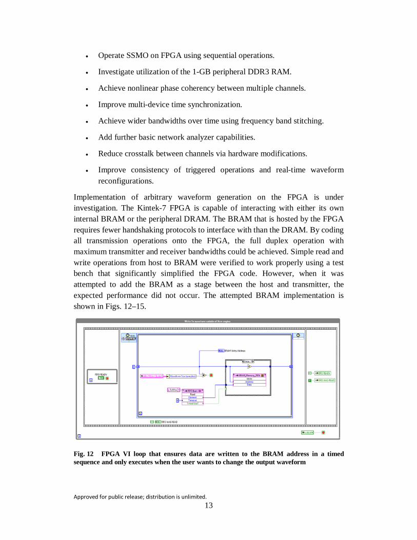
Implementation of arbitrary waveform generation on the FPGA is under investigation. The Kintek-7 FPGA is capable of interacting with either its own internal BRAM or the peripheral DRAM. The BRAM that is hosted by the FPGA requires fewer handshaking protocols to interface with than the DRAM. By coding all transmission operations onto the FPGA, the full duplex operation with maximum transmitter and receiver bandwidths could be achieved. Simple read and write operations from host to BRAM were verified to work properly using a test bench that significantly simplified the FPGA code. However, when it was attempted to add the BRAM as a stage between the host and transmitter, the expected performance did not occur. The attempted BRAM implementation is shown in Figs. 12–15.
Fig. 12 FPGA VI loop that ensures data are written to the BRAM address in a timed sequence and only executes when the user wants to change the output waveform

Approved for public release; distribution is unlimited. 14
Fig. 13 Second-loop stage of the FPGA VI that reads data from the BRAM and writes them to a FIFO buffer before outputting the waveform
Fig. 14 Second-loop stage of the FPGA VI that reads data from the BRAM and stores them in a FIFO buffer. The disabled code in the last step of the sequence is part of the debugging process.

Approved for public release; distribution is unlimited. 15
Fig. 15 Transmit loop on the FPGA VI that reads the waveform from the FIFO buffer and outputs the samples. A state machine is used to transmit the waveform when it is available and output zeros if idle.
The code in Fig. 15 is still under debugging and not operational. The buffer is necessary because the output clock uses an external data clock rather than the local FPGA system clock. This means that the transmit loop must wait for the waveform to be loaded into the buffer. Another reason for the buffer is that the BRAM has a single clock tick delay when reading data.

Approved for public release; distribution is unlimited. 16
6. References
1. Ettus Research. UBX USRP daughterboard system block diagram, UBX-160 datasheet. [accessed 2015 Mar] http://files.ettus.com/schematics/ubx/ubx.pdf.
2. Ettus Research. USRP hardware driver and USRP manual, USRP datasheet. [accessed 2016 May] http://files.ettus.com/.
3. Xillinx. Kintex-7 FPGAs, Kintex-7 FPGA datasheet. [accessed 2016 May] http://www.xilinx.com/support/documentation/selection-guides/kintex7-product-table.pdf.
4. Prototyping software-defined radio systems with LabVIEW FPGA hands-on seminar. From ni.com/training. 2014 July edition; Part No. 351260A-01. [accessed 2017 Sep]. ftp://ftp.ni.com/pub/events/seminar_elit/prototyping _software_defined_radio_systems_manual.pdf.
5. Ettus Research. RF characterization data UBX USRP daughterboard, UBX-160 datasheet. [accessed 2015 Feb]. http://files.ettus.com/ performance_data/ubx/UBX-without-UHD-corrections.pdf.
6. National Instruments. Application design patterns: producer/consumer. National Instruments; 2016 Aug 24. [accessed 2017 July]. http://www.ni.com/white-paper/3023/en/.
7. Martone A, Sherbondy K, Ranney K, Dogaru T. Passive sensing for adaptable radar bandwidth. Proceedings of the 2015 IEEE Radar Conference (RadarCon); 2015 May 10–15; Arlington (VA). IEEE; c2015. p. 0280–0285.
Approved for public release; distribution is unlimited. 17
Appendix A. UBX-160 Isolation vs. Frequency

Approved for public release; distribution is unlimited. 18
Fig. A-1 Isolation (dB) vs. frequency (MHz) for the RF front-end chain (UBX-160 daughterboards) of the universal software radio peripheral (USRP) X310

Approved for public release; distribution is unlimited. 19
Appendix B. Software-Defined Radio Receiver Cascade Calculations

Approved for public release; distribution is unlimited. 20
User inputs SFR Rx Input power (dBm): –15 Calculated values
Item Description Gain (dB)
NF (dB)
1dBCO (dBm)
Gain (1:1) NF(1:1)
1dBCI (dBm)
CBL Cable –0.5 0.5 300 0.891251 1.122018 300.5 SW1 AS236-321LF –1.3 1.3 32.7 0.74131 1.348963 34 A1 MGA-62563 20.4 1.4 17.7 109.6478 1.380384 –2.7 F1 LFCN-1700+ –0.97 0.97 300 0.799834 1.250259 300.97 SW2 SKY13350-385LF –0.8 0.8 24.2 0.831764 1.202264 25 AT1 HMC624ALP4e –10 10 20 0.1 10 30 SW3 SKY13350-385LF –0.8 0.8 24.2 0.831764 1.202264 25 AT2 N/A –1.5 1.5 300 0.707946 1.412538 301.5 F2 LFCN-2600+ –1.2 1.2 300 0.758578 1.318257 301.2 F3 LFCN-490+ –1.2 1.2 300 0.758578 1.318257 301.2 Mix1 LTC5510 3 13 14.6 1.995262 19.95262 11.6 AT3 N/A –1.5 1.5 300 0.707946 1.412538 301.5 F4 855916 –5 5 300 0.316228 3.162278 305 F5 LFCN-2600+ –1.2 1.2 300 0.758578 1.318257 301.2 SW4 SKY13350-385LF –0.8 0.8 24.2 0.831764 1.202264 25 A2 NBB-400 15.5 4.3 13 35.48134 2.691535 –2.5 AT4 N/A –1.5 1.5 300 0.707946 1.412538 301.5 TF1 TCM1-63AX+ –2.5 2.5 300 0.562341 1.778279 302.5 IQ_split ADL5380 6.9 10.9 16.9 4.897788 12.30269 10 NOTE: AT1 is variable (0 to –32 dB)
Fig. B-1 Noise figure and gain calculations for the RF front-end chain (UBX-160 daughterboards) of the USRP X310
Approved for public release; distribution is unlimited. 21
Cascaded values
Gain (1:1) NF(1:1) Gain
(dB) NF (dB)
Output Power (dBm)
Compressed? Generating Sig. Harmonics
NFDEG (dB)
0.891251 1.122018 –0.5 0.5 –15.5 NO NO 0.5 0.660693 1.513561 –1.8 1.8 –16.8 NO NO 1.3 72.4436 2.089296 18.6 3.2 3.6 NO NO 1.4 57.94287 2.092751 17.63 3.207175 2.63 NO NO 0.00717489 48.19478 2.096241 16.83 3.214413 1.83 NO NO 0.007238097 4.819478 2.282984 6.83 3.585028 –8.17 NO NO 0.370615006 4.008667 2.324952 6.03 3.664139 –8.97 NO NO 0.079111471 2.837919 2.427863 4.53 3.852242 –10.47 NO NO 0.188102587 2.152782 2.540008 3.33 4.04835 –11.67 NO NO 0.196108047 1.633052 2.687843 2.13 4.294038 –12.87 NO NO 0.245688359 3.258367 14.29349 5.13 11.55138 –9.87 NO NO 7.257344027 2.306747 14.4201 3.63 11.58968 –11.37 NO NO 0.038299505 0.729458 15.35747 –1.37 11.8632 –16.37 NO NO 0.273514331 0.55335 15.79376 –2.57 11.98486 –17.57 NO NO 0.121659247 0.460257 16.15929 –3.37 12.08422 –18.37 NO NO 0.099366611 16.33052 19.83449 12.13 12.97421 –2.87 NO NO 0.889987662 11.56112 19.85975 10.63 12.97974 –4.37 NO NO 0.005527775 6.501297 19.92707 8.13 12.99443 –6.87 NO NO 0.014696403 31.84198 21.6656 15.03 13.35771 0.03 NO NO 0.363272409
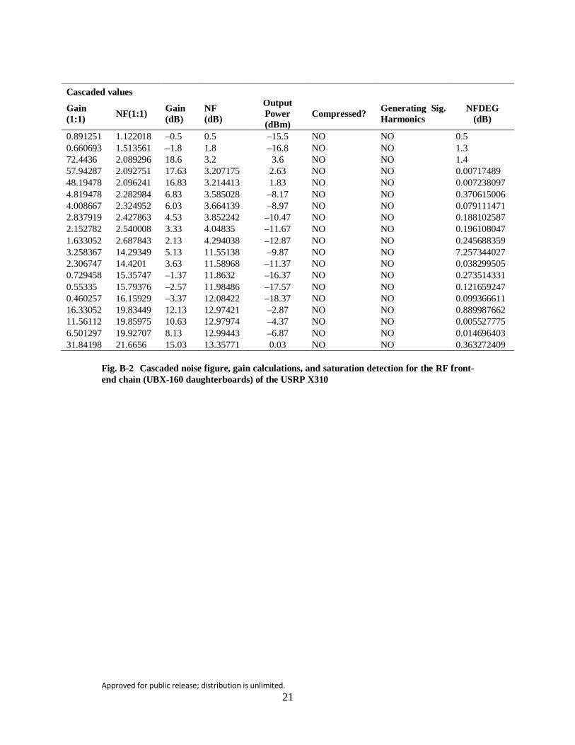
Fig. B-2 Cascaded noise figure, gain calculations, and saturation detection for the RF front-end chain (UBX-160 daughterboards) of the USRP X310

Approved for public release; distribution is unlimited. 22
INTENTIONALLY LEFT BLANK.

Approved for public release; distribution is unlimited. 23
Appendix C. Spurious Free Dynamic Range (SFDR) Test Setup

Approved for public release; distribution is unlimited. 24
Two isolated signal generators each generate a single tone. The tones are separated by 10 MHz in frequency and are merged using a high-isolation power combiner. The combined first-order tones are input to the front end of the software-defined radio (SDR) receiver.
After passing through the receiver chain, third-order intermodulation products are created by nonlinear components. The powers of the first-order input tones are compared to the powers of the nearby third-order intermodulation products. With a 1:1 increase of power for the 2 first-order tones, a 3:1 increase of power is expected for the 2 third-order harmonics when the input power is varied. A screen capture of the first-order and third-order tones is shown in Fig. C-1.
Fig. C-1 Received intermodulation products for SFDR calculation
The received first-order tone and third-order tone powers are plotted against the known input signal powers. A line of best fit is created for the first-order powers and for the third-order intermodulation powers. The SFDR is the difference in power between the first-order tones and third-order intermodulation products where the third-order line of best fit intercepts the noise floor (i.e., there are no detectable “spurs” generated by the receive chain for a given input power). One result is shown in Fig. C-2.
[dB]

Approved for public release; distribution is unlimited. 25
Fig. C-2 SFDR measurement at center frequency 𝒇𝒇𝒇𝒇 = 𝟓𝟓𝟓𝟓 𝐌𝐌𝐌𝐌𝐌𝐌

Approved for public release; distribution is unlimited. 26
INTENTIONALLY LEFT BLANK.
Approved for public release; distribution is unlimited. 27
Appendix D. Phase Coherent Radar Virtual Instruments (VI)

Approved for public release; distribution is unlimited. 28
Fig. D-1 LabVIEW user interface for control of the software-defined radio (SDR) and processing received data. The left panel controls transceiver (Tx) and receiver (Rx) channel configuration. The middle panel selects the displayed data. The right panel controls various data monitoring operations.
Fig. D-2 High-level block diagram of host virtual instrument for the phase coherent SDR system. All following figures describe specific operation details, including field-programmable gate array (FPGA) first-in, first-out (FIFO).

Approved for public release; distribution is unlimited. 29
Fig. D-3 Transmitter loop that includes logic for streaming the Tx waveform to the FPGA FIFO for transmission, loading parameters from the output of the spectrum sensing, multi-objective optimization (SS-MO) algorithm, and Tx channel waveform reconfiguration upon the user’s request
Fig. D-4 Producer loop that fetches received data from the universal software radio peripheral (USRP) FPGA and adds them to the processing queue that is initialized outside the loop. Logic is also included to reconfigure certain receiver parameters upon the user’s request.

Approved for public release; distribution is unlimited. 30
Fig. D-5 Consumer loop for processing the acquired receiver data. Upper left: Loop reads an element from the queue, performs calibration corrections, and passes data into the main case statement that updates the display every 100 ms—saving resources on host computer. Bottom right: Main case statement can perform data-saving operations, instantiate the SS-MO algorithm based on the present received data, and plot processed data. Top right: Calculates a “flicker” rate caused by an unknown issue where blank data are received due to missed synchronization triggers or lack of available transmission data from stream failure.
Fig. D-6 First half of the trigger loop: loop generates synchronized transmit and receive software triggers and writes them to the FPGA. Timer is user configurable.

Approved for public release; distribution is unlimited. 31
Fig. D-7 Second half of the trigger loop: loop generates synchronized transmit and receive software triggers and writes them to the FPGA. Timer is user configurable. Last frame of the flat sequence writes a true and then false to create a “rising edge” for the FPGA to detect.

Approved for public release; distribution is unlimited. 32
INTENTIONALLY LEFT BLANK.
Approved for public release; distribution is unlimited. 33
List of Symbols, Abbreviations, and Acronyms
AWG arbitrary waveform generator
BRAM block random-access memory
csv comma separated values
dBc/Hz decibels relative to the carrier/hertz
DC direct current
DRAM dynamic random-access memory
FFT fast Fourier transform
FIFO first-in, first-out
FPGA field-programmable gate array
GB gigabyte
Gb gigabit
GPIO general purpose input/output
GPS global positioning system
GPSDO GPS-disciplined oscillator
I/O input/output
I/Q in-phase/quadrature
LO local oscillator
MS/s mega samples per second
PCIe peripheral component interconnect express
ppb parts per billion
PPS pulse per second
RF radio frequency
RFI radio frequency interference
Rx receiver
SDR software-defined radio

Approved for public release; distribution is unlimited. 34
SFDR spurious free dynamic range
SS-MO spectrum sensing, multi-objective optimization
Tx transceiver
USRP universal software radio peripheral
VI virtual instruments
Approved for public release; distribution is unlimited. 35
1 DEFENSE TECHNICAL (PDF) INFORMATION CTR DTIC OCA 2 DIR ARL (PDF) RDRL DCM IMAL HRA RECORDS MGMT RDRL IRB TECH LIB 1 GOVT PRINTG OFC (PDF) A MALHOTRA 7 DIR ARL (PDF) RDRL SER U B KIRK J OWEN K GALLAGHER A MARTONE K SHERBONDY 2 PENNSYLVANIA STATE UNIVERSITY (PDF) R NARAYANAN UNIVERSITY OF KANSAS S BLUNT

Approved for public release; distribution is unlimited. 36
INTENTIONALLY LEFT BLANK.