development of bit-to-chip block for zigbee transmitter on fpga
DESCRIPTION
pTRANSCRIPT

Development of Bit-to-Chip Block for Zigbee Transmitter on FPGA
Rafidah Ahmad, Othman Sidek and Shukri Korakkottil Kunhi Mohd. Collaborative MicroElectronic Design Excellence Centre (CEDEC)
Universiti Sains Malaysia 14300 Nibong Tebal, Pulau Pinang, Malaysia
Abstract—Digital transmitter was developed on FPGA (Field Programmable Gate Array) in order to meet the needs for simple, low-power and low-cost wireless communication such as Zigbee. Zigbee operates primarily in the 2.4 GHz band, which makes the technology easily applicable and worldwide available. However, this paper only covers the bit-to-symbol block and the symbol-to-chip block of the digital transmitter for an acknowledgment frame. These two blocks are combined together as bit-to-chip block before implemented on Spartan3E XC3S500E FPGA. The purpose of the research is to diversify the design methods by using the Verilog code entry through Xilinx ISE 8.2i. Here, the simulation and measurement results are also presented to verify the functionality of the combined block. The frequency for input data and output data are 250 kHz and 2 MHz respectively.
Keywords-FPGA; Zigbee; bit-to-symbol; symbol-to-chip; Verilog
I. INTRODUCTION Zigbee is the name of the specification for short range
wireless communication that requires a low data rate, long battery life, low power consumption, secure networking, and cheaper technology. The Zigbee standard is also known as the IEEE 802.15.4 standard for Wireless Personal Area Networks (WPANs). The standard specifies that a compliant system will operate in three license-free bands: 2.45 GHz (250 kbps maximum data rate) for worldwide use, 868 MHz (20 kbps) for North America, and 915 MHz (40 kbps) for Europe [1]. The transmission range is 10 to 100 meters based on the environment [2].
The major applications of the Zigbee focus on sensor and automatic control such as military application, industrial control, smart buildings and environment monitoring [3]. The Zigbee architecture recognizes three devices: coordinator, router and end device [4]. Meanwhile, the Zigbee network layer supports three networking topologies: star, mesh, and cluster tree [5, 6]. There are four packet frame types: data, acknowledgment, MAC command and beacon [7].
In this paper, the design flow involving the behavioral coding, simulation and implementation of bit-to-symbol and symbol-to-chip blocks for Zigbee Standard on FPGA through Xilinx software is reported. The Spartan3E XC3S500E family has been used as FPGA device. This device is specifically designed to meet the needs of high volume and cost-sensitive consumer electronic applications. The device enhancements, combined with advanced 90 nm process technology, deliver more functionality and
bandwidth per dollar than was previously possible, setting new standards in the programmable logic industry [8].
This paper is organized as follows. In section II, an overview of the Zigbee digital transmitter is given including the characteristics of the bit-to-symbol and symbol-to-chip blocks. Section III explains the design methodology for each block. In section IV, the results and discussion of final simulation and measurement for the combined block is presented followed by the conclusion.
II. ZIGBEE TRANSMITTER Sixteen channels are available for the 2.4 GHz band
application with ample channel spacing of 5 MHz. This standard employs a DSSS (Direct Sequence Spread Spectrum) that uses a digital spreading function representing PN (Pseudo-random Noise) chip sequences [9].
As this project is focused on acknowledgment frame, it is used to confirm successful frame reception. Fig. 1 shows the structure of the acknowledgment frame based on [10], which originates from within the MAC sub-layer. This frame is constructed from an MHR (MAC Header) and an MFR (MAC Footer). The MHR contains the MAC Frame Control field and the DSN (Direct Sequence Number) while the MFR is composed of a 16-bit FCS (Frame Check Sequence). Together, the MHR and the MFR form the MAC acknowledgment frame and passes to the PHY as the PSDU (PHY Service Data Unit), which becomes the PHY payload. The PHY payload is prefixed with the SHR (Synchronization Header), containing the Preamble Sequence and the SFD (Start of Frame Delimiter) fields, and the PHR (PHY Header). The SHR, PHR and PHY payload form the PHY packet known as the PPDU (PHY Protocol Data Unit).
Figure 1. Schematic view of the acknowledgment frame and the PHY packet.
2009 Second International Conference on Computer and Electrical Engineering
978-0-7695-3925-6/09 $26.00 © 2009 IEEE
DOI 10.1109/ICCEE.2009.110
492
2009 Second International Conference on Computer and Electrical Engineering
978-0-7695-3925-6/09 $26.00 © 2009 IEEE
DOI 10.1109/ICCEE.2009.110
492
In this project, the Preamble Sequence contains 32 bits which are at logic ‘0’. For the SFD, the length is 8 bits with logic ‘1110 0101’ as stated in the Zigbee standard. The PHR also contains 8 bits in length with logic ‘1010 000’ [10]. The Frame Control is 16 bits in length with logic ‘0100 0100 0000 0000’. The Sequence Number logic is ‘1000 0000’. This gives the total of 88 bits for the acknowledgment frame.
Fig. 2 shows the block diagram of the proposed Zigbee digital transmitter based on [10] and [11]. Binary data from the PPDU packet is inserted into the CRC block and then to the bit-to-symbol block. After that, every 4 bits are mapped into one data symbol. The symbol-to-chip block performs the DSSS where each symbol is mapped into a 32-chip PN (Pseudo-random Noise) sequence [12]. In the 2.4 GHz band, the O-QPSK modulation is adopted. The fundamental O- QPSK method is to sum the in-phase signal with a quadrature phase signal delayed by half a cycle in order to avoid the sudden phase shift change [11]. Then, the modulated O-QPSK signal goes to the half-sine pulse shaping stage in order to reduce inter-symbol interference [13]. The resultant signal is transmitted by the RF (Radio Frequency) transmitter.
Figure 2. Detailed block diagram of the proposed Zigbee digital
transmitter.
A. Bit-to-symbol Block All the 88 bits from the CRC block is inserted into the
bit-to-symbol block. This binary information is mapped into the data symbol. The 4 LSBs (b0, b1, b2, b3) of each octet is mapped into one data symbol and the 4 MSBs (b4, b5, b6, b7) of each octet is mapped into the next data symbol. Each octet of PPDU is processed through the bit-to-symbol block sequentially, beginning with the Preamble field and ending with the last octet of the PSDU. For the final result, 22 symbols will be the output of the bit-to-symbol block.
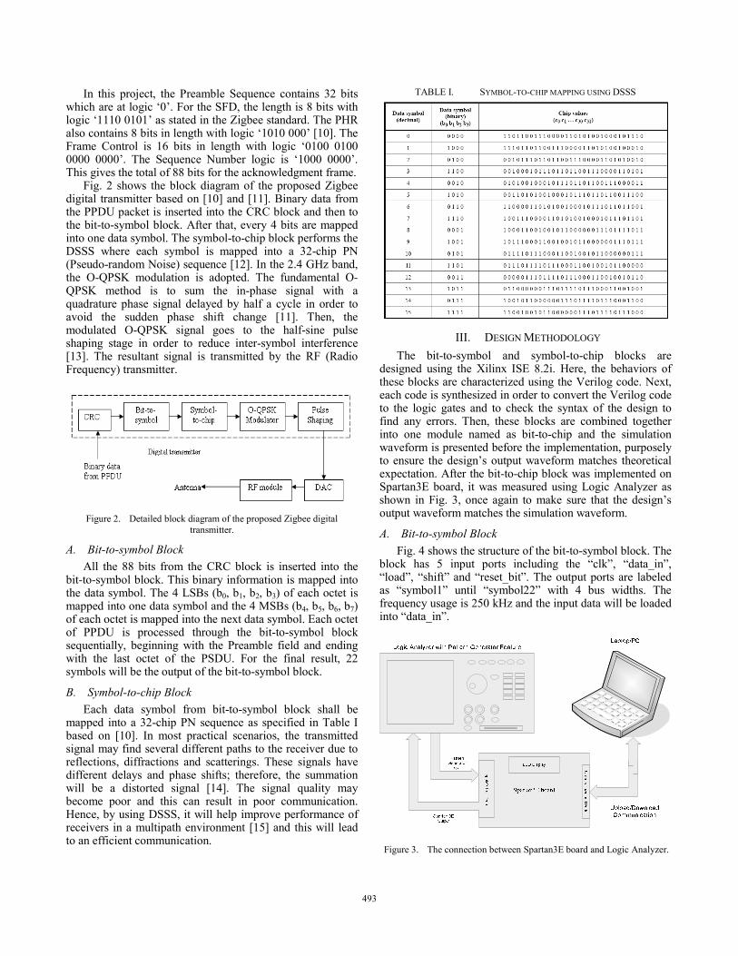
B. Symbol-to-chip Block Each data symbol from bit-to-symbol block shall be
mapped into a 32-chip PN sequence as specified in Table I based on [10]. In most practical scenarios, the transmitted signal may find several different paths to the receiver due to reflections, diffractions and scatterings. These signals have different delays and phase shifts; therefore, the summation will be a distorted signal [14]. The signal quality may become poor and this can result in poor communication. Hence, by using DSSS, it will help improve performance of receivers in a multipath environment [15] and this will lead to an efficient communication.
TABLE I. SYMBOL-TO-CHIP MAPPING USING DSSS
III. DESIGN METHODOLOGY The bit-to-symbol and symbol-to-chip blocks are
designed using the Xilinx ISE 8.2i. Here, the behaviors of these blocks are characterized using the Verilog code. Next, each code is synthesized in order to convert the Verilog code to the logic gates and to check the syntax of the design to find any errors. Then, these blocks are combined together into one module named as bit-to-chip and the simulation waveform is presented before the implementation, purposely to ensure the design’s output waveform matches theoretical expectation. After the bit-to-chip block was implemented on Spartan3E board, it was measured using Logic Analyzer as shown in Fig. 3, once again to make sure that the design’s output waveform matches the simulation waveform.
A. Bit-to-symbol Block Fig. 4 shows the structure of the bit-to-symbol block. The
block has 5 input ports including the “clk”, “data_in”, “load”, “shift” and “reset_bit”. The output ports are labeled as “symbol1” until “symbol22” with 4 bus widths. The frequency usage is 250 kHz and the input data will be loaded into “data_in”.
Figure 3. The connection between Spartan3E board and Logic Analyzer.
493493

Figure 4. The structure of the bit-to-symbol block.
The methodology of designing the bit-to-symbol block is summarized in the flow diagram in Fig. 5. From the starting point, if “reset_bit” is at logic ‘1’, then all the registers in this block will be reset. Otherwise, if “load” is at logic ‘1’, the data from “count_in” register will be loaded into “count_out” register. However, if the “load” is at logic ‘0’, then the process will depend on “shift” condition. If the “shift” is at logic ‘1’, the data from the “count_out” register will be stored in the “output” register. Otherwise, the data in the “output” register will always be at logic ‘0’. Finally, the data from this register will be divided and shifted to “symbol1” until “symbol22”. The Verilog code for the bit-to-symbol block will be synthesized and simulated in order to obtain the final result.
Figure 5. The design methodology of the bit-to-symbol block.
B. Symbol-to-chip Block As shown in Fig. 6, the symbol-to-chip block has 27
input ports: “symbol1_chip” until “symbol22_chip”,
“reload”, “reset_symbol”, “shift_symbol”, “clk1” and “clk2”; and “data_out” as the output port. The frequency for “clk1” and “clk2” are 250 kHz and 2 MHz, respectively.
Figure 6. The structure of the symbol-to-chip block.
The methodology of designing the symbol-to-chip block is shown in the flow diagram in Fig. 7. From the starting point, input data from “symbol_chip” will be shifted to a register labeled as “symbol_2” within “clk1”. Then, at “clk2”, when “reset_bit” is at logic ‘1’, then all the other registers in this block will be cleared. Otherwise, if “reload” is at logic ‘1’, each data symbol will be processed into a 32-chip PN sequence. However, if the “reload” is at logic ‘0’, then the process will depend on “shift_symbol” condition. If the “shift_symbol” is at logic ‘1’, the LSB (Least Significant Bit) of 32-chip will be shifted to “data_out” and this process is repeated until 704-chip. Otherwise, the “data_out” will always be at logic ‘0’. The Verilog code for the symbol-to-chip block will be synthesized, simulated and then downloaded together with the bit-to-symbol block onto FPGA to verify its functionality.
Figure 7. The design methodology of symbol-to-chip block.
494494

C. Bit-to-chip Block The bit-to-symbol and symbol-to-chip blocks are
combined together to form a bit-to-chip block, and then simulated and synthesized before implemented on Spartan3E XC3S500E as FPGA device. The structure of this block is shown in Fig. 8.
Figure 8. The structure of the bit-to-chip block.
IV. RESULTS AND DISCUSSION Final simulation was carried out for the bit-to-chip block
which was designed based on its characteristic. Then, the design code was implemented on Spartan3E as FPGA device in order to get the measurement result. All the input ports were forced to have certain logic based on the Zigbee Standard, and the output data was totally dependent on the input data. The frequency for “clk1” and “clk2” was set to 250 kHz and 2 MHz, respectively.
A. Simulation Waveform As shown in Fig. 9, when only “shift_symbol” is set to
logic ‘1’, the output data is shifted serially to the “data_out” from 415 250 ns until 767 250 ns. The total of the output chips are 704 within 352 000 ns.
Figure 9. Full view of simulation waveform for “data_out”.
For a detail comparison between simulation waveform and measurement waveform, Fig. 10 is captured. At 425 265 ns, the first and second chips of “data_out” are both at logic ‘1’, each within 500 ns. This is followed by the third chip with logic ‘0’.
From the final simulation waveform, it shows that the output data of the bit-to-chip block match the theoretical expectation. The timing for each input data is 4 μs and the output data is 500 ns.
Figure 10. Simulation waveform at the start of “data_out”.
B. Measurement Result From Fig. 11, it shows that when only “shift_symbol” is
enabled, the output data is shifted serially to the “data_out”. The range of “data_out” is approximately 352 002 ns and the logic is exactly similar to the output data in simulation waveform.
Figure 11. Full view of measurement waveform for “data_out”.
Fig. 12 shows that the first and second chips of
“data_out” are also both at logic ‘1’. Meanwhile, the third chip is at logic ‘0’. The timing for each chip is approximately 500 ns. This result shows that the logic of “data_out” for simulation and measurement are both identical.
Figure 12. Measurement waveform at the start of “data_out”.
From the measurement result, a small delay occurred at the “data_out” after the rising edge of a clock, which is most probably caused by pin and net delays on Spartan3E. Since the bit-to-chip block was implemented on Spartan3E with speed grade of 5, the following occupation was obtained: the configuration required about 967 slice flip flops of 9312 (10%). The LUTs usage is 1451 out of 9312 (15%). The average connection delay for this design is 1.317 ns. All signals were completely routed within 29 s with 182 MB
495495

CPU memory usage.
V. CONCLUSION This paper describes the development of the bit-to-chip
block as a part of the digital transmitter for 2.4 GHz band Zigbee Standard on FPGA. This block is used to improve the performance of receivers in a multipath environment. Verilog code has been used to characterize each bit-to-symbol and symbol-to-chip blocks behaviors which are then combined together to form the bit-to-chip block. This block is then simulated, synthesized and successfully downloaded on Spartan3E. From the measurement result, the functionality of the bit-to-chip block matches the theoretical expectation. The design has been verified with the frequency of 250 kHz and 2 MHz.
ACKNOWLEDGMENT The authors would like to acknowledge the Universiti
Sains Malaysia Short Term Grant for financial support of this project.
REFERENCES
[1] V. Adis. EDA 390-Computer Communication and Distributed Systems: A Paper on Zigbee. Available: http://www.cs.chalmers.se/~tsigas/Courses/DCDSeminar/Files/diovoad%20Zigbee.pdf .
[2] J. S. Lee, Y. W. Su and C. C. Shen, “A Comparative Study of Wireless Protocols: Bluetooth, UWB, Zigbee and WiFi,” in The 33rd Annual Conference of the IEEE Industrial Electronics Society (IECON), Taipei, Taiwan, Nov. 2007, pp. 46-51.
[3] Y. Zhou, X. Yang, X. Gou, M. Zhou and L. Wang, ”A Design of Greenhouse Monitoring & Control System Based on Zigbee Wireless Sensor Network,” in Proceedings of the International Conference on Wireless Communications, Networking & Mobile Computing, 2007, pp. 2563-2567.
[4] MSP430 Goes Zigbee/802.15.4. Available: http://focus.ti.com/lit/ml/slap129/slap129.pdf .
[5] C. C. William, “Zigbee: Wireless Control That Simply Works,” ZMD America, Inc.
[6] T. L. Khanh, “Zigbee System on Chip (SoC) Design,” High Frequency Electronics, pp. 16-25, January 2006.
[7] Introduction. Available: www.tutorial-reports.com/book/print/153 . [8] Xilinx, “Spartan3E FPGA Family: Complete Data Sheet”, 2006. [9] A. E. Oualkadi, L. V. Andendorpe and D. Flandre, “System-level
Analysis of O-QPSK Transceiver for 2.4 GHz band IEEE 802.15.4 Zigbee Standard,” 14th International Conference on Mixed Design, pp. 469-474, June 2007.
[10] IEEE 802.15.4-2003 Standard. Available: http://standards.ieee.org/getieee802/download/802.15.4-2003.pdf .
[11] C. C. Wang, J. M. Huang, L. H. Lee, S. H. Wang and C. P. Li. 2007. A Low Power 2.45 GHz Zigbee Transceiver for Wearable Personal Medical Devices in WPAN. Available: http://ieeexplore.ieee.org/iel5/4145986/4099325/04146217.pdf.
[12] ] S. Khaled, A. Maryam, B. Mohamed, J. Imad, S. Farag and L. Abderrahmane, “Performance Evaluation of IEEE 802.15.4: Experimental and Simulation Results,” Journal of Communications, Vol. 2, No. 4, pp. 29-37, June 2007.
[13] N. John, C. Anthony and L. Gary, “CMOS RFIC Architectures for IEEE 802.15.4 Networks,” Cadence Design Systems, Columbia, USA, 2003.
[14] W. C. Y. Lee, “Mobile Communication Engineering, Theory and Application,” 2nd ed., McGraw-Hill, NY, 1998.
[15] F. Shahin, “Zigbee Wireless Networks and Transceivers,” Newnes, USA,2008.
496496