development of gan-based blue leds and future · pdf filegan-based blue leds and future...
TRANSCRIPT
Development of GaN-based blue LEDsand future prospects
Monday June 8, 2015United Nations Educational, Scientific and Cultural Organization,
Paris
Hiroshi [email protected]
Professor, Graduate School of Engineering, Director, Akasaki Research Center,
Nagoya UniversityFuro-cho, Chikusa-ku, Nagoya, 464-8603, Japan 1/55
Acknowledgement:Professor Mohamed Sameh Amr, The Chairperson of the Executive Board of UNESCOMs. Irina Bokova, Director-General of UNESCOExcellencies, Distinguished delegates

To contribute to solving global issues such as,“Energy”, “Water”, “Food”, “Environment”,and “Health” and to realize sustainable society.
Our mission
2/55

Our group members
FacultyProf. Hiroshi AmanoAssoc. Prof. Yoshio HondaAssist. Prof. Deki Manato
Post Doctoral FellowKaddour LekhalSi-Young BaeKentaro NagamatsuAtsushi Tanaka
PhD. CandidatesMarc OlssonKohei YamashitaOh-Byung JungMaki KushimotoSeunga LeeSun ZhengHojun LeeBarry Ousmane 1
13 MC Students
5 Undergraduate Students
3 Secretaries
36 people
3/55

Post Doctoral Fellow
Dr. Kaddour Lekhal, AlegrilaPhD at Blaise Pascal University
World’s longest GaNnanowire
4/55

Device schematic of horizontal GaN NWs‐HEMT
Electronic Devices Light Emitting Diode (LED)
Waveguiding in 1D-nanostructures forMulti-Communication
AuNi
Sapphiresubstrate
NWs
AuNiNWs
50 µm
100 µm
200 µm3 µm
20 µm
3QWs InGaN/GaN
GaN wireLight at the ends of the NW
Laser illumination
Light at the bottom of the NW
Growth of High‐Aspect Ration GaN Nanowires
photonsSun
SUMITOMO Electric group
Solar Cells
Horizontal NWs
VLS growth
SAG growth
Self‐assembled growth

Post Doctoral Fellow
Dr. Si-Young Bae, Korea PhD at GIST
Ga-polar NR LEDs
1 μm
Pyramids
GaN nanowire LEDs6/55

PhD Candidate
Mr. Barry Ousmane 1 Guinea
Representative of Guinean students at the third International Conference on Quality Assurance in Higher Education in Africa and the capacity building workshop held respectively in Dakar and St. Louis (Senegal) by UNESCO Bamako Cluster Office in collaboration with partners in 2008.
7/55

8/55
Flame detector (UV light)www.directindustry.com
UV9 Security & Communications
UV astronomy-GALEX (courtesy NASA)
Back-illuminated AlGaN Schottky barrier diode (SBD)Back-illuminated UV-Visible light multi-band image sensor.
AlGaN‐PD array
Achievement as a MC student at TUT

History of blue LEDs
9/55

In this presentation, I would like to explain how “the seed” of blue light emitting diode, that is “Nitride Semiconductors”, have been developed and handed over by many researchers.
I also would like to show some perspective of the new development and applications of nitride-based light emitting devices.
10/55

http://www.gijyutu.com/kyouzai/mokei/ohki2/light.htmhttp://kagakukan.toshiba.co.jp/history/1goki/1940fluorescent.htmlhttp://www.pawanavi.com/topics/2002/11/06/http://www.audio-q.com/tyuumon.htm
~19C fire 1st generation
1878 incandescent lamp(Long history, Joseph Swan, UK, Thomas Edison, USA) 2nd generation
1938 Fluorescent lamp(Long history, 1901 Peter Cooper Hewitt, USA, 1927 Edmund Germer, 1938 Germany, George Innman, USA)3rd generation
1962 Commercial LED(Long history, Henry J. Round1907, Nick Holionyak Jr., USA)4th generation
Chemical reaction
Blackbody emission(early stage of quantum mechanics)
Energy transfer(Quantum mechanics)
Quantum mechanics based solid state lighting
History of artificial lighting
Luciaball, Dec.13, 2014 at Stockholm
11/55

Overview of development of LEDs
R. Haitz and J. Y. Tsao, phys. stat. sol. (a)208(2011)17
1962 N. Holonyak Jr., GaAsP red LD
1971 J. Pankove, GaN MIS blue LED
InGaN blue LED+ phosphor
Conventional III-V“The alloy road”
1952 H. Welker, GaAs, GaP
1968 RCA LCD
GaP:N Green
GaAsP:N Red-Orange-Yellow
12/55

GaN research in 1950’s -1970’s “Seed”
ZEITSCHRIFT FUR NATURFORSCHUNG A 14(1959)264.
J. Appl. Phys., 41(1970)4054.
Lund Institute of Technology or Lunds Tekniska Högskola (LTH)
H.G. Grimmeiss, H. Koelmans & I.B. Maak, German patent, DBP 1 077 330 (1960).
Dr. Grimmeiss at Lund University,Dec. 14, 2014 Aged 95
Professor Monemar at Lund University, Dec. 14, 2014
13/55

First GaN blue LED “Germination”
First GaN LED (MIS type)Efficiency : 10-5~3×10⁻⁴
J. I. Pankove, E. A. Miller, D. Richman and J. E. Berkeyheiser: J.Lumin. 4 (1971) 63.http://www.colorado.edu/memorybox/jacquespankove.htmlDr. Kayann Short • Farrand Academic Program, University of Colorado at Boulder • 303-492-1267 • [email protected]
14/55

GaN blue LED research in 1970’s “Endurance”
J. Electrochem. Soc., 123 (1978)1725.Hitachi
Y. Ohki, Y. Toyoda, H. Kobayashi and I. Akasaki, Intl. GaAs Symp., 479-484 (1981)
Matsushita Research Institute, Tokyo
(Panasonic)
Oki Electric
G. Jacob and D. Bois, Appl. Phys. Lett., 30 (1977) 412.
Philips
http://www.sslighting.net/lightimes/features/maruska_blue_led_history.pdf
Violet luminescence of Mg-doped GaNH. P. Maruska, D.A. Stevenson, J. I. PankoveAppl. Phys. Lett., 22, 303 (1973).
Stanford University and RCA
May 1981, New York
Mg
Mg
Zn
Zn
Zn
15/55

%.
.. 1627470
2747031850
Lattice mismatch
In general, lattice mismatchshould be <1%.
Why it was so difficult to grow high-quality GaN ?
GaN[0001]
(0001) C plane
[0001]
0.2747 nm0.3185 nm
Sapphire
Diamond 52,000 atm
1,200
GaN45,000 atm2,530
Bulk crystal Growth
Thin film growth
50 mJ. Karpinski and S. Porowski, JCG, 66(1984)1.
16/55

If I can achieveblue LEDs,
I will changethe world !
Braun tubes are too big !
Why I was interested in blue LEDs?
Isamu Akasaki1992- Meijo Univ.(Prof. Emeritus Nagoya Univ.)
1970 1990
1967 Vapour-grown AlNMatsushita Research Institute, Tokyo
1981Nagoya Univ.
1982 Undergraduate
Graduation Research “Nitride-Based Blue LED”
1975 Micro-soft by Bill Gates, Paul Allen 1976 Apple I by Steve Jobs, Stephen Wozniak
Doug Wilson/Corbis Melena, Joe
http://upload.wikimedia.org/wikipedia/commons/7/7e/Apple_II_IMG_4212.jpg
Apple IIPC-8001
http://www.mct.ne.jp/users/fjv/pc/pc8001.htm
I. Akasaki and M. HashimotoSolid State Commun. 5(1967)851.
1980 GaN LED by MBE and HVPE
17/55

GaCl + NH3 GaN + H2 + HCl
Heater850 ~1000
SiH2Cl2,H2
NH3,H2
Ga source Substrate
Exhaust
GaClHCl
Courtesy of Dr. Usui, Furukawa
• Multi zone temperature control • Bi-product NH4Cl• High growth rate >50 m/hr
S. A. Safvi et al., J. Electrochem. Soc., 144(1997)1789.
• Single temperature control
• Low growth rate ~ a few m/hr
HVPE: Halogen transport VPEMOVPE: Metalorganic VPE
Change of growth method from HVPE to MOVPE
HVPE MOVPE
18/55

Funding situation of our lab. in mid 80’s
Measuring susceptortemperature using pyrometer
1984
cf. Commercial MOVPE reactor ~1M US $
Lab-built MOVPE Reactor
0500
100015002000250030003500400045005000
1 2 3 4 5 6 7 8 9 10 11 12 13 14 15 16 17 18 19 20 21 22 23
10,0
00 J
PYen
1985 1990 1995 2000
1989・p
-Ga
N, p
nL
ED
Support by MEXT and JST 1985・L
T-
bu
ffer
Akasaki JST
Am100,000 US$
1984
Students built MOVPE reactor by themselves.
Y. Koide
19/55

High speed gas flow ~5 [m/s](conventional ~ 0.2[m/s])
H. Amano et al., Appl. Phys. Lett., 48(1986)353.
Reform of the MOVPE reactor by students
M. Hashimoto et al., J. Cryst, Growth, 68(1984)163.
20/55

Learn by trial and error
Random nucleation
Selective growth
Poor coalescence
I have tried more than 1,500 times, but I
could not grow high-quality GaN film.
21/55

Low-temperature-deposited buffer layer
I knew that the substrate temperature should be higher than1200 for the epitaxial growth of AlN.
Old oscillator did notwork well.
Temp.
Time
Deposition of AlN atlow temp.
~600
1,000
GaN growth
I rememberedthe discussion in
the lab.
February 1985
22/55
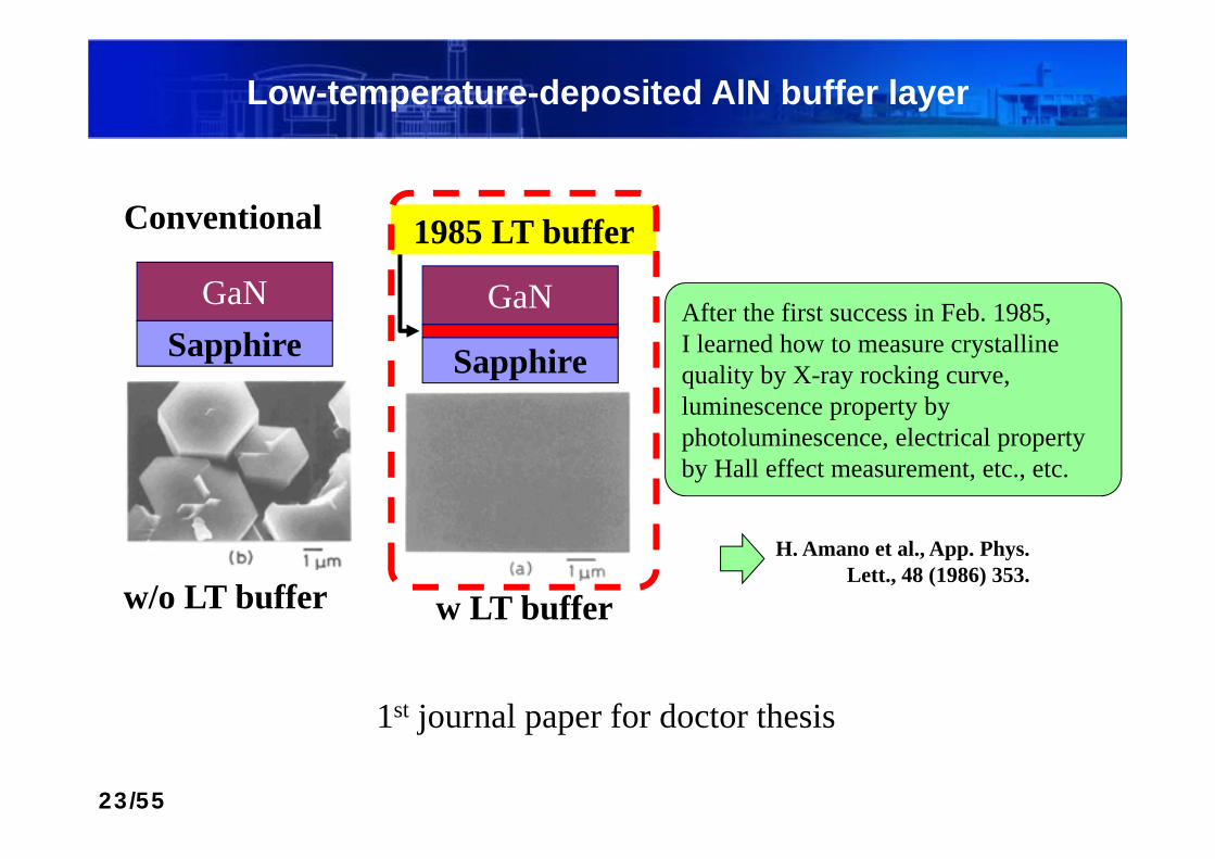
H. Amano et al., App. Phys. Lett., 48 (1986) 353.
Low-temperature-deposited AlN buffer layer
w/o LT buffer
Conventional
SapphireGaN
w LT buffer
Sapphire
GaN
1985 LT buffer
After the first success in Feb. 1985, I learned how to measure crystalline quality by X-ray rocking curve, luminescence property by photoluminescence, electrical property by Hall effect measurement, etc., etc.
23/55
1st journal paper for doctor thesis
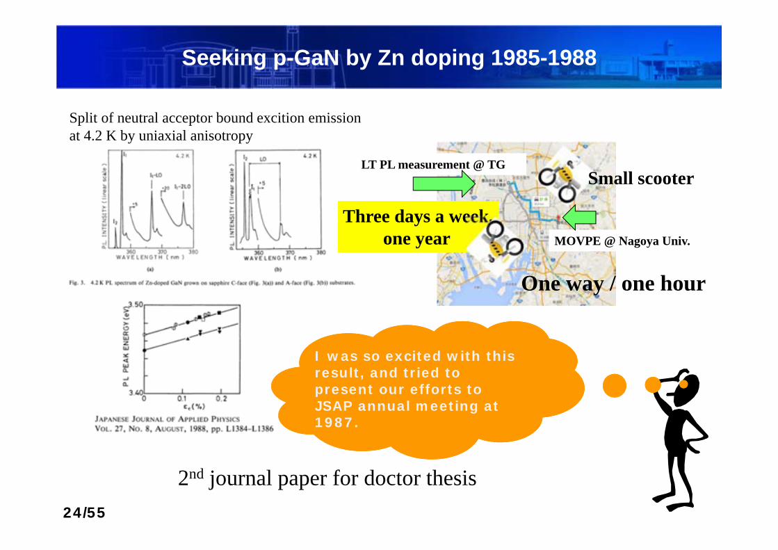
Seeking p-GaN by Zn doping 1985-1988
LT PL measurement @ TG
MOVPE @ Nagoya Univ.
I was so excited with this result, and tried to present our efforts to JSAP annual meeting at 1987.
Three days a week, one year
One way / one hour
Small scooter
Split of neutral acceptor bound excition emissionat 4.2 K by uniaxial anisotropy
24/55
2nd journal paper for doctor thesis
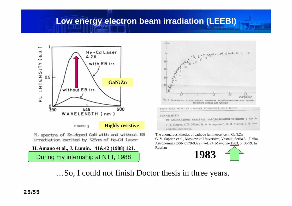
H. Amano et al., J. Lumin. 41&42 (1988) 121.
GaN:Zn
Highly resistive
Low energy electron beam irradiation (LEEBI)
During my internship at NTT, 1988
…So, I could not finish Doctor thesis in three years.
The anomalous kinetics of cathode luminescence in GaN:ZnG. V. Saparin et al., Moskovskii Universitet, Vestnik, Seriia 3 - Fizika, Astronomiia (ISSN 0579-9392), vol. 24, May-June 1983, p. 56-59. In Russian
1983
25/55

Selection of best dopant
Zn
MgJ. C. Phillips,“Bonds and Bands in Semiconductors”
Selection of the dopantActivation energy of acceptor in GaPZn : higher ×Mg: Lower ○
26/55

50m
H. Amano et al., Jpn. J. Appl. Phys. 28 (1989) L2112.
P-type GaN:Mg by LEEBI “Flowering”
(a) w LEEBI (b) wo LEEBI
M. Kito
27/55

Thermal annealing S. Nakamura et al, Jpn. J. Appl. Phys. 31 (1992) L139. Van Vechten et al., Jpn. J. Appl. Phys. 31 (1992) 3662.
J. Appl. Phys, 90(2001)108.
Thermal annealing and the mechanism
Hydrogen passivation
1992 Thermal annealingS. Nakamura et al., Jpn. J. Appl. Phys. 31(1992)1258.
28/55
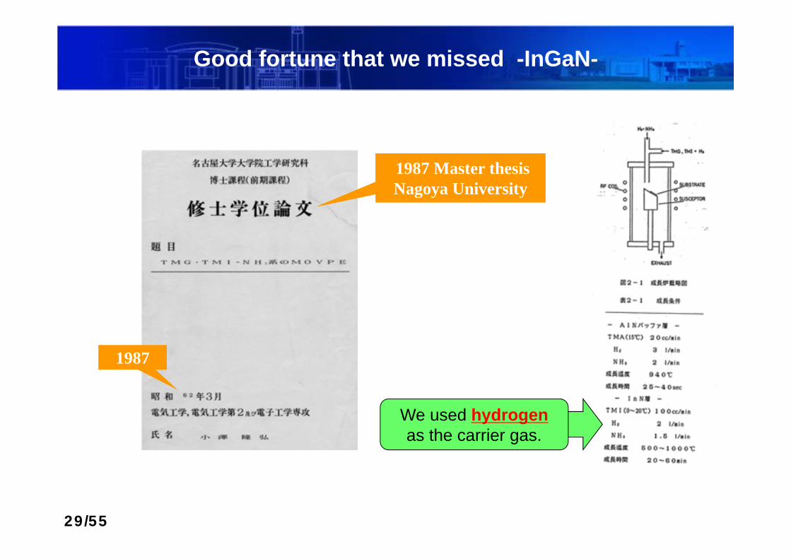
Good fortune that we missed -InGaN-
19871987
1987 Master thesisNagoya University 1987 Master thesisNagoya University
We used hydrogenas the carrier gas.
29/55

1989 International Conference on GaAs and Related Compounds
T. Matsuoka, *H. Tanaka, T. Sasaki and A. KatsuiNTT OPTO-ELECTRONICS LABORATPRIES Tokai, Ibaraki, 319-11 JAPAN
*NTT APPLIED ELECTRONICS LAABOTATORIES Musashino, Tokyo, 180 JAPAN
1989
Inst. Phys. Conf. Ser. No 106 : Chapter 3Paper Presented at Int. Symp. GaAs and Related Compounds, Karuizawa, Japan, 1989
Wide-gap semiconductor (In,Ga)N
They used nitrogenas the carrier gas.
30/55

N. Yoshimoto et al.,Appl. Phys. Lett., 59(1991)2251. S. Nakamura and T. Mukai
Jpn. J. Appl. Phys., 31(1992)L1457.
Blue luminescence at room temperature
31/55

S. Nakamura et al., Jpn. J. Appl. Phys.,32 (1993) L8.
1993 World’s first commercialization ofInGaN-based LEDs
World’s first commercialization “Fruition”
32/55
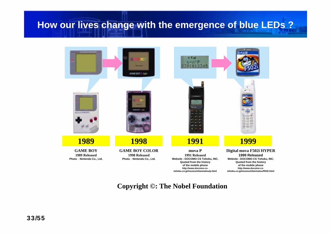
1989 1998 1991 1999mova P
1991 ReleasedWebsite : DOCOMO CS Tohoku, INC.
Quoted from the history of the mobile phonehttp://www.docomo-cs-
tohoku.co.jp/museum/tanmatsu/p.html
Digital mova F502i HYPER1999 Released
Website : DOCOMO CS Tohoku, INC.Quoted from the history
of the mobile phonehttp://www.docomo-cs-
tohoku.co.jp/museum/tanmatsu/f502i.html
GAME BOY1989 Released
Photo : Nintendo Co., Ltd.
GAME BOY COLOR1998 Released
Photo : Nintendo Co., Ltd.
Copyright ©: The Nobel Foundation
How our lives change with the emergence of blue LEDs ?
33/55
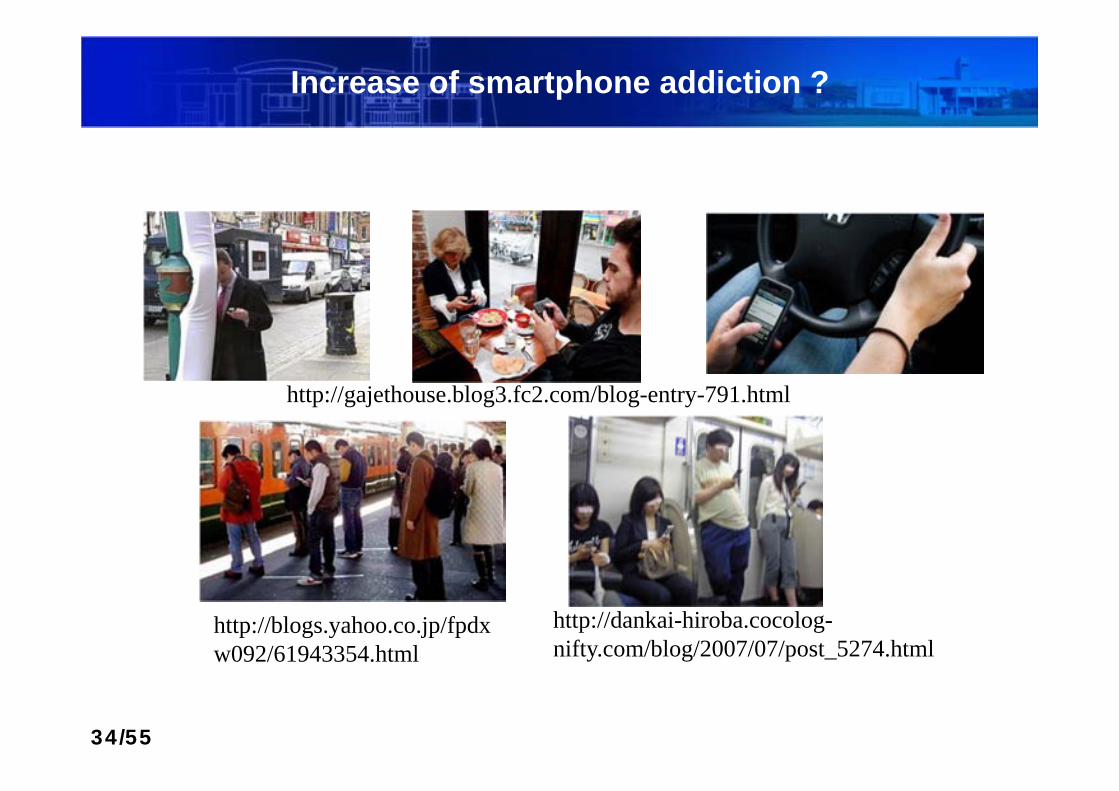
Increase of smartphone addiction ?
http://gajethouse.blog3.fc2.com/blog-entry-791.html
http://blogs.yahoo.co.jp/fpdxw092/61943354.html
http://dankai-hiroba.cocolog-nifty.com/blog/2007/07/post_5274.html
34/55

White LEDs “Contribution to society”
1996:White LED
Yellow PhosphorBlue LED
Wide-gap GaNBlue LED
Isamu Akasaki1967 Powdered AlN1981 Nagoya Univ.1992- Meijo Univ.(Prof. Emeritus Nagoya Univ.)
1985 LT buffer (MC, aged 24 )1989 P-type GaN (Research Associate, aged 28)
Hiroshi Amano1988 RA, Nagoya1989 Dr. of Eng., Nagoya Univ.1992-2010 Meijo Univ.2010 Nagoya Univ.
1987 JST1995 Commercialization
Toyoda Gosei
1989-1993:LT GaNp-type by thermal annealingInGaN/GaN DH
Shuji Nakamiura(Nichia, now UCSB)
Smartphone
©Gussisaurio
© Rotatebot
Three primary colorsNichia
Nichia
35/55
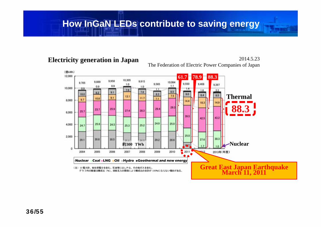
How InGaN LEDs contribute to saving energy
2014.5.23The Federation of Electric Power Companies of Japan
約300 TWh
Thermal
Nuclear
Electricity generation in Japan
88.3
Great East Japan Earthquake March 11, 2011
■Nuclear ■Coal ■LNG ■Oil ■Hydro ■Geothermal and new energy
61.7 78.9 88.3
36/55

U.S. DOE Energy Savings Potential of Solid-State Lighting in General Illumination Applications, Jan.2012
Total consumption4273 TWh
297/4273~7%
How InGaN LEDs contribute to saving energy
37/55

Year
LED lighting Other lighting LED ratio×1000
Data from Fuji Chimera Research Institute, Inc.,2014 LED Related Market Survey
In Japan, we can reduce total electricity consumption by about 7% (=1T JP Yen) by 2020.
Forecast of ratio of LED lighting in Japan
38/55

For the children living on Earth
Mr.Luvsannyam Gantumur, Minister for Education and Science of Mongolia
"Mongolia Ger" by Japanese Wikipedia
39/55

How long did it take from the first findings to contribute to mankind ?
科学技術振興機構(Japan Science and Technology Agency:JST)委託開発課題「窒化ガリウム(GaN)青色発光ダイオードの製造技術」(新技術の代表発明者:赤﨑勇 当時、名古屋大学教授)、開発実施企業:豊田合成株式会社) 1987年4月~1990年3月
http://www.jst.go.jp/itaku/result/ef-1.pdf
28 years from the start of JST support44 years from Pankove LED56 years from Grimmeiss paper
40/55

Challenge to DUV region for water purification
http://blogs.unicef.org/2014/03/20/world-water-day-2014-the-forgotten-768-million/
3 23 wwcubic caa
http://www.sei.co.jp/newsletter/2010/09/6a.html
Violet LDs for Blu-ray Disc
Blue LEDs, White LEDs
High frequency and high power HEMT
41/55

People who cannot access to safe water
UnicefWorld Health Organization,Progress on Drinking Water and Sanitation2014 Update
Drinking water coverage 2012
Sanitation facility coverage 2012
0.77 Billion people
2.6 Billion people
http://www.unicef.org/gambia/Progress_on_drinking_water_and_sanitation_2014_update.pdf42/55
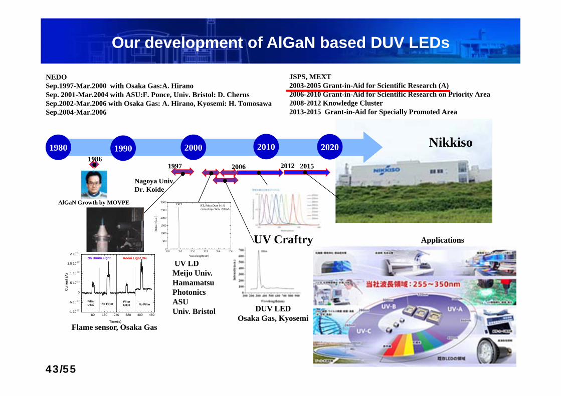
43/55
Nagoya Univ. Dr. Koide
Our development of AlGaN based DUV LEDs
-1 10-12
-5 10-13
0
5 10-13
1 10-12
1.5 10-12
2 10-12
80 160 240 320 400 480
Cur
rent
(A)
Time(s)
0229aMeij18-D Mesh electrodes
0V Flame response (d>4cm)
Room Light ONNo Room Light
No Filter No FilterFilterU330
FilterU330
1990 2000 2010 20201980
AlGaN Growth by MOVPE
Flame sensor, Osaka Gas
UV LDMeijo Univ.Hamamatsu Photonics ASUUniv. Bristol
350 351 352 353 354 3550
500
1000
1500
2000
2500
3000 350.9 RT, Pulse Duty 0.1% current injection: 200mA
Inte
nsity
[a.u
.]
Wavelength[nm]
DUV LEDOsaka Gas, Kyosemi
1997 2006 1986
UV Craftry Applications
2012 2015
Nikkiso
NEDOSep.1997-Mar.2000 with Osaka Gas:A. Hirano Sep. 2001-Mar.2004 with ASU:F. Ponce, Univ. Bristol: D. ChernsSep.2002-Mar.2006 with Osaka Gas: A. Hirano, Kyosemi: H. TomosawaSep.2004-Mar.2006
JSPS, MEXT 2003-2005 Grant-in-Aid for Scientific Research (A)2006-2010 Grant-in-Aid for Scientific Research on Priority Area2008-2012 Knowledge Cluster2013-2015 Grant-in-Aid for Specially Promoted Area

Our development of AlGaN based DUV LEDs
DUV-LED Sterilization DUV-LED array module
44/55

Other applications of group III nitrides
45/55

Why nitrides are so attractive for power device applications?
http://www.edn.com/Pdf/ViewPdf?contentItemId=4409627
GaAs
Si
GaN
46/55

Energy savings with GaN-based power devices
Highest efficiency power devices can be expected by usingGaN
En
erg
yL
oss
(10
0%
@Si
-IG
BT
)
0
20
40
60
80
100 ■Switching loss■Transmission loss
5% Loss ⇒0.75% Loss
Si 4H-SiC GaN (Materials)
Inverter(Si based IGBT)
Loss(Heat)5W
DC100W
AC95W
Role of Power Devices
• By replacing Si-based IGBT to WBG devices,9.8% of total electricity consumption can besaved.
• Super downsizing of power circuits is possible byusing GaN-based devices.
http://electronicdesign.com/power/optimize-power-scheme-these-transient-times47/55
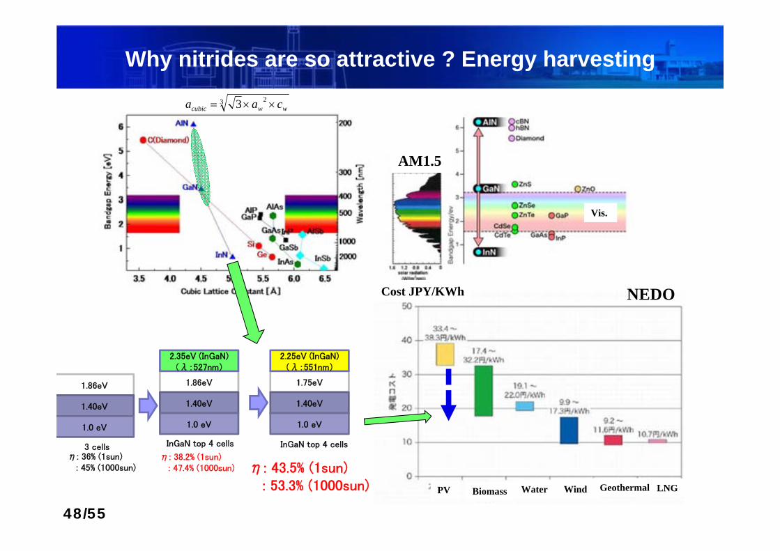
Why nitrides are so attractive ? Energy harvesting
1.86eV
1.40eV
1.0 eV
InGaN top 4 cells
η: 36% (1sun): 45% (1000sun)
1.86eV
1.40eV
1.0 eV
2.35eV (InGaN)(λ:527nm)
η: 38.2% (1sun): 47.4% (1000sun)
InGaN top 4 cells
1.75eV
1.40eV
1.0 eV
2.25eV (InGaN)(λ:551nm)
3 cells
η: 43.5% (1sun): 53.3% (1000sun)
NEDO
PV Biomass Water Wind Geothermal LNG
3 23 wwcubic caa
AM1.5
Vis.
Cost JPY/KWh
48/55

49/55
Achievements of our students

Laser on (001) Si
M. Kushimoto et al., Appl. Phys.Exp., 8 (2015) 022702.
Maki Kushimoto
Semi polar (1-101) GaN on (001) Si
• Chip to chip optical interconnection in Si LSI• Last one mile POF for low cost 4K and 8K TV
50/55
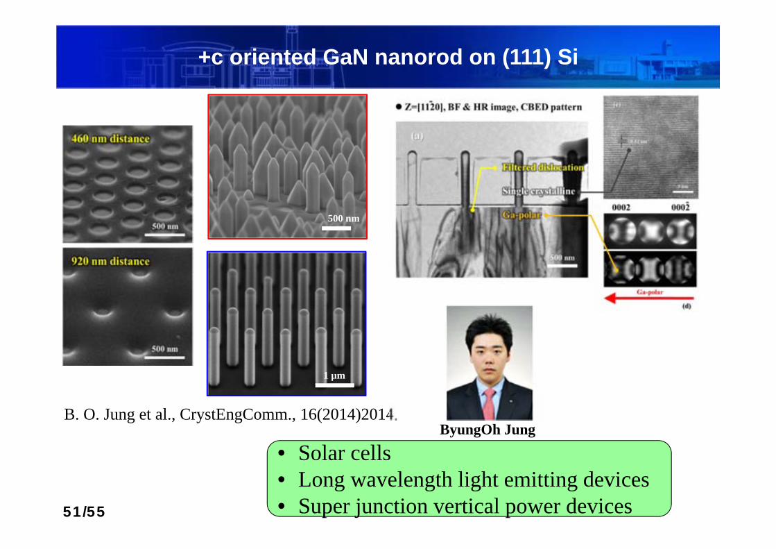
500 nm
1 µm
B. O. Jung et al., CrystEngComm., 16(2014)2014.ByungOh Jung
+c oriented GaN nanorod on (111) Si
• Solar cells• Long wavelength light emitting devices• Super junction vertical power devices51/55

Sun Zheng
Damage Layer Lattice Constant
The c-constant linearly increased with increasing the Mg concentration.
Damage Layer FWHM
HT-implan. (5×1019 cm-3 )
Damage Layer Intensity
-mode R.C. FWHM
P-type GaN by Mg ion implantation
52/55

Mechanical stack multi junction PV cell
1.86eV
1.40eV
1.0 eV
3接合上InGaN接合
VOC:3.0 VJSC:14 mA/cm2
η: 36% (1sun): 45% (1000sun)
1.86eV
1.40eV
1.0 eV
2.35eV (InGaN)(λ: ~527nm)
VOC: 4.63VJSC:9.54 mA/cm2
η: 38.2% (1sun): 47.4% (1000sun)
3接合上InGaN接合(第1・第2セルのEg変更)
1.75eV
1.40eV
1.0 eV
2.25eV (InGaN)(λ~551nm)
VOC: 4.44VJSC:11.15mA/cm2
η: 43.5% (1sun): 53.3% (1000sun)
格子不整合3接合
メカ
ニカ
ルス
タッ
ク
Mechanical Stack PV cellsSeunga Lee
In0.6Ga0.4N/In0.2Ga0.8N 100QWs
Voc(V) 1.57Jsc (mA/cm2) 31.56
CE (%) 29.82Fill factor (%) 90.48
Non polar simulation
Voc(V) 1.83Jsc (mA/cm2) 24.27
CE (%) 24.61Fill factor (%) 81.32
In0.6Ga0.4N/GaN 100QWs
53/55

54/55
My visit is supported by
Ministry of foreign affairs of Japan
ANA, an official partner of UNESCO

55/55
Acknowledgements
JSPS : Grant-in-Aid for Scientific Research “Specially Promoted Research”, #25000011
Special thanks to,Professors Isamu Akasaki, Nobuhiko Sawaki, Kazumasa Hiramatsu, MasafumiHashimoto, Satoshi Kamiyama, Tetsuya Takeuchi, Motoaki Iwaya, Masahito Yamaguchi (Passed away at 2013), Yoshio Honda, Nobuo Okazaki, Katsuhide Manabe, Koichi Ota, Naoki Shibata, Cyril Pernot, Akira Hirano, Masamichi Ipponmatsu, Hidemasa TomosawaMembers of Akasaki Laboratory, Nagoya University (1982-1992)Members of Akasaki and Amano Laboratory, Meijo University (1992-2010) Members of Amano, Yamagcuhi and Honda Laboratory (2010-)Toyoda Gosei, UVCR and Nikkiso Members
All the nitride researchers in the world !