development of improved techniques ... - universidade de vigo
TRANSCRIPT
Development of Improved Techniques for Design of UWB and
Multi-band Compact Planar Antennas and Filters with Performance
Enhancement
By: Azzeddin Naghar
Supervisors:
Ana Vázquez Alejos and Otman Aghzout
International Doctorate Mention
Academic Year: 2016/2017
Azz
eddi
n N
agha
r
Doc
tora
l Diss
erta
tion
2016
/201
7

International Doctoral School
Author: Azzeddin Naghar
Doctoral Dissertation
Development of Improved
Techniques for Design of UWB and
Multi-band Compact Planar Antennas
and Filters with Performance
Enhancement
Supervisors:
Ana Vázquez Alejos and Otman Aghzout
International Doctorate Mention
2016


International Doctoral School
Doctoral dissertation
Development of Improved Techniques for Design
of UWB and Multi-band Compact Planar Antennas
and Filters with Performance Enhancement
By: Azzeddin Naghar
Supervised by:
Ana Vázquez Alejos
Department of Signal Theory and Communications
Higher Technical School of Telecommunications Engineering
University of Vigo, Vigo, Spain
Otman Aghzout
Department of Telecommunications, National School of Applied
Science ENSATe
Abdelmalek Essaâdi University, Tetouan, Morocco
International Doctorate Mention
Academic Year: 2016/2017


Ana Vazquez Alejos, profesora titular de la Universidad de Vigo, Vigo, España,
en el Departamento de Teoría de señal y Comunicaciones
y
Otman Aghzout, profesor titular de la Universidad Abdelmalek Essaâdi,
Tetouan, Marruecos, en el Departamento de Telecomunicaciones, Escuela Nacional de
Ciencias Aplicadas
HACEN CONSTAR
Que la memoria titulada Development of Improved Techniques for Design of
UWB and Multi-band Compact Planar Antennas and Filters with Performance
Enhancement, ha sido realizada por D. Azzeddin Naghar bajo su dirección en el
Departamento de Teoría de señal y Comunicaciones de la Universidad de Vigo, y
constituye la Tesis por compendio de artículos que presenta para optar al grado de
International Doctor por la Universidad de Vigo.
Vigo, 2016/2017
Dr. D. Ana Vazquez Alejos Dr. D. Otman Aghzout
Director de la Tesis Director de la Tesis


To my mother, my father, my wife,
my brothers, my sister and my niece
To family and friends who believe in me

i
Abstract
Due to advancements in mobile radio communication technology intended to provide
high-data rates with frequency bandwidths not previously considered, there is an increase
in the demand of small size, low cost, multiband and high-performance ultra-wideband
antennas and filters. With a view to address these demands, this Thesis aims to propose
advanced antenna and filter design techniques leading to achieve excellent performance
devices applicable to multi-frequency and UWB systems. The set of techniques herein
described develops outstanding performance to meet the challenge of designing Multi-
Band/Ultra-Wideband (MB/UWB) bandpass filters and band-stop filters, as well as for
embedding the notch operation in UWB planar monopole antennas.
This Thesis starts with a block of content dedicated to investigating the parameters
involved in the process of designing parallel coupled line microstrip (PCLM) bandpass
filters. The first outcome is the development of a calculation tool that solves some
limitations presented by the commercial simulators available both in the market and in
the state of the art. This adhoc design tool facilitates the calculation of the optimal
parameters required to design N-order parallel coupled band pass filters with very low
cost of time and computational load and high accuracy in the performance checked by
experiment validation. The tool then facilitates an optimized filter design, and the main
feature is the ability to control the dimension of the gap space located between adjacent
resonators.
Based on this preliminary result, a further research step consisted of properly
setting a realistic or null spacing between adjacent coupled lines of the filter design
optimized by the design tool. This design technique attempts to solve manufacturing
problems by proposing a simple microstrip planar filter structure. By disregarding the gap
or sizing it to implementable values, it suppresses the influence of the imprecision
inherent to the microstrip planar manufacturing process. The design approach yields
highly efficient MB and UWB bandpass filters that demonstrates a good overall
performance with simple structure easy to manufacture. The control of the gap size offers
a good control of selected bands and in addition, it reduces the second harmonic response
for MB bandpass filters. Moreover, by incorporating other resonators like stubs or
metamaterial particles, we demonstrated an enhancement of selectivity and rejection for
designed MB and UWB bandpass filters.
ii
In a second part, this Thesis discusses the techniques investigated to obtain band
suppression feature in ultra-wideband (UWB) microstrip planar antenna designs that
prevents interference problems due to existing nearby communication systems within
UWB operating frequency. This second block of content starts presenting the design and
analysis of a dual band-notched monopole antenna, in which the method proposed to
obtain band-notched function consists of embedding two opposite U-shaped slots within
the radiating element. The key of innovation achieved with this method is the good control
of rejected narrow bands along with supplementary advantages of antenna small size, flat
frequency response and omnidirectional radiation pattern. Additionally, the applicability
of the developed techniques is considered and thereby it has been possible to analyze the
influence of the impairments introduced by the frequency dispersive propagation on the
UWB antenna design for body-based applications.
A second technique, valid to embed notching features in a microstrip UWB
antenna, consists of the use of single split ring resonator (SRR) placed on the backside of
the printed monopole to create the notch filtering function and thereby suppress the
interference problem. In this case, the capacitive coupling between the ground plane and
the loaded single SRR determines the properties of the band-stop filtering that widens the
impedance bandwidth and improves the rejection level of the antenna characteristics.
Furthermore, by etching a single SRR-slot in the radiating patch, the UWB antenna
exhibits dual-frequency notch performance without affecting the first rejected band.
Attained results of good omnidirectional pattern, acceptable and stable gain along with a
low profile make this antenna design idea a good candidate for UWB systems needed of
single- or multi-frequency notch filtering.
Keyword: RF filters, Antennas, UWB Systems, Multi-frequency, Notch Function, design
technique, Tool Calculation, Coupled lines, Numerical Validation, Experiment
Validation.
iii
Resumen
El desarrollo de tecnologías de comunicación inalámbrica con características de banda
ancha y alta velocidad de transmisión datos crece rápidamente, y para dichas tecnologías
la integración entre componentes se ha convertido en un tema muy importante. En
cualquier sistema de comunicaciones inalámbricas, la antena es un componente esencial
para recibir y transmitir señales, mientras que el filtro paso-banda (BPF) es otro
componente crucial para seleccionar señales en la banda requerida y rechazar las señales
no deseadas. La mayor parte de la investigación se ha centrado en la obtención de
componentes electrónicos y RF miniaturizados de baja potencia, aunque otros aspectos
relacionados con el diseño y la fabricación de antenas eficientes, miniaturizadas y
fácilmente integrables no han recibido la misma atención. Esta negligencia se extiende
también a las antenas y, en general, a todos los componentes de microondas distribuidos
pasivos, tales como resonadores, filtros y acopladores.
En términos de diseño de filtro, las características de operación de banda múltiple
(MB) y de banda ultra ancha (UWB) es un objetivo común para los sistemas de
comunicación inalámbrica actuales y, al mismo tiempo, lograr filtros paso-banda se ha
convertido en una exigencia para tales sistemas. Los requisitos impuestos al diseño de
estos circuitos obliga a afrontar nuevos retos entre los que se incluyen la obtención de un
buen rendimiento general, características de micro-paquete, de bajo coste y de uso fácil,
han sido el objetivo paralelo de la miniaturización de filtros paso-banda [1, 2]. Los filtros
paso-banda basados en líneas paralelas acopladas han sido ampliamente utilizados en
sistemas de microondas, debido a su buen rendimiento, estructura simple, bajo coste y
facilidad de integración con otros dispositivos [3, 4].
La estructura del filtro consiste en un conjunto de líneas microstrip de circuito
abierto acopladas. El espacio de acoplamiento o separación entre los resonadores
corresponde a los inversores de admitancia, en el circuito equivalente paso bajo. Las
impedancias características pares e impares de los resonadores de media onda acoplados
en paralelo se calculan usando inversores de admitancia. Estas impedancias de modo par
e impar se utilizan para calcular las dimensiones físicas del filtro, tal como se describe en
[5-7], ajustando adecuadamente las dimensiones del espacio de acoplamiento.
El objetivo principal de esta Tesis es el desarrollo de técnicas avanzadas
adecuadas para el diseño, la optimización, el ajuste fino y la realización práctica de filtros

iv
de microondas y antenas previstos con características de operación MB y de UWB.
Aunque la discusión en esta Tesis se centra solamente en dos tipos de componentes, filtros
y antenas, las técnicas desarrolladas pueden ser aplicadas a otros componentes resonantes
de microondas con las modificaciones convenientes.
Además de requerir filtros paso-banda MB y UWB operativos, la necesidad de
lograr una estructura de banco de filtros compacta ha impulsado el desarrollo de técnicas
de diseño para BPFs MB capaces de reducir la complejidad y el costo de los sistemas
front-end. En los circuitos planares, los filtros MB compactos pueden implementarse
usando diferentes enfoques básicos: mediante SIRs conectados a tierra por líneas
acopladas [8], resonadores de bucle abierto cargados con stubs [9], ranuras en el plano de
masa junto con stubs abiertos [10], o resonadores embebidos [11].
También es necesario considerar los requisitos estandarizados que se deben
cumplir en el diseño de un filtro paso-banda que cubra la banda de frecuencias UWB
definida por la Comisión Federal de Comunicaciones de Estados Unidos (FCC), que se
extiende de 3.1 a 10.6 GHz [12]. Entre estos requisitos podemos mencionar: cumplir con
la máscara de potencia impuesta al espectro UWB por la regulación FCC; bajas pérdidas
de inserción (<0.5 dB); bajo nivel de rizado en la banda de paso (<0.5 dB); variación
media del retardo de grupo (<0.2 ns); inserción de ceros de transmisión por encima y por
debajo de la banda de paso para alcanzar alta pendientes de atenuación fuera de banda [2,
13]. Se pueden encontrar en la literatura científica diversas aproximaciones para
implementar filtros UWB que cumplan estos requisitos regulatorios [14 - 16].
Otro factor que limita el diseño de filtros MB/UWB es la existencia de los
parásitos en la respuesta en frecuencia del filtro, principalmente debido a la presencia del
segundo armónico que emerge si se usan los diseños convencionales mencionados
anteriormente. Una respuesta en frecuencia con armónicos no deseados da lugar a una
característica de banda de paso asimétrica que degrada las propiedades de la banda
superior del filtro [17]. Recientemente, se han obtenido diversas técnicas [18 - 20] que
comparten la idea de modificar la estructura básica del filtro microstrip por algunos
medios, entre los que podemos mencionar: el uso de recubrimiento dieléctrico, inserción
de cortes en el plano de masa, uso de estructuras PBG, eliminación de sustrato, diseño de
ranuras periódicas, o el uso de técnicas de línea ondulada, y filtros que emplean formas
fractales.

v
Otro de los principales temas de interés de esta Tesis se refiere al diseño de antenas
UWB miniaturizadas que requieren integrar propiedades de filtrado de banda. Este
problema de diseño no es nuevo, y se convierte en uno de los principales factores que
afectan al progreso de la tecnología UWB. Como resultado, la literatura que aborda este
tema se ha extendido mucho en los últimos años [21- 24]. Las antenas UWB deben ser
eléctricamente pequeñas y económicas pero sin comprometer el rendimiento de la
operación. Un diagrama de radiación omnidireccional es preferible por ser adecuado para
redes ad hoc dotadas de orientación azimutal arbitraria impredecible. Sin embargo, sobre
la banda de frecuencias designada para UWB, existen algunas bandas estrechas que
correspondan a otros sistemas de comunicación, como WiMAX que opera en la banda de
3.3 a 3.7 GHz, WLAN que opera en la banda de 5.15 - 5.825 GHz, y la banda C que opera
a 7.2 GHz destinada a sistemas de comunicaciones satelitales. Estas comunicaciones de
banda estrecha pueden causar interferencia con un sistema UWB. Para solucionar este
problema es deseable diseñar antenas con integración de un filtro de rechazo de banda
centrado en estas bandas de frecuencia y capaz de minimizar una potencial interferencia.
Diferentes configuraciones encontradas en la literatura científica proponen el uso
de antenas impresas planas monopolo con elemento radiante y/o plano de masa
modificado, con el fin de lograr una característica de rechazo de bandas de frecuencia
[25-31]. Se puede obtener simple, doble o triple rechazo de banda de frecuencias
utilizando elementos parásitos [25, 26], insertando estructuras parásitas en forma de
varilla (rod-shaped) [27], utilizando un pequeño parche resonante [28], insertando una
ranura en la línea de alimentación, o bien integrando diferentes formas de ranuras tanto
en el parche de radiación como en el plano de masa [29-31]. Otros diseños incluyen
resonadores de anillo partido (SRR), o su estructura complementaria (CSRR), como
ranura conformada y/o conductor conformado, para producir la necesaria característica
de filtrado o eliminación de bandas de frecuencia [32-43].
Como se ha mencionado anteriormente, sobre la base de un filtro de tipo PCML,
la Tesis propone el diseño de filtros paso-banda MB y UWB mediante el ajuste del
espaciamiento entre resonadores acoplados con valor pequeño o nulo, como una técnica
para lograr la miniaturización del filtro. Además de las características MB y UWB, las
técnicas de diseño de filtros descritas en esta Tesis lograron minimizar los segundos
armónicos en la respuesta en frecuencia de los filtros MB, además de ofrecer un control
satisfactorio sobre la selección de la banda de frecuencia de operación requerida. Para el

vi
caso de los filtros UWB, se demostró por primera vez que estos requisitos de diseño
pueden lograrse considerando una separación nula entre todos los resonadores adyacentes
del filtro. Sin embargo, todavía era necesario resolver la limitación del diseño en términos
de rechazo de señal. En nuestro caso, incorporamos stubs en corto-circuito con el objetivo
de mejorar la selectividad del filtro y eliminar la transmisión a baja frecuencia. Por lo
demás, es posible mejorar todos los filtros propuestos en términos de selectividad,
rechazo en las frecuencias fuera de banda y supresión de espurios, añadiendo otros
resonadores como stubs o partículas metamateriales CSRR [44].
Después de haber alcanzado con éxito nuevas técnicas para diseño miniaturizado
de filtros, la investigación desarrollada en esta Tesis pudo abordar la integración de filtros
en el diseño de antenas UWB con el fin de proporcionar operación de rechazo de banda.
Como se ha mencionado anteriormente, una de las cuestiones clave en un sistema de
comunicación UWB es el diseño de una antena compacta que proporcione características
de banda ancha para cubrir toda la banda de operación UWB definida por el FCC. Debido
a sus atractivas propiedades de banda ancha, estructura simple y diagrama de radiación
omnidireccional, las antenas monopolo planas [45-47] se han utilizado como posibles
candidatos para aplicaciones UWB. Por lo tanto, en esta investigación se han considerado
como punto de partida el diseño y análisis de antenas UWB monopolo microstrip planas.
Se han realizado diferentes estudios sobre la integración de la función de filtrado notch
en dichas antenas.
En esta Tesis se han logrado diseños de antena con características de rechazo de
de una o dos o incluso múltiple banda de frecuencia. La primera de las técnicas propuestas
se basa en incluir una ranura en forma de U para lograr la supresión de radiación en la
banda a eliminar, mientras que en una segunda configuración propuesta se propone
colocar un único conductor parásito SRR en el plano de masa. En esta última
configuración, la operación de filtrado notch se debe al acoplamiento electromagnético
entre el parche y el conductor parásito. Ambas técnicas de rechazo de banda ofrecen
rechazos de banda estrechos o anchos y un control de las bandas rechazadas por medio
de un procedimiento de diseño simple. Las configuraciones propuestas han obtenido
beneficios adicionales, como un adecuado diagrama de radiación omnidireccional,
ganancia de antena estable, bajo perfil y bajo coste de fabricación. Todas las técnicas de
diseño de antenas y filtros propuestas se han ajustado y evaluado mediante un proceso
vii
que incluye cálculos teóricos, simulación EM, modelado de circuitos equivalentes,
análisis de distribución de corriente y validación experimental.
El objetivo general de esta Tesis doctoral fue aportar conocimientos en el campo
de los filtros RF y antenas microstrip mediante el desarrollo de soluciones eficientes para
diseñar y mejorar filtros paso-banda y antenas MB/UWB. Además, se han logrado
soluciones para combinar una antena de microondas y un filtro en un solo dispositivo que
produce conjuntamente radiación y funciones de filtrado. Se cumple el objetivo de diseñar
dispositivos de antena UWB con una selectividad de frecuencia mejorada para eliminar
las señales no deseadas y reducir la posible incidencia de comunicaciones interferentes.
A continuación, listamos en detalle los objetivos principales de esta Tesis:
I. Desarrollo de una herramienta de simulación especificada para el diseño y el
cálculo de parámetros para filtros paso-banda con líneas paralelas acopladas
(PCLM) para la tecnología plana microstrip deseada. Los resultados de la
simulación electromagnética y de las medidas demuestran la validez de esta
herramienta, como está indicado en los ejemplos fabricados de filtros paso-banda,
descritos en los artículos publicados.
II. Diseño de filtros compactos BPFs de líneas acopladas, estableciendo un espaciado
pequeño/nulo entre resonadores adyacentes. Esta técnica permite la obtención de
filtros multi-banda para cualquier especificación de diseño como se puede mejorar
estos filtros en términos de selectividad entre las bandas cubiertas y el rechazo en
las frecuencias fuera de la banda, cargando otros resonadores, como CSRRs y
stubs. Además se demuestra que esta técnica permite la supresión de la señal
espuria para diseños de filtros MB.
III. Diseño de filtros paso-banda UWB reduciendo el espacio entre resonadores
adyacentes del filtro. Esta configuración puede ser mejorada al establecer un
espacio nulo con cortocircuitos stubs para mejorar la selectividad del filtro.
IV. Proponer eficientes técnicas del filtrado notch para las antenas UWB impresas
planas monopolo con resultado de mejora comparando con técnicas de la
literatura. Nuevas configuraciones basadas en stubs, SSRR y CSRR han sido
presentadas como técnicas de rechazo de banda, eliminando las interferencias
entre las antenas UWB diseñadas y los sistemas interferentes de banda estrecha.
V. Fabricación de prototipos reales de antenas y filtros, considerando la tolerancia de
fabricación, las pérdidas de material y el procedimiento de medición.

viii
VI. Analizar de los resultados experimentales para obtener una comparación entre la
teórica, la simulación electromagnética, el modelo de circuito equivalente y los
resultados de medición para validar las técnicas de diseño de antenas y filtros
presentadas.
VII. Basado en las técnicas detalladas, también se presentó en esta Tesis otros
importantes trabajos de investigación relacionados con aplicaciones de
microondas, satélite, detección de cáncer de mama, cuerpo humano, para todas las
propuestas de diseño de filtros y antenas.
Durante el período de Tesis, la primera etapa de cálculos teóricos fue llevada a
cabo usando el software MATLAB. Asimismo, también se empleó el software CST MW
de simulación electromagnética con el objetivo de validar los resultados teóricos basados
en Matlab y lograr una aproximación más precisa al incluir el efecto de la conectorización
del filtro fabricado, las pérdidas del material dieléctrico empleado y los defectos de
fabricación. Para cada diseño de filtro se ha proporcionado el modelo de circuito
equivalente y el análisis de distribución de corriente. Sin embargo, un prototipo real con
resultados de medición experimentales es necesario para completar el procedimiento de
diseño y evaluar la bondad de las técnicas de diseño descritas. Por esta razón, utilizamos
la impresora de circuitos LPKF ProtoMat H100 para aplicaciones de RF y MW disponible
en nuestro laboratorio colaborando con el centro de investigación AtlantTIC de la
Universidad de Vigo.
Después de fabricar los prototipos reales, procedimos a realizar las mediciones
para probar la validez de los resultados de simulacion. Se utilizó el analizador vectorial
de redes ZVA67 (10 MHz-67 GHz) y la cámara anecoica rectangular para medir los
parámetros de dispersión-S, el diagrama de radiación y la ganancia. Las tolerancias de
fabricación y calibración fueron estudiadas y mejoradas para obtener los prototipos reales
con medidas adecuadas, en comparación con las simulaciones propuestas. Una vez que
se analizan los datos experimentales y se consigue un mejor ajuste entre los valores
medidos y las simulaciones teóricas, pasamos a preparar artículos científicos y
académicos para su publicación en revistas y conferencias internacionales.
A lo largo de esta Tesis, se logró la publicación de los siguientes artículos de
revista con revisión por pares, y artículos revisados en conferencias internacionales: [J1-
J9] y [CA1-CA14]; Sin embargo las publicaciones del compendio se limitan a los
artículos [J1-J6]. Estos trabajos se dividen en cuatro bloques.
ix
En el primer bloque de publicaciones se trata del cálculo teórico de los filtros RF.
En este caso, se desarrolló una herramienta para el cálculo de los parámetros de diseño
de los filtros paso banda de tipo PCML, basado en el enfoque de la teoría de la línea de
transmisión y de acuerdo con la literatura existente: [CA13], [CA14]. El segundo bloque
se refiere a los documentos relacionados con las técnicas de diseño de filtros paso-banda
MBy UWB: [J2], [J3], [J5], [J7], [CA3], [CA6], [CA8]. En el tercer bloque se presentan
los artículos publicados sobre las técnicas de diseño de banda eliminada para la
implementación sobre antenas UWB monopolo microstrip: [J1], [J6], [J8], [J9], [CA1],
[CA2], [CA5], [CA7]. Finalmente, se han detallado los artículos asociados a las
aplicaciones UWB - microondas, satélite, cuerpo humano y detección de cáncer de mama
– que consideran las técnicas de diseño de filtros y antenas logradas en esta Tesis: [J4],
[CA4], [CA9]-[CA12]. Además, se publicó también un artículo de conferencia nacional
[CA6].
Con mayor detalle, la organización del contenido de esta Tesis es la siguiente. La
parte introductoria, primer Capítulo, presenta los temas de investigación del trabajo
científico en el que se basa esta tesis, discutiendo sus conceptos y relevancia y
comparándolos con el trabajo relacionado ya existente. La parte introductoria se cierra
con una lista de trabajos publicados, además de artículos que forman parte del compendio
como publicaciones adicionales.
El segundo capítulo consiste en la reimpresión de artículos publicados en revistas
internacionales con revisión por pares, relacionadas con las técnicas de diseño de filtros
de paso banda MB y UWB. Sobre la base del tipo de filtro PCML, el primer trabajo
proporciona diseños de filtro paso de banda MB y UWB, estableciendo un acoplamiento
pequeño entre los resonadores adyacentes [J3]. Esta técnica combina más ventajas, como
la obtención de filtros paso-banda MB y UWB que proporcionan gran ancho de banda
fraccional, baja pérdida de inserción dentro de la banda de paso, planicidad de retardo de
grupo y tamaño de apertura compacto. También se demuestra que la técnica descrita
ofrece una miniaturización de los filtros paso-banda, eliminando el segundo espurio no
deseado para los diseños MB. Esta propiedad se evaluó mediante la validación teórica y
experimental, según el trabajo presentado en [J5].
Para el filtro UWB de paso banda, podemos aproximar sus respuestas
considerando la separación nula entre líneas acopladas. Sin embargo, observamos una
degradación del rendimiento del filtro en términos de selectividad y rechazo. A
x
continuación, se incorporan dos stubs simétricos para mejorar el rechazo en las
frecuencias fuera de banda y la eliminación de la transmisión en la banda de frecuencias
más baja, como se detalla en el tercer documento [J2]. Estos diseños se pueden combinar
con otros resonadores, como los resonadores de anillo dividido complementarios para
mejorar las respuestas en frecuencia de los filtros de paso banda MB y UWB
desarrollados [CA6] y [CA8].
Estos diseños se basan en la herramienta de cálculo desarrollada en [CA14]. Esta
herramienta permite estimar tanto los parámetros requeridos para el diseño del filtro de
paso banda PCML y la respuesta eléctrica, que se obtiene mediante el circuito equivalente
de este tipo de filtros. Basándose en el enfoque de la teoría de la línea de transmisión
(TLTA), la calculadora propuesta es una buena solución para simplificar los parámetros
de diseño de este tipo de filtros dado que todas las fórmulas requeridas para el diseño
PCML se programan usando expresiones matemáticas de forma cerrada y el concepto de
matriz de acoplamiento. Esta herramienta facilita la comprensión de la teoría de los filtros
PCML mientras calcula los parámetros del diseño del filtro para cualquier tecnología.
El tercer capítulo contiene los resultados y la discusión de las técnicas de rechazo
de banda propuestas para las antenas monopolo UWB. Como primer diseño, grabamos a
dos resonadores en ranura de forma de U, en el parche de radiación de la antena monopolo
UWB diseñada [J6], para obtener la función de filtrado. Alcanzamos la supresión de la
radiación a 3.375-3.945 GHz para WiMAX y 5.425-6.150 GHz para WLAN y
HYPERLAN/2. Esta técnica ofrece un alto rendimiento de la operación de rechazo en
términos de rechazo y control de frecuencia notch, con beneficios en términos de
respuesta de frecuencia plana y diagrama de radiación omnidireccional en el plano H.
La segunda técnica descrita en [J1] consiste en la introducción de un conductor
parásito basado en un único resonador de anillo partido SRR con una simple ranura SRR
como se describe en [J6]. El resonador conductor SRR rechaza la interferencia debida a
las comunicaciones de corto alcance dedicadas (DSRC) y a los sistemas inalámbricos de
red de área local (WLAN) que operan en el rango de 5.15 a 5.925 GHz. Sin embargo, la
ranura SRR elimina la interferencia de banda ancha (7.25-8.4 GHz) correspondiente a las
señales de enlace ascendente y descendente de los sistemas de comunicación por satélite
de banda X. Esta técnica ofrece un rechazo estrecho o de banda ancha, dependiendo del
acoplamiento capacitivo entre el conductor parásito SRR cargado y el plano de masa
parcial. Esta propiedad proporciona un buen control de la banda eliminada para rechazar
xi
uno o múltiples sistemas de comunicación inalámbrica de banda estrecha que pueden
interferir con el sistema UWB. Además, podemos integrar fácilmente más resonadores
para expandir la capacidad MB o UWB, por ejemplo mediante el uso de una ranura SRR
para producir doble y triple notch o rechazos de frecuencia. Por último, se analizó la
influencia en el diseño de antenas UWB de los efectos que aparecen debido a la
propagación dispersiva para aplicaciones basadas en el cuerpo, como se indica en [J4].
Finalmente, la última parte de esta Tesis redacta las conclusiones y proporciona
una breve vista general sobre otros trabajos de investigación en curso y la posible
continuación del trabajo descrito en esta Tesis.
Debido a que la Tesis está presentada por compendio de artículos, el contenido
de algunos de los resultados obtenidos no se incluyó en este manuscrito. En la
investigación de esta Tesis se obtiene también el diseño, análisis y aplicaciones de líneas
microstrip cargadas con resonadores complementarios (CSRR) acoplados eléctricamente
y conectados mediante una línea microstrip ranurada. Típicamente, la línea cargada con
un elemento CSRR impreso por debajo de la tira conductora proporciona una banda de
parada en la proximidad de la resonancia del CSRR. Sin embargo, al cargar dos CSRR
separados lejos del centro de la línea ranurada, dicha resonancia no está presente. A
continuación, mediante la inclusión de una línea microstrip para conectar estos elementos
CSRR, es posible implementar líneas de transmisión de metamateriales de doble o
múltiples epsilon-negativos (ENG), válidas para proporcionar múltiples resonancias. Esta
propiedad permite diseñar filtros paso-bajo [CA3] y filtros paso-banda MB [J7] con
amplio rechazo de banda. Además, esta estructura de filtrado ofrece una gran capacidad
de miniaturización del tamaño del filtro.
De acuerdo con los documentos [J8], [J9], se propone además una técnica para
mejorar las prestaciones de la propiedad de filtrado para antenas UWB monopolo usando
la resonancia dinámica de una partícula CSRR embebida. Este método ofrece mejores
resultados con filtros integrados de banda ancha en comparación con el uso convencional
de los elementos CSRR y las partículas de resonador espiral complementario (CSR)
basadas en su resonancia cuasi-estática, y también respecto a diseños presentados en la
literatura que usan múltiples resonadores con frecuencias de resonancia próximas.
Combinando este método con el uso de un conductor parásito en forma de SRR, se logra
una antena UWB de doble frecuencia de filtrado notch, logrando así un rechazo de dos
bandas de frecuencia independientes.
xii
En cuanto al bloque de contenidos relacionado con el diseño del filtro, las
técnicas presentadas en esta Tesis proporcionan las siguientes ventajas principales con
respecto al estado del arte:
Procedimiento de diseño simple, con bajo perfil y fácil de fabricar.
Diseño de filtros paso banda MB para cualquier banda de frecuencia
deseada.
Diseño de filtros banda ancha y UWB con buen control de la banda
cubierta.
Capacidad de miniaturización.
Función de integración.
Inclusión de otros métodos complementarios para mejorar el rendimiento
de los filtros de paso de banda MB y UWB optimizados en términos de
selectividad y rechazo en las frecuencias fuera de banda.
Supresión de los segundos armónicos para filtros paso banda MB.
Desde el punto de vista del diseño de la antena, las técnicas presentadas
proporcionan las siguientes ventajas principales con respecto al estado del arte:
Buen control de la frecuencia central del rechazo de la banda.
Simple, fácil de fabricar y de bajo costo de diseño.
Diagrama omnidireccional y con relativa ganancia estable.
Mejora del rendimiento del filtrado notch.
Alta configurabilidad para producir características de rechazo de banda
estrecho o de banda ancha.
El valor de esta Tesis en términos de novedad y de relevancia en el campo, está
corroborado por la aceptación de las publicaciones internacionales listadas y las
mencionadas comunicaciones aceptadas en conferencias internacionales, a través de un
proceso de revisión científica establecido por revisión de pares.

xiii
CONTENTS
Abstract .............................................................................................................................. i
Resumen .......................................................................................................................... iii
List of Figures ............................................................................................................... xvii
List of Tables ................................................................................................................. xxi
Chapter 1: General Introduction ....................................................................................... 1
1.1. Motivation and Background .............................................................................. 3
1.2. Thesis Objectives and Methodology .................................................................. 6
1.2.1. Overall: ....................................................................................................... 6
1.2.2. Specifics Thesis objectives: ........................................................................ 6
1.3. List of publications ............................................................................................ 8
Journal Articles ......................................................................................................... 9
Conference Articles ................................................................................................. 10
1.4. Thesis Outline .................................................................................................. 12
Chapter 2: Design Techniques for MB/UWB Bandpass Filters ..................................... 17
2.1. Design of Compact Multi-band and UWB Bandpass Filters Based on Coupled
Half Wave Resonators with Reduced Coupling Gap .................................................. 19
2.1.1. Introduction .............................................................................................. 19
2.1.2. Two-pole Chebyshev bandpass filter design ............................................ 22
2.1.2.1. Filter specifications ........................................................................... 22
2.1.2.2. Initial step: two-pole Chebyshev BPF design ................................... 22
2.1.2.3. Optimization: two-pole Chebyshev BPF design ............................... 23
2.1.2.4. Filter structure modification for multi-frequency and UWB
performance ......................................................................................................... 24
2.1.2.5. Influence of coupling gap on the filter FBW .................................... 26
2.1.2.6. Group delay ....................................................................................... 27
2.1.3. Three-pole Chebyshev band pass filter design ......................................... 28
2.1.4. Comparison with other band pass filter design techniques ...................... 32
2.1.5. Conclusions .............................................................................................. 34
2.2. Design of Compact Multi-band Bandpass Filter with Suppression of Second
Harmonic Spurious by Coupling Gap Reduction ....................................................... 35
2.2.1. Introduction .............................................................................................. 35
2.2.2. Theoretical analysis of multi-band filter design ....................................... 37

xiv
2.2.2.1. Influence of the small coupling gap on the multiband feature of the
filter response ...................................................................................................... 37
2.2.2.2. Influence of the small coupling gap on the second harmonic spurious
suppression .......................................................................................................... 40
2.2.3. Design example: tri-band parallel-coupled microstrip bandpass filter with
spurious response suppression ................................................................................ 41
2.2.3.1. Parallel coupled microstrip bandpass filter at 3.2 GHz: basic design 41
2.2.3.2. Extension of the filter response to tri-band feature ........................... 44
2.2.3.3. Second harmonic suppression: ground plane apertures insertion ..... 47
2.2.3.4. Analysis of band center frequency and bandwidth control ............... 49
2.2.4. Conclusions .............................................................................................. 50
2.3. Synthesis Design of Bandpass Filter for UWB Applications with Improved
Selectivity ................................................................................................................... 52
3.1.1. Introduction .............................................................................................. 52
3.1.2. UWB bandpass filter: design and results .................................................. 53
2.3.2.1. Edge-coupled bandpass filter for UWB applications ........................ 53
2.3.2.2. Modified UWB bandpass filter with selectivity enhancement.......... 55
2.3.2.3. Results and discussion ....................................................................... 57
3.1.3. Conclusions .............................................................................................. 60
Chapter 3: Band-stop Techniques for UWB Monopole Antenna Design ...................... 61
3.1. Compact Microstrip Omnidirectional Ultra-wideband Antenna with Dual
Broadband Nested U-shaped Slots and Flat Frequency Response ............................. 63
3.1.1. Introduction .............................................................................................. 63
3.1.2. Antenna design ......................................................................................... 64
3.1.3. Measurement results ................................................................................. 65
3.1.4. Time domain analysis ............................................................................... 67
3.1.5. Conclusions .............................................................................................. 69
3.2. A Simple UWB Tapered Monopole Antenna with Dual Wideband-Notched
Performance by Using Single SRR-Slot and Single SRR-Shaped Conductor Backed
Plane ………………………………………………………………………………...70
3.2.1. Introduction .............................................................................................. 70
3.2.2. Antenna configuration .............................................................................. 71
3.2.3. Measurement results ................................................................................. 73
3.2.3.1. UWB tapered monopole antenna ...................................................... 73

xv
3.2.3.2. UWB tapered monopole antenna with single band-notch ................. 73
3.2.3.3. Dual band-notched UWB tapered monopole antenna ....................... 74
3.2.4. Conclusions .............................................................................................. 79
3.3. Influence of Impairments due to Dispersive Propagation on the Antenna Design
for Body-based Applications ...................................................................................... 80
3.3.1. Introduction .............................................................................................. 80
3.3.2. Formulation of dispersive propagation ..................................................... 82
3.3.2.1. Radio channel characterization for a dispersive medium.................. 82
3.3.2.2. Optimal transmitting waveform design ............................................. 83
3.3.2.3. Anti-dispersive filtering .................................................................... 84
3.3.2.4. Antenna design .................................................................................. 85
3.3.3. Simulation results ..................................................................................... 87
3.3.4. Conclusions .............................................................................................. 88
Chapter 4: Conclusions ................................................................................................... 91
and Future Works ........................................................................................................... 91
4.1. Conclusions ...................................................................................................... 93
4.2. Research in Progress ........................................................................................ 95
4.2.1. Inter Coupled Complementary Split Ring Resonators for the
Implementation Enhanced Frequency Selective Devices in Planar Technology .... 95
4.2.2. Excitation of Quasi-static and Dynamic Resonances of Complementary
Split Ring Resonators to Enhance Frequency Selectivity in UWB Antenna Devices
……………………………………………………………………………………..95
4.2.3. Hybrid Dynamic Resonance Response of CSRR and SSRR Resonators for
Radiation Enhancement in Planar Circuit Configurations ...................................... 96
4.3. Further works ................................................................................................... 97
References ...................................................................................................................... 98
Acknowledgment .......................................................................................................... 109
Acronyms ................................................................................................................... 1111
Participation in R&D Projects .................................................................................... 1122
Research stays ............................................................................................................ 1122
Courses Attended ........................................................................................................ 1122
Compendium Journal Papers ...................................................................................... 1133

xvi

xvii
List of Figures
Figure 1: General layout of a parallel coupled microstrip line BPF; (a) Microstrip
transmission line, (b) General structure of parallel coupled band pass filter ................. 21
Figure 2: Optimal electrical response of two-pole and three-pole PCML bandpass
filters ............................................................................................................................... 23
Figure 3: S-parameters of band pass filter for several space gap values S1,3. (a) Multiband
filter (b) UWB filter ........................................................................................................ 25
Figure 4: Electrical response of dual-band bandpass filter............................................. 25
Figure 5: Electrical response of the implemented UWB bandpass filter ....................... 26
Figure 6: Photograph of fabricated filters. (a) Dual band bandpass filter, (b) UWB
bandpass filter for N=2, (c) Tri-band bandpass filter, (d) UWB bandpass filter for
N=3 ................................................................................................................................. 29
Figure 7: Calculated filter frequency response for different values of S2,
S1-3=0.088 mm ................................................................................................................ 29
Figure 8: Calculated group delay: for different values of S1–3 of the multiband (MB) two-
pole BPF (Section 2.1.2.3), for two-pole UWB filter (Section 2.1.2.4) and for three-pole
UWB filter (Section 2.1.3) ............................................................................................. 31
Figure 9: Electrical response of tri-band bandpass filter ................................................ 31
Figure 10: Electrical response of UWB bandpass filter ................................................. 31
Figure 11: General structure of parallel-coupled microstrip filter ................................. 38
Figure 12: S11 and S21 parameters of the initial design of the parallel-coupled microstrip
bandpass filter ................................................................................................................. 43
Figure 13: S11 and S21 parameters of the optimized bandpass filter ............................... 43
Figure 14: Photographs of the fabricated filters: (a) initial basic design and (b) optimized
basic design .................................................................................................................... 43
Figure 15: S11 and S21 parameters of bandpass filter for several coupling gap values
(S1–4) ............................................................................................................................... 45
Figure 16: S11 and S21 parameters of bandpass filter for several coupling gap values
(S2–3) ............................................................................................................................... 45
Figure 17: Simulated and measured frequency responses of the tri-band parallel-coupled
microstrip bandpass filter ............................................................................................... 45
Figure 18: Photograph of the fabricated tri-band bandpass filter with reduced coupling
gap: (a) top layer and (b) bottom layer ........................................................................... 46
Figure 19: Simulated, measured, and calculated frequency responses of the tri-band BPF
with reduced coupling gap .............................................................................................. 46

xviii
Figure 20: Layout: (a) coupled microstrip lines and (b) ground plane apertures ........... 48
Figure 21: S11 and S21 parameters of the tri-band bandpass filter with and without ground
plane apertures ................................................................................................................ 48
Figure 22: Photograph of the fabricated tri-band bandpass filter with ground plane
apertures: (a) top view and (b) bottom view................................................................... 49
Figure 23: Comparison of simulated and measured S21 for single-band filter, triple-band
filter without apertures, and triple-band filter with apertures ......................................... 49
Figure 24: Effect of extremity resonator length (L1) variation on the tri-band filter
response proposed in section 2.3.4.2 .............................................................................. 51
Figure 25: Effect of coupling gap (S1–4) reduction on the tri-band filter response proposed
in Section 2.3.4.2 (without apertures). ........................................................................... 51
Figure 26: Parameter calculation tool of the parallel coupled line bandpass filter at
6.85 GHz ......................................................................................................................... 54
Figure 27: UWB three-pole PCML bandpass filter: (a) Electrical response for presented
cases. (b) Equivalent circuit model ................................................................................ 54
Figure 28: Modified UWB bandpass filter without stubs, (a) layout (b) fabricated
prototype ......................................................................................................................... 56
Figure 29: Electrical response of the modified UWB bandpass filter without stubs ..... 56
Figure 30: Modified UWB bandpass filter with stubs: (a) filter layout, (b) photograph of
fabricated prototype ........................................................................................................ 57
Figure 31: (a) Insertion loss of the UWB bandpass filter for all proposed cases. (b)
Schematic of distributed elements corresponding to the filter design with stubs .......... 58
Figure 32: Group delay of UWB bandpass filter designs ............................................... 58
Figure 33: UWB antenna with dual band-notched characteristics: (a) Geometry of the
antenna with detail of ground plane. (b) Photo of the fabricated prototypes. ................ 65
Figure 34: Comparison of simulated and measured VSWR .......................................... 66
Figure 35: Radiation pattern for double notched antenna design: (a) E-plane at 3.5 GHz,
6 GHz and 9 GHz. (b) H-plane at 3.5 GHz, 6 GHz and 9 GHz ..................................... 66
Figure 36: Antenna gain comparison ............................................................................. 67
Figure 37: Rectangular pulse transmitted by each of three antennas with detection of the
brillouin precursor formation ......................................................................................... 69
Figure 38: Schematic of the proposed antenna design: (a) radiator tapered element; (b)
modified ground plane; (c) rectangular CSRR-shaped slot; (d) rectangular SRR-shaped
parasitic conductor .......................................................................................................... 72
Figure 39: Configuration of the antennas used for our study: top and bottom layers .... 72
Figure 40: Simulated and measured VSWR for antenna#1 ............................................ 75
xix
Figure 41: Simulated VSWR for antenna#2 with different values of Lt. ....................... 75
Figure 42: Simulated VSWR of antenna#2 for different values of Ds with
Lt = 22.3 mm .................................................................................................................. 75
Figure 43: Simulated VSWR for antenna#2 with different values of d1. Lt=22.3,
Ds=0.8 (mm) ................................................................................................................... 76
Figure 44: Simulated and measured VSWR of the proposed UWB antenna with single
frequency notch .............................................................................................................. 76
Figure 45: Simulated and measured VSWR of the proposed dual bad-notched UWB
antenna ............................................................................................................................ 76
Figure 46: Simulated surface current distribution of the dual band-notched case
(antenna#3): (a) at 5.5 GHz, and (b) at 7.85 GHz .......................................................... 77
Figure 47: Simulated and measured radiation patterns of the proposed antenna#3 case for
E- and H-planes. (a) 4.5 GHz, (b) 6.5 GHz, (c) 9.5 GHz ............................................... 78
Figure 48: Peak gain for the three cases of UWB tapered antennas ............................... 79
Figure 49: Photograph of prototyped antennas: (a) Top later (b) bottom layer. Left:
Antenna1. Center: Antenna 2. Right: Antenna 3 ............................................................ 79
Figure 50: Illustration of the Brillouin precursor formation (in red) once a properly
configured input signal (in blue) propagates through the human body .......................... 82
Figure 51: Theoretical evolution of a rectangular pulse after propagating through different
distances within a layer of tissue N1: at input (z=0), z=1∙zd, z=5∙zd and z=9∙zd, with
zd=e-α, and α the propagation constant of the tissue in Np .............................................. 84
Figure 52: Broadband horn antenna sketches: (a) side view, (b) bottom view, (c) feed
detail (side), (d) feed detail (back), (e) feed detail (bottom), (f) built prototype ............ 86
Figure 53: UWB antenna: geometry of the antenna with detail of ground plane and picture
of the fabricated prototype with a SMA connector ........................................................ 88

xx

xxi
List of Tables
Table 1: Calculated FBW for different values of the coupling gaps S1–3 and S2 ............ 29
Table 2: Variation of the calculated FBW in percentage with the small coupling gap
values .............................................................................................................................. 59
Table 3: Variation of correlation factor in percentage with the transmitted pulse shape and
setting ............................................................................................................................. 68
Table 4: Variation of correlation factor in percentage ................................................... 88

xxii

1
Chapter 1: General Introduction

2
3
1.1. Motivation and Background
The development of high data rate ultra-wideband wireless communication technologies
grows rapidly, and therefore integration among components has become a significant
issue. In any wireless communications system, the antenna is an essential component for
receiving and transmitting signals, while the bandpass filter (BPF) is another crucial
component for selecting signals in the required band and rejecting the unwanted signals.
Most of research has focused on obtaining low-power miniaturized electronic and RF
components, although other aspects related to design and fabrication of efficient,
miniaturized, and easily integrable antennas have not received the same attention. This
neglect extends also to antennas and, in general, to all passive distributed microwave
components, such as resonators, filters and couplers.
The main scope of this Thesis is to pursue the development of advanced
techniques suitable for design, optimization, fine-tuning and practical realization of
microwave filters and antennas provided of multi-frequency and ultra-wideband
operation features. Although the discussion in this Thesis is only focused on two types of
components, filters and antennas, the developed techniques can be applied to other
resonant microwave components with the convenient modifications.
In terms of filter design, obtaining multi-band (MB) and/or ultra-wideband
(UWB) operation feature is a common design target for UWB wireless communication
systems, and among others balanced BPFs is a very preferred choice for such systems.
The design requirements of these components, however, face new challenges among
which are included an overall good performance, features of micro-package, low cost and
easy to use have been the parallel aim of miniaturization of bandpass filters [1,2].
Bandpass filters based on parallel-coupled lines have been widely used in
microwave systems, due to their good performance, simple structure, low cost and ease
of integration with other devices [3,4]. The filter structure consists of a set of open
circuited coupled microstrip lines. The coupling gap or spacing between the resonators
corresponds to the admittance inverters, in the low-pass model circuit. Even and odd-
mode characteristic impedances of parallel coupled half-wave resonators are computed
using admittance inverters. These even- and odd- mode impedances are then used to
compute physical dimensions of the filter, as described in [5-7], by properly setting the
coupling gap dimensions.

4
Besides requiring MB and UWB operating bandpass filters, the requirement of a
compact filter bank structure has led to the development of design techniques for MB
BPFs able to reduce the complexity and cost of the front end systems. In planar circuitry,
compact MB filters can be implemented using different basic approaches: by means of
grounded SIRs with coupled lines [8], stub-loaded open-loop resonators [9], defected
ground structures along with open stubs [10], and assembled resonators [11].
There are also standardized requirements to be accomplished in the design of an
UWB bandpass filter covering the frequency band defined by the U.S. Federal
Communication Commission (FCC), which extends from 3.1 to 10.6 GHz [12]. Among
these requirements we can mention: meet the FCC spectrum musk regulation; low
insertion loss (<0.5 dB); low ripples (<0.5 dB); mild group delay variation (<0.2 ns);
transmission zeros above and below the passband which means good attenuation slopes
of the skirts selectivity [2,13]. Various approaches to implement UWB filters can be
found through literature [14-16].
Another factor limiting the design of MB/UWB filters is the existence of spurious
within the filter response, mainly due to the presence of the second harmonic that emerges
if aforementioned conventional designs are used. A response with undesired harmonics
gives rise to asymmetric passband feature that degrades the upper band properties of the
filter [17]. Recently, diverse techniques have been reported and the set of approaches
share the idea of modifying the structure of the microstrip filter by some means, among
which we can mention: the use of dielectric overlay, ground apertures insertion, by
considering PBG structures, substrate suppression, periodic grooves design, or use of
wiggly line techniques and filters using fractal shapes [18–20].
Another major concern focus of this Thesis relates to the design of miniaturized
UWB monopole antennas with embedded filtering properties. This design issue is not
new, and it becomes one of the major factors affecting the progress of UWB technology.
As a result, the literature addressing this subject has been studied much in recent years
[21-24]. UWB antennas must be electrically small and inexpensive without
compromising the operation performance. An omnidirectional radiation pattern is
preferable in order to be well suited for ad hoc networks with unpredictable arbitrary
azimuthal orientation. However, over the designated frequency band, there exist some
narrow bands designated for other communication systems, such as WiMAX operating
in the 3.3 - 3.7 GHz band, WLAN operating in the 5.15 - 5.825 GHz band, and C-band

5
satellite communication systems at 7.2 GHz. Those systems may cause interference with
the UWB system. To solve this problem, it is desirable to design antennas with embedded
band notched characteristic centered at these frequency bands and able to minimize
potential interference occurrence.
Different configurations found in the scientific literature propose the use of planar
monopole printed antennas with modified radiator and/or ground plane in order to achieve
a frequency notch characteristic [25-31]. Single, dual or triple notched frequencies can be
obtained by using parasitic elements [25], [26], inserting rod-shaped parasitic structures
[27], utilizing a small resonant patch [28], embedding a slot in the feed line, or cutting
different shapes of slots in both the radiation patch and the ground plane [29-31]. Other
designs include split ring resonators (SRR), and its complementary structure (CSRR), as
shaped-slot and/or shaped-conductor, to produce a desired frequency notch filtering
property [32-43].
As aforementioned, on the basis of PCML filter type, the Thesis proposes
designing MB and UWB bandpass filters by setting small/null spacing between coupled
resonators as a technique to achieve miniaturization. Besides the MB and UWB features,
the filter design techniques described in this dissertation reduced the second harmonics
for MB filters as well as offer a satisfactory control of the selected operating frequency
band. For the case of UWB filters, it was first proved that these design requirements could
be approximated by considering null gapping for all adjacent filter resonators. However
it was still necessary to solve the design limitation in terms of signal rejection. In our
case, we incorporated short-circuited stubs with the aim to improve the filter selectivity
and eliminate the transmission at low frequency. Moreover, all proposed filters can be
performed in terms of the selectivity, and rejection in the out-of-band frequencies and
spurious suppression, by adding other resonators such as stubs or CSRR metamaterial
particles [44].
Having successfully introduced novel miniaturized techniques for filter design,
concerns related to the integration of filters in the design of UWB antennas to achieve to
notch operation may now be addressed. As mentioned early, one of key issues in ultra-
wideband (UWB) communication system is the design of a compact antenna providing
wideband characteristics over the whole operating band. Because of their attractive
features of wide bandwidth, simple structure, and omnidirectional radiation pattern,
planar monopole antennas [45–47] have been used as possible candidates for UWB

6
applications. Thus, UWB printed monopole antenna design and analysis are considered
in this research.
Different studies have been undertaken covering the aspects notch filtering
function embedded in antennas. In this Thesis we carried out investigations to achieve
single, dual and even multi-band notched-band characteristics. The first of the proposed
techniques is based on loading a U-shaped slot for radiation suppression, whilst in a
second proposed configuration consists of placing a single SRR-shaped parasitic
conductor in the ground plane. In this last configuration, the notch filtering operation is
due to the electromagnetic coupling between the patch and parasitic conductor. Both
band-stop techniques offer narrow/wideband rejections and control of rejected bands by
means of a simple design procedure. More benefits of good omnidirectional radiation
pattern, stable gain, low profile and low fabrication cost, are obtained.
In this Thesis, all of the proposed antenna and filter design techniques have been
evaluated by means of theoretical calculation, EM simulation, equivalent circuit
modelling, current distribution analysis and experimental validation.
1.2. Thesis Objectives and Methodology
1.2.1. Overall:
The overall aim of this PhD Thesis was to add knowledge in the field of RF filters and
microstrip antennas by developing efficient solutions to design and improve MB and
UWB bandpass filters and antennas. Moreover, it offers solutions to combine a
microwave antenna and filter into a single device that yields the radiation and filtering
functions together. This latter solution meets the objective of designing UWB antenna
devices with enhanced frequency selectivity to remove the undesired signals and reduce
the possible interference incidence.
1.2.2. Specifics Thesis objectives:
Following, we list in detail the main objectives of this Thesis:
I. Development of a specific simulation tool for design and calculation of
parameters for Parallel Coupled Microstrip Line (PCML) bandpass filters (BPFs)
for the desired planar technology. This tool is validated by electromagnetic

7
simulation and measurement results thoroughly indicated in the fabricated
bandpass filter examples described in the published papers.
II. Design of compact multi-band PCML BPFs by setting small/null spacing between
adjacent resonators. This technique allows obtaining multi-band bandpass filters
for any design specifications and can improved in terms of selectivity between
covered band and rejection in the out-of-band frequencies by loading other
resonators, like CSRRs and stubs. Moreover it is demonstrated that this technique
allows the spurious suppression for MB filter designs.
III. Using very small gap between coupled lines allows also the design of UWB
PCML compact bandpass filters. This configuration can be approximated by
applying null gapping and combined with short-circuited stubs in order to improve
the filter selectivity.
IV. Propose efficient notch filtering operation techniques for UWB planar monopole
printed antennas, resulting in an improvement over the techniques found in the
literature. Novel configurations are presented using open stubs, SSRR and CSRR
as stop-band techniques, eliminating the interference between designed UWB
antennas and the co-existing interfering narrow band systems.
V. Fabrication of actual antenna and filter prototypes that contemplates the
fabrication tolerance, material losses and measurement procedure.
VI. Analysis of experimental results to obtain a comparison among theoretical
calculation, electromagnetic simulation, equivalent circuit model and
measurement results is proposed for antenna and filter design techniques.
VII. Based on the detailed techniques, it is also presented in this Thesis other important
research works related to microwave, satellite, body-based, breast cancer
detection applications, for all design proposals of filters and antennas and for
UWB as per FCC.
From a scientific perspective, the value of this Thesis in terms of novelty and
relevance of the field is attested by the acceptance of the appended international papers
and the referred international conference proceedings through an established scientific
reviewing process.
During the Thesis period, the first-step theoretical calculations were implemented
using MATLAB software. However we had to use CST MW software for electromagnetic
simulation in order to validate the Matlab-based theoretical results and achieve more

8
accurate approximation including RF connector, material losses and fabrication effects.
The equivalent circuit modelling and current distribution analysis has always been
provided for all designs. Therefore, an actual prototype with measurement results are both
necessary to complete the design procedure and evaluate the goodness of the described
design techniques. For this reason, we used the LPKF ProtoMat H100 circuit board plotter
for RF and MW applications, available in our Radio System Group and the AtlantTIC
research center of the University of Vigo.
After manufacturing the actual prototypes, we proceeded to perform the
measurements to prove the validity of the simulated results. We used the Vector Network
Analyzer ZVA67 (10 MHz-67 GHz) and the rectangular anechoic chamber to measure
the S-scattering parameters, the radiation pattern, and the gain if required.
The fabrication tolerances and the calibration concept were studied and performed
to obtain the real prototypes with good measurement results, compared to the proposed
simulations.
Once experimental data are analyzed, and a better agreement between
measurement and simulations is achieved, we moved on to write and submit scientific
and academic papers for publication in international journals and conferences.
1.3. List of publications
During the presented Thesis, we accomplished the publication of the following peer-
review journal papers and international reviewed conference papers: [J1-J9] and [CA1-
CA14]. These works are divided in the following four sections:
Filter design theory and calculations
This block of publications concerns the theoretical calculation of RF filters. In this case,
we developed a tool for calculation of the design parameters of PCML bandpass type of
filters, based on the transmission line theory approach and according to existing literature.
[CA13], [CA14]
MB and UWB bandpass filter design techniques
In this second block, it is listed the papers related to the design techniques of multi-band
and UWB bandpass filters. [J2], [J3], [J5], [J7], [CA3], [CA6], [CA8]
9
Stop-band techniques for UWB monopole antennas
We present in this section, the published papers regarding the band-stop design
techniques for implementing UWB microstrip monopole antennas. [J1], [J6], [J8], [J9],
[CA1], [CA2], [CA5], [CA7].
Applications
The articles associated to UWB applications ‒ microwave, satellite, body-based, and
breast cancer detection ‒, are listed in this block concerning both filter and antenna design
techniques. [J4], [CA4], [CA9]-[CA12]
Journal Articles
[J1] Azzeddin Naghar, Francisco Falcone, Ana Vazquez Alejos, Otman Aghzout and
David Alvarez, “A Simple UWB Tapered Monopole Antenna with Dual Wideband-
Notched Performance by Using Single SRR-Slot and Single SRR-Shaped Conductor-
Backed Plane”, The Applied Computational Electromagnetics Society ACES, vol. 31,
no. 9, pp. 1048-1055, September 2016.
[J2] Azzeddin Naghar, Otman Aghzout, Ana Vazquez Alejos and Francisco Falcone
, “Synthesis Design of Bandpass Filter for UWB Applications with Improved
Selectivity”, Applied Computational Electromagnetics Journal ACES, vol. 31, no. 1,
pp. 08–13, January 2016
[J3] Azzeddin Naghar, Otman Aghzout, Ana Vazquez Alejos, Manuel Garcıa
Sanchez and Mohamed Essaaidi, “Design of compact multi-band and UWB band pass
filters based on coupled half wave resonators with reduced coupling gap”, IET
Microwaves, Antennas & Propagation, vol. 9, no. 15, pp. 1786-1792, December
2015.
[J4] Ana Vazquez Alejos, Muhammad Dawood, Erik Aguirre, Francisco Falcone,
David Alvarez Outerelo, Azzeddin Naghar and Otman Agzhout., “Influence of
impairments due to dispersive propagation on the antenna design for body-based
applications”, Journal of Electromagnetic Waves and Applications JEMWA, vol. 29,
no. 17, pp. 2355-2364, December 2015.
[J5] Azzeddin Naghar, Otman Aghzout, Ana Vazquez Alejos, Manuel Garcıa
Sanchez and Mohamed Essaaidi, “Design of compact multi-band bandpass filter with
suppression of second harmonic spurious by coupling gap reduction”, Journal of

10
Electromagnetic Waves and Applications JEMWA, vol. 29, no. 14, pp. 1813-1828,
August 2015.
[J6] Azzeddin Naghar, Ana Vazquez Alejos, Otman Aghzout, Mohammad Essaaidi,
“Compact microstrip omnidirectional ultrawideband antenna with dual broad band
nested U-shaped slots and flat frequency response”, Microwave and Optical
Technology Letters MOTL, vol. 57, no. 12, pp. 2854-2856, September 2015.
[J7] Azzeddin Naghar, Ana Vazquez Alejos, Francisco Falcone and Otman Aghzout,
“Inter Coupled Complementary Split Ring Resonators for the Implementation
Enhanced Frequency Selective Devices in Planar Technology”, Current Applied
Physics, Physics, Chemistry and Materials Science (Under review)
[J8] Azzeddin Naghar, Ana Vazquez Alejos, Francisco Falcone and Otman Aghzout,
“Excitation of Quasi-static and Dynamic Resonances of Complementary Split Ring
Resonators to Enhance Frequency Selectivity in Ultra-wideband Antenna Devices”,
Waves in Random and Complex Media WRCM (Under review).
[J9] Azzeddin Naghar, Ana Vazquez Alejos, Francisco Falcone and Otman Aghzout,
“Hybrid Dynamic Resonance Response of CSRR and SSRR Resonators for Radiation
Enhancement in Planar Circuit Configurations”, Applied Physics-A APYA Materials
Science & Processing (Under review).
Conference Articles
[CA1] Azzeddin Naghar, Ana Vazquez Alejos, Francisco Falcone and Otman
Aghzout, “Improvement of Notch Performances for UWB Monopole Antennas
Using CSRR and SSRR”, IEEE International Conference on Multimedia
Computing and Systems ICMCS, September 29 -October 1, Marrakech, Morocco,
2016.
[CA2] Azzeddin Naghar, Ana Vazquez Alejos, Otman Aghzout and Francisco
Falcone, “UWB Tapered Microstrip Antenna with Wideband Notch Using single
Split Ring Resonators Shaped Parasitic Conductor”, IEEE International
Symposium on Antennas and Propagation APS/URSI, June 26 - July 1, Puerto
Rico, US, 2016.
[CA3] Azzeddin Naghar, Ana Vazquez Alejos, Otman Aghzout and Francisco
Falcone, “Low Pass Filter Design with Wide Rejection Based on Array of
Modified CSRRs Configuration”, IEEE International Symposium on Antennas
and Propagation APS/URSI, June 26 - July 1, Puerto Rico, US, 2016.

11
[CA4] Ibtissam Amadouch, Azzeddin Naghar, Otman Aghzout, Ana Vazquez
Alejos and Francisco Falcone, “Enhanced Accuracy of Breast Cancer Detection
Based on UWB Compact Slotted Monopole Antenna”, IEEE International
Conference on Electrical and information Technologies ICEIT, May 4-7, Tangier,
Morocco, 2016.
[CA5] Azzeddin Naghar, Ana Vazquez Alejos, Francisco Falcone and Otman
Aghzout, “Synthesis Design of Single Notched-band UWB Antenna Using the
CSRR Dynamic resonance”, IEEE European Conference on Antennas and
Propagation EuCAP, April 11-15, Davos, Switzerland, 2016.
[CA6] Azzeddin Naghar, Ana Vazquez Alejos, Francisco Falcone and Otman
Aghzout, “Compact CSRR-loaded UWB bandpass filter with improved
selectivity”, Symposium Nacional de la Union Cientifica Internacional de Radio
URSI, Pamplona, Spain, September 2-4, 2015.
[CA7] Azzeddin Naghar, Otman Aghzout, Ana Vazquez Alejos, Manuel Garcıa
Sanchez and Francisco Falcone, “Single Notched-band UWB Antenna for WLAN
Environment Using Complementary Split Ring Resonators CSRR and Spiral
Resonator CSR”, IEEE International Symposium on Antennas and Propagation
APS/URSI, July 19-25,Vancouver, British Columbia, Canada, 2015.
[CA8] Azzeddin Naghar, Otman Aghzout, Ana Vazquez Alejos, Manuel Garcıa
Sanchez and Francisco Falcone, “Selectivity Improvement in Dual-Band
Bandpass Filter by Coupled Complementary Split Ring Resonators”, IEEE
International Symposium on Antennas and Propagation APS/URSI, July 19-25,
Vancouver, British Columbia, Canada, 2015.
[CA9] Azzeddin Naghar, Otman Aghzout, Ana Vazquez Alejos, Manuel Garcıa
Sanchez and Francisco Falcone, “Stacked CPW-fed Antenna for Satellite
Applications with Gain Enhancement”, IEEE International Symposium on
Antennas and Propagation APS/URSI, July 19-25,Vancouver, British Columbia,
Canada, 2015.
[CA10] Azzeddin Naghar, Otman Aghzout, Ana Vazquez Alejos, Manuel Garcıa
Sanchez and Francisco Falcone, “C-band Parallel Coupled Bandpass Filter with
Harmonic Suppression Using Open Stub and CSRRs”, IEEE European
Conference on Antennas and Propagation EuCAP, April 12-17, Lisbon,
Portugal, 2015.
12
[CA11] Azzeddin Naghar, Otman Aghzout, Ana Vazquez Alejos, Manuel Garcıa
Sanchez, Francisco Falcone and Mohammed Essaaidi, “Ultra-Wideband and tri-
band Antennas for satellite applications at C-, X-, and Ku bands”, IEEE
Mediterranean Microwave Symposium MMS, December 12-14, Marrakech,
Morocco, 2014.
[CA12] Hafssaa Latioui, Otman Aghzout, Azzeddin Naghar, Ana Alejos, Manuel
Garcia Sanchez and Mohamed Essaaidi, “Experimental Verification of a new
Analytical Procedure to Design a Compact Bandpass Filters for ISM and WiMAX
Applications”, IEEE Mediterranean Microwave Symposium MMS, December 12-
14, Marrakech, Morocco, 2014.
[CA13] Hafssaa Latioui, Otman Aghzout, Azzeddin Naghar, Ana Alejos, Manuel
Garcia Sanchez and Mohamed Essaaidi, “A Simple Graphical Calculator Based
on a New Synthesis Formulas to Design a Bandpass filters for Wireless
Applications”, IEEE Mediterranean Microwave Symposium MMS, December 12-
14, Marrakech, Morocco, 2014.
[CA14] Azzeddin Naghar, Otman Aghzout, Ana Vazquez Alejos, Manuel Garcıa
Sanchez and Mohammed Essaaidi, “Development of a Calculator for Edge and
Parallel Coupled Microstrip Band Pass Filters”, IEEE International Symposium
on Antennas and Propagation APS-URSI, July 6-12, Memphis, USA, 2014
1.4. Thesis Outline
The primary objective of this Thesis is to introduce efficient miniaturization techniques
suitable to design filters and antennas for multi-frequency and ultra-wideband
communication systems. This task has been divided into two main parts. The first part
addresses issues related to the design and fabrication of miniaturized microstrip bandpass
filters. A great amount of effort is focused to different aspects of this task, resulting in the
definition of multi-band and UWB design techniques aimed for enhancing the filter
selectivity, along with widening the rejection and suppression of spurious frequencies.
The second part addresses the design techniques of UWB planar monopole antennas with
integrated resonators for embedding the filtering operation. In more detail, the outline of
this Thesis is as follows.
The introductory part, first Chapter, presents the research topics of the scientific
work this Thesis is based on, discussing their concepts and relevance and comparing them
13
to related existing work. The introductory part closes with a list of published works, both
those papers which are part of the compendium as additional publications.
The second Chapter consists of the reprint of papers published in international
peer-review journals related to the design techniques of MB and UWB bandpass filters.
On the basis of PCML filter type, the first work provides MB and UWB bandpass filter
designs, by setting small coupling between the adjacent resonators [J3]. This technique
combines more advantages, such as obtaining MB and UWB bandpass filters providing
large fractional bandwidth, low insertion loss within the passband, group delay flatness,
and compact aperture size. Also demonstrated is that the described technique offers
miniaturization of MB bandpass filters, eliminating the undesired second spurious. This
property is evaluated through theoretical and experiment validation, according to the
second paper [J5]. For UWB bandpass filter, we can approximate its responses by
considering null spacing between coupled lines. However we observe a degradation of
the filter performance in terms of selectivity and rejection. Then two symmetrical stubs
are incorporated for improvement of rejection in the out-of-band frequencies and
elimination of the transmission at lower frequency band, as detailed in the third paper
[J2]. These designs can be combined with other resonators, like the complementary split
ring resonators to improve the frequency responses of the developed MB and UWB
bandpass filters [CA6], [CA8].
These designs are based on the calculation tool developed in [CA14]. This
calculator allows estimating both the parameters required for the design of PCML
bandpass filter and the electrical response, which is obtained by means of the equivalent
circuit of this type of filters. Based on the transmission line theory approach (TLTA), the
calculator herein proposed is a good solution to simplify the design parameters of this
type of filters given that all formulas required for the PCML BPF design are programmed
using close-form mathematic expressions and a coupling matrix concept. This tool
facilitates the understanding of the theory of PCML filters while calculates the filter
parameters design for any technology.
The third Chapter contains the results and discussion of the proposed band stop
techniques for UWB monopole antennas. As a first design, we etched the two opposite
U-shaped slot resonators in the radiating patch of the designed UWB monopole antenna
[J6], to yield the filtering function. We achieved the suppression of radiation at 3.375–
3.945 GHz for WiMAX and 5.425–6.150 GHz for WLAN and HYPERLAN/2. This

14
technique offers high performance of the notch operation in term of rejection and control
of frequency notches, with benefits in terms of flat-frequency response and
omnidirectional radiation pattern in the H-plane.
The second technique described in [J1], consists of introducing a single split ring
resonator SRR-shaped parasitic conductor with single SRR-slot as described in [J6] The
SRR-shaped rejects the interference due to the dedicated short-range communications
(DSRC) and wireless local area network (WLAN) systems that operate within the range
from 5.15 to 5.925 GHz. However the SRR-slot eliminates the wideband interference
(7.25-8.4 GHz) corresponding to the uplink and downlink signals of the X-band satellite
communication systems. This technique offers narrow or wideband rejection, depending
on the capacitive coupling between the loaded SRR-shaped parasitic conductor and the
partial ground plane. This property provides a good control of the stop band to reject one
or multiple narrowband wireless communication systems which might interfere the UWB
system. In addition, we can easily integrate more resonators to expand the MB or UWB
capacity, for example a SRR-slot to yield dual and triple frequency notches. Finally, we
analyzed the influence of impairments appearing due to the occurrence of dispersive
propagation on the design of UWB antennas for body based applications, as indicated in
[J4].
Finally, the last part of this dissertation elaborates on conclusions and provides a
brief overview over other research works in progress and the possible continuation of the
work introduced in this Thesis.
Because the dissertation is presented by compendium of journal publications, the
content of some achieved results are not reported in this manuscript. A design, analysis,
and applications of microstrip lines loaded with pairs of electrically coupled
complementary split-ring resonators (CSRRs) connecting by a slot line, is yielded during
this thesis. Typically, the line with a single CSRR etched beneath the conductor strip
provides a stop band in the vicinity of the CSRR resonance. However by loading two
separated CSRRs far of the center, that resonance is not present. Then by etching a slot
line to connect these CSRRs elements, it is possible to implement single dual or multi
epsilon-negative (ENG) metamaterial transmission lines, valid to leads multiple
resonance dips. This property allows designing LFP with wide rejection [CA3] and high
selectivity multi-band bandpass filter with wide rejection [J7]. Moreover this filtering
structure offers a large miniaturization capability without increasing the filter size.

15
In addition and according to the papers [J8], [J9], a technique to improve the
performances of notch property for UWB monopole antennas by using the dynamic
resonance of the etched CSRR, is proposed. This method offers better results with
wideband filtering property compared to the conventional CSRR and complementary
spiral resonator (CSR) particles configuration based on their quasi-static resonance, and
also respect to designs presented in the literature using multiple resonators with closed
resonance frequencies. Combining this method with the single SRR-shaped parasitic
conductor, a dual frequency notch UWB monopole antenna is achieved, so yielding
independently dual wideband rejection

16
17
Chapter 2: Design Techniques
for MB/UWB Bandpass Filters

18
19
2.1. Design of Compact Multi-band and UWB Bandpass Filters Based on
Coupled Half Wave Resonators with Reduced Coupling Gap
In this part we propose a technique to design compact multi-band and UWB bandpass
filters based on coupled half wave resonators. The proposed design consists of the
modification of a conventional parallel coupled (edge-coupled) Chebyshev bandpass
filter structure by setting a very small or null coupling gap between the resonators. Then,
based on an initial classical Chebyshev bandpass filter design, we demonstrated that a
multi-band response is achieved by applying a null coupling between the resonators of
the center sections jointly with a very small spacing between resonators of the extremity
sections. This spacing determines the performances of selected frequency bands. An
ultrawideband response is accomplished by applying null spacing between all the
adjacent resonators.
This technique can be considered as a good solution to reduce the filter sizes, and
gives a great control on the selection of the desired frequency bands, and it also alleviates
the fabrication accuracy requirements. We analyzed the effect of the separation distance
between the coupled lines on both the fractional bandwidth and group velocity of the filter
response. The effect of the order assumed for the initial Chebyshev filter was also
discussed.
As an illustration of the proposed technique, we designed and measured a dual
band and a tri-band filter for the frequencies covering the WiMAX/WLAN/X system
bands. The designed ultra-wideband bandpass filters demonstrated an excellent
performance, with a fractional bandwidth covering the 40% and 100% of the FCC
bandwidth respectively considering as an initial design second and third order parallel
couple microstrip bandpass Chebyshev filters. The overall performance results show
good agreement between simulations and measurements. The proposed technique
alleviates the fabrication accuracy requirements. The designs show an optimal
improvement in terms of group velocity flatness.
2.1.1. Introduction
With the rapid development of wireless communications in recent years, a demand for
passive circuits has quickly increased, such as bandpass filters (BPFs). Multi-band (MB)
and ultra-wideband (UWB) operation is common target for today’s wireless
communication systems, and then balanced BPFs are highly desired for such systems.
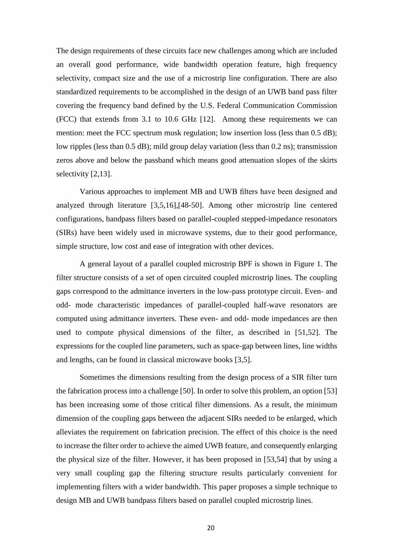
20
The design requirements of these circuits face new challenges among which are included
an overall good performance, wide bandwidth operation feature, high frequency
selectivity, compact size and the use of a microstrip line configuration. There are also
standardized requirements to be accomplished in the design of an UWB band pass filter
covering the frequency band defined by the U.S. Federal Communication Commission
(FCC) that extends from 3.1 to 10.6 GHz [12]. Among these requirements we can
mention: meet the FCC spectrum musk regulation; low insertion loss (less than 0.5 dB);
low ripples (less than 0.5 dB); mild group delay variation (less than 0.2 ns); transmission
zeros above and below the passband which means good attenuation slopes of the skirts
selectivity [2,13].
Various approaches to implement MB and UWB filters have been designed and
analyzed through literature [3,5,16],[48-50]. Among other microstrip line centered
configurations, bandpass filters based on parallel-coupled stepped-impedance resonators
(SIRs) have been widely used in microwave systems, due to their good performance,
simple structure, low cost and ease of integration with other devices.
A general layout of a parallel coupled microstrip BPF is shown in Figure 1. The
filter structure consists of a set of open circuited coupled microstrip lines. The coupling
gaps correspond to the admittance inverters in the low-pass prototype circuit. Even- and
odd- mode characteristic impedances of parallel-coupled half-wave resonators are
computed using admittance inverters. These even- and odd- mode impedances are then
used to compute physical dimensions of the filter, as described in [51,52]. The
expressions for the coupled line parameters, such as space-gap between lines, line widths
and lengths, can be found in classical microwave books [3,5].
Sometimes the dimensions resulting from the design process of a SIR filter turn
the fabrication process into a challenge [50]. In order to solve this problem, an option [53]
has been increasing some of those critical filter dimensions. As a result, the minimum
dimension of the coupling gaps between the adjacent SIRs needed to be enlarged, which
alleviates the requirement on fabrication precision. The effect of this choice is the need
to increase the filter order to achieve the aimed UWB feature, and consequently enlarging
the physical size of the filter. However, it has been proposed in [53,54] that by using a
very small coupling gap the filtering structure results particularly convenient for
implementing filters with a wider bandwidth. This paper proposes a simple technique to
design MB and UWB bandpass filters based on parallel coupled microstrip lines.
21
Figure 1: General layout of a parallel coupled microstrip line BPF; (a) Microstrip transmission line, (b)
General structure of parallel coupled band pass filter
The proposed methodology consists of the following steps: (i) a classical
Chebyshev filter is synthesized on the desired passband; (ii) the initial filter design is
optimized by means of an ad-hoc tool in order to improve loss and rejection values; (iii)
by properly setting a very small or null spacing between adjacent coupled lines of the
optimized filter design, a MB or UWB filter response is obtained.
As an illustration, the described technique has been applied to a two order and a
three order parallel coupled microstrip bandpass filter. By properly setting the resonators
coupling gaps, it was obtained dual- and tri-band filters for the desired frequency bands.
With a suitable configuration, UWB filters resulted covering 40% and 100% of the FCC
band for the two- and three-order filters, respectively. For the MB design, the band
rejection performance is controllable via the coupling gap value.
This work is organized as follows. In Section 2.1.2.2, we detail the basic design
of a two-pole parallel coupled band pass filter centered at 5.78 GHz. In Section 2.1.2.3,
we optimize the previous design with an optimization tool [51,52]. In Section 2.1.2.4, we
show the dual-band and UWB responses obtained by applying small or null coupling gap.
In Section 2.1.2.5, we introduce the theoretical analysis to explain the variable effect of
22
the spacing between coupled lines on the fractional bandwidth of the filter response. In
Section 2.1.2.6 we describe the effect of the coupling gap reduction on the group velocity.
In Section 2.1.3, the same technique is applied to approach the tri-band and UWB versions
of a three-pole band pass filter in order to discuss the advantage of increasing the filter
order.
An ample comparison is offered in Section 2.1.4 regarding the performance results
of this work. Conclusions are elaborated in Section 2.1.5.
2.1.2. Two-pole Chebyshev bandpass filter design
In this section we describe and validate our synthesis theory. The design goal is fabricate
and measure one two-pole MB filter with two bands corresponding to WLAN/WiMAX
frequency bands, and one UWB filter that achieves the greatest possible fractional
bandwidth to cover the FCC specifications.
2.1.2.1. Filter specifications
The design requirements for the initial two order Chebyshev filter are a center frequency
of 5.78 GHz, bandwidth of 125 MHz and passband insertion loss ripple of 0.1 dB,
corresponding to WiMAX systems. The substrate ARLON AD1000x having a
permittivity of 10.2, a substrate thickness of 1.27 mm, and a metallic strip thickness of 35
µm. The implementation requires two microstrip layer.
2.1.2.2. Initial step: two-pole Chebyshev BPF design
The first step of the proposed methodology consists of the classical design of a Chebyshev
parallel coupled band pass filter centered at 5.78 GHz with a bandwidth of 12.5%, order
of N=2 and pass band ripple of 0.1 dB, using dielectric substrate of Arlon AD1000x. This
design required three sections with even- and odd mode characteristic impedances of
eΩ, Ω (section 1,3), and eΩ, Ω (section 2).
The initial physical dimension values – space gap (S), width (W) and length (L) of
each stage – were obtained using the transmission line theory approach developed in [53].
These values will become the input for the optimization design tool used subsequently in
Section 2.2.3.3.
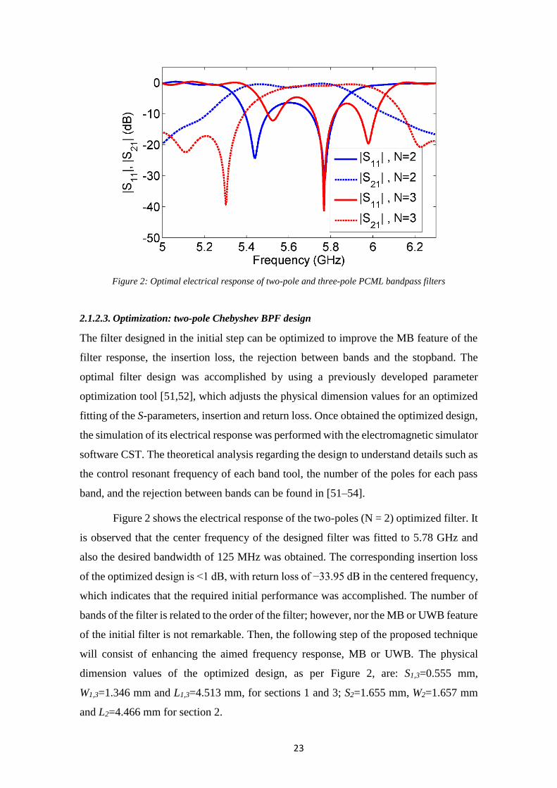
23
Figure 2: Optimal electrical response of two-pole and three-pole PCML bandpass filters
2.1.2.3. Optimization: two-pole Chebyshev BPF design
The filter designed in the initial step can be optimized to improve the MB feature of the
filter response, the insertion loss, the rejection between bands and the stopband. The
optimal filter design was accomplished by using a previously developed parameter
optimization tool [51,52], which adjusts the physical dimension values for an optimized
fitting of the S-parameters, insertion and return loss. Once obtained the optimized design,
the simulation of its electrical response was performed with the electromagnetic simulator
software CST. The theoretical analysis regarding the design to understand details such as
the control resonant frequency of each band tool, the number of the poles for each pass
band, and the rejection between bands can be found in [51–54].
Figure 2 shows the electrical response of the two-poles (N = 2) optimized filter. It
is observed that the center frequency of the designed filter was fitted to 5.78 GHz and
also the desired bandwidth of 125 MHz was obtained. The corresponding insertion loss
of the optimized design is <1 dB, with return loss of −33.95 dB in the centered frequency,
which indicates that the required initial performance was accomplished. The number of
bands of the filter is related to the order of the filter; however, nor the MB or UWB feature
of the initial filter is not remarkable. Then, the following step of the proposed technique
will consist of enhancing the aimed frequency response, MB or UWB. The physical
dimension values of the optimized design, as per Figure 2, are: S1,3=0.555 mm,
W1,3=1.346 mm and L1,3=4.513 mm, for sections 1 and 3; S2=1.655 mm, W2=1.657 mm
and L2=4.466 mm for section 2.
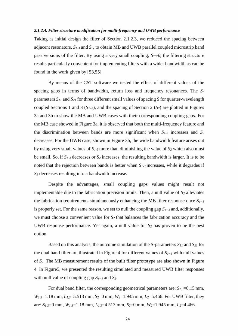
24
2.1.2.4. Filter structure modification for multi-frequency and UWB performance
Taking as initial design the filter of Section 2.1.2.3, we reduced the spacing between
adjacent resonators, S1-3 and S2, to obtain MB and UWB parallel coupled microstrip band
pass versions of the filter. By using a very small coupling, S→0, the filtering structure
results particularly convenient for implementing filters with a wider bandwidth as can be
found in the work given by [53,55].
By means of the CST software we tested the effect of different values of the
spacing gaps in terms of bandwidth, return loss and frequency resonances. The S-
parameters S11 and S21 for three different small values of spacing S for quarter-wavelength
coupled Sections 1 and 3 (S1–3), and the spacing of Section 2 (S2) are plotted in Figures
3a and 3b to show the MB and UWB cases with their corresponding coupling gaps. For
the MB case showed in Figure 3a, it is observed that both the multi-frequency feature and
the discrimination between bands are more significant when S1-3 increases and S2
decreases. For the UWB case, shown in Figure 3b, the wide bandwidth feature arises out
by using very small values of S1-3 more than diminishing the value of S2 which also must
be small. So, if S1-3 decreases or S2 increases, the resulting bandwidth is larger. It is to be
noted that the rejection between bands is better when S1-3 increases, while it degrades if
S2 decreases resulting into a bandwidth increase.
Despite the advantages, small coupling gaps values might result not
implementable due to the fabrication precision limits. Then, a null value of S2 alleviates
the fabrication requirements simultaneously enhancing the MB filter response once S1−3
is properly set. For the same reason, we set to null the coupling gap S1−3 and, additionally,
we must choose a convenient value for S2 that balances the fabrication accuracy and the
UWB response performance. Yet again, a null value for S2 has proven to be the best
option.
Based on this analysis, the outcome simulation of the S-parameters S11 and S21 for
the dual band filter are illustrated in Figure 4 for different values of S1−3 with null values
of S2. The MB measurement results of the built filter prototype are also shown in Figure
4. In Figure5, we presented the resulting simulated and measured UWB filter responses
with null value of coupling gap S1−3 and S2.
For dual band filter, the corresponding geometrical parameters are: S1,3=0.15 mm,
W1,3=1.18 mm, L1,3=5.513 mm, S2=0 mm, W2=1.945 mm, L2=5.466. For UWB filter, they
are: S1,3=0 mm, W1,3=1.18 mm, L1,3=4.513 mm, S2=0 mm, W2=1.945 mm, L2=4.466.

25
(a)
(b)
Figure 3: S-parameters of band pass filter for several space gap values S1,3. (a) Multiband filter (b) UWB
filter
Figure 4: Electrical response of dual-band bandpass filter

26
Figure 5: Electrical response of the implemented UWB bandpass filter
Figure 6a and Figure 6b illustrates the photograph of the fabricated 2-pole filter
prototypes. For the MB case seen in Figure 4, it can be observed that the measured results
show good agreement with the simulation outcomes, with the center frequencies for the
dual band filters at 3.4 GHz and 5.5 GHz covering WLAN and WiMAX bands, according
to the design requirement. From Figure 4, it is noticed that the rejection performance is
controllable via the coupling gap value: the passband bandwidth decreases with
enhancement of rejection between bands, when S1-3 increases. The insertion loss of the
first and second resonance frequency are -0.49 dB and -0.34 dB, respectively. The return
loss is better than -25 dB at both center frequencies. The MB filter has a compact size of
24 mm as total length.
The UWB filter, plotted in Figure 5 demonstrates an operation bandwidth
extended from 3.18 GHz to 6.62 GHz. This response represents a 40% of the amount of
bandwidth defined by the FCC requirements. Within the passband, the measured insertion
loss of the filter is less than 0.35dB ‒ in which 0.16 dB is contributed by the loss due to
the material simulated at 5.00 GHz [50] ‒ whereas the return loss is larger than 10 dB.
2.1.2.5. Influence of coupling gap on the filter FBW
Closed form expressions for modelling the frequency-dependency of even- and odd-
mode characteristics of parallel coupled microstrip line were developed by Hammerstad,
Kirschning and Jansen [53,54], to explain the variation of the calculated fractional
bandwidth (FBW) for several values of coupling gap. For the filter designed in Section

27
2.1.2.3, Table 1 shows the variation of the FBW for different values of the coupling gaps
S1-3 and S2. The fractional bandwidth was achieved by calculating ABCD and S matrixes
indicated in [52]. It can be observed that by decreasing the values of both coupling gaps,
S1-3 and S2, the even impedance characteristic Z0e increases and its related value for odd-
mode Z0o decreases, so leading to a larger value of FBW. Therefore, by properly
decreasing the coupling gap values we can achieve a UWB response. Furthermore, the
combination of parallel coupled resonators and small coupling gap becomes a technique
that offers a great control to select a preferred working bandwidth: the length of each
resonator section allows the shifting of the center frequency and thus the bandwidth can
be re-allocated.
With the aim of achieving a MB response, we observed the effect of modifying
the coupling gap values S1–3 and S2 on the frequency response. For the case with FBW of
41.52 % (S1–3 = 0.088 mm and S2 = 0.163 mm), the analysis is done by increasing the
value of the coupling gap S1–3 or decreasing S2, while the other gap value remains
constant, a dual band response shows up and the bandwidth increases. Figure 7 shows the
theoretically calculated frequency responses of the filter for different values of S2, while
the other gap value remains constant. This figure demonstrates the analysis previously
presented regarding the coupling gap effect on the filter response to yield the MB and
UWB features (the same behavior is observed for calculated S1–3).
Frequency dispersion effect can be studied from [56,57] that mostly affects to the
even-modes. Closed-form expressions for modelling the frequency-dependency of the
even- and odd-mode characteristics of parallel coupled microstrip line were developed by
Hammerstad, Kirschning and Jansen [53,54]. Thus, by considering a small coupling gap,
we increase the gap capacitance Cgd, subsequently decreasing the odd mode phase
velocity Vp,o. A lower phase velocity implies a larger attenuative medium that is translated
into a larger attenuation that will be greater the higher the frequency is.
2.1.2.6. Group delay
In Figure 8 we plotted the simulated group delay for the two-pole filter designed in
Section 2.1.2.3, before the space gap modification. We used the same values of S1–3 used
in Figure 3, with S2 constant and equal to 1.655 mm, to plot the effect of the space gap
variation. The group delay of this filter significantly improves as S1–3 decreases achieving
the better performance for the case of S1–3 = 0.1 mm for which the group delay varies

28
between 0.3 and 0.6 ns. Even when group delay flatness is not required for MB filter, it
is undoubtedly an additional advantage of the proposed approach. One of the requisites
established by the FCC regulations for the UWB devices is a mild group delay variation,
<0.2 ns, through the whole passband. The measured group delay of the UWB filter is also
plotted in Figure 8. Within the passband of the UWB filter, the measured group delay is
flat with the value of 0.24 + 0.01 ns. From the comparison between the frequency
response of the UWB filter and the FCC’s specifications for indoor/outdoor applications,
as aforementioned in Section 2.1.1, we can make some conclusions: (i) the filter presents
a low insertion loss under 0.35 dB; (ii) the group delay of this filter is flat with the value
of 0.24 + 0.01 ns within the passband; (iii) the filter has a compact size of 27 mm as total
length.
We conclude that the technique based on small coupling gap values herein
described allows obtaining both UWB and N-order MB parallel coupled BPFs for any
frequency band and filter order. In the following Section 2.1.3, we applied this technique
based on the small gapping effect to a 3-order parallel coupled band pass filter to obtain
one tri-band bandpass filter and one UWB band pass filters covering the FCC band
extending from 3.1 to 10.6 GHz.
2.1.3. Three-pole Chebyshev band pass filter design
As a second step to illustrate additional details of the synthesis theory and the advantage
of increasing the filter order, we have implemented as initial design a Δ = 10% bandwidth
Chebyshev BPF with centre frequency of 5.78 GHz, with order N = 3 and ripple of 0.1.
The classical design requires eΩ, Ω for sections 1 and 4, and
eΩ, Ω for sections 2.1.2 and 2.1.3. The resulting S-parameters of
this initial three poles (N = 3) filter are also presented in Figure 2. It is observed that the
simulation performance shows a very good agreement with the design specifications. The
center frequency has been fitted to 5.78 GHz with a bandwidth of about 10%. The
corresponding insertion loss of the optimal results is <1 dB with −41.46 dB of return loss
in the desired frequency of 5.78 GHz.
The geometrical parameters values of this optimized filter design obtained as
indicated in Section 2.1.2.2, are: S1,4 =0.608 mm, W1,4 = 1.375 mm, L1,4 = 4.351 mm for
Sections 1 and 4; S2,3 = 1.911 mm, W2,3 = 1.684 mm, L2,3 = 4.30 mm for Sections 2 and 3.

29
(a) (b)
(c) (d)
Figure 6: Photograph of fabricated filters. (a) Dual band bandpass filter, (b) UWB bandpass filter for
N=2, (c) Tri-band bandpass filter, (d) UWB bandpass filter for N=3
Table 1: Calculated FBW for different values of the coupling gaps S1–3 and S2
Coupling gap
(S1,3; S2)
Z0e
Sections (1-3; 2)
Z0o
Sections (1-3; 2)
FBW
(%)
0.43; 1.47 63.94; 50.07 34.83; 39.48 6.92
0.145; 0.469 80.96; 62.79 30.75; 35.19 17.3
0.106; 0263 88.17; 70.91 29.96; 32.82 31.14
0.088; 0.163 93.9; 78.8 29.77; 31.1 41.52
Figure 7: Calculated filter frequency response for different values of S2, S1-3=0.088 mm

30
Similarly to the technique described in Section 2.1.2.2, we studied the effect of
spacing between each symmetrical section to obtain MB and UWB responses. The
performances of the measured and simulated electrical responses of the resulting tri-band
and UWB filters are shown in Figs. 9 and 10, respectively.
Figure 9 shows the tri-band response for several values of the gap S14, taking S23
spacing as null gaping. A relative good agreement between measurement and simulations
for the fabricated case, even that some deviations are present due to the fabrication
tolerances, unideal experimental conditions (not precise simulation of the connectors,
cables, adapters…), and dispersion of the substrate characteristics with respect to the
manufacturer’s datasheet. Furthermore, the rejection between bands and the impedance
bandwidth of selected frequency pass bands result controllable by the S1–3 value.
According to the measured case outcomes shown in Figure 9, three narrow bands were
formed with resonant frequencies centered at 3.2, 5.78 GHz and 8 GHz covering
WiMAX, WLANs and ITU X frequency band (from 7.0 to 11.2 GHz). The corresponding
insertion loss and return loss for the tri-band band pass filter were respectively (−0.82,
−20 dB) at 3.2 GHz, (−0.17, −49.16 dB) at 5.78 GHz and (−0.17, −42.53 dB) at 8 GHz.
It is observed an enhancement of the rejection band in the tri-band response, when S1–4
increases, similarly to the dual-band analysis presented in Section 2.1.2.3.
From Figure 10, it is apparent that the fabricated filter covers the entire UWB band
defined by FCC (3.1–10.6 GHz) and goes beyond 10.6 GHz, with an insertion loss less
than −1 dB within the passband and an even better return less than −40 dB.
The measured group delay of the UWB filter with order N = 3 is also plotted in
Figure 8. Within the passband of the UWB filter, the measured group delay is flat with
the value of 0.23 + 0.005 ns. The physical dimension values of this three-pole Chebyshev
parallel coupled line bandpass filter are: S1,4=0.15 mm, W1,4=0.98 mm, L1,4=4.151 mm,
S2,3=0 mm, W2,3=1.31 mm, L2,3=4.605 mm for the tri-band filter; and S1,4=0 mm,
W1,4=0.98 mm, L1,4=2.85 mm, S2,3=0 mm, W2,3=1.31 mm, L2,3=3.34 for the UWB case.
Figs. 7c and d illustrates a photograph of fabricated filters. The MB filter has a
compact size of 27 mm as total length, and 24 mm for the UWB case.
We concluded that by setting very small coupling between adjacent resonators in
the geometry of parallel coupled bandpass filter, we can easily approach the desired multi-
frequency and UWB responses.
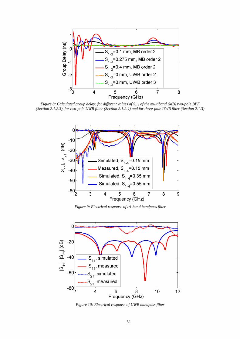
31
Figure 8: Calculated group delay: for different values of S1–3 of the multiband (MB) two-pole BPF
(Section 2.1.2.3), for two-pole UWB filter (Section 2.1.2.4) and for three-pole UWB filter (Section 2.1.3)
Figure 9: Electrical response of tri-band bandpass filter
Figure 10: Electrical response of UWB bandpass filter
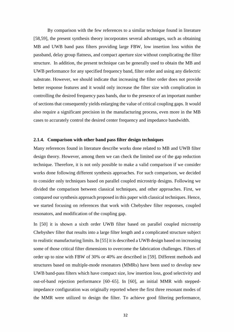
32
By comparison with the few references to a similar technique found in literature
[58,59], the present synthesis theory incorporates several advantages, such as obtaining
MB and UWB band pass filters providing large FBW, low insertion loss within the
passband, delay group flatness, and compact aperture size without complicating the filter
structure. In addition, the present technique can be generally used to obtain the MB and
UWB performance for any specified frequency band, filter order and using any dielectric
substrate. However, we should indicate that increasing the filter order does not provide
better response features and it would only increase the filter size with complication in
controlling the desired frequency pass bands, due to the presence of an important number
of sections that consequently yields enlarging the value of critical coupling gaps. It would
also require a significant precision in the manufacturing process, even more in the MB
cases to accurately control the desired center frequency and impedance bandwidth.
2.1.4. Comparison with other band pass filter design techniques
Many references found in literature describe works done related to MB and UWB filter
design theory. However, among them we can check the limited use of the gap reduction
technique. Therefore, it is not only possible to make a valid comparison if we consider
works done following different synthesis approaches. For such comparison, we decided
to consider only techniques based on parallel coupled microstrip designs. Following we
divided the comparison between classical techniques, and other approaches. First, we
compared our synthesis approach proposed in this paper with classical techniques. Hence,
we started focusing on references that work with Chebyshev filter responses, coupled
resonators, and modification of the coupling gap.
In [50] it is shown a sixth order UWB filter based on parallel coupled microstrip
Chebyshev filter that results into a large filter length and a complicated structure subject
to realistic manufacturing limits. In [55] it is described a UWB design based on increasing
some of those critical filter dimensions to overcome the fabrication challenges. Filters of
order up to nine with FBW of 30% or 40% are described in [59]. Different methods and
structures based on multiple-mode resonators (MMRs) have been used to develop new
UWB band-pass filters which have compact size, low insertion loss, good selectivity and
out-of-band rejection performance [60–65]. In [60], an initial MMR with stepped-
impedance configuration was originally reported where the first three resonant modes of
the MMR were utilized to design the filter. To achieve good filtering performance,
33
stepped-impedance-stub loaded resonator was used, and the designed five-mode UWB
filter had good filtering performance and sharp selectivity, but suffered from narrow
upper stop-band [61]. To improve the upper stop-band performance, an electromagnetic
band gap embedded MMR [62] and harmonic-suppressed MMR, such as stub-loaded
resonators [63] were applied to the design of UWB filters. The size and vertical dimension
of the UWB BPF can be significantly reduced by replacing the modified conventional
one quarter-wavelength parallel coupled lines with cross-shaped coupled lines [64] and
also by the use of radial stub loaded resonator [65], respectively.
Recently, various approaches to implement UWB filters employing distributed
quarter-wave short-circuited stubs have been designed and analyzed [48, 66, 67]. In [48],
compact filters were obtained by folding the connecting lines and using short-circuited
stubs, however the frequency selectivity achieved by these structures was not optimal. In
[66], short-circuited stubs were replaced by open-circuited stubs to accomplish high
selectivity, though the size was increased. In [49, 67], the source-load coupling technique
was used to obtain transmission zeros for a high selectivity and compact size. This
technique has been also applied to other filter types [68, 69].
This set of UWB techniques typically achieves over 100% of FBW with an
excessive complexity of the filter structure and enlarging the filter size. For microwave
wireless communication systems, MB filter design has been an attractive issue, and hence
different dual-band and tri-band filter techniques have been developed. In planar
circuitry, four basic approaches have been considered to add-in multi-frequency feature
in a filter response.
First, by switching between two separate filters at two different frequencies [1];
this approach increases size and cost. Second, by employing stubs to introduce
transmission zeros which separate pass bands [70]; as this is essentially a stop band
approach, far-out-of-band rejection is impossible to attain. Third, by using stepped
impedance resonators, that is [71]; however, it is often difficult to achieve proper coupling
coefficients for a simultaneous, yet independent control of both in-between frequencies
and full bandwidth. The fourth approach consists of coupled resonator pairs [72], however
it lacks an independent option to allocate the transmission zeros. Generally speaking, we
conclude that our approach offers an optimized MB and UWB BPF synthesis design with
good performance in terms of insertion and return losses, gap controllable rejection
performance, short dimensions, low order requirement, and flat group delay response.

34
2.1.5. Conclusions
This contributiion proposes a simple filter synthesis technique valid to design MB and
UWB BPF based on parallel coupled microstrip lines. This technique consists of
modifying the geometry of an initial classical Chebyshev filter by setting a very small or
null coupling gap between adjacent resonators so that a MB or an UWB responses are
obtained. As an example to validate the proposed synthesis approach, this technique has
been applied on two and three order initial Chebyshev filters centered at 5.78 GHz
designed and optimized according to [51,52].
A posteriori, the coupling gap between resonators was varied to reach the final
MB and UWB approaches. We introduced in Section 2.1.2.5 a theoretical analysis based
on the closed forms given in [53,54] to demonstrate and explain the effect of the coupling
gap variation on the multiband and UWB response from the initial design. We also
discussed, for the MB design, how the rejection performance is controllable via the
coupling gap value.
In general, the simulation and measurement results of the filters proposed as
example indicate good agreement in term of S-parameters, insertion and return losses,
and group delay, hence validating the technique developed in Section 2. The synthesis
approach described in this work results in a simple structure very easy to manufacture
with a compact size due to the shorter dimensions and low filter order required, as well
as of low-cost due to the implementation in two-layer PCB technology.
We conclude that the excellent results meet the objective of this part. A good
overall performance is demonstrated for the proposed BPFs in terms of insertion and
return losses within the passbands, as well as FBW and delay group flatness, even
comparing with the requirements established by the FCC regulations. The characteristics
of the resulting filters cannot be extensively compared with those found in literature due
to the limited use of the gap reduction technique. We should note that this technique could
be applied as a complementary step for any design specification, taking as base any
parallel coupled BPF design.
Finally, as main disadvantage we can mention that the UWB filter does not show
good steep skirt selectivity and stopband. The attenuation slopes of the skirts selectivity
are not present in this design. The attenuation slopes of the skirts selectivity could be
improved by insertion of additional poles in the lower and upper stopbands.
35
2.2. Design of Compact Multi-band Bandpass Filter with Suppression of
Second Harmonic Spurious by Coupling Gap Reduction
In this second filter contribution, we describe a method to implement compact multi-band
bandpass filters with suppression of second harmonic frequency. This filter design
approach is based on decreasing the coupling gap between adjacent resonators of a
parallel coupled-line bandpass filter in order to achieve both the desired multi-band
frequency response and the spurious suppression. We present the theoretical analysis of
the proposed structure that consists of modeling the frequency dependence of the even-
and odd-mode characteristic impedances as well as due to the different phase velocities
of the parallel coupled microstrip lines. As an example, a compact tri-band parallel
coupled-line bandpass filter with suppression of second harmonic frequency was
implemented operating at 1.9/3.2/4.6 GHz to cover PCS1900, WiMAX and C-band
applications. A three-pole Chebyshev parallel coupled microstrip bandpass filter was
designed at a center frequency of 3.2 GHz and used as the basis to validate the gapping
effect on the filter response which also achieves a narrower bandwidth for the second
harmonic. Finally, the filter performance with minimized coupling gap is compared to a
filter enhanced by the insertion of apertures in the ground plane. Generally speaking, good
agreement was accomplished between simulated, calculated and measured results.
2.2.1. Introduction
With the progressive development of modern wireless communications, the
radiofrequency spectrum has become increasingly crowded. Wireless transceivers are
required to work in a no single number of bands in order to allow users to adapt a
terminal to achieve different services, and consequently the need for radiofrequency (RF)
multi-band filters has also increased [1,73]. Additionally, features of micro-package,
good performance, low cost and easy to use have been the parallel aim of miniaturization
of bandpass filters [1,2]. In planar circuitry, compact multi-band filters can be
implemented using different basic approaches [73,74]; however, RF filters present a
severe problem of spurious responses mainly due to the presence of the second harmonic
if such conventional designs are used. An undesired response with harmonics gives rise
to asymmetric passband feature that degrades the upper band properties of the filter [17].
The phenomenon of second harmonic spurious response is due to the unequal phase
velocities of the even and odd modes, creating different multiples of the half wavelength
λ0/2 corresponding to the fundamental frequency, for both modes. In a homogeneous

36
transmission line such as a strip line, these half wavelength frequencies are coincident
therefore creating a zero in the filter response at these harmonic frequencies values.
However, the inhomogeneous nature of microstrip does not allow the half wavelength
frequencies to coincide consequently leading to a nonzero response at multiple or
harmonics of the fundamental frequency considered for the filter design (2∙f0, 4∙f0 and so
on). Recently, diverse techniques have been reported and the set of approaches share the
idea of modifying the structure of the microstrip filter by some means, among which we
can mention the use of dielectric overlay, ground apertures insertion, by considering
PBG structures, substrate suppression, periodic grooves design, or use of wiggly line
techniques and filters using fractal shapes [18-20]. In this work, it is proposed an
approach valid to design multi-band parallel coupled bandpass filter with spurious
response suppression at 2∙f0, without changing the basic geometry of the filter structure.
The approach consists of creating small coupling gap between the coupled parallel
sections as a method to accomplish both a multi-band response as well as the second
harmonic reduction. Jointly to this solution, we introduced apertures in the ground plane
[18] and grooves in the substrate [20] in order to compare both techniques – coupling gap
reduction and ground apertures – in terms of suppression of the second harmonic present
in the bandpass filter response.
The theoretical analysis of the solution based on small coupling gap and its effect
on the filter response was detailed in Section 2.2.2. In Section 2.2.3, as an application
example of the proposed filter design technique, we implemented a multi-band filter
operating at the center frequencies of 1.9 GHz, 3.2 GHz and 4.6 GHz used for PCS1900
(Personal communications service), WiMAX (Worldwide interoperability Microwave
Access) and super-Extended C-band systems, respectively. The design procedure
consisted of three steps: from a basic bandpass filter structure to an optimal multi-band
response design with suppression of second harmonic spurious by sequentially integrating
the above indicated two techniques. To this aim, initially a conventional parallel coupled
bandpass filter at 3.2 GHz was designed, as described in Section 2.2.3.1; then, by
implementing a small and null spacing between resonators – coupling gap –, we obtained
a tri-band filter response with spurious minimization, as indicated in Section 2.2.3.2.
Finally, the achieved second harmonic suppression was compared to the enhancement
due to the addition of ground plane apertures and substrate grooves, as shown in Section
2.2.3.3. In Section 2.2.3.4, we discuss the effect of the resonator length on the center
37
resonant frequencies and then on the filter response. The proposed filter was simulated
and optimized using the commercial electromagnetic simulator CST MW. To validate
the performance of the design procedure, a comparison between theoretical and
measurement results is presented showing good agreement and proving that the size,
performance and characteristics of the accomplished multi-band filter have been
optimized.
2.2.2. Theoretical analysis of multi-band filter design
As aforementioned, the approach valid to design parallel coupled bandpass filter with
multi-band response and spurious response suppression at 2∙f0, consists of two combined
techniques: (i) making small coupling gap between the coupled parallel sections to
accomplish the aimed multi-band response and minimize the spurious due to the second
harmonic; and (ii) introducing ground plane apertures and substrate grooves to enhance
the second harmonic suppression. Whilst the second solution has been widely analyzed
in literature, the effect of the first technique is following analyzed to explain its influence
on the filter response.
2.2.2.1. Influence of the small coupling gap on the multiband feature of the filter response
A general layout of a parallel coupled microstrip band pass filter (BPF) is shown in Figure
11. The filter structure consists of open circuited coupled microstrip lines. These coupled
lines are quarter wavelength, (λ/4) long and are equivalent to shunt resonant circuits. The
coupling gaps correspond to the admittance inverters in the low-pass prototype circuit.
Even- and odd- mode characteristic impedances of parallel-coupled half-wave resonators
are computed using admittance inverters. These even- and odd- mode impedances are
then used to compute physical dimensions of the filter [75,51,52]. Designing equations
for the coupled line parameters such as space-gap between lines and line widths and
lengths, can be found in classical microwave books [5,56].
Closed-form expressions for modelling the frequency-dependency of the even-
and odd-mode characteristics of parallel coupled microstrip line were developed by
Hammerstad, Kirschning and Jansen [53,54,76]. Following this formulation, and
considering L the resonator length, W the width and S the coupling gap, the quasi static
even- and odd-mode characteristic impedance of a coupled line, Z0e and Z0o, are
respectively estimated as per (1) and (2):
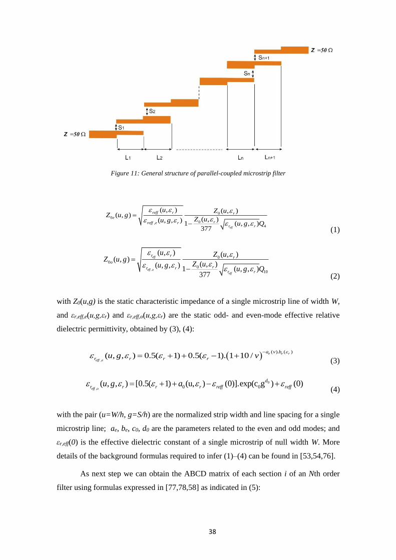
38
Figure 11: General structure of parallel-coupled microstrip filter
00
0,4
( , ) ( , )( , )
( , )( , , )1 ( , , )
377 eff
reff r re
rreff e rr r
u Z uZ u g
Z uu gu g Q
(1)
,
00
010
( , ) ( , )( , )
( , )( , , )1 ( , , )
377
eff
eff o
eff
r r ro
rr rr r
u Z uZ u g
Z uu gu g Q
(2)
with Z0(u,g) is the static characteristic impedance of a single microstrip line of width W,
and εr,eff,e(u,g,εr) and εr,eff,o(u,g,εr) are the static odd- and even-mode effective relative
dielectric permittivity, obtained by (3), (4):
,
( ). ( )( , , ) 0.5( 1) 0.5( 1). 1 10 / e e r
eff e
a v b
r r r ru g v
(3)
,
0
0 0( , , ) [0.5( ) (u1 (0)].exp(c g ) (0, ) )eff or r r r ref
d
ref ffu g a (4)
with the pair (u=W/h, g=S/h) are the normalized strip width and line spacing for a single
microstrip line; ae, be, c0, d0 are the parameters related to the even and odd modes; and
εr,eff(0) is the effective dielectric constant of a single microstrip of null width W. More
details of the background formulas required to infer (1)–(4) can be found in [53,54,76].
As next step we can obtain the ABCD matrix of each section i of an Nth order
filter using formulas expressed in [77,78,58] as indicated in (5):

39
2 2 2 2
0
( )2( )
2
i i i i
i i
i i ii
jqS T q T S
A B sin
C D jTqS
Z
(5)
θ is the electrical length, calculated by (6):
2 refffL
c
(6)
That seen, θ depends on the frequency (f) and on the coupled stage length (L). The
modal phase velocities of all coupled-lines are assumed identical. Detail of formulas q, Ti
and Si formulas are the following:
0 0 0 0
0 0
( ), , ei oi ei oieff i i
Z Z Z Zq cot S T
Z Z
(7)
Note that (Z0ei, Z0oi) are the even- and odd-mode characteristic impedances of the
coupled lines previously calculated for each section i of an Nth order filter. The composite
ABCD matrix of an Nth-order filter can be obtained by successively multiplying the N+1
ABCD matrices calculated as per (5), as following:
1 11 1 2 2
1 11 1 2 2
...N N
N NN
A BA B A BA B
C DC D C DC D
(8)
Finally, the scattering parameters S11 and S21 are determined by (9)-(10):
0
011
0
0
BA CZ D
ZS
BA CZ D
Z
(9)
21
0
0
2S
BA CZ D
Z
(10)
40
Then we conclude that the filter response represented by the S-parameters depends
on the coupling gap, and the smaller the coupling gap is higher the bandwidth filter is
achieved, therefore arising out the multi-band feature of the filter response.
2.2.2.2. Influence of the small coupling gap on the second harmonic spurious suppression
As indicated in [79], for a microstrip edge coupled feature, the phase velocity of the either
even or odd mode, Vp,e and Vp,o, can be approximated by (11)-(12):
,
,even
p even
eff
cV
(11)
,odd
,odd
p
eff
cV
(12)
with c the light speed in free space, and εeff the effective dielectric permittivity for even
and odd modes that can be expressed as a function of the various capacitances as in (13)-
(16):
,
,air
eveneff even
even
C
C
(13)
,odd
odd,air
oddeff
C
C
(14)
'even p f fC C C C (15)
odd p f ga gdC C C C C (16)
where Ceven,air is the capacitance of the microstrip structure when air is used as the
substrate for the even mode, and the same nomenclature applies to the odd mode, Codd,air;
Cp is the parallel plate capacitance; Cf is the fringing capacitance; Cf’ is the fringing in the
even mode only at the magnetic wall; Cga is the gap capacitance due to the coupling in
air; and, Cgd is the gap capacitance in the dielectric substrate. When considering the odd
mode operation, it can be observed that the phase velocity will be affected by the coupled
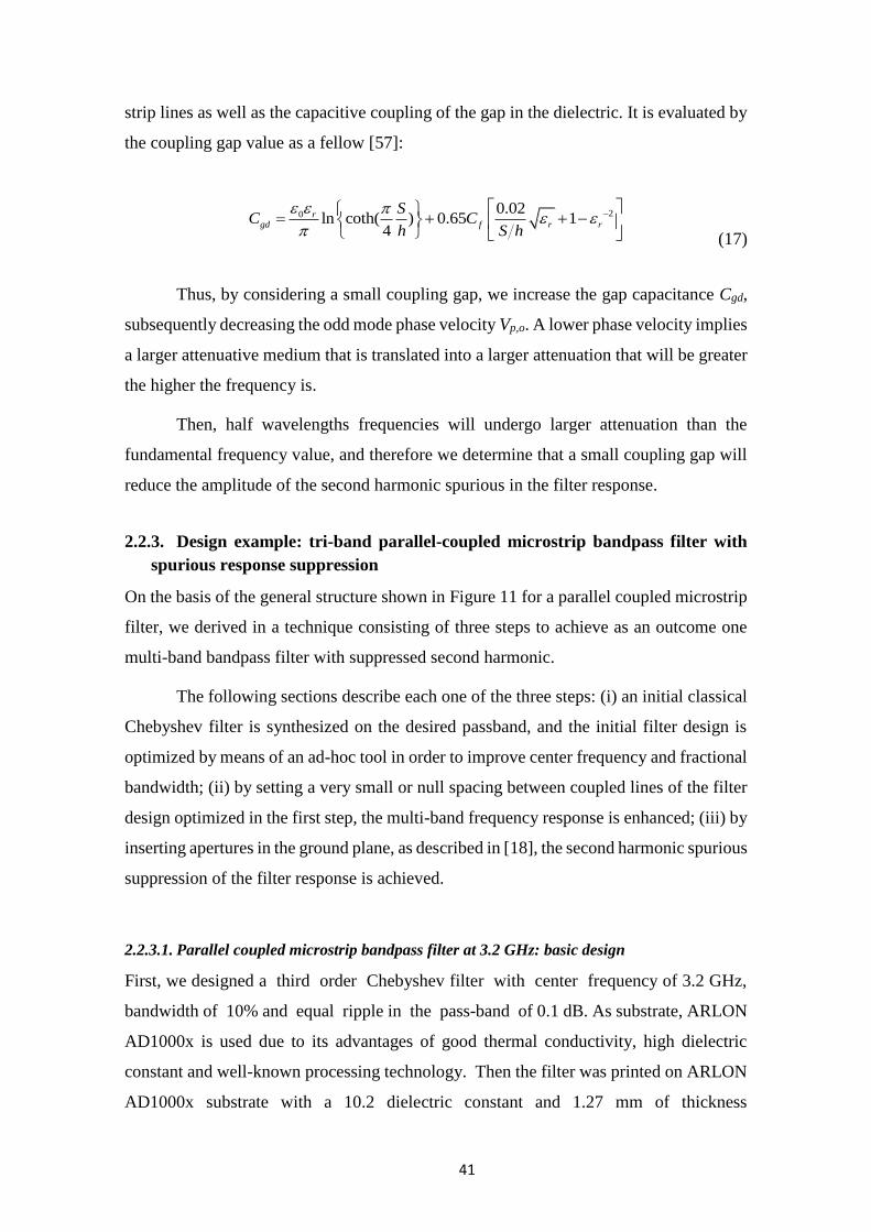
41
strip lines as well as the capacitive coupling of the gap in the dielectric. It is evaluated by
the coupling gap value as a fellow [57]:
20 0.02ln coth( ) 0.65 1
4
rgd f r r
SC C
h S h
(17)
Thus, by considering a small coupling gap, we increase the gap capacitance Cgd,
subsequently decreasing the odd mode phase velocity Vp,o. A lower phase velocity implies
a larger attenuative medium that is translated into a larger attenuation that will be greater
the higher the frequency is.
Then, half wavelengths frequencies will undergo larger attenuation than the
fundamental frequency value, and therefore we determine that a small coupling gap will
reduce the amplitude of the second harmonic spurious in the filter response.
2.2.3. Design example: tri-band parallel-coupled microstrip bandpass filter with
spurious response suppression
On the basis of the general structure shown in Figure 11 for a parallel coupled microstrip
filter, we derived in a technique consisting of three steps to achieve as an outcome one
multi-band bandpass filter with suppressed second harmonic.
The following sections describe each one of the three steps: (i) an initial classical
Chebyshev filter is synthesized on the desired passband, and the initial filter design is
optimized by means of an ad-hoc tool in order to improve center frequency and fractional
bandwidth; (ii) by setting a very small or null spacing between coupled lines of the filter
design optimized in the first step, the multi-band frequency response is enhanced; (iii) by
inserting apertures in the ground plane, as described in [18], the second harmonic spurious
suppression of the filter response is achieved.
2.2.3.1. Parallel coupled microstrip bandpass filter at 3.2 GHz: basic design
First, we designed a third order Chebyshev filter with center frequency of 3.2 GHz,
bandwidth of 10% and equal ripple in the pass-band of 0.1 dB. As substrate, ARLON
AD1000x is used due to its advantages of good thermal conductivity, high dielectric
constant and well-known processing technology. Then the filter was printed on ARLON
AD1000x substrate with a 10.2 dielectric constant and 1.27 mm of thickness

42
corresponding to a middle wafer size. The thickness of the metallic strip was 35 μm. All
the design procedures were with CST MS simulation software. The values of the
characteristic impedances for this initial design were [51,52]: Z0e=63.2863 Ω,
Z0o=41.4723 Ω for sections 1, 4 and Z0e=52.3577 Ω, Z0o=47.4858 Ω for sections 2.2.2,
2.2.3.
Physical dimension values of the initial filter design as gap space (S), width
(W ) and length (L) are: S1−4=0.384 mm, W1−4=1.224 mm, L1−4=8.951 mm, S2−3=1.507
mm, W2−3=1.636 mm and L2−3=8.828 mm [51,52].
Figure 12 illustrates the simulated and measured electrical responses of this filter.
It was observed that the center frequency of the filter was deviated from the specified
frequency value of 3.2 GHz, and then an optimization of the geometrical parameters was
needed. An optimization procedure was applied to the filter design, as described in
[51,52], and the results obtained for the new simulation and measurements outcomes are
shown in Figure 13. It is observed that the center frequency was accurately fit to 3.2 GHz
and the aimed bandwidth of 10% was also attained.
The corresponding insertion loss of the optimized design is less than 1 dB with a
-18 dB of return loss in the desired frequency for simulated results, which indicates that
the design requirements were fully accomplished. Moreover, a good agreement between
simulation and measurement results was achieved.
The geometrical parameter values obtained for the optimized filter design at 3.2
GHz were: S1−4=0.5 mm, W1−4=1.204 mm, L1−4= 8.48 mm, S2−3=1.439 mm, W2−3=1.626
mm and L2−3= 8.361 mm. Photographs of the fabricated filters are shown in Figure 14.
For this first step of the three-steps technique proposed in this work, the physical
dimensions of the filter layout – space gap (S), width (W) and length (L) of each resonator
stage – were obtained using the transmission line theory approach that can be found in
textbooks as in [5]. In [52] a calculator is introduced to automate the calculation of these
design parameters. These values will become the input for the optimization design tool
subsequently used in this first step and indicated in [51,52].
The number of bands of the filter is related to the order of the filter; however, as
shown in Figure 13, the multiband feature of the initial filter is not remarkable. Then, the
following step of the proposed technique will consist of enhancing the multiband
frequency response.

43
Figure 12: S11 and S21 parameters of the initial design of the parallel-coupled microstrip bandpass filter
Figure 13: S11 and S21 parameters of the optimized bandpass filter
(a) (b)
Figure 14: Photographs of the fabricated filters: (a) initial basic design and (b) optimized basic design

44
2.2.3.2. Extension of the filter response to tri-band feature
Once obtained the conventional parallel coupled microstrip bandpass filter designed for
the center frequency of 3.2 GHz, the next step was to analyze the effect on the bandpass
filter response of decreasing the coupling gap between resonators. The main objective of
this step is to enhance the multi-band feature of the filter frequency response.
By means of the CST software we test the effect of different values of the spacing
gaps S1−4 and S2−3, for sections (1-4) and (2-3), in terms of return loss and frequency
resonances. Figure 15 and Figure 16 illustrates the parameters S11 and S21 for different
values of the spacing gaps S1−4 and S2−3, for sections (1-4) and (2-3), respectively. In
Figure 15, the curves corresponding to the return loss – |S11| in dB – demonstrate that the
bandpass filter is sensitive to decreases and increases of the values adopted for S1−4 and
S2−3. We observe that as a result of a coupling gap decrease, the middle band is slightly
affected and then the frequency resonances of other bands are up- or down-shifted.
Additionally, it can be observed that a significant multi-band response shows up and the
difference between the pass bands is more noticeable as the space gap S2−3 value
decreases. For very small values of the space gap S1−4, the impedance bandwidth is
severely affected.
The insertion loss curves – |S21| in dB – demonstrate that the undesired second
harmonic spurious is effectively suppressed due to the small coupling between adjacent
resonators of the filter.
We observed that a very small value of the space gap S2−3 facilitates the trade-off
between the frequency resonance shifting and the multi-band feature appearance.
However, such a value might result not implementable due to the fabrication accuracy
limits. Then, a null value of S2−3 alleviates the fabrication requirements simultaneously
enhancing the multi-band filter response. A resonance frequency shifting occurred due to
the null gap of sections 2.2.2 and 2.2.3, and then the resonator dimensions (length L2,3
and width W2,3) must be redesigned to obtain the aimed center frequency. For this redesign
we used the calculator described in [51,52]. For the coupling gap S1−4 we chose a value
that balances the fabrication accuracy and the impedance bandwidth.
Then we modified the physical dimensions of the optimized basic design given in
Section 2.2.3.1, as following: S1,4=0.15 mm, W1,4=0.604 mm, L1,4=8.38 mm, S2,3=0 mm,
W2,3=1.426 mm, L2,3=7.55 mm.
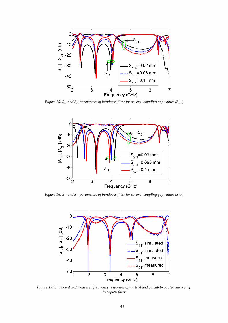
45
Figure 15: S11 and S21 parameters of bandpass filter for several coupling gap values (S1–4)
Figure 16: S11 and S21 parameters of bandpass filter for several coupling gap values (S2–3)
Figure 17: Simulated and measured frequency responses of the tri-band parallel-coupled microstrip
bandpass filter

46
(a) (b)
Figure 18: Photograph of the fabricated tri-band bandpass filter with reduced coupling gap: (a) top layer
and (b) bottom layer
Figure 19: Simulated, measured, and calculated frequency responses of the tri-band BPF with reduced
coupling gap
Figure 17 illustrates the measurement and simulation performance of this
modified tri-band parallel coupled bandpass filter. These plots demonstrate close match
between measured and simulated return loss S11 and the insertion loss S21. As a first result
of the coupling gap decrease, it is observed that the triple-band feature shows up: at 1.9
GHz, 3.2 GHz and 4.6 GHz, i.e. PCS-1900, WiMAX and C-band respectively. The
corresponding insertion loss and return loss for this triple-band bandpass filter were:
-0.05 dB and -32.29 dB at 1.9 GHz, -0.12 dB and - 47.24 dB at 3.2 GHz and -0.12 dB and
-47.11 dB at 4.6 GHz band. Consequently, we conclude that the aim of multi-band
response was accomplished. Photographs of the built filter are shown in Figure 18.
Once determined and tested the physical dimensions of the tri-band bandpass
filter, we calculated the static characteristic impedances for even- and odd mode as given
in (1)-(2): Z0e(u,g)=95.98 Ω, Z0o(u,g)=34.93 Ω for sections (1,4) and Z0e(u,g)=65.08 Ω,

47
Z0o(u,g)=2.7 Ω for sections (2,3). Note that in these calculations of the impedances, we
considered the coupling gap value of section (2, 3) as small as 10-21 instead of zero to
avoid the singularity. Now using these characteristic impedances values along with the
length of each microstrip line of the tri-band band pass filter, we calculated the matrix
ABCD as in (5) and (8). Finally, the S11 and S21 parameters of the tri-band filter were
calculated as in (9)-(10) and represented in Figure 19, showing reasonable agreement
between simulation in CST, measurement and numerical analysis by the formulation
given in Section 2.2.2, that was thus validated.
2.2.3.3. Second harmonic suppression: ground plane apertures insertion
In order to likely enhance the performance of the tri-band bandpass filter obtained in the
previous step, we implemented the classical technique of spurious response suppression
described in [18] that consists of inserting apertures in the ground plane. The filter layout
is shown in Figure 20, and the physical dimensions used for the apertures were: Ws1 =
2∙W1-4 + S1-4 + 0.4 mm, Ws2 = 2∙W2-3 + S2-3 + 0.4 mm, Ls1 = L1-4 - 0.4 mm, Ls2 = L2-3 - 0.1
mm.
The filter performance achieved by adding apertures or slots in the ground plane
was plotted in Figure 21 also showing a comparison with the case without slots achieved
in Section 2.2.3.2 (see Figure 17). It can be checked that the filter response was minimally
affected by comparison to the results presented by the filter without slots. In addition, it
is evident from the same comparison that the second harmonic was not affected by
the insertion of ground apertures. These results demonstrate that the structure introduced
to obtain the tri-band response based on small and null coupling gap was enough to
achieve not only a multi-band response but also a second harmonic suppression not worse
than the given by the classical technique of ground apertures.
As above explained in Section 2.2.2.2, the spurious response was eliminated by
compensating the difference between the phase velocities [79], given that a small
coupling decreases the odd-mode phase velocity. Following (13)-(17), the phase velocity
for the different segment was calculated and the set of single values averaged. The ratio
between odd and even phase velocities Vpo/Vpe was 1.22 for single band filter whilst it
was 0.956 for the triple-band filter so confirming that the decrease of phase velocity is
related to the second harmonic suppression. Photograph of the tri-band bandpass filter
with apertures is shown in Figure 22.
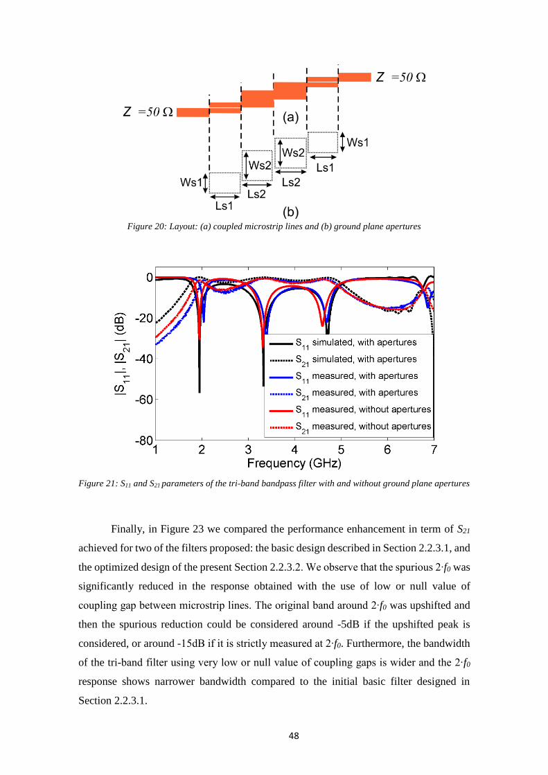
48
Figure 20: Layout: (a) coupled microstrip lines and (b) ground plane apertures
Figure 21: S11 and S21 parameters of the tri-band bandpass filter with and without ground plane apertures
Finally, in Figure 23 we compared the performance enhancement in term of S21
achieved for two of the filters proposed: the basic design described in Section 2.2.3.1, and
the optimized design of the present Section 2.2.3.2. We observe that the spurious 2∙f0 was
significantly reduced in the response obtained with the use of low or null value of
coupling gap between microstrip lines. The original band around 2∙f0 was upshifted and
then the spurious reduction could be considered around -5dB if the upshifted peak is
considered, or around -15dB if it is strictly measured at 2∙f0. Furthermore, the bandwidth
of the tri-band filter using very low or null value of coupling gaps is wider and the 2∙f0
response shows narrower bandwidth compared to the initial basic filter designed in
Section 2.2.3.1.
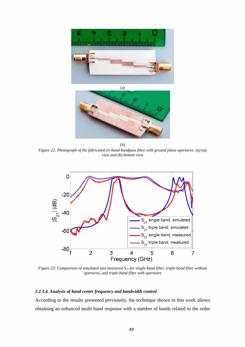
49
(a)
(b)
Figure 22: Photograph of the fabricated tri-band bandpass filter with ground plane apertures: (a) top
view and (b) bottom view
Figure 23: Comparison of simulated and measured S21 for single-band filter, triple-band filter without
apertures, and triple-band filter with apertures
2.2.3.4. Analysis of band center frequency and bandwidth control
According to the results presented previously, the technique shown in this work allows
obtaining an enhanced multi-band response with a number of bands related to the order
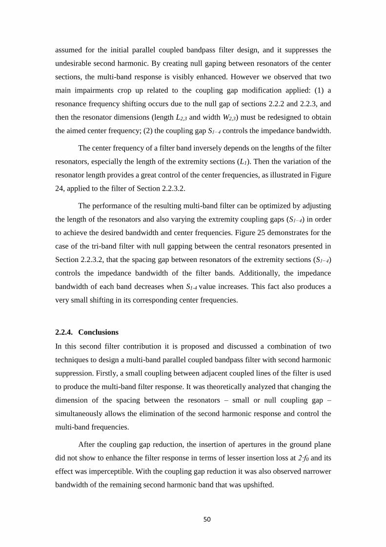
50
assumed for the initial parallel coupled bandpass filter design, and it suppresses the
undesirable second harmonic. By creating null gaping between resonators of the center
sections, the multi-band response is visibly enhanced. However we observed that two
main impairments crop up related to the coupling gap modification applied: (1) a
resonance frequency shifting occurs due to the null gap of sections 2.2.2 and 2.2.3, and
then the resonator dimensions (length L2,3 and width W2,3) must be redesigned to obtain
the aimed center frequency; (2) the coupling gap S1−4 controls the impedance bandwidth.
The center frequency of a filter band inversely depends on the lengths of the filter
resonators, especially the length of the extremity sections (L1). Then the variation of the
resonator length provides a great control of the center frequencies, as illustrated in Figure
24, applied to the filter of Section 2.2.3.2.
The performance of the resulting multi-band filter can be optimized by adjusting
the length of the resonators and also varying the extremity coupling gaps (S1−4) in order
to achieve the desired bandwidth and center frequencies. Figure 25 demonstrates for the
case of the tri-band filter with null gapping between the central resonators presented in
Section 2.2.3.2, that the spacing gap between resonators of the extremity sections (S1−4)
controls the impedance bandwidth of the filter bands. Additionally, the impedance
bandwidth of each band decreases when S1-4 value increases. This fact also produces a
very small shifting in its corresponding center frequencies.
2.2.4. Conclusions
In this second filter contribution it is proposed and discussed a combination of two
techniques to design a multi-band parallel coupled bandpass filter with second harmonic
suppression. Firstly, a small coupling between adjacent coupled lines of the filter is used
to produce the multi-band filter response. It was theoretically analyzed that changing the
dimension of the spacing between the resonators – small or null coupling gap –
simultaneously allows the elimination of the second harmonic response and control the
multi-band frequencies.
After the coupling gap reduction, the insertion of apertures in the ground plane
did not show to enhance the filter response in terms of lesser insertion loss at 2∙f0 and its
effect was imperceptible. With the coupling gap reduction it was also observed narrower
bandwidth of the remaining second harmonic band that was upshifted.
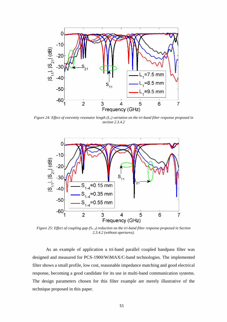
51
Figure 24: Effect of extremity resonator length (L1) variation on the tri-band filter response proposed in
section 2.3.4.2
Figure 25: Effect of coupling gap (S1–4) reduction on the tri-band filter response proposed in Section
2.3.4.2 (without apertures).
As an example of application a tri-band parallel coupled bandpass filter was
designed and measured for PCS-1900/WiMAX/C-band technologies. The implemented
filter shows a small profile, low cost, reasonable impedance matching and good electrical
response, becoming a good candidate for its use in multi-band communication systems.
The design parameters chosen for this filter example are merely illustrative of the
technique proposed in this paper.

52
2.3. Synthesis Design of Bandpass Filter for UWB Applications with
Improved Selectivity
This part presents the design of UWB three-pole modified parallel coupled line bandpass
filter with improved rejection in the out-of-band frequencies. To achieve the desired
UWB requirements using the conventional bandpass filter design, a physical dimension
optimization of space-gap between lines, line widths and lengths was applied. An
equivalent circuit model is also presented and demonstrates reasonable agreement with
simulation results. The optimized filter demonstrates an excellent UWB performance,
covering the Federal Communication Commission spectrum bandwidth with low
insertion loss and acceptable selectivity. However this resulting filter structure presents
very small gapping between adjacent resonators that means the filter is unmanufactured.
Then an example of an alternative filter structure is finally proposed with null gaping and
short-circuited stubs that yields to a fabricated prototype with selectivity improvement.
Generally speaking, reasonable agreement is achieved between measurement and
simulation results.
3.1.1. Introduction
The ultra-wideband (UWB) radio technology has been getting increasingly popular due
to the high-speed high-data wireless connectivity demand. There is a need to design ultra-
wideband bandpass filters covering the whole band permitted by the U.S. Federal
Communication Commission (FCC) that extends from 3.1 to 10.6 GHz [12]. The design
requirements of these circuits face new challenges among which are included an overall
good performance, compact size, wide bandwidth feature and multi-band operation.
Various approaches to implement UWB filters can be found through literature [14,15].
Among other microstrip line centered configurations, bandpass filters based on parallel-
coupled lines have been widely used in microwave systems, due to their good
performance, simple structure, low cost and ease of integration with other devices [50,51].
This work presents the design of a three-pole parallel coupled lines microstrip
bandpass filter (BPF) for UWB applications. The filter design was accomplished in three
steps. First, a filter is designed and optimized to cover the FCC band. The physical
parameter dimensions for this initial design are calculated by an ad-hoc tool [51] and then
optimized in a second design step to achieve a better UWB performance. However this
resulting filter cannot be fabricated due the small spacing between adjacent coupled lines.

53
To solve this limitation, a modified filter structure is proposed in a third design step, by
null gapping the space between all the filter parallel resonators, and incorporating short
circuited stubs.
This final design is manufactured and offers selectivity enhancement, covering
the FCC spectrum with lower insertion loss and group velocity flatness, along with
elimination of the transmission at low frequency. It also presents a size reduction, and it
can be implemented on low cost dielectric substrate of FR4.
3.1.2. UWB bandpass filter: design and results
2.3.2.1. Edge-coupled bandpass filter for UWB applications
According to [52-54], the edge-coupled bandpass three-order filter is designed to cover
the FCC full band, with center frequency of 6.85 GHz, and passband ripple of 0.5. The
filter has been implemented on FR4 substrate with dielectric constant of 4.4 and thickness
of 1.6 mm. As a first step, we define the initial physical dimension values of a bandpass
filter – space gap (S), width (W) and length (L) of each stage –obtained using the
transmission line theory approach as in [51] for a Parallel coupled microstrip line (PCML)
design. These dimensions are, in mm: S1,4=0.1, W1,4=0.54, L1,4=6.34, S2,3=0.14 mm,
W2,3=0.46 and L2,3=6.36 (see Figure 26).
Figure 27a shows the simulated frequency response of the proposed bandpass
filter for both initial and optimized designs, using the CST MWs simulator. It can be
observed that the initial filter design only covers 85% of the FCC band with loss insertion
loss and good rejection; however, the optimized filter case presents a UWB response
working from 3.1 to 10.6 GHz with low insertion loss and relative good rejection. This
improved response is due to the small coupling gap between adjacent filter resonators.
In the next step, we updated the physical dimension values of the optimized filter
design, in mm: S1-4=0.05, W1-4=0.75, L1-4=5.6, S2-3=0.075, W2-3=0.55, L2-3=5.95. The
even- and odd-mode characteristic impedances are: Z0e=1147.33Ω, Z0o=37.41 Ω for
sections (1,4) and Z0e=165.56 Ω, Z0o=43.57 Ω for sections (2, 3).
To determine the equivalent circuit model of this filter type, the L-C components
for the serial and the parallel combination respectively are calculated using the Chebyshev
approximation as per (18)-(19):
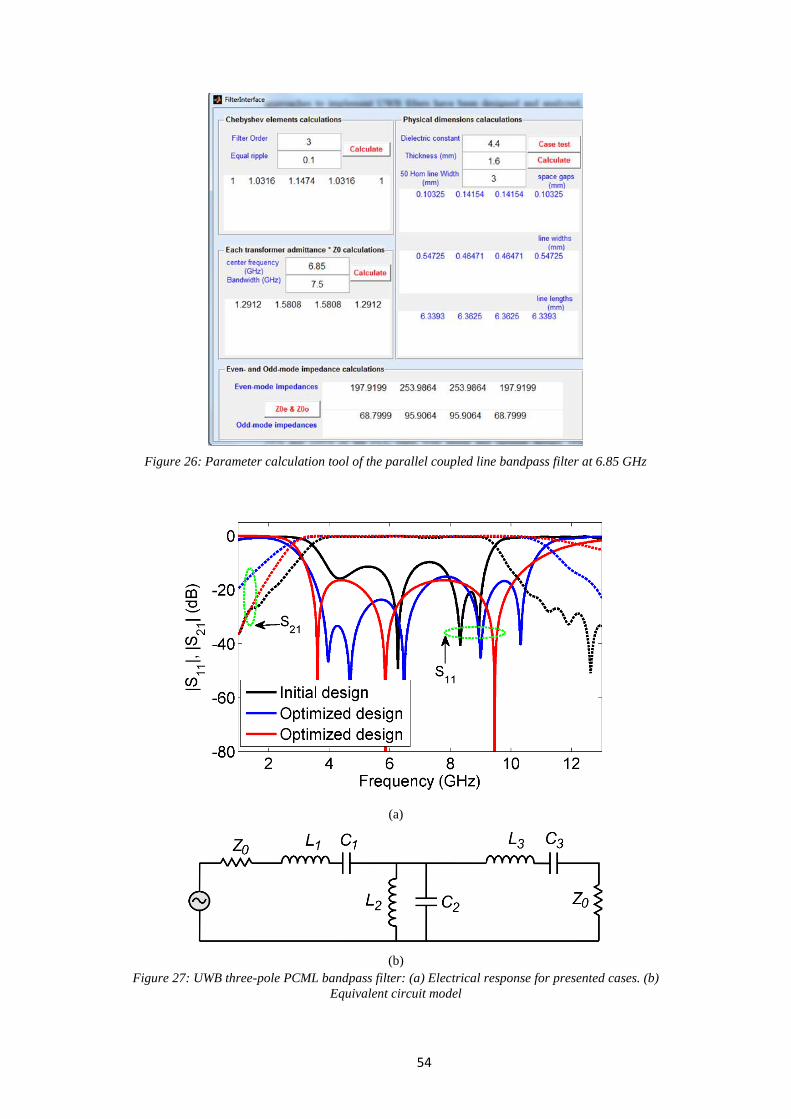
54
Figure 26: Parameter calculation tool of the parallel coupled line bandpass filter at 6.85 GHz
(a)
(b)
Figure 27: UWB three-pole PCML bandpass filter: (a) Electrical response for presented cases. (b)
Equivalent circuit model

55
0
0 0 0
., C
. . .s s
FBW FBWL
Z g Z g
(18)
0
0 0 0
.Z, C
. FBW.Z .p p
FBW gL
g (19)
where g is the Chebyshev element and FBW is the fractional bandwidth, FBW= (ω1∙ω2)/
ω0, with ω0=(ω1∙ ω2)0.5.
Figure 27b shows the equivalent circuit model response for the optimized UWB
PCML bandpass filer. A good agreement between simulation and equivalent circuit
results is clearly observed. The calculated values of the L-C components for the circuit
illustrated in Figure 27b, are: C1=C3= 0.625 pF, C2= 0.545 pF, L1=L3= 1.225 nH, L2= 1.4
nH. The optimized filter was unmanufactured, due to the resulting very small coupling
gap between filter resonators. This geometrical parameter determines the impedance
bandwidth of this filter type [51]. In the following section, a modified PCML bandpass
filter with null gapping and integrated short-circuited stubs is described.
2.3.2.2. Modified UWB bandpass filter with selectivity enhancement
The proposed filter structure consists of setting null gapping between all adjacent PCML
filter resonators and shifting the feed line position to achieve compact filter prototype.
Also two symmetrical short-circuited stubs are incorporated for improvement of rejection
in the out-of-band frequencies and elimination of the transmission at lower frequency
band. In Figure 28, we plotted the geometry of the proposed filter layout without stubs
and photograph of the fabricated prototype. The physical dimension values of this filter
are, in mm: W1=W4= 1.42, L1=L4= 5.8, W2=W3=0.7 and L2=L3= 6.
This prototype was measured using a N5222A Agilent Network Analyzer. The
simulated and measured return loss and insertion of this filter design is plotted in Figure
29. We note that the fabricated UWB bandpass filter demonstrates a low insertion loss
within the FFC band. However, a poor out-of-band rejection performances is seen, due to
the small gaps applied between PCML resonators.
Then an enhancement of filter selectivity is necessary. To solve the limitation of
poor selectivity, we added two symmetrical short-circuited stubs as shown in Figure 30a,
in order to create the desired rejection and eliminate the transmission at low frequency.
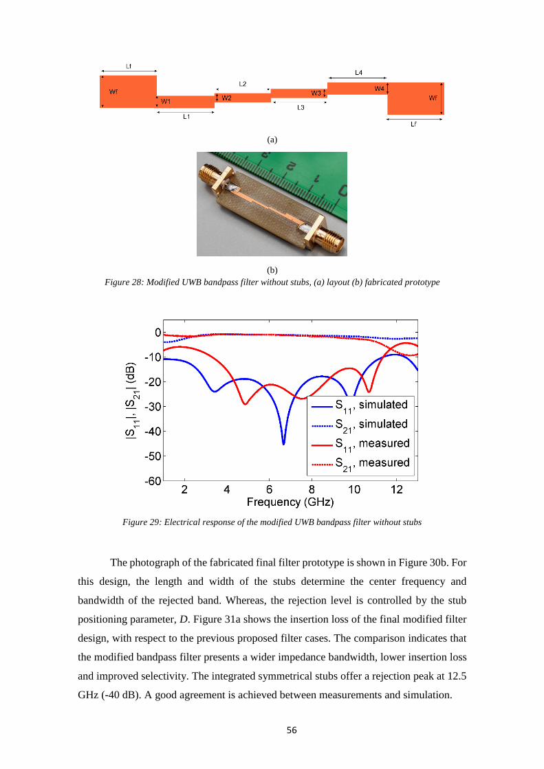
56
(a)
(b)
Figure 28: Modified UWB bandpass filter without stubs, (a) layout (b) fabricated prototype
Figure 29: Electrical response of the modified UWB bandpass filter without stubs
The photograph of the fabricated final filter prototype is shown in Figure 30b. For
this design, the length and width of the stubs determine the center frequency and
bandwidth of the rejected band. Whereas, the rejection level is controlled by the stub
positioning parameter, D. Figure 31a shows the insertion loss of the final modified filter
design, with respect to the previous proposed filter cases. The comparison indicates that
the modified bandpass filter presents a wider impedance bandwidth, lower insertion loss
and improved selectivity. The integrated symmetrical stubs offer a rejection peak at 12.5
GHz (-40 dB). A good agreement is achieved between measurements and simulation.

57
(a)
(b)
Figure 30: Modified UWB bandpass filter with stubs: (a) filter layout, (b) photograph of fabricated
prototype
By comparing to the conventional optimized filter previously presented, the
modified filter offers an enhancement in the UWB impedance bandwidth (5%) with
improved selectivity. However it presents a small increase of the insertion loss (about 1.5
dB), due to the integration of the stubs. Finally, we plotted in Figure 32, the simulated
group delay for the initial, the optimized and the modified filter designs. Within the UWB
passband, both of conventional and modified bandpass filters demonstrate flat values
(<0.2 ns) of group delay, that meet the requirements established by the FCC regulations
for the UWB devices.
2.3.2.3. Results and discussion
Based on the conformal mapping method reported in [53], the even- and odd-mode
characteristic impedances of the coupled line depend on the width W and coupling gap S
of one stage parallel coupled line. When the dielectric constant εr and thickness h of the
substrate are known, the impedances Z0e and Z0o can be calculated as a function of the
strip line width and coupling gap for each stage of parallel coupled lines of the filter.
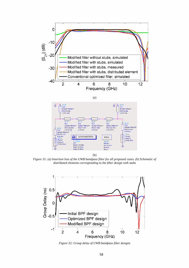
58
(a)
(b)
Figure 31: (a) Insertion loss of the UWB bandpass filter for all proposed cases. (b) Schematic of
distributed elements corresponding to the filter design with stubs
Figure 32: Group delay of UWB bandpass filter designs

59
Table 2: Variation of the calculated FBW in percentage with the small coupling gap values
Coupling gap
(S1,4; S2-3)
Z0e
Sections (1-4; 2-3)
Z0o
Sections (1-4; 2-3)
FBW
(%)
0.048; 0.709 75.45; 58.52 29.96; 37.74 17.52
0.03; 0.292 85.61; 66.86 27.47; 33.44 28.32
0.014; 0.04 100.82; 82.61 26.29; 28.04 43.8
0.0;13 0.015 113.27; 134.1 27.06; 26.29 58.39
Then by decreasing the coupling gap S values, the Z0e values increase, Z0o decrease
and consequently the bandwidth of the parallel coupled line bandpass filter increases.
Detailed analysis and corresponding graphs of the even- and odd-mode impedances are
depicted in [77].
Using the closed formulas developed by Hammerstad, Kirschning and Jansen for
modelling the frequency-dependency of the even- and odd-mode characteristics of a
parallel coupled microstrip line [53,54]. The variation of the static characteristic
impedances for even and odd modes is calculated easily, as well as the fractional
bandwidth (FBW) variation of the PCML filter type. Calculated FBWs in (%), for
different values of the coupling gaps S1-4 and S2-3 are presented in Table 2. This FBW is
obtained by determining the ABCD matrix and S-parameters as indicated in [58], based
on the design specification presented previously. The Three-pole Parallel coupled
microstrip line bandpass filter implements the FR4 substrate with center frequency of
6.85 GHz and passband ripple of 0.5.
However this filter configuration with very small coupling gap kept
unmanufactured. Then we modified our design by setting null spacing between filter
resonators. This resulting structure offers a relative poor selectivity which can be
improved using several techniques, such as the short-circuited stubs here described. This
latter allows eliminating the lower band frequency transmission.
The resonance frequency of the stub is given by (20):
0.52. .( )stub
re
cf
L (20)
60
where L is the total length of the slot, εre is the effective dielectric constant and c is the
speed of light. The dimensions of the short-circuited stubs here used are: Lsl=6.5 mm,
Wsl= 0.4 mm and D=4.6 mm.
3.1.3. Conclusions
In this last chapter part, a modified Parallel coupled microstrip line bandpass filter for
UWB application is presented. Based on a classical design of the Parallel coupled
microstrip line filters, an UWB bandpass filter is first introduced and discussed. Later an
optimized design is obtained demonstrating an improved performance with respect to the
FCC requirements for UWB devices. A low insertion loss with relative good rejection
was obtained within the FCC passband. The equivalent circuit model was also calculated
and good agreement is seen with simulation. However the filter presents very small gap
values so demanding a high accuracy in the manufacturing process not achievable for our
capabilities.
A limit case is proposed with null gapping to yield a fabricated prototype. The
short-circuited stubs are integrated to improve the filter selectivity and eliminate the
transmission at low frequency. Measurements results demonstrate the validity of the
design method proposed in this contribution, achieving an improved performance in terms
of UWB bandwidth, low insertion loss and good rejection band without increasing the
complexity of the filter structure.
The proposed technique is a good candidate for UWB bandpass filter design, and
it can be generally applied to obtain UWB bandpass filters for any specifications. This
work can be extended to achieve a wider rejection in the out-of-band frequencies
regardless the used selectivity enhancement technique. As an example, an array of stubs
with multiple close resonances.
As set-off, the filter width dimension has grown, and as possible solution to this
disadvantage we propose the design of the stub in meander shape. A solution as replacing
stubs by stub-slots in the input feed line would affect the S21 parameter introducing a
larger insertion loss. Despite the disadvantage of the increasing width dimension, the
short-circuited stub is a solution valid to jointly achieve an improved selectivity and the
elimination of the low-frequency transmission.

61
Chapter 3: Band-stop Techniques
for UWB Monopole Antenna design

62
63
3.1. Compact Microstrip Omnidirectional Ultra-wideband Antenna with
Dual Broadband Nested U-shaped Slots and Flat Frequency Response
In this work we present a compact ultra-wideband antenna with dual broadband-notched
characteristics centred at 3.4 and 5.5GHz. The proposed antenna consists of a rectangular
patch with a modified ground plane structure and 50 Ω microstrip-fed line. By etching
two opposite U-shaped slots in the radiating patch, the notched bands of 3.375 – 3.945
GHz for WiMAX and 5.425 – 6.150 GHz for WLAN and HYPERLAN/2 were achieved.
The antenna also offers a flat frequency response so minimising the formation of spurs
and precursors that ensures optimal time domain performance for ultra-wideband radio
applications. The return loss was measured to better than −10 dB over the entire band
from 3.1 to 10.6 GHz. The antenna gain was larger than 2dBi all over the frequencies
with a flatness of 2.5dB and an omnidirectional radiation pattern in the H-plane.
3.1.1. Introduction
The antenna is one of the components which have experienced a significant research
increase in the recent years since that the United State Federal Communications
Commission (FCC) disclosure the ultrawideband (UWB) communication band from 3.1
to 10.6 GHz for commercial use. Besides many challenges related to the UWB antenna
design – from the impedance matching to the compact size and low cost – over the UWB
band there exist some narrowband wireless communication systems which might interfere
to the UWB systems: IEEE 802.16 WiMAX, operating at the 3.3 – 3.7 GHz band, and
IEEE 802.11a WLAN, operating at the 5.15 – 5.85 GHz band, and HYPERLAN/2 at the
5.425 – 6.150 GHz band. Several antenna design methods have been proposed to produce
the band-rejection in the UWB band. Among other approaches, providing UWB antennas
with band-notched characteristic is necessary to solve this emerging problem of
narrowband interference [80-82].
In this contribution, we propose a printed microstrip U-shaped UWB antenna with
dual band-notched configured for the bands of 3.375 – 3.945 GHz (WiMAX) and 5.425
– 6.150 GHz (HYPERLAN/2 and WLAN). The geometry of the achieved UWB antenna
design is simple with compact size and fewer critical parameters. This novel structure
consists of combining a rectangular patch with microstrip line feeding with a modified
ground plane. The dual band-notched operation is achieved by etching two nested U-
shaped slots in the rectangular metal radiating patch. By fine-tuning the width and the

64
total length of each U-shaped slot, the notch center frequency and bandwidth can be
respectively controlled. The dual-band notched design showed an omnidirectional
radiation pattern, and the antenna gain obtained a flatness of 2dB. Finally, the time
domain analysis of the antenna indicated a response which diminishes the formation of
precursor fields [83] superimposed to the transmitted signal.
3.1.2. Antenna design
In Figure 33a, it is shown the geometry and dimensions of the UWB antenna designed
with dual band-notch. In order to obtain a stop-band filtering property, a notch frequency
can be found as per (21):
0.52. .( )notch
re
cf
L (21)
where L is the total length of the slot, εre is the effective dielectric constant and c is the
speed of light. For a dielectric substrate with thickness h, a microstrip line with width w,
and relative permittivity of εre, the effective permittivity can be found by (22):
–0.5
0.5 1 – 1 1 12 /=re r r h w
(22)
Then, by embedding one U-shaped slot in the radiating patch, as shown in Figure
33a, a single stop band of 5.425–6.150 GHz was achieved. This notched band reduces the
interferences from both the IEEE 802.11a and HIPERLAN/2-WLAN systems. The
implemented opposite U-shaped slot, also observed in Figure 33a, produces the second
notched band from 3.375 to 3.945 GHz, for WiMAX systems rejection, without affecting
the first stop band.
Note that the width of the U-shaped slot determines the bandwidth of the rejected
band. The geometry parameters of the dual-band notched UWB antenna design are:
L1=13.5 mm, L2=9.5 mm, L3=3 mm, L4= 26 mm, W1=2.8 mm, W2=14 mm, W3=2.02 mm,
W4=28 mm, n1=0.96 mm, n2=0.74 mm, n3=0.45 mm, m1=3.96 mm, m2=3.19 mm, m3=3.02
mm, Ls1=4.5 mm, Ls2=6 mm, Ws1=7.3 mm, Ws2=13 mm and t=0.2 mm.

65
(a)
(b)
Figure 33: UWB antenna with dual band-notched characteristics: (a) Geometry of the antenna with
detail of ground plane. (b) Photo of the fabricated prototypes.
In Figure 33b, it is shown a photo of three built prototypes: without notched-
bands, single notched band and dual-notched bands, from left to right. The proposed
design approach was printed on low cost FR-4 substrate material with relative dielectric
constant of 4.4, loss tangent of 0.02 and thickness of 1.6 mm. The antenna physical
dimensions correspond to an electrical size of 0.25 λ. For measurements, a 50 Ω SMA
was connected to the feed line.
3.1.3. Measurement results
In Figure 34, we illustrate the measured and simulated values of VSWR for the three
antennas: without notch, single notch and dual notched, respectively. Relative good
agreement between simulation and measurement results can be observed.

66
Figure 34: Comparison of simulated and measured VSWR
(a)
(b)
Figure 35: Radiation pattern for double notched antenna design: (a) E-plane at 3.5 GHz, 6 GHz and 9
GHz. (b) H-plane at 3.5 GHz, 6 GHz and 9 GHz

67
Figure 36: Antenna gain comparison
From Figure 34 it can be seen that the WLAN band at 5.4 GHz is successfully
rejected by introducing the U-shaped slot in the radiating patch antenna. The antenna can
operate through an impedance bandwidth spreading from 3.6 to 11 GHz with a VSWR
less than 2 and with a good rejection at the frequency bands of both WiMAX at 3.4 GHz
and WLAN at 5.5 GHz. Even that not shown, the measured return loss was under −10 dB
over the entire band.
The measured radiation pattern of the antenna with dual band-notched
characteristic is presented in Figure 35. It is observed an omnidirectional performance in
the H-plane, and a like-small dipole in the E-plane.
Finally, in Figure 36 it is shown a comparison of the antenna gain for the three built
prototypes: the gain is over 2 dBi for the entire band with a deviation of 2.5 dB for the
three cases, so resulting in a flat frequency response, considering the ratio of gain flatness
vs bandwidth.
3.1.4. Time domain analysis
As described in [84], the S21(f) parameter of the antenna was estimated and used to
analyze the distortion on a transmitted pulse. The evolution of a signal x(t) transmitted
through the antenna can be evaluated in the frequency domain as in (23):
21 y t IFT S f X f (23)

68
where IFT denotes the Inverse Fourier Transform, and X(f) is the input signal in the
spectrum domain. The input signal consisted of a baseband pulse modulating a sine carrier
with frequency f0 = 7.5GHz. In Table 3 we show the value of the correlation factor in
percentage estimated between the original signals fed into the antenna and the signal
obtained after transmission calculated as in (21). Four different baseband pulses
commonly found in UWB applications have been analyzed for three durations of the pulse
time width Tb – inversely related to the pulse bandwidth -, measured in terms of 1/f0. The
ρ values are given in triplets corresponding to the three antenna cases. The larger input
pulse bandwidth, more critical becomes the effect of the frequency dispersion induced by
the antenna on the input pulse mainly due to the emergence of the precursor field, and
then the correlation factor ρ decreases considerably. The distortion undergone as a result
of the formation of precursor fields derived of the frequency dependence of the antenna
transfer function observed in the response S21(f).
Table 3: Variation of correlation factor in percentage with the transmitted pulse shape and setting
Pulse ρ(%), Tb=10/fc ρ(%), Tb=5/fc ρ(%), Tb=1/fc
Lorentz
0.5/[1+(t/Tb)2]
93, 94, 95 80, 82, 83 22, 27, 32
Impulse
δ(t-0.125 Tb)
<10, <10, <10 <10, <10, <10 <10, <10, <10
Exponential
exp[-2 t/Tb]
74, 80, 85 55, 63, 70 21, 26, 31
Rectangular
Π(t/Tb)
81, 86, 89 66, 74, 80 33, 41, 49
The most favorable case, almost distortion free, is obtained for the Lorentz pulse
given to the lower amplitude level reached by the precursor field formed during the
transmission of this signal that can be explained by the smooth edges of the pulse. The
worst case was achieved for the impulse pulse – configured as a delta function – due to
present a frequency bandwidth as large as the entire band so emphasizing the effects of
the frequency dispersion induced by the antenna response and maximizing the precursor
field formation.
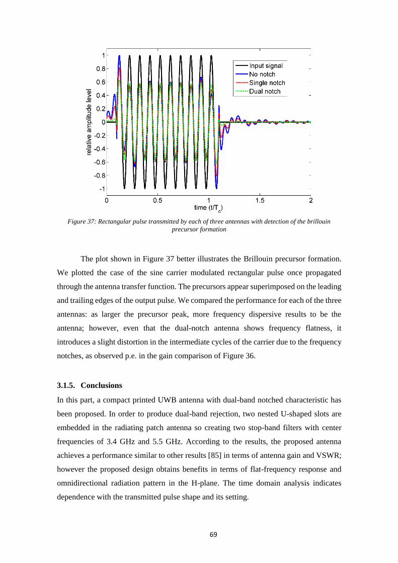
69
Figure 37: Rectangular pulse transmitted by each of three antennas with detection of the brillouin
precursor formation
The plot shown in Figure 37 better illustrates the Brillouin precursor formation.
We plotted the case of the sine carrier modulated rectangular pulse once propagated
through the antenna transfer function. The precursors appear superimposed on the leading
and trailing edges of the output pulse. We compared the performance for each of the three
antennas: as larger the precursor peak, more frequency dispersive results to be the
antenna; however, even that the dual-notch antenna shows frequency flatness, it
introduces a slight distortion in the intermediate cycles of the carrier due to the frequency
notches, as observed p.e. in the gain comparison of Figure 36.
3.1.5. Conclusions
In this part, a compact printed UWB antenna with dual-band notched characteristic has
been proposed. In order to produce dual-band rejection, two nested U-shaped slots are
embedded in the radiating patch antenna so creating two stop-band filters with center
frequencies of 3.4 GHz and 5.5 GHz. According to the results, the proposed antenna
achieves a performance similar to other results [85] in terms of antenna gain and VSWR;
however the proposed design obtains benefits in terms of flat-frequency response and
omnidirectional radiation pattern in the H-plane. The time domain analysis indicates
dependence with the transmitted pulse shape and its setting.

70
3.2. A Simple UWB Tapered Monopole Antenna with Dual Wideband-
Notched Performance by Using Single SRR-Slot and Single SRR-Shaped
Conductor Backed Plane
This paper presents the design of a compact UWB antenna with dual band-notch
characteristics in the 5 GHz band and X-band satellite communications. The proposed
antenna consists of a tapered antenna fed by a microstip feed-line presenting a modified
ground plane to achieve a wide impedance bandwidth, in the interval 2.8-12 GHz, with
VSWR<2. The electromagnetic coupling of the tapered patch with the rectangular split
ring resonator shaped parasitic conductor placed in the ground plane yields the first
frequency notch which ranges from 5.05 to 5.95 GHz, in order to eliminate the dedicated
short-range communications and wireless local area network interferences. The rejection
of the X-band from 7.25 to 8.4 GHz, is achieved by etching a single rectangular split ring
resonator slot in the radiator patch. Prototypes of the proposed antenna design were
measured and compared to simulations, and good agreement was obtained.
3.2.1. Introduction
In the last decades the ultra-wideband (UWB) technology has attracted a great interest
both in the industry and academia research field especially since the Federal
Communication Commission (FCC) allocated the spectrum portion from 3.1 to 10.6 GHz
to be used for commercial purpose of the UWB technology [12]. An enormous attention
has taken place for designing UWB microstrip antenna due to its attractive characteristics
of low profile, miniaturization, capability to be integrated with the design of other
devices, and low cost. Mitigating interference between UWB antennas and co-existing
narrow band systems have prompted the design of UWB antennas doted of frequency
notch filtering characteristics. Different configurations can be found in the scientific
literature proposing the use of planar monopole printed antennas with modified radiator
and/or ground plane in order to achieve a frequency notch characteristic [25-37]. Single,
dual or triple notched frequencies can be obtained by using parasitic elements [25,26],
inserting rod-shaped parasitic structures [27], utilizing a small resonant patch [28],
embedding a slot in the feed line, or cutting different shapes of slots in both the radiation
patch and the ground plane [29-31]. Other designs include split ring resonators (SRR),
and its complementary structure (CSRR), as shaped-slot and/or shaped-conductor, to
produce a desired frequency notch filtering property [32-39].
71
This contribution describes a novel and simple design of a UWB tapered
monopole antenna doted of a dual wideband frequency notch feature. The first notch is
generated at 5.5 GHz by introducing a single SRR-shaped parasitic conductor in the
ground plane to reject the interference due to the dedicated short-range communications
(DSRC) and wireless local area network (WLAN) systems that operate within the range
from 5.15 to 5.925 GHz. A single rectangular SSR-slot is etched in the tapered radiator
to eliminate the wideband interference (7.25-8.4 GHz) corresponding to the uplink and
downlink signals of the X-band satellite communication systems. The modified ground
plane is responsible of achieving the desired wider impedance bandwidth matching over
the entire UWB frequency range. This technique implemented in our design can be
employed on any UWB monopole antenna design doted of a partial ground plane to obtain
any frequency notch requisite with a necessary stopband impedance bandwidth. In the
following subsections we describe the experimental validation with discussion of
measurement results in order to demonstrate the performance of the proposed antenna
design.
3.2.2. Antenna configuration
The geometrical configuration of the proposed UWB tapered monopole antenna is shown
in Figure 38. It consists of a tapered radiation patch with modified ground plane to achieve
the impedance bandwidth matching requisite over the UWB range. The tapered patch was
connected to the microstrip line providing a characteristic impedance of 50 Ω. The
antenna was printed on the Rogers ULTRALAM 2000 high performances substrate with
dielectric permittivity of 2.5, thickness of 0.762 mm and loss tangent of 0.0019. In order
to obtain the frequency notch filtering function and eliminate the undesired frequencies
so avoiding possible interference within the UWB band (3.1 GHz to 10.6 GHz), this
design introduces two additional simple structures in the basic antenna geometry. By
loading the SRR-shaped conductor in the ground plane, we achieve the lower notched-
band at 5-6 GHz. The suppression of the radiation at this notch frequency is due to the
effect of the electromagnetic coupling between the tapered radiator and the single SRR
embedded on the radiator backside. The higher notched-band 7.25-8.4 GHz is obtained
by embedding a single rectangular SRR-slot in the tapered patch. Moreover the stop-band
property can be controlled by adjusting the width and the length of the SRR element for
both cases [86,87].

72
Figure 38: Schematic of the proposed antenna design: (a) radiator tapered element; (b) modified ground
plane; (c) rectangular CSRR-shaped slot; (d) rectangular SRR-shaped parasitic conductor
Figure 39: Configuration of the antennas used for our study: top and bottom layers
Simulation results have been obtained with the CST MW StudioTM. Figure 39
illustrates the three stages of the antenna design. Initially, a reference UWB tapered
monopole antenna is designed without notch band characteristics (antenna#1). Later this

73
configuration is modified to introduce the rejection of a single band by loading a SRR-
shaped parasitic conductor in the ground plane (antenna#2). Finally, the dual-band
notched UWB antenna is achieved loading the SRR-shaped parasitic conductor in the
ground plane and etching the SRR-slot in the tapered patch, and it is presented as
antenna#3. The SRR and CSRR elements embedded within the antenna are designed by
considering the corresponding resonant frequency derived from their respective quasi-
static resonance [43]. The specific geometrical details of each element are provided in the
following section.
3.2.3. Measurement results
Following we compare the performance of the three stages of the antenna design: the
reference design case (antenna#1), single notched band case (antenna#2), and the dual-
band notched case (antenna#3).
3.2.3.1. UWB tapered monopole antenna
Figure 40 shows the VSWR performance of the basic UWB tapered monopole antenna
without any embedded notch filtering element. As can be seen in the plot, the UWB
antenna operates from 2.8 to 12 GHz with a voltage standing wave ratio (VSWR) lower
than 2. Good agreement between the measured and simulated plots is inferred from the
comparison. The parameters of the UWB reference antenna without notch function are,
in mm: L1=20, L2=10.8, L3=13, L4=20, L5=2, W1=30, W2=2.2, W3=8, W4=6, W5=2.5.
3.2.3.2. UWB tapered monopole antenna with single band-notch
In order to reject the WLAN/DSRC frequencies (5.05-5.95 GHz), we loaded a single
SRR-shaped parasitic on the backside of the tapered patch, so obtaining the namely
antenna#2 case. This notch filtering property is due to the electromagnetic coupling
occurring between the radiating patch element and the resonant SRR-shaped parasitic
element. The selection of critical parameters of the SRR structure is related to important
effects arising on the antenna performance.
Figure 41 shows the VSWR of antenna#2 obtained for different values of the total
length of the SRR-shaped parasitic, given by Lt = Ls + Ws. It can be observed that when
the total length of the SRR structure increases, the center of the notch frequency decreases
74
without affecting the stop-band impedance bandwidth. Then, the notch frequency is
controllable by varying the total length Lt of the embedded SRR-shaped parasitic.
Furthermore, the band rejection is influenced by the width of the SRR-shaped parasitic,
Ds. This effect was investigated and shown in Figure 42. We observe that the notched
frequency depends of the SRR-shaped parasitic width Ds, in a similar way to that one due
to the influence of the total length Lt, as previously described.
The capacitive coupling between the introduced SRR-shaped parasitic and the
modified ground plane also affects the stop-band performance, as illustrated in Figure 43.
We can deduce that the impedance bandwidth of the stop-band increases as the distance
d1 between the ground plane and the SRR-shaped parasitic element decreases. Rejection
levels are enhanced when distance d1 decreases, corresponding to an intensification in
the effective capacitive value provided by the gap between the antenna and the SRR
loading element [43]. Thus the variation of the distance d1 introduces an easy way for
controlling both the stop-band impedance bandwidth and the corresponding maximum
value of VSWR. The values of the design parameters selected for the SRR-shaped parasitic
conductor backed-plane are as following, in mm: Ws=15.7, Ls=6.6, Gs=0.8, Ds=0.8 and
d1=0.3.
Figure 44 shows comparison between the simulated and measured VSWR
characteristics of the single- band-notched UWB antenna (antenna#2) and the reference
antenna (antenna#1). This plot clarifies that the achieved notched frequency bandwidth
is achieved from 5.05 to 5.95 GHz with a maximum VSWR higher than 10. Obviously,
the achieved notched bandwidth can suppress the DSRC and WLAN bands for UWB
communications.
3.2.3.3. Dual band-notched UWB tapered monopole antenna
The next step was to achieve a dual band notched feature to reject the uplink and downlink
signals of the X-band satellite communications. Then, a SRR-slot was etched in the
tapered patch, as shown in Figure 39, so obtaining the namely antenna#3 case. The
proposed dual band-notched UWB antenna was fabricated and tested. The measured and
simulated VSWR of the antenna#3 are illustrated in Figure 45. It can be seen that for this
case the impedance bandwidth is 8.2 GHz, covering the band 2.8-11 GHz along to
achieving the required dual band-notched performance.

75
Figure 40: Simulated and measured VSWR for antenna#1
Figure 41: Simulated VSWR for antenna#2 with different values of Lt.
Figure 42: Simulated VSWR of antenna#2 for different values of Ds with Lt = 22.3 mm

76
Figure 43: Simulated VSWR for antenna#2 with different values of d1. Lt=22.3, Ds=0.8 (mm)
Figure 44: Simulated and measured VSWR of the proposed UWB antenna with single frequency notch
Figure 45: Simulated and measured VSWR of the proposed dual bad-notched UWB antenna
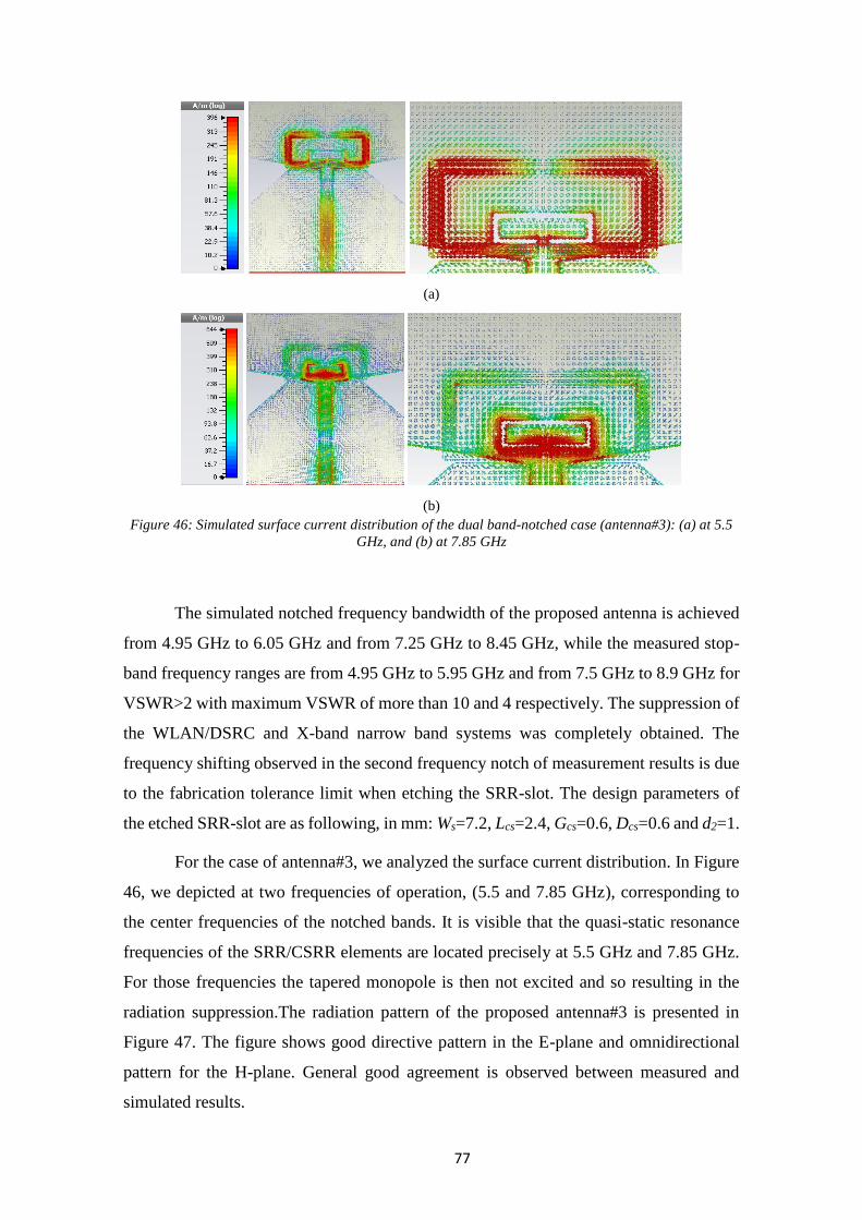
77
(a)
(b) Figure 46: Simulated surface current distribution of the dual band-notched case (antenna#3): (a) at 5.5
GHz, and (b) at 7.85 GHz
The simulated notched frequency bandwidth of the proposed antenna is achieved
from 4.95 GHz to 6.05 GHz and from 7.25 GHz to 8.45 GHz, while the measured stop-
band frequency ranges are from 4.95 GHz to 5.95 GHz and from 7.5 GHz to 8.9 GHz for
VSWR>2 with maximum VSWR of more than 10 and 4 respectively. The suppression of
the WLAN/DSRC and X-band narrow band systems was completely obtained. The
frequency shifting observed in the second frequency notch of measurement results is due
to the fabrication tolerance limit when etching the SRR-slot. The design parameters of
the etched SRR-slot are as following, in mm: Ws=7.2, Lcs=2.4, Gcs=0.6, Dcs=0.6 and d2=1.
For the case of antenna#3, we analyzed the surface current distribution. In Figure
46, we depicted at two frequencies of operation, (5.5 and 7.85 GHz), corresponding to
the center frequencies of the notched bands. It is visible that the quasi-static resonance
frequencies of the SRR/CSRR elements are located precisely at 5.5 GHz and 7.85 GHz.
For those frequencies the tapered monopole is then not excited and so resulting in the
radiation suppression.The radiation pattern of the proposed antenna#3 is presented in
Figure 47. The figure shows good directive pattern in the E-plane and omnidirectional
pattern for the H-plane. General good agreement is observed between measured and
simulated results.
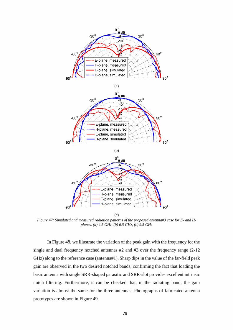
78
(a)
(b)
(c)
Figure 47: Simulated and measured radiation patterns of the proposed antenna#3 case for E- and H-
planes. (a) 4.5 GHz, (b) 6.5 GHz, (c) 9.5 GHz
In Figure 48, we illustrate the variation of the peak gain with the frequency for the
single and dual frequency notched antennas #2 and #3 over the frequency range (2-12
GHz) along to the reference case (antenna#1). Sharp dips in the value of the far-field peak
gain are observed in the two desired notched bands, confirming the fact that loading the
basic antenna with single SRR-shaped parasitic and SRR-slot provides excellent intrinsic
notch filtering. Furthermore, it can be checked that, in the radiating band, the gain
variation is almost the same for the three antennas. Photographs of fabricated antenna
prototypes are shown in Figure 49.

79
Figure 48: Peak gain for the three cases of UWB tapered antennas
(a) (b)
Figure 49: Photograph of prototyped antennas: (a) Top later (b) bottom layer. Left: Antenna1. Center:
Antenna 2. Right: Antenna 3
3.2.4. Conclusions
A simple and symmetric tapered monopole UWB antenna with a single SRR-shaped
parasitic and single SRR-slot etched in the tapered patch, exhibiting dual-frequency notch
performance is presented in this work. The electromagnetic coupling between the tapered
patch and the SRR-shaped parasitic introduced on the back side of the tapered element,
yields the first notch at 5.5 GHz, with a large bandwidth, filtering the interferences due
to the co-existence of DSRC/WLAN systems. Moreover, the uplink and downlink signals
of the X-band satellite communication systems are rejected by embedding a single SRR-
slot on the radiation patch. The notched frequencies can be easy controlled by modifying
the dimensions of the SRR structures. Fabricated antennas demonstrate overall good
match between simulated and measured results. In summary, a simple design procedure,
valid to obtain a good omnidirectional radiation pattern, with relative stable gain and low
profile, as well as manufacturable at low cost make the proposed antenna a suitable
candidate for UWB systems needed of multiple frequencies notches.
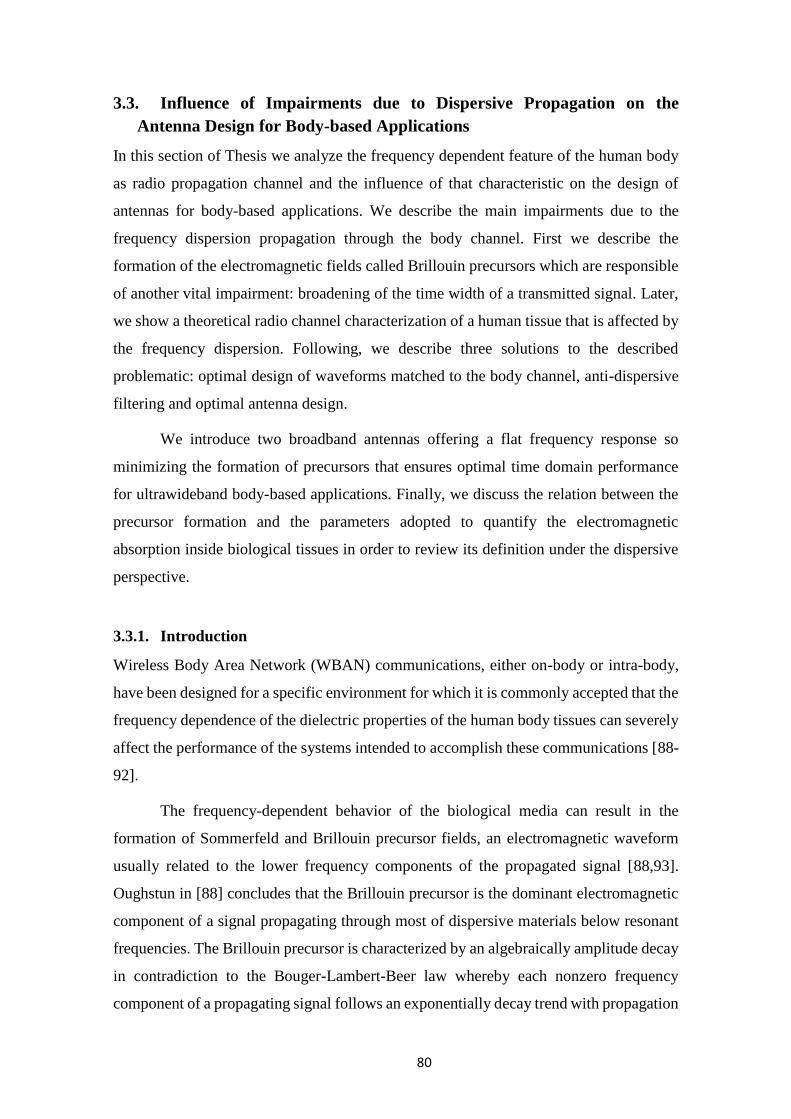
80
3.3. Influence of Impairments due to Dispersive Propagation on the
Antenna Design for Body-based Applications
In this section of Thesis we analyze the frequency dependent feature of the human body
as radio propagation channel and the influence of that characteristic on the design of
antennas for body-based applications. We describe the main impairments due to the
frequency dispersion propagation through the body channel. First we describe the
formation of the electromagnetic fields called Brillouin precursors which are responsible
of another vital impairment: broadening of the time width of a transmitted signal. Later,
we show a theoretical radio channel characterization of a human tissue that is affected by
the frequency dispersion. Following, we describe three solutions to the described
problematic: optimal design of waveforms matched to the body channel, anti-dispersive
filtering and optimal antenna design.
We introduce two broadband antennas offering a flat frequency response so
minimizing the formation of precursors that ensures optimal time domain performance
for ultrawideband body-based applications. Finally, we discuss the relation between the
precursor formation and the parameters adopted to quantify the electromagnetic
absorption inside biological tissues in order to review its definition under the dispersive
perspective.
3.3.1. Introduction
Wireless Body Area Network (WBAN) communications, either on-body or intra-body,
have been designed for a specific environment for which it is commonly accepted that the
frequency dependence of the dielectric properties of the human body tissues can severely
affect the performance of the systems intended to accomplish these communications [88-
92].
The frequency-dependent behavior of the biological media can result in the
formation of Sommerfeld and Brillouin precursor fields, an electromagnetic waveform
usually related to the lower frequency components of the propagated signal [88,93].
Oughstun in [88] concludes that the Brillouin precursor is the dominant electromagnetic
component of a signal propagating through most of dispersive materials below resonant
frequencies. The Brillouin precursor is characterized by an algebraically amplitude decay
in contradiction to the Bouger-Lambert-Beer law whereby each nonzero frequency
component of a propagating signal follows an exponentially decay trend with propagation

81
distance [93]. This feature implies that a travelling signal which can ensure the forerunner
formation could reach a larger propagation distance inside the medium of interest. Despite
becoming a known phenomenon [88,89,91-95], it has not been usual to relate the body-
based technologies and the precursor wave emergence which would be expectable
especially if a large frequency bandwidth or low-frequency EM waves are considered. It
is in the lower region of the spectrum where the precursor formation becomes stronger.
In Figure 50, we illustrate the concept of the precursor formation. We considered
a rectangular input pulse (in blue) modulating a sinusoidal carrier that once travels
through the human body undergoes the dispersive spread so leading to the precursor
formation which is visible as superimposed fields in the leading and trailing edges of the
red waveform.
The dispersive propagation undergone by the signal travelling through a medium
such as the body-channel can strongly condition the received signal due to produce
undesired effects, the main of which is the broadening of the time duration undergone by
the signal propagating through the dispersive media, so turning the frequency dispersion
into an extremely important impairment to be considered in the design of receiver systems
[91, 96], or in order to ensure the reliability of the propagation through this kind of media,
as the case of intra-body communications. e.g., for the case of a sequence of pulses, at a
given propagation distance, the broadening experienced by a travelling pulse in its time
width can lead to a destructive merge of the information which would make impossible
and totally erroneous the information retrieval [96]. This phenomenon depends on the
dielectric properties of the underlying medium as well as on other parameters or settings,
e.g. the input signal type and its configuration, as well as the involved transmitted and/or
received bandwidth [88,96].
In Section 3.4.3, we describe the main impairments due to the precursor formation
and their effects on the body-based applications, mainly from the point of view of intra-
body radio propagation. We also considered solutions to such problematic. In Section
3.4.3.4, we introduce the time domain analysis of two frequency-flat response antennas
designed to diminish the formation of precursor fields as well as to avoid distorting the
transmitted pulses. In Section 3.4.4, we discuss the power extinction decay trend for intra-
body radio channel and its relation to the specific absorption rate (SAR). Finally,
conclusions are offered in Section 3.4.5.
82
Figure 50: Illustration of the Brillouin precursor formation (in red) once a properly configured input
signal (in blue) propagates through the human body
3.3.2. Formulation of dispersive propagation
Here we reflect on the most important aspects and impairments related the frequency
dispersion and the precursor formation, as well as we describe three approaches valid to
solve the created problematic.
3.3.2.1. Radio channel characterization for a dispersive medium
The frequency dispersive nature of the body channel alters the propagation of wideband
or low-frequency signals and therefore can reach distort the radio channel
characterization of intra-body radio propagation: the broadening and amplitude level
distortion undergone by the transmitted pulses will introduce uncertainty or noise, leading
to a larger degradation of the cross-correlation function (CCF), and consequently masking
the return echoes detection [92].
This fact especially affects broadband communications, for which multipath
interference can be difficult to characterize and control. Different solutions are following
described.

83
3.3.2.2. Optimal transmitting waveform design
The evolution of an input signal x(t) was evaluated in the frequency domain in off-line
mode, just considering the frequency response of the dispersive medium H(z,f), and the
propagation distance travelled z inside the medium. Then, it is enough to multiply
Y(f)=X(f)∙H(f), where X(f) is the input signal in the spectrum domain, and then apply an
Inverse Fast Fourier Transform to observe the output signal in the time domain, y(t). The
estimation of the frequency response H(z,f) of the dispersive medium agrees a general
transmission coefficient definition as described in (24) [91,96]:
zfj mefzH)(
),(
(24)
with γm(f) the medium propagation constant derived as in (25):
rmc
j (25)
The outcome H(z,f) contains information about the effects of attenuation and
phase for each frequency component of the signal travelling through the medium under
study. The result is then a frequency filter H(z,f) and is valid for analysis of precursor
evolution for any input signal x(z,t) propagating through the dispersive medium
characterized by H(z,f) for any penetration depth z. The model representing the complex
dielectric properties of the underlying dispersive media is of vital importance since it is
used to estimate the propagation constant γm(f) in (25). The dielectric properties will
fingerprint indeed the resulting Brillouin precursor.
In Figure 51 we show the theoretical evolution of a rectangular pulse provided of
a sine carrier with center frequency f0=6GHz, and time duration Tb=10/f0 through a single
layer of tissue N1 characterized by a Cole-Cole model [97]. We observe the large
waveform shape distortion, as well as the early extinction of the carrier component (cycles
within edges). This result is particularly important for intra-body communications. It
implies that a wideband transmission will be severely affected by the dispersive
propagation and robust input signals and proper spectrum frequency windows must be
chosen [96].

84
Figure 51: Theoretical evolution of a rectangular pulse after propagating through different distances
within a layer of tissue N1: at input (z=0), z=1∙zd, z=5∙zd and z=9∙zd, with zd=e-α, and α the propagation
constant of the tissue in Np
For intra-body communications, the form and shape of the information-bearing
transmitted signal is an important factor to consider [98,99]. Since the transmitted signal
influences the formation and performance of the resulting precursor, we can conclude that
a medium-matched signal can lead to optimal performance by combining the benefits of
the precursor formation (larger amplitude) with minor impairments (lesser time duration
broadening) [99].
3.3.2.3. Anti-dispersive filtering
As in radar technology, an anti-dispersive (AD) filtering can be implemented on the
receiver end to compensate the frequency dispersive effects [98]. However, this solution
requires the a priori knowledge of the propagation scenario, also in terms of multipath
characteristics. On the transmitter end, an AD element [100] could be also considered as
an element prior to the antenna or well embedded on it, in order to match the signal to a
specific medium and propagation scenario, so achieving a signal propagation in frequency
flat mode; however this solution is also a pulse shaping technique that does not prevent
the need to use an AD filtering on the receiver end. However, it should be noted that AD
elements are very sensitive to design errors and variations of the medium dielectric
properties. Solutions presented in [98] also accounts for the variation of the tissues
response with the distance propagated by the signal within them [100].
0 1 2 3 4 5 6 7 8 9 10-1
-0.8
-0.6
-0.4
-0.2
0
0.2
0.4
0.6
0.8
1
time (t/Tb)
rela
tive
am
plit
ud
e(V
)
Input signal
Rect, Tissue N1, Cole-Cole, Tb=10/f
0, z=1z
d
Rect, Tissue N1, Cole-Cole, Tb=10/f
0, z=5z
d
Rect, Tissue N1, Cole-Cole, Tb=10/f
0, z=9z
d

85
3.3.2.4. Antenna design
The antenna can be also used as an AD element, or simply can be designed to show a flat-
frequency response in order to avoid worsening the impairments due to the frequency-
dependent body channel. Following we describe two antennas designed and built with
flat-frequency response and improved time domain performance (Figure 52). The first
antenna model selected to be implemented was a UWB ridged horn. Material selected
was a blend of copper and brass (40%, 60%), and in the waveguide-to-coaxial adaptor it
was used an N male connector. The UWB horn antenna dimensions are (in mm):
Ha=46.67, Wa=66.67, Lf=53.33, Hg=9.467, Wg=14.95, Lg=5.2, Wr=4.88, Sr=666.7,
Lsr=3.333, Hsr=473.3, Wc=0.976, Sf=1.017, θc=45°, Di=0.4167, Do=1.367. The relative
dielectric permittivity of the coaxial feeder was εr=2.05.
The UWB horn can operate in the range 3 to 11GHz, with a VSWR less than 1.5,
and the return loss was under -15dB. The antenna gain was 9.7 dBi (@7GHz) with a
deviation of 2.7 dBi. The antenna beam width was 56.81° (E-plane) and 52.72° (H-plane).
Both parameters were obtained from measurements in an anechoic chamber. For the
printed UWB antenna the geometry parameters were (in mm): L1=13.5, L2=9.5, L3=3, L4=
26, W1=2.8, W2=14, W3=2.02, W4=28, n1=0.96, n2=0.74, n3=0.45, m1=3.96, m2=3.19,
m3=3.02. The antenna was printed on low cost FR-4 substrate material with relative
dielectric constant of 4.4, loss tangent of 0.02 and thickness of 1.6 mm. The antenna
physical dimensions correspond to an electrical size of 0.25λ. The printed UWB antenna
can operate through an impedance bandwidth ranging from 3.6 to 11GHz, with a VSWR
less than 2, and a measured return loss was under −10 dB over the entire band. The
measured radiation pattern was omnidirectional performance in the H-plane, and a like-
small dipole in the E-plane. The antenna gain is over 2dBi for the entire band with a
deviation of 2.5dB, so resulting in a flat frequency response, in terms of gain flatness vs
bandwidth (Figure 53).As described in [101], the S21(f) parameter of the printed UWB
antenna was measured under free-space conditions inside an anechoic chamber, for the
maximum antenna gain direction, and later used to estimate the influence of the radiating
element on the transmitted pulse. The evolution of a signal x(t) transmitted through the
antenna can be evaluated in the frequency domain in off-line mode. It is enough to
multiply Y(f)=X(f)∙s21(f), where X(f) is the input signal in the spectrum domain, and then
apply an Inverse Fast Fourier Transform to observe the output signal in the time domain,
y(t).
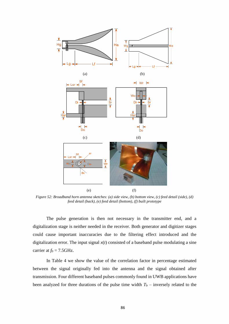
86
(a) (b)
(c) (d)
(e) (f)
Figure 52: Broadband horn antenna sketches: (a) side view, (b) bottom view, (c) feed detail (side), (d)
feed detail (back), (e) feed detail (bottom), (f) built prototype
The pulse generation is then not necessary in the transmitter end, and a
digitalization stage is neither needed in the receiver. Both generator and digitizer stages
could cause important inaccuracies due to the filtering effect introduced and the
digitalization error. The input signal x(t) consisted of a baseband pulse modulating a sine
carrier at f0 = 7.5GHz.
In Table 4 we show the value of the correlation factor in percentage estimated
between the signal originally fed into the antenna and the signal obtained after
transmission. Four different baseband pulses commonly found in UWB applications have
been analyzed for three durations of the pulse time width Tb – inversely related to the
87
pulse bandwidth – measured in terms of 1/f0. The ρ values are given in pairs corresponding
to the two UWB antennas: horn and printed.
The larger input pulse bandwidth, more critical becomes the effect of the
frequency dispersion induced by the antenna on the input pulse mainly due to the
emergence of the precursor field, and then the correlation factor ρ decreases considerably.
With this off-line method we have shown that the distortion undergone as a result of the
formation of precursor fields derived of the frequency dependence of the antenna transfer
function observed in the response s21(f), avoiding inaccuracies and errors due to the
measurement hardware.
3.3.3. Simulation results
Among other distinguished properties, once formed the precursors these superimposed
fields achieve an algebraically peak level decay that also implies a lower power extinction
trend within the medium [95,102]. From the dosimetric point of view, that larger power
level requires to review the exposure values under the circumstances of frequency
dispersive propagation [92,103]:
The magnitude of the reference parameter adopted for limiting the exposure to
electromagnetic fields, the specific absorption rate (SAR), was defined in the
near-field, only between 100 KHz and 10GHz, and only considers the time
variation of sinusoidal signals.
An effective and correct exposure for spread spectrum or ultra-wideband signals
is only achieved if all employed frequencies are used [92,103,104]. The time
integral of SAR is known as specific absorption (SA) could represent a valid
approach to obtain an effective exposure for multi-frequency signals.
A fully valid approach would be given in the frequency domain, considering the
definition of SA according to Parserval’s theorem [104]:
2
SA E d (26)
where σ(ω) is the conductivity and E(ω) is the Fourier transfer of the propagated electric
field E(t).

88
Figure 53: UWB antenna: geometry of the antenna with detail of ground plane and picture of the
fabricated prototype with a SMA connector
Table 4: Variation of correlation factor in percentage
Pulse ρ(%),
Tb=10/fc
ρ(%), Tb=5/fc ρ(%),
Tb=1/fc
Lorentz
0.5/[1+(t/Tb)2]
98, 93 73, 80 20, 22
Impulse
δ(t-0.125 Tb)
<10, <10 <10, <10 <10, <10
Exponential
exp[-2t/Tb]
66, 74 50, 55 17, 21
Rectangular
Π(t/Tb)
80, 81 62, 66 29, 33
3.3.4. Conclusions
In this part we reflect on the key role that the frequency dispersive nature of the human
tissues can play in body-based applications. We discussed on the importance of the
precursor fields related to body-based applications and the further research needed in this
direction. Furthermore, we demonstrated that specific pulses and waveforms can be
designed to achieve an optimal propagation within the medium of interest, such as the
case of the Brillouin pulse. The precursor retains most of the energy of the travelling
signal and this energy also follows an algebraically decay trend [95,102]. This fact can

89
likely influence the estimation of the specific absorption rate (SAR) [92]. It is clear that
considering jointly multi-frequency component signals and the dispersive propagation
phenomenon the SA value would result more meaningful than the SAR single values. The
exposure limits would then require a review under the perspective herein exposed,
especially for the frequency band assigned by the FCC for ultrawideband medical
technologies or the lower portion of the spectrum both of which result inherently
dispersive.
We have also shown that the antenna design can control the effects of the
frequency dispersion induced by the antenna response and so fading the precursor field
formation. Regarding the novelty of the research here conducted we would like to notice
that it is the first time that precursor energy characteristics is considered jointly to the
SAR and SA estimation for wideband signals in order to analyze the impact on plausible
body based applications. A detailed discussion of the health and safety issues associated
with UWB electromagnetic radiation travelling through human tissues is presented in
[105], only theoretically derived.
Even when the paper presents an ideal analysis based on few assumptions, former
published evidences exist for validating this analysis and also practical examples are
available in literature. The theoretically achieved results presented here rely on
experimental results formerly published that demonstrated the benefits of considering the
dispersive analysis for propagation through water [106], vegetation [107,108] and soil
[109].
In last term we should notice that the practical applicability of the precursor
features has been reflected in a few patents, however only two of them applied to the
microwave region: in [110] it is claimed the use of a radar transmitting a Brillouin-like
pulse; and in [111] it is described a method to analyze the practical estimation of
dispersive propagation for any media. Further analysis should be conducted, mainly at
experimental level, even when involving human biology increases the complexity of the
measurement scenarios and implies a not negligible amount of legal considerations.

90

91
Chapter 4: Conclusions
and Future Works

92
93
4.1. Conclusions
This Thesis presents the development of improved techniques valid to design antennas
and filters for UWB and multi-frequency applications. First, we discussed the design of
MB and UWB bandpass filters by setting small or null coupling gap for parallel coupled
lines type of microstrip planar filters. Besides the NB and UWB features, this technique
provides large fractional bandwidth, low insertion loss within the passband, group delay
flatness, and compact aperture size. Moreover, it should be noted that the developed
technique eliminates the undesired second harmonics while offering a miniaturization in
the design of MB bandpass filters. The property of the second harmonics suppression is
achieved by compensating the difference between the phase velocities, given that a small
coupling leads to decreases the odd-mode phase velocity. Moreover the proposed
technique can approximate the design of UWB bandpass filters by setting null spacing
between adjacent resonators and incorporate other resonator types for selectivity and
rejection enhancement, such as stubs or CSRR/SRRs [CA6], [CA8]. According to the
[J2] presented in Chapter 1, the outcome of introducing two short-circuited stubs is the
improvement of rejection in the out-of-band frequencies and the elimination of the
transmission at lower frequency band.
This Thesis also investigates the modelling and application of metamaterial
transmission structure consisting of microstrip lines loaded with pair of coupled CSRRs
connected by a slot line. Typically, the line with a single CSRR etched beneath the
conductor strip provides a stopband in the vicinity of the CSRR resonance. However, by
loading two separated CSRRs far of the center avoids achieving that resonance. Then by
etching a slot line to connect these CSRRs elements makes possible to implement single
dual or multi epsilon-negative (ENG) metamaterial transmission lines, suitable to design
low pass and bandpass filters. This filtering configuration offers a high miniaturization
capability depending on the slot line and CSRR dimensions. An example of application
consist of designing LPF with wide rejection based on grounded array structure [CA3]
and implementation of multi-band filter with improved selectivity and wide rejection [J7].
These designs can adjusted to meet any required specifications.
In the second block of this Thesis, it is discussed two different band-stop
techniques to embed in UWB monopole antennas for rejection of the interference due the
co-existence of narrowband communication systems within the UWB range. The first of
these techniques is based on etching two opposite U-shaped slots in the radiator patch.

94
The resulting design offers high performance of the filtering operation in terms of
narrowband rejection and control of frequency notches, with supplementary benefits of
flat-frequency response and omnidirectional radiation pattern in the H-plane. The final
antenna has an impedance bandwidth spreading from 3.6 to 11 GHz with a VSWR less
than two, as well as an improved rejection in the frequency bands of WiMAX (3.375–
3.945 GHz) and HYPERLAN/2 and WLAN (5.425–6.150 GHz).
A second design technique proposed to achieve the notch operation in UWB
monopole tapered antenna consists of placing a single SRR-shaped parasitic conductor in
the ground plane. This configuration allows narrowband or wideband rejection,
depending on the capacitive coupling between the loaded SRR-shaped parasitic conductor
and the partial ground plane. This arrangement provides a noticeable control of the stop
band with the ability to reject one or multiple narrowband wireless communication
emissions interfering the UWB system. This stop-band technique has proved its validity
of combination with the previous described technique to yield dual frequency band
notches.
As final epigraph to this Thesis we introduce a piece of research in progress that
regards extended techniques for embedding filtering operation UWB antenna. Therefore,
according to the papers [J8], [J9] enumerated in Chapter 1, the use of the dynamic
resonance of the CSRRs leads to notch the unwanted bands. This method provides an
improvement in the rejection level and widen the stop-band, compared to the conventional
former designs based on the CSRR quasi-static resonance as found in the related work
existing in the literature. The combination of this method with etching a single SRR-
shaped parasitic conductor leads to obtain improved UWB antenna design provided with
dual wideband rejection performance. The next section of this Chapter contains an
overview of these two techniques and enumerates the three published papers regarding
this ongoing research line.
Regarding the block of contents related to the filer design, the techniques presented in
this Thesis provide the following main advantages with respect to the state of the art:
Simple design procedure, low profile and easy to manufacture.
Design of MB bandpass filters for any desired frequency bands.
Design of wideband and UWB bandpass filters with good control of covered band.
Miniaturization capability.

95
Integration feature.
Inclusion of other complementary methods to enhance the performance of the
optimized MB and UWB bandpass filters in terms of selectivity and rejection in
the out-of-band frequencies.
Suppression of second harmonics for MB bandbass filters.
From the point of view of antenna design, the presented techniques provide the following
main advantages with respect to the state of the art:
Good control of center frequency of the band notch.
Simple and low cost design easy to manufacture.
Omnidirectional pattern and relative stable gain benefits.
Improvement of notch performance.
Configurability to yield narrow or wideband rejection feature.
4.2. Research in Progress
4.2.1. Inter Coupled Complementary Split Ring Resonators for the
Implementation Enhanced Frequency Selective Devices in Planar Technology
This work describes a compact CSRR-loaded triple band bandpass filter (BPF) with
improved selectivity and wide rejection band. The filter is composed of one microstrip
line on the top side and two CSRRs connected by one slotted line in the bottom side,
offering the multi-frequency performance. The CSRRs radius and the slot length
determine the position of the selected passbands. Two additional grounded CSRRs are
etched in the ground plane to act as a low pass filter that controls the filter rejection
bandwidth. This approach of tri-band BPF was verified by the current distribution
analysis. The measured result of the fabricated filter agrees well the simulation so
demonstrating that the proposed technique is a good candidate to design filter for multi
frequency systems, due to its simplicity, ease of design, configurability and resulting high
performance. Moreover, it presents miniaturization capability without increasing the filter
size.
4.2.2. Excitation of Quasi-static and Dynamic Resonances of Complementary Split
Ring Resonators to Enhance Frequency Selectivity in UWB Antenna Devices
In this contribution, we present an investigation of UWB monopole antenna with single
notched-band characteristics due to metamaterial particles. By inserting complementary

96
split ring resonators (CSRR) in the radiation patch, the bandstop filter properties centered
at 5.5GHz achieves a reduction of the interference from the narrow band systems co-
existing at these frequencies. Two configurations of CSRR are proposed in order to
enhance both the notched-band performance of the impedance bandwidth and the
rejection level while improving the high frequency response of the notch-antenna set. The
first option consists of optimizing the CSRR structure based on the study of its critical
parameters; the second option makes use of the dynamic CSRR resonance to notch the
WLAN, DSRC and C band operating frequencies (5.15-6.425GHz). This latter
configuration offers a wide stopband with good rejection level compared to the first one.
Additionally, this configuration shows an enhanced high frequency response without
appearance of the third resonance, compared to the antenna response provided of an
integrated complimentary spiral resonator (CSR). Two current nulls were observed due
to the notch function achieved by the CSRR dynamic resonance.
We measured an improvement in terms of wideband stopband bandwidth,
impedance bandwidth and rejection level. The radiation pattern presents a ripple due to
difficulties in measuring low gain antenna values. The final antenna design has an
impedance bandwidth covering the entire UWB range (3-11.6 GHz), along with single
notch-band in the WLAN/DSRC/C-band frequencies (4.9-6.5 GHz), as well as a rejection
peak of 2.65 dB at 5.65 GHz.
4.2.3. Hybrid Dynamic Resonance Response of CSRR and SSRR Resonators for
Radiation Enhancement in Planar Circuit Configurations
This work presents the design of dual wideband-notched UWB monopole antenna using
complementary split ring resonator (CSRR) and single split ring resonator (SSRR). The
CSRR is etched in the patch of the monopole antenna to achieve the first frequency notch
at 5.15-6.5 GHz by setting the second resonant frequency, whilst the SSRR-parasitic
loaded on the backside of the radiator element produces the second notch function, at
7.15-8.55 GHz. The dynamic resonance of CSRR drives the notched filtering bandwidth,
however the stopband provided by the SSRR does not affect the first one due to the CSRR,
and its impedance bandwidth depends of the capacitive coupling between the SSRR-
parasitic and the ground plane. The prototyped antenna was measured and the results
matched the simulations with good agreement. The design approach described in this
paper is valid for application to any UWB microstrip monopole antenna to achieve a

97
wideband filtering property at any unwanted bands and can be further extended to load
other metamaterials structures. It has been also demonstrated the possibility to yield a
very wide stopband of about 5 GHz of bandwidth, by increasing the coupling between
the SSRR parasitic and the partial ground place. A comparative study exhibits that the
reported notch techniques shows a wide rejection band, observing design complexity
decreasing.
4.3. Further works
The overall research work and outcomes collected in this Thesis can be extended to other
fields of application. For example, the property of miniaturization of the filter design
technique can be applied to design miniaturized bandpass filter using double layer.
Similarly, another application example of this technology would be its usage in the
substrate-integrated waveguide SIW suitable for wireless communications systems.
Another possibility to envisage in the short-coming future is moving to high
frequency bands, more especially the bands dedicated to THz and 5G communication
systems in which the design miniaturized filters and improved planar antennas would find
an enormous applicability.
Moreover, the techniques will be applied to leaky-wave antennas fabricated with
3D printer based on modulated metasurfaces thanks to a research collaboration initiated
with the department of Information Engineering and Mathematics of the University of
Siena (Italy).
Usage of novel materials, such as graphene, would possibly accept to apply the
design techniques here developed for the implementation of high frequency UWB
antennas.

98
References
[1] H. Miyake, S. Kitazawa, T. Ishizaki, T. Yamada and Y. Nagatomi, “A miniaturized
monolithic dual-band filter using ceramic lamination technique for dual-mode
portable telephones”, IEEE MTT-S International Microwave Symposium Digest, vol.
3, pp. 789 – 792, 1997.
[2] Y. Horri, “Design of Compact Planar Ultra-Wideband Bandpass Filters”, in
Zhurbenko, V. (Ed.): “Design of Compact Planar Ultra-Wideband Bandpass Filters,
Passive Microwave Components and Antennas”, Intech Open, pp. 323-339, 2010
[3] V. F. Fusco. Microwave circuits: analysis and computer-aided design. Prentice-Hall
International, 1987.
[4] Z.-X. Zhang, F. Xiao, “An UWB bandpass filter based on a novel type of multi-mode
resonator”, IEEE Microwave and Wireless Components Letters, vol. 22, no. 10, pp.
506-508, October 2012.
[5] D. M. Pozar. Microwave Engineering, Wiley and Sons, Fourth Edition, 2012.
[6] G. Matthaei, L. Young, and E. M. T. Jones. Microwave Filters, Impedance-Matching
Networks, and Coupling Structures. Boston, Artech House 1980, pp. 583-650.
[7] J. S. Hong, M. J. Lancaster. Microstrip Filter for RF/Microwave Applications, Wiley
Interscience Publication, Canada, 2001.
[8] Y. Mo, K. Song and Y. Fan, “Miniaturized triple-band bandpass filter using coupled
lines and grounded stepped impedance resonators”, IEEE Microwave and Wireless
Components Letters, vol. 24, no. 5, pp. 333-335, May 2014.
[9] N. Kumar and Y. K. Singh, “Compact tri-band bandpass filter using three stub-loaded
open-loop resonators with wide stopband and improved bandwidth response”,
Electronics Letters, vol. 50, no. 25, pp. 1950-1952, December 2014.
[10] X. Lai, C. –H. Liang Song, H. Di and B. Wu, “Design of tri-band filter based on
stub loaded resonator and DGS resonator”, IEEE Microwave and Wireless
Components Letters, vol. 20, no. 5, pp. 265-267, May 2010.
[11] F. –C. Chen and Q. -X. Chu, Y. K., “Design of compact tri-band bandpass filters
using assembled resonators”, IEEE Transaction on Microwave Theory and
Techniques, vol. 57, no. 1, pp.165-167, January 2009.
[12] Federal Communications Commission, “Federal Communications Commission
revision of Part 15 of the commission’s rules regarding ultra-wideband transmission
system from 3.1 to 10.6 GHz”, Washington, DC, USA, 2002.

99
[13] K. Li, “UWB bandpass filter: structure, performance and application to UWB
pulse generation”, Asia-Pacific Microwave Conference Proceeding, Suzhou, China,
December 2005.
[14] X. Li and X. Ji, “Novel compact UWB bandpass filters design with cross-coupling
between λ/4 short-circuited stubs”, IEEE Microwave and Wireless Components
Letters, vol. 24, no. 1, pp. 23-25, January 2014.
[15] H. Shaman and J. S. Hong, “A novel ultra-wideband (UWB) bandpass filter (BPF)
with pairs of transmission zeroes”, IEEE Microwave and Wireless Components
Letters, vol. 17, no. 2, pp. 121-123, February 2007.
[16] Z.-X. Zhang and F. Xiao, “An UWB bandpass filter based on a novel type of
multi-mode resonator”, IEEE Microwave and Wireless Components Letters, vol. 22,
no. 10, pp. 506-508, October 2012.
[17] I. J. Bahl, “Capacitively compensated high performance parallel coupled
microstrip filters”, IEEE M1T-S International Microwave Symposium Digital, pp.
679-681, 1989.
[18] Md. C. Velázquez Ahumada, J. Martel, and F. Medina, “Parallel Coupled
Microstrip Filters With Ground-Plane Aperture for Spurious Band Suppression and
Enhanced Coupling”, IEEE Transactions on Microwave Theory and Techniques, vol.
52, no. 3, pp. 1082-1086, March 2004.
[19] Il. Kwon Kim, N. Kingsley, M. Morton, R. Bairavasubramanian, J.
Papapolymerou, M. M. Tentzeris and Jong-Gwan Yook “Fractal-Shaped Microstrip
Coupled-Line Band pass Filters for Suppression of Second Harmonic”, IEEE
Transaction on Microwave Theory and Techniques, vol. 53, no. 9, pp. 2943-2948,
September 2005.
[20] M. Moradian and M. Tayarani, “Spurious-Response Suppression in Microstrip
Parallel-Coupled Bandpass Filters by Grooved Substrates”, IEEE Transaction on
Microwave Theory and Techniques, vol. 56, no. 7, pp. 1707-1713, July 2008.
[21] A. A. Eldek, A. Z. Elsherbeni and C. E. Smith , “Rectangular slot antenna with
Patch Stub for Ultra Wideband Applications and Phased Array Systems”, Progress
in Electromagnetic Research, vol. 53, pp. 227-237, 2005.
[22] S. H. Choi, J. K. Park, S. K. Kim and J. Y. Park, “A new Ultra-Wideband antenna
for UWB applications”, Microwave and Optical Technology Letters, Vol. 40, No. 5,
pp. 399-401, 2004.
100
[23] M. Gopikrishna, D. D. Krishna, C. K. Anandan, P. Mohanan and K. Vasudevan,
“Design of a Compact Semi- Elliptic Monopole Slot Antenna for UWB Systems”,
IEEE Transactions on Antennas and Propagation, vol. 57, vo. 6, pp. 1834-1837,
2009.
[24] R. A. Al Essa, “Analysis of Ultra-WideBand Metal Plate Monopole Antenna
Using Finite Difference Time Domain (FDTD) Method”, MSc. Thesis, Helwan
Univesity, Helwan, 2010.
[25] M. Rostamzadeh, S. Mohamadi, J. Nourinia, C. Ghobadi, and M. Ojaroudi,
Square monopole antenna for UWB applications with novel rod shaped parasitic
structures and novel V-shaped slots in the ground plane”, IEEE Antennas and
Wireless Propagation Letters, vol. 11, pp. 446-449, 2012.
[26] N.-I. Jo, C.-Y. Kim, D.-O. Kim, and H.-A. Jang, “Compact ultrawideband antenna
with quadruple-band rejection characteristics using SRR/CSRR structure”, Journal of
Electromagnetic Waves and Applications, vol. 26, no. 5-6, pp. 583-592, 2012.
[27] M. Rostamzadeh, S. Mohamadi, J. Nourinia, C. Ghobadi, and M. Ojaroudi,
“Square monopole antenna for UWB applications with novel rod shaped parasitic
structures and novel V-shaped slots in the ground plane”, IEEE Antennas and
Wireless Propagation Letters, vol. 11, pp. 446-449, 2012.
[28] K. G. Thomas and M. A. Sreenivasan, “A simple ultrawideband planar rectangular
printed antenna with band dispensation”, IEEE Transactions on Antennas and
Propagation, vol. 58, no. 1, pp. 27- 34, 2010.
[29] R. Azim, M. T. Islam, J. S. Mandeep, and A. T. Mobashsher, “A planar circular
ring ultra-wideband antenna with dual band-notched characteristics”, Journal of
Electromagnetic Waves and Applications, vol. 26, no. 14-15, pp. 2022-2032, 2012.
[30] S. Mohammadi, J. Nourinia, C. Ghobadi, and M. Majidzadeh, “Compact CPW-
fed rotated square shaped patch slot antenna with band-notched function for UWB
applications”, Electronics Letters, vol. 47, no. 24, pp. 1307-1308, 2011.
[31] H.-W. Liu, C.-H. Ku, T.-S. Wang, and C.-F. Yang, “Compact monopole antenna
with band-notched characteristic for UWB applications”, IEEE Antennas and
Wireless Propagation Letters, vol. 9, pp. 397-400, 2010.
[32] M. C. Tang, et al., “Compact UWB antenna with multiple band-notches for
WiMAX and WLAN”, IEEE Transactions on Antennas and Propagation, vol. 59, no.
4, pp. 1372-1376, Apr. 2001.

101
[33] J. Y. Siddiqui, C. Saha, and Y. M. M. Antar, “Compact dual-SRR-loaded UWB
monopole antenna with dual frequency and wideband notch characteristics”, IEEE
Antennas and Wireless Propagation Letters, vol. 14, pp. 100-103, 2015.
[34] D. Sarkar, K. V. Srivastava, and K. Saurav, “A compact microstrip-fed triple
band-notched ultrawideband monopole antenna”, IEEE Antennas and Wireless
Propagation Letters, vol. 13, pp. 396-399, 2014.
[35] M. S. A. Rani, S. K. A. Rahim, M. R. Kamarudin, T. Peter, S. W. Cheung, and B.
M. Saad, “Electromagnetic behaviors of thin film CPW-fed CSRR loaded on UWB
transparent antenna”, IEEE Antennas and Wireless Propagation Letters, vol. 13, pp.
1239-1242, 2014.
[36] M. M. Islam, M. R. I. Faruque, and M. T. Islam, “A compact 5.5 GHz band-
rejected UWB antenna using complementary split ring resonators,” The Scientific
World Journal, vol. 2014.
[37] Q. Wang and Y. Zhang, “Design of a compact UWB antenna with triple band-
notched characteristics”, International Journal of Antennas and Propagation, vol.
2014.
[38] M. C. Tang, S. Xiao, T. Deng, D. Wang, J. Guan, B. Wang and G. D. Ge “Compact
UWB antenna with multiple band-notches for WiMAX and WLAN”, IEEE
Transactions on Antennas and Propagation, vol. 59, no. 4, pp. 1372-1376, 2011.
[39] T. Yuan, C.-W. Qiu, L. W. Li, M. S. Leong, and Q. Zhang, “Elliptically shaped
ultra-wideband patch antenna with band-notch features”, Microwave and Optical
Technology Letters, vol. 50, no. 3, pp. 736-738, 2008.
[40] J. B. Pendry, A. J. Holden, D. J. Robbins, and W. J. Stewart, “Magnetism from
Conductors and Enhanced Nonlinear Phenomena”, IEEE Transactions On
Microwave Theory And Techniques, vol. 47, no. 11, pp. 2075-2084, 1999.
[41] R. Marques, F. Medina, R. Rafii el-Idrissi, “Role of Bianisotropy in Negative
Permeability and Left-Handed Metamaterials”, Physical Review B, Condensed
Matter, vol. 65, no. 14, Pag. 144440/1-6, 2002.
[42] F. Falcone, T. Lopetegi, J. D. Baena, and M. Sorolla, “Effective Negative-ε
Stropband Microstrip Lines Based on Complementary Split Ring Resonators”, IEEE
Microwave and Wireless Components Letters, vol. 14, no. 6, pp. 280-282, 2004.
[43] J. D. Baena, J. Bonache, F. Martín, R. Marqués, F. Falcone, T. Lopetegi, M. A.G.
Laso, J. G. García, I. Gil, M. Flores and M. Sorolla, “Equivalent circuit models for
split ring resonators and complementary split ring resonators coupled to planar

102
transmission lines”, IEEE Transaction on Microwave Theory and Techniques, vol.
53, no. 4, pp. 1451-1461, 2005
[44] J. Garcia, F. Martin, F. Falcone, J. Bonache, J. D. Baena, I. Gil, et al., “Microwave
filters with improved stopband based on sub-wavelength resonators”, IEEE
Transaction on Microwave Theory and Techniques, vol. 53, no. 6, pp. 1997-2004,
2005.
[45] P.A. Agrawall, G. Kumar, and K. Ray, “Wideband planar monopole antennas”,
IEEE Transactions on Antennas and Propagation, vol. 46, pp 294–295, 1998.
[46] E. Lee, P.S. Hall, and P. Gardner, “Compact wideband planar monopole antenna”,
Electronics Letters, vol. 35 pp. 2157–2158, 1999.
[47] K. Chung, T. Yun, and J. Choi, “Wideband CPW-fed monopole antenna with
parasitic elements and slots”, Electronics Letters, vol. 40, no. 17, pp. 1038–1040,
2004
[48] Y. He, Y. L. Dong, “A novel compact UWB bandpass filter with quarter-wave
short-circuited stubs”, Intelligent Signal Processing and Communication Systems,
Chengdu, China, pp. 1–4, December 2010.
[49] H. Shaman, J. S. Hong, “A novel ultra-wideband (UWB) bandpass filter (BPF)
with pairs of transmission zeroes”, IEEE Microwave and Wireless Components
Letters, vol. 17, no. 2, pp. 121–123, 2007.
[50] P. Cai, Z. Ma, X. Guan, et al., “Synthesis and Realization of Novel Ultra-
Wideband Bandpass Filters Using 3/4 Wavelength Parallel-Coupled Line
Resonators”, Asia-Pacific Microwave Conference, Yokohama, Japan, pp. 1–4,
December 2006.
[51] A. Naghar, O. Aghzout, F. Medina, et al., “Study and design of a compact parallel
coupled microstrip band-pass filter for a 5 GHz unlicensed Mobile Wimax networks”,
International Journal of Science and Technology, vol. 2, no. 6, pp. 492-497, 2013.
[52] A. Naghar, O. Aghzout, A. Vazquez Alejos, M. G. Sanchez and M. Essaaidi,
“Development of a Calculator for Edge and Parallel Coupled Microstrip Band Pass
Filters”, IEEE International Symposium on Antennas and Propagation APS-URSI,
July 6-12, Memphis, Tennessee, USA, 2014
[53] E. Hammerstad, O. Jensen, “Accurate models for microstrip computer-aided
design”, IEEE MTT-S International Microwave Symposium Digest, pp. 407–409,
June 1980.
103
[54] M. Kirschning, R. H. Jansen, “Accurate wide-range design equations for the
frequency dependent characteristic of parallel coupled microstrip lines”, IEEE
Transaction on Microwave Theory and Techniques, 1984, vol. MTT-32, no. 1, pp.
83–90, January 1984.
[55] L. Zhu, S. Sun, W. Menzel, “Ultra-wideband (UWB) bandpass filters using
multiple-mode resonator”, IEEE Microwave and Wireless Components Letters, vol.
15, no. 11, pp.796-798, 2005.
[56] S. Akhtarzad, T. R. Rowbotham, and P. B. Johns, “The Design of Coupled
Microstrip Lines”, IEEE Transactions on Microwave Theory and Techniques, vol.
MTT-23, no. 6, pp. 486-492, June 1975.
[57] B. Sheleg and B.E. Spielman, “Characteristics of coupled microstrip lines', IEEE.
Transaction on Microwave Theory and Techniques, vol. 32, no. 7, pp. 83-89, 2005
[58] K. -S. Chin, Y.-C. Chiou and J. -T. Kuo, “New synthesis of parallel-coupled line
bandpass filters with chebyshev responses”, IEEE Transaction on Microwave Theory
and Techniques, vol. 56, no. 7, pp. 1516-1523, July 2008.
[59] O. Lauer, D. Barras, M. Zahner, R. Vahldieck, et al., “Front-End Linearity and
Filter Requirements for Interference Robust UWB Systems”, Asia-Pacific
International Symposium on Electromagnetic Compatibility, Beijing, China, April
2010.
[60] Z. C. Hao and J. S. Hong, “Ultrawideband Filter Technologies”, IEEE Microwave
Magazine, vol. 11, no. 4, pp. 56-68, 2010.
[61] Q. X. Chu, X. H. Wu and X. K. Tian, “Novel UWB band- pass filters using stub-
loaded multiple-mode resonator”, IEEE Microwave and Wireless Component Letters,
vol. 21, no. 8, pp. 403-405, 2011.
[62] S. W. Wong and L. Zhu, “EBG-embedded multiple-mode resonator for UWB
bandpass filter with improved upper-stopband performance”, IEEE Microwave and
Wireless Component Letters, vol. 17, no. 6, pp. 421-423, 2007.
[63] Q. X. Chu, X. H. Wu, X. K. Tian and X. Ouyang, “Quintuple- mode UWB
bandpass filter with sharp roll-off and super-wide upper stopband”, IEEE Microwave
and Wireless Component Letters, vol. 21, no. 12, pp. 661-663, 2011.
[64] X. k. Tian, Q. X. Chu, H. Zhu and X. H. Wu, “A UWB Bandpass Filter with Wide
Stopband Performance Using Cross- Shaped Coupled Lines”, Microwave and
Millimeter Wave Technology International Conference, Shenzhen, China, pp. 1-4,
2012.

104
[65] J. Xu, W. Wu, W. Kang and C. Miao, “Compact UWB Bandpass Filter with a
Notched Band Using Radial Stub Loaded Resonator”, IEEE Microwave and Wireless
Component Letters, vol. 22, no. 7, pp. 351-353, 2012.
[66] P. Cai, Z. Ma, X. Guan, X. Yang Y,. Kobayashi, T. Anadaand G. Hagiwara, “A
compact UWB bandpass filter using two section open circuited stubs to realize
transmission zeros”, Asia-Pacific Microwave Conference, Suzhou, China, pp. 4–7,
2005.
[67] H. Shaman and J. S. Hong, “Input and output cross-coupled wideband bandpass
filter”, IEEE Transaction on Microwave Theory and Techniques, vol. 55, no. 12, pp.
2562–2568, 2007.
[68] G. L. Dai, Y. X. Guo and M. Y. Xia, “Design of compact bandpass filter with
improved selectivity using source-load coupling”, IET Electronics Letters, vol. 46,
no. 7, pp. 505–506, 2010.
[69] H. Wang and Q. X. Chu, “A narrow-band hairpin-comb two-pole filter with
source-load coupling”, IEEE Microwave and Wireless Component Letters, vol. 20,
no. 7, pp. 372–374, 2010.
[70] C. Quendo, E. Ruis, C. Person, “An original topology of dual band filter with
transmission zeros”, IEEE MTT-S International Microwave Symposium Digest, pp.
1093-1096, 2003.
[71] S. F. Chang, Y. H. Jeng, J. L. Chen, “Dual-band step-impedance bandpass filter
for multimode wireless LANs”, IET Electronics Letters, vol. 40, no. 1, pp. 38-39,
2004.
[72] C. C. Chen, “Dual-band bandpass filter using coupled resonator pairs”, IEEE
Microwave and Wireless Components Letters, vol. 15, no. 4, pp. 259-261, 2005.
[73] G. Macchiarella, S. Tamiazzo, “Design techniques for dual-passband filters”,
IEEE Transactions on Microwave Theory and Techniques, vol. MTT-53, no.11, pp.
3265-3271, 2005.
[74] C.C. Chen, “Dual-band bandpass filter using coupled resonator pairs”, IEEE
Microwave and Wireless Components Letters, vol. 15, pp. 259-261, Apr. 2005.
[75] M. Alaydrus, “Designing Microstrip Bandpass Filter at 3.2 GHz” International
Journal on Electrical Engineering and Informatics, vol. 2, no. 2, pp. 71-83, 2010.
[76] M. Kirschning and R. H. Jansen, “Corrections to Accurate Wide-Range Design
Equations for the Frequency-Dependent Characteristic of Parallel Coupled Microstrip

105
Lines”, IEEE. Transaction on Microwave Theory and Techniques, vol. MTT-33, no.
3, pp. 288, March 1985.
[77] C. S. Ye, Y. K. Su, M. H. Weng, C. Y. Hung, R. Y. Yang, “Design of The Compact
Parallel-Coupled Lineswideband Bandpass Filters Using Image Parameter Method”,
Progress In Electromagnetics Research, vol. 100, pp. 153-173, 2010.
[78] K. -S. Chin and J. -T. Kuo, “Insertion loss function synthesis of maximally Flat
parallel-coupled line bandpass filters”, IEEE Transactions on Microwave Theory and
Techniques, vol. 53, no. 10, pp. 3161-3168, October 2005.
[79] J. Coonrod, “Harmonic Suppression of Edge Coupled Filters Using Composite
Substrates”, Microwave Journal, vol. 55, no. 9, September 2012, pp. 104-114,
September 2012.
[80] L. Luo, Z. Cui, J.-P. Xiong, X.-M. Zhang, and Y.-C. Jiao, “Compact printed ultra-
wideband monopole antenna with dual band-notch characteristics”, IET Electronics
Letters, vol. 44, no. 12, pp. 1106-1107, 2001.
[81] Q. -X. Chu, and Y.-Y. Yang, “A compact ultrawideband antenna with 3.4/5.5 GHz
dual band-notched characteristics”, IEEE Transactions on Antennas and
Propagation, vol. 56, no. 12, pp. 3637 – 3644, 2008.
[82] J. Zang, and X. Wang, “A compact C-shaped printed UWB antenna with band-
notched characteristics”, Progress In Electromagnetic Research Letters, vol. 43, pp.
15–23, 2013.
[83] M. Dawood, H.U.R. Mohammed, and A.V. Alejos, “Experimental detection of
Brillouin precursors through tap water at microwave frequencies”, IET Electronics
Letters, vol. 46, no. 25, pp. 1645–1647, 2010.
[84] J.-R. Costa, C.-R. Medeiros, and C.-A. Fernandes, “Performance of a crossed
exponentially tapered slot antenna for UWB systems”, IEEE Transaction on Antennas
and Propagation, vol. 57, no. 5, pp. 1345–1352, 2009.
[85] K. L. Min, J. W. Zang, and W. L. Song, “UWB Antenna Blocks Interference”,
Microwaves & RF, vol. pp. 1–6, 2013.
[86] P. Wang , “Compact Dual Band-Reject Monopole Antenna for UWB
applications,” Applied Computational Electromagnetics Society ACES, vol. 28, no.
8, pp.725 -730, 2013
[87] J. Y. Siddiqui, C. Saha, Y. M. M. Antar, “Compact SRR-Loaded UWB Circular
Monopole Antenna With frequency Notch Characteristics”, IEEE Transaction on
Antennas and propagation, vol. 62, no. 8, pp. 4015-4020, 2014.

106
[88] K. E. Oughstun, “Electromagnetic and Optical Pulse Propagation 2”, Springer-
Verlag, Berlin, Germany, 2009.
[89] R. Albanese, J. Penn, R. Medina, “Short-rise-time microwave pulse propagation
through dispersive biological media”, Journal of the Optical Society of America A,
vol. 6, no. 9, pp. 1441-1446, 1989.
[90] W. G. Scanlon, J. B. Burns, N. E. Evans, “Radiowave Propagation from a Tissue-
Implanted Source at 418 MHz and 916.5 MHz”, IEEE Transaction on Biomedical
Engineering, vol. 47, no. 4, pp. 527-534, 2000.
[91] A.V. Alejos, E. Aguirre, F. Falcone, M. Dawood, “Evaluation of the Brillouin
Precursor Performance for Ultra Wide Band Intra-Body Technologies”, Journal of
Electromagnetic Waves and Applications, vol. 27, no. 17, pp. 2213-2220, 2013.
[92] A.V. Alejos, E. Aguirre, F. Falcone, M. Dawood, “Performance evaluation of
medium-matched waveforms and pulse shaping for application in ultrawideband
intra-body technologies”, IEEE/URSI International Symposium on Antennas and
Propagation, Orlando (FL, USA), July 2013.
[93] N. Cartwright “Low Frequencies and the Brillouin Precursor”, IEEE Transaction
on Antennas and Propagation, vol. 59, no. 5, pp. 1571-1579, 2011.
[94] M. Pieraccini, A. Bicci, D. Mecatti, G. Macaluso, C. Atzeni, “Propagation of
Large Bandwidth Microwave Signals in Water”, IEEE Transaction on Antenna and
Propagation, vol. 57, no. 11, pp. 3612-3618, 2009.
[95] R. Safian, CD. Sarris, M. Mojahedi, “On the Propagation of Electromagnetic
Pulses with Low Attenuation Rate in Debye Media”, IEEE Transaction on Antenna
and Propagation, vol. 57, no. 11, pp. 3676-3680, 2009.
[96] A.V. Alejos, M. Dawood, F. Falcone, “Temporal and Frequency Evolution of
Brillouin and Sommerfeld Precursors through Dispersive Media in THz-IR bands”,
IEEE Transaction on Antennas and Propagation, vol. 60, no. 12, pp. 5900-5913,
2012.
[97] C. Gabriel “Compilation of the dielectric properties of body tissues at RF and
microwave frequencies”, Brooks Air Force, Brooks AFB, TX, Tech. Rep. AL/OE-TR,
pp. 1996–0037, 1996.
[98] A. Santoreli, E. Porter, M. Popovic, J. Schwartz, “Pulse Shaping for Time-Domain
Microwave Breast Tumour Detection: Experiments with Realistic Tissue Phantoms”,
European Conference on Antennas and Propagation, Prague, Chec Republic, pp. 26-
30, March 2012.

107
[99] A.V. Alejos, M. Dawood, HUR. Mohammed, “Empirical pseudo-optimal
waveform design for dispersive propagation through loamy soil”, IEEE Geoscience
and Remote Sensing Letters, vol. 5, no. 9, pp. 953-957, 2012.
[100] A.V. Alejos, “Understanding the design of anti-dispersive filtering for
propagation of UWB microwave signals in dispersive soils”, IEEE Geoscience and
Remote Sensing Letters, vol. 11, no. 1, pp. 14-18, 2014.
[101] JR. Costa, CR. Medeiros, CA. Fernandes, “Performance of a crossed
exponentially tapered slot antenna for UWB systems”, IEEE Transaction Antennas
Propag, vol. 57, no. 5, pp. 1345-1352, 2009.
[102] A.V. Alejos, M. Dawood, “Estimation of power extinction factor in presence of
Brillouin precursors through dispersive media”, Journal of Electromagnetic Waves
and Applications, vol. 25, no. 4, pp. 455-465, 2011.
[103] DA. Sánchez-Hernández, “High Frequency Electromagnetic Dosimetry”, chapter
2, Artech House, 2009.
[104] Q. Wang, J. Wang, “SA/SAR analysis for multiple UWB pulse exposure”,
Electromagnetic Compatibility and 19th International Zurich Symposium on
Electromagnetic Compatibility, Singapore, pp. 212-215, May 2008.
[105] KE. Oughstun, “Electromagnetic and Optical Pulse Propagation”, vol. 2, Ed.
Berlin, Germany: Springer-Verlag, 2009. Chapter 9: Applications, pp. 713-776.
[106] H. Mohammed, M. Dawood M, AV. Alejos, “Experimental Detection of Brillouin
Precursors through Tap Water at Microwave Frequencies”, IET Electronics Letters.
Vol. 42, no. 25, pp. 1645-1647, 2010.
[107] AV. Alejos, M. Dawood, HUR. Mohammed, “Analysis of Brillouin precursor
propagation through foliage for digital sequences of pulses”, IEEE Geoscience and
Remote Sensing Letters, vol. 8, no. 1, pp. 59-63, 2011.
[108] AV. Alejos, M. Dawood, L. Medina, “Experimental dynamical evolution of the
Brillouin precursor for broadband wireless communication through vegetation”,
Progress in Electromagnetics Research, vol. 111, pp. 291-309, 2011.
[109] H. Mohammed, M. Dawood, AV. Alejos, “Experimental detection of Brillouin
precursor formation through loamy soil at microwave frequencies. IEEE Transactions
on Geoscience and Remote Sensing, vol. 50, no. 2, pp. 436-445, 2012.
[110] Lockheed Martin Corporation, assignee. Method and apparatus for precursor
based radar, United States patent US 6,429,801 B1. 2000 Oct 19.
108
[111] M. Dawood, H. Mohammed, AV. Alejos, inventors; Arrowhead Center, Inc.,
assignee. Method, technique, and system for detecting Brillouin precursors at
microwave frequencies for enhanced performance in various applications. United
States patent US 8,570,207 B1. 2010 Jun 9.
109
Acknowledgment
The work presented in this thesis was carried out at the Radio Systems Group of the
Department of Signal theory and communications at the Higher Technical School of
Telecommunications Engineering, University of Vigo, Vigo, Spain. Financial support for
this research was provided by the Erasmus mundus Green IT program, Research Center
for Information and Communication Technologies AtlanTIC, and by the University of
Vigo.
Alhamdulillah. I praise and glorify be only to Allah SWT the Almighty, the Most
Beneficent and the Most Merciful, whose blessings and guidance have helped me to be
able to finish this thesis. Moreover, this work would not have been possible without the
assistance and the help of many people I would like to express my sincere gratitude to.
First of all, I would like to thank my supervisor Prof. Ana Vazquez Alejos and Prof.
Otman Aghzout for their guidance, support and encouragement, for giving me much
freedom in many decisions but bringing me back to the right track whenever I got stuck
in less relevant questions.
I am also very grateful to my present colleagues and friends in the Radio Systems
Group: to Isa for his skilful mechanics for measurement setups and other more or less
laboratory activities, to Diego, Ruben, Monica, Blanca, Edgar, Dani, David … for helping
with so many little problems which seem to be unsolvable for a foreigner, for introducing
me to the laboratory, for funny observations and comments on new countries and their
people and helping me with all my Spanish language, to Nacho from AtlanTIC for his
uncountable hints and tips in antennas-filters fabrica-tion and evaluation, for his
encouraging enthusiasm and for the funny and friendly atmosphere following him step
by step.
Many thanks to Prof. Manuel Garcia Sanchez, responsible of the Radio Systems
Group for his first acceptation and for helping me with preparing all official documents,
requesting all necessary research materials and for financing all my extra
conference/Course costs, collaborating together to with my Advisor Ana Vazquez Alejos.
Special thanks to Maria, Rebeca and all Erasmus mundus Green IT team for their best
communication, help and support during my period as a holder of this scholarship. Also
many thanks to all AtlanTIC team members for their very good communication and help.
110
Some parts of this work were carried out in cooperation with the Department of Electrical
and Electronic Engineering, Public university of Navarre, Spain and the Department of
Information Engineering and Mathematics University of Siena, Italy.
I would like to acknowledge the efforts Prof. Francisco Falcone for supervising
my research stage at the public University of Navarre during the second years, for
teaching me many things on planar Antennas-Filter with loaded metamaterial structures,
and for his guidance, concern and help at all stages of my study. Many Thanks for all
team members of Navarre, Eric, Gonzalo, Peo, Leire, Juan Carlos and all professors of
the Electrical and Electronic Engineering department, for the valuable technical and
scientific discussions, feasible advices and various kinds of help.
I am very thankful to Prof. Stefano Maci, my supervisor at the University of Siena
during mu international research, stage this year, who explained me the behavior of the
leaky-wave antennas and assisted me with the complicated metasurface antenna
calculation. Thank you to all University of Siena team (Mario, Marco, Gabriel, Enrica
…), for your support. A special Thanks to Mario and to all group mrembers, for their
fruitful cooperation in my project of in the University of Siena.
I am very grateful to all the people helping me with the housing problem in Vigo,
especially Erasmus Student Network volunteers, Otman and Fabien, for welcoming me
in your homes. I am sure I will always remember the many funny moments together with
you! To all my friends in Vigo I have been having a great time with, especially to Erasmus
students, for your efforts to making me feel home in Spain and for introducing me to
many interesting leisure time activities in the amazingly beautiful Galician nature,
Beaches, culture and delicious food.
To my mother, my father, my wife, my brothers, my sister, my niece NABILA
and her mother: thank you very much for being so patient during my long stays abroad,
for your support and for the good thoughts you have been sending me throughout all these
years I have been living so far away from home.

111
Acronyms
MB, Multi-Band
UWB, Ultra-Wideband
FCC, Federal Communications Commission
CPW-fed, Coplanar Waveguide fed
BPF, Bandpass Filter
LPF, Low Pass Filter
FBW, Fractional Bandwidth
PCML, Parallel Coupled Microstrip Line
SIR, Stepped-Impedance Resonator
CSRR, Complementary Split Ring Resonator
SRR, Split Ring Resonator
CSR, Complementary Spiral Resonator
SSRR, Single Split Ring Resonator
ENG, Epsilon-negative
TEM, Transverse Electromagnetic
VSWR, Voltage Standing Wave Ratio
EM, Electromagnetic Simulation
WiMAX, Worldwide Interoperability for Microwave Access
ISM, Industrial, Scientific and Medical
WLAN, Wireless Local Area Network
WBAN, Wireless Body Area Network
DSRC Dedicated Short-Range Communications
CCF, Cross Correlation Function
SAR, Specific Absorption Rate
AD, Anti-Dispersive

112
Participation in R&D Projects
The work developed in this thesis is financed by:
13/09/2013 – 15/02/2016: Erasmus Mundus Green IT Scholarship (Grant nº
2012-2625/001-001-EMA2), supported by the European Union
15/02/2016 – Present: Pre-doctoral Scholarship for Teaching and Research,
supported by the University of Vigo, Vigo, Spain.
13/09/2013 – 15/06/2015: Improved electromagnetic propagation using
waveforms Brillouin precursor and extraordinary transmission materials for
use in advanced systems in microwave band and THz (Grant nº 2012/138),
supported by Xunta de Galicia, Spain
16/06/2015 – 31/12/2016: Axuda a Consolidación de Grupos de Referencia
(Grant nº GRC1015/019), supported by Xunta de Galicia, Spain.
Research activities, conferences and international courses are funded by The Research
Center for Information & Communication Technologies AtlantTIC.
Research stays
10/01/2016 – 15/04/2016: Leaky Wave Antennas for 3D Printer Based on
Modulated Metasurface, Department of Information Engineering and
Mathematics, University of Siena, Siena, Italia.
Advisor: Prof. Stefano Maci
15/09/2014 – 30/03/2015: Advanced Antennas and Filter Design Techniques
Using Modified Metamaterial Structures, Department of Electrical and
Electronic Engineering, Public University of Navarra, Pamplona, Spain.
Advisor: Prof. Francisco Falcone
Courses Attended
Distributed Doctoral School on Metamaterials, “Fundamentals of
Metamaterial Electromagnetics”, Aalto University and METAMORPHOSE VI
AISBL, December 7-11, Ruka, Finland, 2015

113
European School of Antennas ESoA,“Antenna Imaging Techniques”, Deft
University of Technology, July 6-10, Delft, Netherlands, 2015.
Symposium Nacional de la Union Cientifica Internacional de Radio URSI,
“International Workshop on THz Engineering”, Public University of Navarra,
September 2-4, Pamplona, Spain, 2015.
CST and ROHDE & SCHWARZ Workshop Tour, “From Simulation To
Measurement”, Polytechnic University of Madrid, June 23, Madrid, Spain, 2015.
IEEE International Symposium APS and USNC-URSI Radio Science Meeting,
“Ultra Wideband Phased Array and Transceivers”, July 19-25, Vancouver,
Canada, 2015.
KEYSIGHT Technologies, Measurement fundamentals, “Measurement
Challenges and Applications for new digital systems and RF/MW”, Public
University of Navarra, October 21, Pamplona, Spain, 2015.
IEEE International Symposium APS and USNC-URSI Radio Science Meeting,
“The Science and the art of UWB antennas”, July 6-12, Memphis, Tennessee,
USA, 2014.
Compendium Journal Papers

114

A Simple UWB Tapered Monopole Antenna with Dual Wideband-Notched
Performance by Using Single SRR-Slot and Single SRR-Shaped
Conductor-Backed Plane
A. Naghar 1,3, F. Falcone 2, A. Alejos 1, O. Aghzout 3,4, and D. Alvarez 1
1 Department of Teoría de la Señal y Comunicación
University of Vigo, Pontevedra, Vigo, 36310, Spain
[email protected], [email protected]
2 Department of Electrical and Electronic Engineering
Public University of Navarre, Pamplona, 31500, Spain
3 Department of Physics, Faculty of Science 4 Department of TITM, National School of Applied Science
Abdelmalek Essaadi University, Tetouan, 93000, Morocco
[email protected], [email protected]
Abstract This paper presents the design of a compact
UWB antenna with dual band-notch characteristics in the
5 GHz band and X-band satellite communications. The
proposed antenna consists of a tapered antenna fed by a
microstip feed-line presenting a modified ground plane
to achieve a wide impedance bandwidth, in the interval
2.8-12 GHz, with VSWR<2. The electromagnetic coupling
of the tapered patch with the rectangular split ring
resonator shaped parasitic conductor placed in the
ground plane yields the first frequency notch which
ranges from 5.05 to 5.95 GHz, in order to eliminate the
dedicated short-range communications and wireless
local area network interferences. The rejection of the
X-band from 7.25 to 8.4 GHz, is achieved by etching a
single rectangular split ring resonator slot in the radiator
patch. Prototypes of the proposed antenna design were
measured and compared to simulations, and good
agreement was obtained.
Index Terms Antenna, filter, complementary split ring
resonator, notch, rectangular single split-ring resonators,
ultrawideband, X-band.
I. INTRODUCTION In the last decades the ultrawideband (UWB)
technology has attracted a great interest both in the
industry and academia research field especially since the
Federal Communication Commission (FCC) allocated
the spectrum portion from 3.1 to 10.6 GHz to be used for
commercial purpose of the UWB technology [1]. An
enormous attention has taken place for designing UWB
microstrip antenna due to its attractive characteristics of
low profile, miniaturization, capability to be integrated
with the design of other devices, and low cost. Mitigating
interference between UWB antennas and co-existing
narrow band systems have prompted the design of
UWB antennas doted of frequency notch filtering
characteristics. Different configurations can be found in
the scientific literature proposing the use of planar
monopole printed antennas with modified radiator
and/or ground plane in order to achieve a frequency
notch characteristic [2-14]. Single, dual or triple notched
frequencies can be obtained by using parasitic elements
[2], [3], inserting rod-shaped parasitic structures [4],
utilizing a small resonant patch [5], embedding a slot in
the feed line, or cutting different shapes of slots in both
the radiation patch and the ground plane [6-8]. Other
designs include split ring resonators (SRR), and its
complementary structure (CSRR), as shaped-slot and/or
shaped-conductor, to produce a desired frequency notch
filtering property [9-16].
This paper describes a novel and simple design of a
UWB tapered monopole antenna doted of a dual
wideband frequency notch feature. The first notch is
generated at 5.5 GHz by introducing a single SRR-
shaped parasitic conductor in the ground plane to
reject the interference due to the dedicated short-range
communications (DSRC) and wireless local area network
(WLAN) systems that operate within the range from 5.15
to 5.925 GHz. A single rectangular SSR-slot is etched in
the tapered radiator to eliminate the wideband interference
(7.25-8.4 GHz) corresponding to the uplink and downlink
ACES JOURNAL, Vol. 31, No.9, September 2016
1054-4887 © ACESSubmitted On: March 12, 2015 Accepted On: July 7, 2016
1048
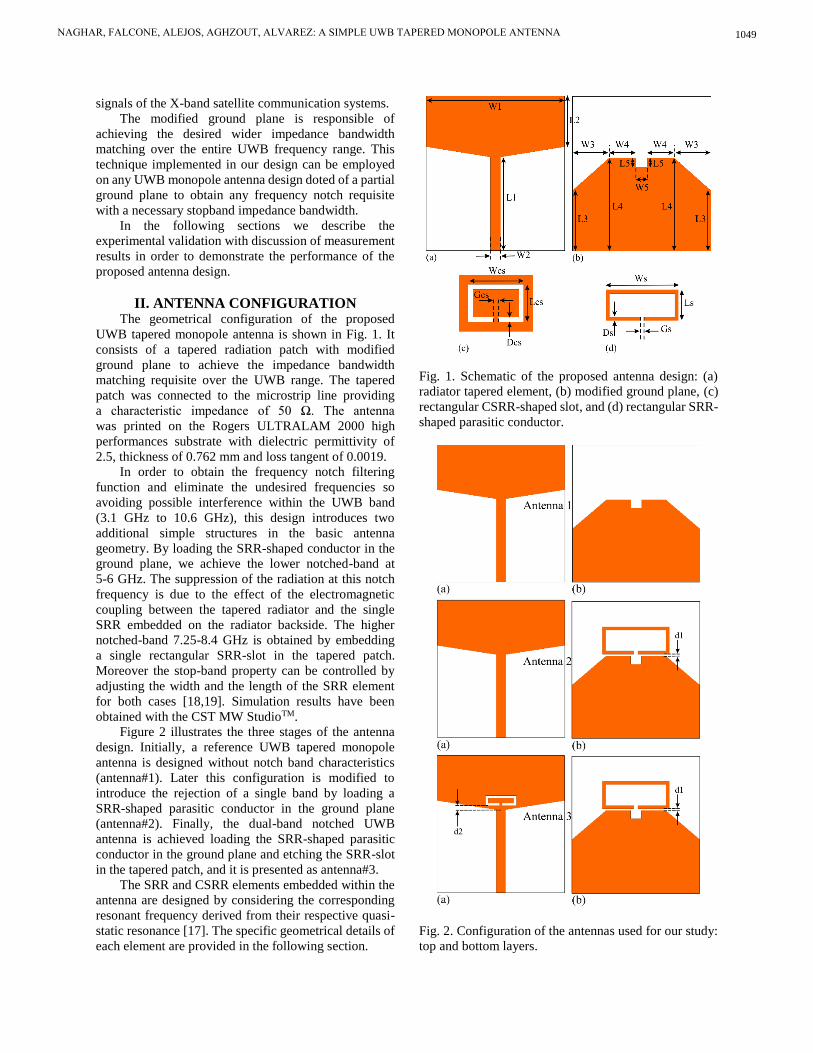
signals of the X-band satellite communication systems.
The modified ground plane is responsible of
achieving the desired wider impedance bandwidth
matching over the entire UWB frequency range. This
technique implemented in our design can be employed
on any UWB monopole antenna design doted of a partial
ground plane to obtain any frequency notch requisite
with a necessary stopband impedance bandwidth.
In the following sections we describe the
experimental validation with discussion of measurement
results in order to demonstrate the performance of the
proposed antenna design.
II. ANTENNA CONFIGURATIONThe geometrical configuration of the proposed
UWB tapered monopole antenna is shown in Fig. 1. It
consists of a tapered radiation patch with modified
ground plane to achieve the impedance bandwidth
matching requisite over the UWB range. The tapered
patch was connected to the microstrip line providing
a characteristic impedance of 50 Ω. The antenna
was printed on the Rogers ULTRALAM 2000 high
performances substrate with dielectric permittivity of
2.5, thickness of 0.762 mm and loss tangent of 0.0019.
In order to obtain the frequency notch filtering
function and eliminate the undesired frequencies so
avoiding possible interference within the UWB band
(3.1 GHz to 10.6 GHz), this design introduces two
additional simple structures in the basic antenna
geometry. By loading the SRR-shaped conductor in the
ground plane, we achieve the lower notched-band at
5-6 GHz. The suppression of the radiation at this notch
frequency is due to the effect of the electromagnetic
coupling between the tapered radiator and the single
SRR embedded on the radiator backside. The higher
notched-band 7.25-8.4 GHz is obtained by embedding
a single rectangular SRR-slot in the tapered patch.
Moreover the stop-band property can be controlled by
adjusting the width and the length of the SRR element
for both cases [18,19]. Simulation results have been
obtained with the CST MW StudioTM.
Figure 2 illustrates the three stages of the antenna
design. Initially, a reference UWB tapered monopole
antenna is designed without notch band characteristics
(antenna#1). Later this configuration is modified to
introduce the rejection of a single band by loading a
SRR-shaped parasitic conductor in the ground plane
(antenna#2). Finally, the dual-band notched UWB
antenna is achieved loading the SRR-shaped parasitic
conductor in the ground plane and etching the SRR-slot
in the tapered patch, and it is presented as antenna#3.
The SRR and CSRR elements embedded within the
antenna are designed by considering the corresponding
resonant frequency derived from their respective quasi-
static resonance [17]. The specific geometrical details of
each element are provided in the following section.
Fig. 1. Schematic of the proposed antenna design: (a)
radiator tapered element, (b) modified ground plane, (c)
rectangular CSRR-shaped slot, and (d) rectangular SRR-
shaped parasitic conductor.
Fig. 2. Configuration of the antennas used for our study:
top and bottom layers.
NAGHAR, FALCONE, ALEJOS, AGHZOUT, ALVAREZ: A SIMPLE UWB TAPERED MONOPOLE ANTENNA 1049

III. MEASUREMENT RESULTSFollowing we compare the performance of the three
stages of the antenna design: the reference design case
(antenna#1), single notched band case (antenna#2), and
the dual-band notched case (antenna#3).
A. UWB tapered monopole antenna
Figure 3 shows the VSWR performance of the basic
UWB tapered monopole antenna without any embedded
notch filtering element. As can be seen in the plot, the
UWB antenna operates from 2.8 to 12 GHz with a
voltage standing wave ratio (VSWR) lower than 2. Good
agreement between the measured and simulated plots is
inferred from the comparison. The parameters of the
UWB reference antenna without notch function are as
follows, in mm: L1=20, L2=10.8, L3=13, L4=20, L5=2,
W1=30, W2=2.2, W3=8, W4=6 and W5=2.5.
Fig. 3. Simulated and measured VSWR for antenna#1.
B. UWB tapered monopole antenna with single band-
notch
In order to reject the WLAN/DSRC frequencies
(5.05-5.95 GHz), we loaded a single SRR-shaped parasitic
on the backside of the tapered patch, so obtaining the
namely antenna#2 case. This notch filtering property is
due to the electromagnetic coupling occurring between
the radiating patch element and the resonant SRR-shaped
parasitic element. The selection of critical parameters of
the SRR structure is related to important effects arising
on the antenna performance.
Figure 4 shows the VSWR of antenna#2 obtained
for different values of the total length of the SRR-shaped
parasitic, given by Lt = Ls + Ws. It can be observed that
when the total length of the SRR structure increases, the
center of the notch frequency decreases without affecting
the stop-band impedance bandwidth. Then, the notch
frequency is controllable by varying the total length Lt of
the embedded SRR-shaped parasitic.
Furthermore, the band rejection is influenced by the
width of the SRR-shaped parasitic, Ds. This effect was
investigated and shown in Fig. 5. We observe that the
notched frequency depends of the SRR-shaped parasitic
width Ds, in a similar way to that one due to the influence
of the total length Lt, as previously described.
Fig. 4. Simulated VSWR for antenna#2 with different
values of Lt.
Fig. 5. Simulated VSWR of antenna#2 for different
values of Ds with Lt = 22.3 mm.
The capacitive coupling between the introduced
SRR-shaped parasitic and the modified ground plane
also affects the stop-band performance, as illustrated in
Fig. 6. We can deduce that the impedance bandwidth of
the stop-band increases as the distance d1 between the
ground plane and the SRR-shaped parasitic element
decreases. Rejection levels are enhanced when distance
d1 decreases, corresponding to an intensification in the
effective capacitive value provided by the gap between
the antenna and the SRR loading element [17]. Thus, the
variation of the distance d1 introduces an easy way for
ACES JOURNAL, Vol. 31, No.9, September 20161050

controlling both the stop-band impedance bandwidth and
the corresponding maximum value of VSWR.
The values of the design parameters selected for the
SRR-shaped parasitic conductor backed-plane are as
follows, in mm: Ws=15.7, Ls=6.6, Gs=0.8, Ds=0.8 and
d1=0.3.
Figure 7 shows comparison between the simulated
and measured VSWR characteristics of the single-band-
notched UWB antenna (antenna#2) and the reference
antenna (antenna#1). This plot clarifies that the achieved
notched frequency bandwidth is achieved from 5.05
to 5.95 GHz with a maximum VSWR higher than 10.
Obviously, the achieved notched bandwidth can suppress
the DSRC and WLAN bands for UWB communications.
Fig. 6. Simulated VSWR for antenna 2 with different
values of d1 (Lt = 22.3 mm, Ds = 0.8 mm).
Fig. 7. Simulated and measured VSWR of the proposed
UWB antenna with single frequency notch.
C. Dual band-notched UWB tapered monopole
antenna
The next step was to achieve a dual band notched
feature to reject the uplink and downlink signals of the
X-band satellite communications. Then, a SRR-slot was
etched in the tapered patch, as shown in Fig. 2, so
obtaining the namely antenna#3 case.
The proposed dual band-notched UWB antenna
with was fabricated and tested. The measured and
simulated VSWR of the antenna#3 are illustrated in
Fig. 8. It can be seen that for this case the impedance
bandwidth is 8.2 GHz, covering the band 2.8-11 GHz
along to achieving the required dual band-notched
performance. The simulated notched frequency
bandwidth of the proposed antenna is achieved from
4.95 GHz to 6.05 GHz and from 7.25 GHz to 8.45 GHz,
while the measured stop-band frequency ranges are from
4.95 GHz to 5.95 GHz and from 7.5 GHz to 8.9 GHz for
VSWR>2 with maximum VSWR of more than 10 and 4
respectively. The suppression of the WLAN/DSRC and
X-band narrow band systems was completely obtained.
The frequency shifting observed in the second frequency
notch of measurement results is due to the fabrication
tolerance limit when etching the SRR-slot.
Fig. 8. Simulated and measured VSWR of the proposed
dual bad-notched UWB antenna.
The design parameters of the etched SRR-slot are as
follows, in mm: Ws=7.2, Lcs=2.4, Gcs=0.6, Dcs=0.6 and
d2=1.
For the case of antenna#3, we analyzed the surface
current distribution. In Fig. 9, we depicted at two
frequencies of operation, (5.5 and 7.85 GHz, corresponding
to the center frequencies of the notched bands. It is
visible that the quasi-static resonance frequencies of the
SRR/CSRR elements are located precisely at 5.5 GHz
and 7.85 GHz. For those frequencies the tapered
monopole is then not excited and so resulting in the
radiation suppression.
The radiation pattern of the proposed antenna#3 is
presented in Fig. 10. The figure shows good directive
pattern in the E-plane and omnidirectional pattern for the
H-plane. General good agreement is observed between
measured and simulated results.
NAGHAR, FALCONE, ALEJOS, AGHZOUT, ALVAREZ: A SIMPLE UWB TAPERED MONOPOLE ANTENNA 1051

(a)
(b)
Fig. 9. Simulated surface current distribution of the dual
band-notched case (antenna#3): (a) at 5.5 GHz and (b) at
7.85 GHz.
(a)
(b)
(c)
Fig. 10. Simulated and measured radiation patterns of
the proposed antenna#3 case for E- and H-planes: (a)
4.5 GHz, (b) 6.5 GHz, and (c) 9.5 GHz.
In Fig. 11 we illustrate the variation of the peak gain
with the frequency for the single and dual frequency
notched antennas#2 and #3 over the frequency range (2-
12 GHz) along to the reference case (antenna#1). Sharp
dips in the value of the far-field peak gain are observed
in the two desired notched bands, confirming the fact that
loading the basic antenna with single SRR-shaped
parasitic and SRR-slot provides excellent intrinsic notch
filtering.
Furthermore, it can be checked that, in the radiating
band, the gain variation is almost the same for the three
antennas. Photographs of fabricated antenna prototypes
are shown in Fig. 12.
Fig. 11. Peak gain for the three cases of UWB tapered
antennas.
(a)
(b)
Fig. 12. Photograph of prototyped antennas: (a) top later
and (b) bottom layer. Left: Antenna1. Center: Antenna 2.
Right: Antenna 3.
ACES JOURNAL, Vol. 31, No.9, September 20161052

VI. CONCLUSIONA simple and symmetric tapered monopole UWB
antenna with a single SRR-shaped parasitic and single
SRR-slot etched in the tapered patch, exhibiting dual-
frequency notch performance is presented in this paper.
The electromagnetic coupling between the tapered patch
and the SRR-shaped parasitic introduced on the back side
of the tapered element, yields the first notch at 5.5 GHz,
with a large bandwidth, filtering the interferences due to
the co-existence of DSRC/WLAN systems. Moreover,
the uplink and downlink signals of the X-band satellite
communication systems are rejected by embedding a
single SRR-slot on the radiation patch. The notched
frequencies can be easy controlled by modifying the
dimensions of the SRR structures. Fabricated antennas
demonstrate overall good match between simulated and
measured results. In summary, a simple design procedure,
valid to obtain a good omnidirectional radiation pattern,
with relative stable gain and low profile, as well as
manufacturable at low cost make the proposed antenna a
suitable candidate for UWB systems needed of multiple
frequencies notches.
ACKNOWLEDGMENT The authors would like to thank the support given
under projects EMR2012/138 and GRC1015/019 funded
by Xunta de Galicia, and Erasmus Mundus Green IT
(Grant 2012-2625/001-001-EMA2).
REFERENCES [1] Federal Communications Commission, “Federal
Communications Commission revision of Part 15
of the commission’s rules regarding ultra-wideband
transmission system from 3.1 to 10.6 GHz,”
Washington, DC, USA, 2002.
[2] M. Rostamzadeh, S. Mohamadi, J. Nourinia, C.
Ghobadi, and M. Ojaroudi, “Square monopole
antenna for UWB applications with novel rod-
shaped parasitic structures and novel V-shaped
slots in the ground plane,” IEEE Antennas and
Wireless Propagation Letters, vol. 11, pp. 446-449,
2012.
[3] N.-I. Jo, C.-Y. Kim, D.-O. Kim, and H.-A. Jang,
“Compact ultrawideband antenna with quadruple-
band rejection characteristics using SRR/CSRR
structure,” Journal of Electromagnetic Waves and
Applications, vol. 26, no. 5-6, pp. 583-592, 2012.
[4] M. Rostamzadeh, S. Mohamadi, J. Nourinia, C.
Ghobadi, and M. Ojaroudi, “Square monopole
antenna for UWB applications with novel rod-
shaped parasitic structures and novel V-shaped
slots in the ground plane,” IEEE Antennas and
Wireless Propagation Letters, vol. 11, pp. 446-449,
2012.
[5] K. G. Thomas and M. A. Sreenivasan, “A simple
ultrawideband planar rectangular printed antenna
with band dispensation,” IEEE Transactions on
Antennas and Propagation, vol. 58, no. 1, pp. 27-
34, 2010.
[6] R. Azim, M. T. Islam, J. S. Mandeep, and A. T.
Mobashsher, “A planar circular ring ultra-wideband
antenna with dual bandnotched characteristics,”
Journal of Electromagnetic Waves and Applications,
vol. 26, no. 14-15, pp. 2022-2032, 2012.
[7] S. Mohammadi, J. Nourinia, C. Ghobadi, and M.
Majidzadeh, “Compact CPW-fed rotated square-
shaped patch slot antenna with band-notched
function for UWB applications,” Electronics Letters,
vol. 47, no. 24, pp. 1307-1308, 2011.
[8] H.-W. Liu, C.-H. Ku, T.-S. Wang, and C.-F. Yang,
“Compact monopole antenna with band-notched
characteristic for UWB applications,” IEEE
Antennas and Wireless Propagation Letters, vol. 9,
pp. 397-400, 2010.
[9] M. C. Tang, et al., “Compact UWB antenna with
multiple band-notches for WiMAX and WLAN,”
IEEE Trans. Antennas Propagation, vol. 59, no. 4,
pp. 1372-1376, Apr. 2001.
[10] J. Y. Siddiqui, C. Saha, and Y. M. M. Antar,
“Compact dual-SRR-loaded UWB monopole
antenna with dual frequency and wideband notch
characteristics,” IEEE Antennas and Wireless
Propagation Letters, vol. 14, pp. 100-103, 2015.
[11] D. Sarkar, K. V. Srivastava, and K. Saurav, “A
compact microstrip-fed triple band-notched ultra-
wideband monopole antenna,” IEEE Antennas and
Wireless Propagation Letters, vol. 13, pp. 396-399,
2014.
[12] M. S. A. Rani, S. K. A. Rahim, M. R. Kamarudin,
T. Peter, S. W. Cheung, and B. M. Saad,
“Electromagnetic behaviors of thin film CPW-fed
CSRR loaded on UWB transparent antenna,” IEEE
Antennas and Wireless Propagation Letters, vol.
13, pp. 1239-1242, 2014.
[13] M. M. Islam, M. R. I. Faruque, and M. T. Islam, “A
compact 5.5 GHz band-rejected UWB antenna
using complementary split ring resonators,” The
Scientific World Journal, vol. 2014.
[14] Q. Wang and Y. Zhang, “Design of a compact
UWB antenna with triple band-notched
characteristics,” International Journal of Antennas
and Propagation, vol. 2014.
[15] M. C. Tang, “Compact UWB antenna with multiple
band-notches for WiMAX and WLAN,” IEEE
Trans. Antennas Propagation, vol. 59, no. 4, pp.
1372-1376, 2001.
[16] T. Yuan, C.-W. Qiu, L. W. Li, M. S. Leong, and Q.
Zhang, “Elliptically shaped ultra-wideband patch
antenna with band-notch features,” Microw. Opt.
Tech. Lett., vol. 50, no. 3, pp. 736-738, 2008.
[17] J. Baena, J. Bonache, F. Martín, R. Marqués, F.
Falcone, T. Lopetegi, M. Laso, J. Gil, M. Flores,
NAGHAR, FALCONE, ALEJOS, AGHZOUT, ALVAREZ: A SIMPLE UWB TAPERED MONOPOLE ANTENNA 1053
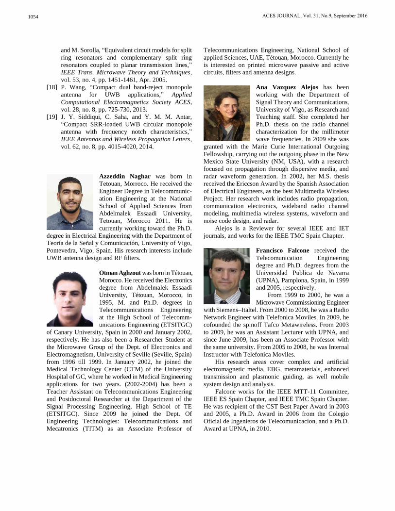
and M. Sorolla, “Equivalent circuit models for split
ring resonators and complementary split ring
resonators coupled to planar transmission lines,”
IEEE Trans. Microwave Theory and Techniques,
vol. 53, no. 4, pp. 1451-1461, Apr. 2005.
[18] P. Wang, “Compact dual band-reject monopole
antenna for UWB applications,” Applied
Computational Electromagnetics Society ACES,
vol. 28, no. 8, pp. 725-730, 2013.
[19] J. Y. Siddiqui, C. Saha, and Y. M. M. Antar,
“Compact SRR-loaded UWB circular monopole
antenna with frequency notch characteristics,”
IEEE Antennas and Wireless Propagation Letters,
vol. 62, no. 8, pp. 4015-4020, 2014.
Azzeddin Naghar was born in
Tetouan, Morroco. He received the
Engineer Degree in Telecommunic-
ation Engineering at the National
School of Applied Sciences from
Abdelmalek Essaadi University,
Tetouan, Morocco 2011. He is
currently working toward the Ph.D.
degree in Electrical Engineering with the Department of
Teoría de la Señal y Comunicación, University of Vigo,
Pontevedra, Vigo, Spain. His research interests include
UWB antenna design and RF filters.
Otman Aghzout was born in Tétouan,
Morocco. He received the Electronics
degree from Abdelmalek Essaadi
University, Tétouan, Morocco, in
1995, M. and Ph.D. degrees in
Telecommunications Engineering
at the High School of Telecomm-
unications Engineering (ETSITGC)
of Canary University, Spain in 2000 and January 2002,
respectively. He has also been a Researcher Student at
the Microwave Group of the Dept. of Electronics and
Electromagnetism, University of Seville (Seville, Spain)
from 1996 till 1999. In January 2002, he joined the
Medical Technology Center (CTM) of the University
Hospital of GC, where he worked in Medical Engineering
applications for two years. (2002-2004) has been a
Teacher Assistant on Telecommunications Engineering
and Postdoctoral Researcher at the Department of the
Signal Processing Engineering, High School of TE
(ETSITGC). Since 2009 he joined the Dept. Of
Engineering Technologies: Telecommunications and
Mecatronics (TITM) as an Associate Professor of
Telecommunications Engineering, National School of
applied Sciences, UAE, Tétouan, Morocco. Currently he
is interested on printed microwave passive and active
circuits, filters and antenna designs.
Ana Vazquez Alejos has been
working with the Department of
Signal Theory and Communications,
University of Vigo, as Research and
Teaching staff. She completed her
Ph.D. thesis on the radio channel
characterization for the millimeter
wave frequencies. In 2009 she was
granted with the Marie Curie International Outgoing
Fellowship, carrying out the outgoing phase in the New
Mexico State University (NM, USA), with a research
focused on propagation through dispersive media, and
radar waveform generation. In 2002, her M.S. thesis
received the Ericcson Award by the Spanish Association
of Electrical Engineers, as the best Multimedia Wireless
Project. Her research work includes radio propagation,
communication electronics, wideband radio channel
modeling, multimedia wireless systems, waveform and
noise code design, and radar.
Alejos is a Reviewer for several IEEE and IET
journals, and works for the IEEE TMC Spain Chapter.
Francisco Falcone received the
Telecomunication Engineering
degree and Ph.D. degrees from the
Universidad Publica de Navarra
(UPNA), Pamplona, Spain, in 1999
and 2005, respectively.
From 1999 to 2000, he was a
Microwave Commissioning Engineer
with Siemens–Italtel. From 2000 to 2008, he was a Radio
Network Engineer with Telefonica Moviles. In 2009, he
cofounded the spinoff Tafco Metawireless. From 2003
to 2009, he was an Assistant Lecturer with UPNA, and
since June 2009, has been an Associate Professor with
the same university. From 2005 to 2008, he was Internal
Instructor with Telefonica Moviles.
His research areas cover complex and artificial
electromagnetic media, EBG, metamaterials, enhanced
transmission and plasmonic guiding, as well mobile
system design and analysis.
Falcone works for the IEEE MTT-11 Committee,
IEEE ES Spain Chapter, and IEEE TMC Spain Chapter.
He was recipient of the CST Best Paper Award in 2003
and 2005, a Ph.D. Award in 2006 from the Colegio
Oficial de Ingenieros de Telecomunicacion, and a Ph.D.
Award at UPNA, in 2010.
ACES JOURNAL, Vol. 31, No.9, September 20161054
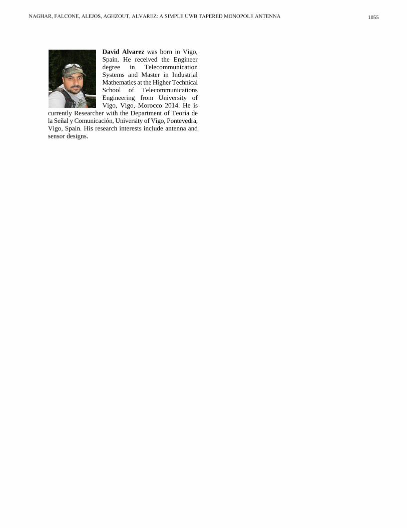
David Alvarez was born in Vigo,
Spain. He received the Engineer
degree in Telecommunication
Systems and Master in Industrial
Mathematics at the Higher Technical
School of Telecommunications
Engineering from University of
Vigo, Vigo, Morocco 2014. He is
currently Researcher with the Department of Teoría de
la Señal y Comunicación, University of Vigo, Pontevedra,
Vigo, Spain. His research interests include antenna and
sensor designs.
NAGHAR, FALCONE, ALEJOS, AGHZOUT, ALVAREZ: A SIMPLE UWB TAPERED MONOPOLE ANTENNA 1055

Synthesis Design of Bandpass Filter for UWB Applications with Improved
Selectivity
Azzeddin Naghar 1,2, Otman Aghzout 2, Ana V. Alejos 1, and Francisco Falcone 3
1 Department of Teoría de la Señal y Comunicación
University of Vigo, Vigo, 36310, Spain
[email protected], [email protected]
2 Department of TTIM
Abdelmalek Essaadi University, Tetouan, Morocco
3 Department of Ingeniería Electrical y Electrónica
University of Navarra, Pamplona, Spain
Abstract This paper presents the design of UWB three-
pole modified parallel coupled line bandpass filter with
improved rejection in the out-of-band frequencies. To
achieve the desired UWB requirements using the
conventional bandpass filter design, a physical dimension
optimization of space-gap between lines, line widths and
lengths was applied. An equivalent circuit model is also
presented and demonstrates reasonable agreement with
simulation results. The optimized filter demonstrates an
excellent UWB performance, covering the Federal
Communication Commission spectrum bandwidth with
low insertion loss and acceptable selectivity. However,
this resulting filter structure presents very small gapping
between adjacent resonators; that means the filter is
unmanufactured. Then an example of an alternative filter
structure is finally proposed with null gaping and short-
circuited stubs that yields to a fabricated prototype with
selectivity improvement. Generally speaking, reasonable
agreement is achieved between measurement and
simulation results.
Index Terms Bandpass filter, coupling gap, parallel
coupled line, rejection band, stub, UWB.
I. INTRODUCTION
The ultra-wideband (UWB) radio technology has
been getting increasingly popular due to the high-speed
high-data wireless connectivity demand. There is a need
to design ultra-wideband bandpass filters covering the
whole band permitted by the U.S. Federal Communication
Commission (FCC), that extends from 3.1 to 10.6 GHz
[1]. The design requirements of these circuits face new
challenges among which are included an overall good
performance, compact size, wide bandwidth feature and
multi-band operation. Various approaches to implement
UWB filters can be found through literature [2-4].
Among other microstrip line centered configurations,
bandpass filters based on parallel-coupled lines have
been widely used in microwave systems, due to their
good performance, simple structure, low cost and ease of
integration with other devices [5-6].
This paper presents the design of a three-pole
parallel coupled lines microstrip bandpass filter (BPF)
for UWB applications. The filter design was accomplished
in three steps. Firstly, a filter is designed and optimized
to cover the FCC band.
The physical parameter dimensions for this initial
design are calculated by an ad-hoc tool [6] and then
optimized in a second design step to achieve a better
UWB performance. However, this resulting filter cannot
be fabricated due to the small spacing between adjacent
coupled lines.
To solve this limitation, a modified filter structure is
proposed in a third design step, by null gapping the space
between all the filter parallel resonators, and incorporating
short circuited stubs. This final design is manufactured
and offers selectivity enhancement, covering the FCC
spectrum with lower insertion loss and group velocity
flatness, along with elimination of the transmission at
low frequency. It also presents a size reduction, and it
can be implemented on low cost dielectric substrate of
FR4.
II. UWB BANDPASS FILTER: DESIGN AND
RESULTS
A. Edge-coupled bandpass filter for UWB applications
According to [7,8,9], the edge-coupled bandpass
three-order filter is designed to cover the FCC full band,
with center frequency of 6.85 GHz, and passband ripple
of 0.5. The filter has been implemented on FR4 substrate
with dielectric constant of 4.4 and thickness of 1.6 mm.
As a first step, we define the initial physical dimension
1054-4887 © 2016 ACES
Submitted On: January 1, 2015Accepted On: December 6, 2015
8 ACES JOURNAL, Vol. 31, No. 1, January 2016
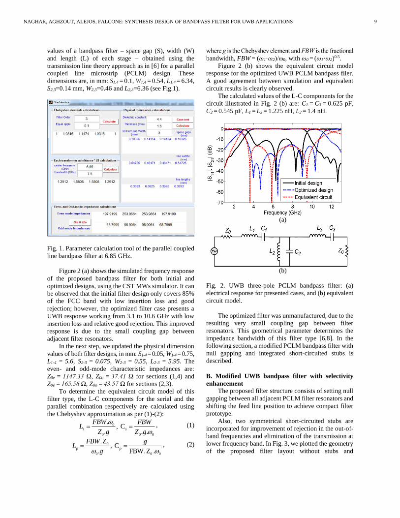
values of a bandpass filter – space gap (S), width (W)
and length (L) of each stage – obtained using the
transmission line theory approach as in [6] for a parallel
coupled line microstrip (PCLM) design. These
dimensions are, in mm: S1,4 = 0.1, W1,4 = 0.54, L1,4 = 6.34,
S2,3=0.14 mm, W2,3=0.46 and L2,3=6.36 (see Fig.1).
Fig. 1. Parameter calculation tool of the parallel coupled
line bandpass filter at 6.85 GHz.
Figure 2 (a) shows the simulated frequency response
of the proposed bandpass filter for both initial and
optimized designs, using the CST MWs simulator. It can
be observed that the initial filter design only covers 85%
of the FCC band with low insertion loss and good
rejection; however, the optimized filter case presents a
UWB response working from 3.1 to 10.6 GHz with low
insertion loss and relative good rejection. This improved
response is due to the small coupling gap between
adjacent filter resonators.
In the next step, we updated the physical dimension
values of both filter designs, in mm: S1-4 = 0.05, W1-4 = 0.75,
L1-4 = 5.6, S2-3 = 0.075, W2-3 = 0.55, L2-3 = 5.95. The
even- and odd-mode characteristic impedances are:
Z0e = 1147.33 Ω, Z0o = 37.41 Ω for sections (1,4) and
Z0e = 165.56 Ω, Z0o = 43.57 Ω for sections (2,3).
To determine the equivalent circuit model of this
filter type, the L-C components for the serial and the
parallel combination respectively are calculated using
the Chebyshev approximation as per (1)-(2):
0
0 0 0
., C
. . .s s
FBW FBWL
Z g Z g
, (1)
0
0 0 0
.Z, C
. FBW.Z .p p
FBW gL
g , (2)
where g is the Chebyshev element and FBW is the fractional
bandwidth, FBW = (ω1·ω2)/ω0, with ω0 = (ω1·ω2)0.5.
Figure 2 (b) shows the equivalent circuit model
response for the optimized UWB PCLM bandpass filer.
A good agreement between simulation and equivalent
circuit results is clearly observed.
The calculated values of the L-C components for the
circuit illustrated in Fig. 2 (b) are: C1 = C3 = 0.625 pF,
C2 = 0.545 pF, L1 = L3 = 1.225 nH, L2 = 1.4 nH.
(a)
(b)
Fig. 2. UWB three-pole PCLM bandpass filter: (a)
electrical response for presented cases, and (b) equivalent
circuit model.
The optimized filter was unmanufactured, due to the
resulting very small coupling gap between filter
resonators. This geometrical parameter determines the
impedance bandwidth of this filter type [6,8]. In the
following section, a modified PCLM bandpass filter with
null gapping and integrated short-circuited stubs is
described.
B. Modified UWB bandpass filter with selectivity
enhancement
The proposed filter structure consists of setting null
gapping between all adjacent PCLM filter resonators and
shifting the feed line position to achieve compact filter
prototype.
Also, two symmetrical short-circuited stubs are
incorporated for improvement of rejection in the out-of-
band frequencies and elimination of the transmission at
lower frequency band. In Fig. 3, we plotted the geometry
of the proposed filter layout without stubs and
NAGHAR, AGHZOUT, ALEJOS, FALCONE: SYNTHESIS DESIGN OF BANDPASS FILTER FOR UWB APPLICATIONS 9

photograph of the fabricated prototype. The physical
dimension values of this filter are, in mm: W1 = W4 = 1.42,
L1 = L4 = 5.8, W2 = W3 = 0.7 and L2 = L3 = 6.
This prototype was measured using a N5222A
Agilent Network Analyser. The simulated and measured
return loss and insertion of this filter design is plotted in
Fig. 4. We note that the fabricated UWB bandpass filter
demonstrates a low insertion loss within the FFC band.
However, a poor out-of-band rejection performances is
seen, due to the small gaps applied between PCLM
resonators. Then an enhancement of filter selectivity is
necessary.
(a)
(b)
Fig. 3. Modified UWB bandpass filter without stubs: (a)
filter layout, and (b) photograph of fabricated prototype.
Fig. 4. Electrical response of the modified UWB bandpass
filter without stubs.
To solve the limitation of poor selectivity, we added
two symmetrical short-circuited as shown in Fig. 5 (a),
in order to create the desired rejection and eliminate the
transmission at low frequency.
The photograph of the fabricated final filter
prototype is shown in Fig. 5 (b). For this design, the
length and width of the stubs determine the center
frequency and bandwidth of the rejected band. Whereas,
the rejection level is controlled by the stub positioning
parameter, D.
Figure 6 (a) shows the insertion loss of the final
modified filter design, with respect to the previous
proposed filter cases. The comparison indicates that the
modified bandpass filter presents a wider impedance
bandwidth, lower insertion loss and improved selectivity.
The integrated symmetrical stubs offer a rejection peak
at 12.5 GHz (-40 dB). A good agreement is achieved
between measurements and simulation.
By comparing to the conventional optimized filter
previously presented, the modified filter offers an
enhancement in the UWB impedance bandwidth (5%)
with improved selectivity. However, it presents a small
increase of the insertion loss (about 1.5 dB), due to the
integration of the stubs.
Finally, we plotted in Fig. 7, the simulated group
delay for the initial, the optimized and the modified filter
designs. Within the UWB passband, both of conventional
and modified bandpass filters demonstrate flat values
(<0.2 ns) of group delay, that meet the requirements
established by the FCC regulations for the UWB devices.
(a)
(b)
Fig. 5. Modified UWB bandpass filter with stubs: (a)
filter layout, and (b) photograph of fabricated prototype.
10 ACES JOURNAL, Vol. 31, No. 1, January 2016

(a)
(b)
Fig. 6. (a) Insertion loss of the UWB bandpass filter for
all proposed cases. (b) Schematic of distributed elements
corresponding to the filter design with stubs.
Fig. 7. Parameter calculation tool of the parallel coupled
line bandpass filter at 6.85 GHz.
C. Results discussion
Based on the conformal mapping method reported
in [10], the even- and odd-mode characteristic impedances
of the coupled line depend on the width W and coupling
gap S of one stage parallel coupled line. When the
dielectric constant εr and thickness h of the substrate are
known, the impedances Z0e and Z0o can be calculated as
a function of the strip line width and coupling gap for
each stage of parallel coupled lines of the filter. Then by
decreasing the coupling gap S values, the Z0e values
increase, Z0o decrease and consequently the bandwidth
of the parallel coupled line bandpass filter increases.
Detailed analysis and corresponding graphs of the even-
and odd-mode impedances are depicted in [12].
Using the closed formulas developed by Hammerstad,
Kirschning and Jansen for modelling the frequency-
dependency of the even- and odd-mode characteristics of
a parallel coupled microstrip line [10,11]. The variation
of the static characteristic impedances for even- and odd-
modes is calculated easily, as well as the fractional
bandwidth (FBW) variation of the PCLM filter type.
Calculated FBWs in (%), for different values of the
coupling gaps S1-4 and S2-3 are presented in Table 1. This
FBW is obtained by determining the ABCD matrix and
S-parameters as indicated in [13], based on the design
specification presented previously. The three-pole parallel
coupled line microstrip bandpass filter implements the
FR4 substrate with center frequency of 6.85 GHz and
passband ripple of 0.5.
However, this filter configuration with very small
coupling gap kept unmanufactured. Then we modified
our design by setting null spacing between filter
resonators. This resulting structure offers a relative poor
selectivity which can be improved using several
techniques, such as the short-circuited stubs here
described. This latter allows eliminating the lower band
frequency transmission.
The resonance frequency of the stub is given by (3):
0.52. .( )
stub
re
cf
L , (3)
where L is the total length of the slot, εre is the effective
dielectric constant and c is the speed of light. The
dimensions of the short-circuited stubs here used are:
Lsl = 6.5 mm, Wsl = 0.4 mm and D = 4.6 mm.
Table 1: Variation of the calculated FBW in percentage
with the small coupling gap values
Gapping
(S1-4, S2-3)
Z0e
(1-4, 2-3)
Z0o
(1-4, 2-3) FBW %
III. CONCLUSION In this paper a modified parallel coupled line
microstrip bandpass filter for UWB application is
presented. Based on a classical design of the parallel
coupled line microstrip filters, an UWB bandpass filter
is firstly introduced and discussed. Later an optimized
design is obtained demonstrating an improved performance
with respect to the FCC requirements for UWB devices.
A low insertion loss with relative good rejection was
obtained within the FCC passband. The equivalent
circuit model was also calculated and good agreement is
seen with simulation. However, the filter presents very
NAGHAR, AGHZOUT, ALEJOS, FALCONE: SYNTHESIS DESIGN OF BANDPASS FILTER FOR UWB APPLICATIONS 11

small gap values so demanding a high accuracy in the
manufacturing process not achievable for our capabilities.
A limit case is proposed with null gapping to yield a
fabricated prototype. The short-circuited stubs are
integrated to improve the filter selectivity and eliminate
the transmission at low frequency. Measurements results
demonstrate the validity of the design method proposed
in this paper, achieving an improved performance in
terms of UWB bandwidth, low insertion loss and good
rejection band without increasing the complexity of the
filter structure.
The proposed technique is a good candidate for
UWB bandpass filter design, and it can be generally
applied to obtain UWB bandpass filters for any
specifications.
This work can be extended to achieve a wider
rejection in the out-of-band frequencies regardless the
used selectivity enhancement technique. As an example,
an array of stubs with multiple close resonances.
As set-off, the filter width dimension has grown, and
as possible solution to this disadvantage we propose the
design of the stub in meander shape. A solution as
replacing stubs by stub-slots in the input feedline would
affect the S21 parameter introducing a larger insertion
loss. Despite the disadvantage of the increasing width
dimension, the short-circuited stub is a solution valid to
jointly achieve an improved selectivity and the elimination
of the low-frequency transmission.
ACKNOWLEDGMENT Research supported by the Xunta de Galicia (Grant
EMR2012/238) and Erasmus Mundus Green IT (Grant
2012-2625/001-001-EMA2).
REFERENCES [1] Federal Communications Commission, “First report
and order in the matter of revision of Part 15 of
the commission’s rules regarding ultrawideband
transmission systems,” Tech Report, ET-Docket
98-153, FCC02-48, Apr. 2002.
[2] X. Li and X. Ji, “Novel compact UWB bandpass
filters design with cross-coupling between λ/4
short-circuited stubs,” IEEE Microw. Wireless
Compon. Lett., vol. 24, no. 1, pp. 23-25, Jan. 2014.
[3] H. Shaman and J. S. Hong, “A novel ultra-
wideband (UWB) bandpass filter (BPF) with pairs
of transmission zeroes,” IEEE Microw. Wireless
Compon. Lett., vol. 17, no. 2, pp. 121-123, Feb.
2007.
[4] Z.-X. Zhang and F. Xiao, “An UWB bandpass
filter based on a novel type of multi-mode
resonator,” IEEE Microw. Wireless Compon. Lett.,
vol. 22, no. 10, pp. 506-508, Oct. 2012.
[5] P. Cai, Z. Ma, X. Guan, Y. Kobayashi, T. Anada,
and G. Hagiwara, “Synthesis and realization of
novel ultra-wideband bandpass filters using 3/4
wavelength parallel-coupled line resonators,”
Asia-Pacific Microwave Conference, Yokohama,
Japan, pp. 159-162, Dec. 2006.
[6] A. Naghar, O. Aghzout, A. Vazquez Alejos, M.
Garcıa Sanchez, and M. Essaaidi, “Design of
compact wideband multi-band and ultrawideband
band pass filters based on coupled half wave
resonators with reduced coupling gap,” IET
Microwave, Antennas and Propagation, pp. 1-7,
2015.
[7] A. Naghar, O. Aghzout, A. Vazquez Alejos, M.
Garcıa Sanchez, and M. Essaaidi, “Development of
a calculator for edge and parallel coupled
microstrip band pass filters,” IEEE International
Symposium on Antennas and Propagation, Memphis,
USA, pp. 2018-2019, Jul. 2014.
[8] A. Naghar, O. Aghzout, A. Vazquez Alejos, M.
Garcıa Sanchez, and M. Essaaidi, “Design of
compact multi-band bandpass filter with suppression
of second harmonic spurious by coupling gap
reduction,” Journal of Electromagnetic Waves and
Applications, vol. 29, no. 14, pp. 1813-1828, Aug.
2015.
[9] S. Akhtarzad, T. R. Rowbotham, and P. B. Johns,
“The design of coupled microstrip lines,” IEEE
Transactions on Microwave Theory and Techniques,
vol. MTT-23, no. 6, pp. 486-492, Jun. 1975.
[10] E. Hammerstad and O. Jensen, “Accurate models
for microstrip computer-aided design,” Symposium
on Microwave Theory and Techniques, pp. 407-
409, Jun. 1980.
[11] M. Kirschning and R. H. Jansen, “Accurate wide-
range design equations for the frequency dependent
characteristic of parallel coupled microstrip lines,”
IEEE Trans. Microwave Theory Tech., vol. MTT-
32, no. 1, pp. 83-90, Jan. 1984.
[12] C. S. Ye, Y. K. Su, M. H. Weng, C. Y. Hung, and
R. Y. Yang, “Design of the compact parallel-coupled
lines wideband bandpass filters using image
parameter method,” Progress In Electromagnetics
Research, vol. 100, pp. 153-173, 2010.
[13] K.-S. Chin, Y.-C. Chiou, and J.-T. Kuo, “New
synthesis of parallel-coupled line bandpass filters
with Chebyshev responses,” IEEE Trans. Microwave
Theory Tech., vol. 56, no. 7, pp. 1516-1523, Jul.
2008.
Azzedin Naghar was born in
Tetouan, Morroco. He received the
Engineer degree in Telecommunication
Engineering at the National School of
Applied Sciences from Abdelmalek
Essaadi University, Tetouan, Morocco
in 2011. He is currently working
toward the Ph.D. degree in Electrical
12 ACES JOURNAL, Vol. 31, No. 1, January 2016
Engineering with the Department of Teoría de la Señal y
comunicación, University of Vigo, Pontevedra, Vigo,
Spain. His research interests include UWB antenna
design and RF filters.
Otman Aghzout was born in
Tétouan, Morocco. He received the
Electronics degree from Abdelmalek
Essaadi University, Tétouan,
Morocco, in 1995, the M. and the
Ph.D. degrees in Telecommunications
Engineering at the High School of
Telecommunications Engineering
(ETSITGC) of Canary University, Spain in 2000 and
January 2002, respectively. He has also been a
Researcher Student at the Microwave Group of the Dept.
of Electronics and Electromagnetism, University of
Seville (Seville, Spain) from 1996 till 1999. In January
2002, he joined the Medical Technology Center (CTM)
of the University Hospital of GC, where he worked in
Medical Engineering applications for two years. From
2002-2004 he has been a Teacher Assistant on
Telecommunications Engineering and Postdoctoral
Researcher at the Department of the Signal Processing
Engineering, High School of TE (ETSITGC). Since 2009
he joined the Dept. of Engineering Technologies:
Telecommunications and Mecatronics (TITM) as an
Associate Professor of Telecommunications Engineering,
National School of Applied Sciences, UAE, Tétouan,
Morocco. Currently he is interested on printed microwave
passive and active circuits, filters and antenna designs.
Ana Vazquez Alejos has been
working with the Department of
Signal Theory and Communications,
University of Vigo, as Research and
Teaching Staff. She completed her
Ph.D. thesis on the radio channel
characterization for the millimeter
wave frequencies. In 2009 she was
granted with the Marie Curie International Outgoing
Fellowship, carrying out the outgoing phase in the New
Mexico State University (NM, USA), with a research
focused on propagation through dispersive media, and
radar waveform generation. In 2002, her M.S. thesis
received the Ericcson Award by the Spanish Association
of Electrical Engineers, as the best Multimedia Wireless
Project. Her research work includes radio propagation,
communication electronics, wideband radio channel
modeling, multimedia wireless systems, waveform and
noise code design, and radar.
Alejos is a Reviewer for several IEEE and IET
Journals, and works for the IEEE TMC Spain Chapter.
Francisco Falcone received the
Telecommunication Engineering
degree and Ph.D. degrees from the
Universidad Publica de Navarra
(UPNA), Pamplona, Spain, in 1999
and 2005, respectively.
From 1999 to 2000, he was a
Microwave Commissioning Engineer
with Siemens–Italtel. From 2000 to 2008, he was a Radio
Network Engineer with Telefonica Moviles. In 2009, he
cofounded the spinoff Tafco Metawireless. From 2003
to 2009, he was an Assistant Lecturer with UPNA, and
since June 2009, has been an Associate Professor with
the same university. From 2005 to 2008, he was Internal
Instructor with Telefonica Moviles.
His research areas cover complex and artificial
electromagnetic media, EBG, metamaterials, enhanced
transmission and plasmonic guiding, as well mobile
system design and analysis.
Falcone works for the IEEE MTT-11 committee,
IEEE ES Spain Chapter, and IEEE TMC Spain Chapter.
He was recipient of the CST Best Paper award in 2003
and 2005, a Ph.D. award in 2006 from the Colegio
Oficial de Ingenieros de Telecomunicacion, and a Ph.D.
award at UPNA, in 2010.
NAGHAR, AGHZOUT, ALEJOS, FALCONE: SYNTHESIS DESIGN OF BANDPASS FILTER FOR UWB APPLICATIONS 13

Design of compact wideband multi-band andultrawideband band pass filters based oncoupled half wave resonators with reducedcoupling gap
ISSN 1751-8725Received on 30th July 2014Revised on 27th May 2015Accepted on 2nd August 2015doi: 10.1049/iet-map.2015.0188www.ietdl.org
Azzedin Naghar1,2, Otman Aghzout3, Ana Vazquez Alejos1 , Manuel Garcia Sanchez1,
Mohamed Essaaidi4
1Department of Teoría de la Señal y comunicación, University of Vigo, Pontevedra, Vigo, Spain2Department of Physics, Faculty of Sciences, Abdelmalek Essaadi University, Tetouan, Morocco3Department TITM, National School of Applied Sciences, Abdelmalek Essaadi University, Tetouan, Morocco4Department of ENSIAS, University of Mohamed V-Souissi, Rabat, Morocco
E-mail: [email protected]
Abstract: In this paper we propose a technique to design compact multi-band and UWB bandpass filters based on coupledhalf wave resonators. The proposed design consists of the modification of a conventional parallel coupled Chebyshevbandpass filter structure by setting a very small or null coupling gap between the resonators of the center sectionsjointly with a very small spacing between resonators of the extremity sections. This spacing determines theperformances of selected frequency bands. An ultrawideband response is accomplished by applying null spacingbetween all the adjacent resonators. We analysed the effect of the separation distance between the coupled lines onboth the fractional bandwidth and group velocity of the filter response. The effect of the order assumed for the initialChebyshev filter was also discussed. As an illustration of the proposed technique, we designed and measured a dualband and a tri-band filter for the frequencies covering the WiMAX/WLAN/X system bands demonstrating an excellentperformance, with a fractional bandwidth covering the 40% and 100% of the FCC bandwidth respectively. Theproposed technique alleviates the fabrication accuracy requirements. The designs show an optimal improvement interms of group velocity flatness.
1 Introduction
With the rapid development of wireless communications in recentyears, a demand for passive circuits has quickly increased, such asbandpass filters (BPFs). Multi-band (MB) and ultrawideband(UWB) operation is common target for today’s wirelesscommunication systems, and then balanced BPFs are highlydesired for such systems. The design requirements of these circuitsface new challenges among which are included an overall goodperformance, wide bandwidth operation feature, high frequencyselectivity, compact size and the use of a microstrip lineconfiguration. There are also standardised requirements to beaccomplished in the design of an UWB band pass filter coveringthe frequency band defined by the U.S. Federal CommunicationCommission (FCC) that extends from 3.1 to 10.6 GHz [1]. Amongthese requirements we can mention: meet the FCC spectrum muskregulation; low insertion loss (<0.5 dB); low ripples (<0.5 dB);mild group delay variation (<0.2 ns); transmission zeros above andbelow the passband which means good attenuation slopes of theskirts selectivity [2, 3].
Various approaches to implement MB and UWB filters have beendesigned and analysed through literature [4–9]. Among othermicrostrip line centred configurations, BPFs based onparallel-coupled stepped-impedance resonators (SIRs) have beenwidely used in microwave systems, due to their good performance,simple structure, low cost and ease of integration with otherdevices. A general layout of a parallel coupled microstrip BPF isshown in Fig. 1. The filter structure consists of a set of opencircuited coupled microstrip lines. The coupling gaps correspondto the admittance inverters in the low-pass prototype circuit. Even-and odd- mode characteristic impedances of parallel-coupled
half-wave resonators are computed using admittance inverters.These even- and odd- mode impedances are then used to computephysical dimensions of the filter, as described in [10, 11]. Theexpressions for the coupled line parameters, such as space-gapbetween lines, line widths and lengths, can be found in classicalmicrowave books [4, 5].
Sometimes the dimensions resulting from the design process of aSIR filter turn the fabrication process into a challenge [9]. To solvethis problem, an option [12] has been increasing some of thosecritical filter dimensions. As a result, the minimum dimension ofthe coupling gaps between the adjacent SIRs needed to beenlarged, which alleviates the requirement on fabrication precision.The effect of this choice is the need to increase the filter order toachieve the aimed UWB feature, and consequently enlarging thephysical size of the filter. However, it has been proposed in [12,13] that by using a very small coupling gap the filtering structureresults particularly convenient for implementing filters with awider bandwidth.
This paper proposes a simple technique to design MB and UWBBPFs based on parallel coupled microstrip lines. The proposedmethodology consists of the following steps: (i) a classicalChebyshev filter is synthesised on the desired passband; (ii) theinitial filter design is optimised by means of an ad-hoc tool toimprove loss and rejection values; (iii) by properly setting a verysmall or null spacing between adjacent coupled lines of theoptimised filter design, a MB or UWB filter response is obtained.
As an illustration, the described technique has been applied to atwo order and a three order parallel coupled microstrip BPF. Byproperly setting the resonators coupling gaps, it was obtained dual-and tri-band filters for the desired frequency bands. With a suitableconfiguration, UWB filters resulted covering 40 and 100% of the
IET Microwaves, Antennas & Propagation
Research Article
IET Microw. Antennas Propag., 2015, Vol. 9, Iss. 15, pp. 1786–17921786 & The Institution of Engineering and Technology 2015

FCC band for the two- and three-order filters, respectively. Forthe MB design, the band rejection performance is controllable viathe coupling gap value.
The paper is organised as follows. In Section 2.2, we detail thebasic design of a two-pole parallel coupled band pass filter centredat 5.78 GHz. In Section 2.3 we optimise the previous design withan optimisation tool [10, 11]. In Section 2.4 we show thedual-band and UWB responses obtained by applying small or nullcoupling gap. In Section 2.5 we introduce the theoretical analysisto explain the variable effect of the spacing between coupled lineson the fractional bandwidth (FBW) of the filter response. InSection 2.6 we describe the effect of the coupling gap reductionon the group velocity. In Section 3, the same technique is appliedto approach the tri-band and UWB versions of a three-pole bandpass filter to discuss the advantage of increasing the filter order.An ample comparison is offered in Section 4 regarding theperformance results of this work. Conclusions are elaborated inSection 5.
2 Two-pole Chebyshev band pass filter design
In this section we describe and validate our synthesis theory. Thedesign goal is fabricate and measure one two-pole MB filter withtwo bands corresponding to WLAN/WiMAX frequency bands,and one UWB filter that achieves the greatest possible FBW tocover the FCC specifications.
2.1 Filter specifications
The design requirements for the initial two order Chebyshev filter area centre frequency of 5.78 GHz, bandwidth of 125 MHz andpassband insertion loss ripple of 0.1 dB, corresponding toWiMAX systems. The substrate ARLON AD1000x having apermittivity of 10.2, a substrate thickness of 1.27 mm, and ametallic strip thickness of 35 µm. The implementation requires twomicrostrip layer.
2.2 Initial step: two-pole Chebyshev BPF design
The first step of the proposed methodology consists of the classicaldesign of a Chebyshev parallel coupled band pass filter centred at5.78 GHz with a bandwidth of 12.5%, order of N = 2 and passband ripple of 0.1 dB, using dielectric substrate of ArlonAD1000x. This design required three sections with even- and oddmode characteristic impedances of ζ0e = 62.051 Ω, ζ0ο = 41.978 Ω(Sections 1 and 3), and ζ0e = 52.455 Ω, ζ0ο = 47.764 Ω (Section 2).
The initial physical dimension values – space gap (S), width (W)and length (L) of each stage – were obtained using the transmissionline theory approach developed in [12]. These values will becomethe input for the optimisation design tool used subsequently inSection 2.3.
2.3 Optimisation: two-pole Chebyshev BPF design
The filter designed in the initial step can be optimised to improve theMB feature of the filter response, the insertion loss, the rejectionbetween bands and the stopband. The optimal filter design wasaccomplished by using a previously developed parameteroptimisation tool [10, 11], which adjusts the physical dimensionvalues for an optimised fitting of the S-parameters, insertion andreturn loss. Once obtained the optimised design, the simulation ofits electrical response was performed with the electromagneticsimulator software CST. The theoretical analysis regarding thedesign to understand details such as the control resonant frequencyof each band tool, the number of the poles for each pass band, andthe rejection between bands can be found in [10–13].
Fig. 2 shows the electrical response of the two-poles (N = 2)optimised filter. It is observed that the centre frequency of thedesigned filter was fitted to 5.78 GHz and also the desiredbandwidth of 125 MHz was obtained. The corresponding insertionloss of the optimised design is <1 dB, with return loss of −33.95dB in the centred frequency, which indicates that the requiredinitial performance was accomplished. The number of bands of thefilter is related to the order of the filter; however, nor the MB orUWB feature of the initial filter is not remarkable. Then, thefollowing step of the proposed technique will consist of enhancingthe aimed frequency response, MB or UWB.
The physical dimension values of the optimised design, as perFig. 2, are: S1,3 = 0.555 mm, W1,3 = 1.346 mm and L1,3 = 4.513mm, for Sections 1 and 3; S2 = 1.655 mm, W2 = 1.657 mm and L2= 4.466 mm for Section 2.
2.4 Filter structure modification for multi-frequency andUWB performance
Taking as initial design the filter of Section 2.3, we reduced thespacing between adjacent resonators, S1–3 and S2, to obtain MBand UWB parallel coupled microstrip band pass versions of thefilter. By using a very small coupling, S→0, the filtering structureresults particularly convenient for implementing filters with awider bandwidth as can be found in the work given by [12, 14].
By means of the CST software we tested the effect of differentvalues of the spacing gaps in terms of bandwidth, return loss andfrequency resonances. The S-parameters S11 and S21 for threedifferent small values of spacing S for quarter-wavelength coupledSections 1 and 3 (S1–3), and the spacing of Section 2 (S2) areplotted in Figs. 3a and b to show the MB and UWB cases withtheir corresponding coupling gaps.
Fig. 2 Optimal electrical response of two-pole parallel coupled microstripband pass filter for two poles (Section 2) and three pole cases (Section 3)
Fig. 1 General layout of a parallel coupled microstrip BPF
a Microstrip transmission lineb General structure of parallel coupled band pass filter
IET Microw. Antennas Propag., 2015, Vol. 9, Iss. 15, pp. 1786–17921787& The Institution of Engineering and Technology 2015
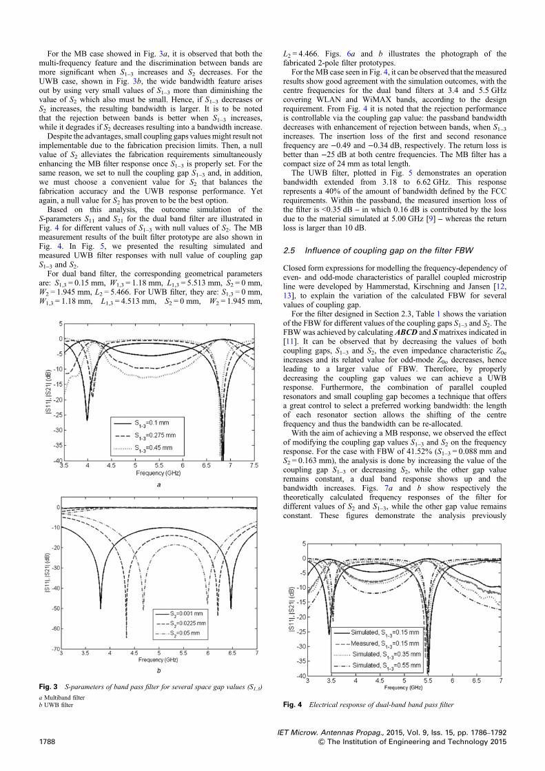
For the MB case showed in Fig. 3a, it is observed that both themulti-frequency feature and the discrimination between bands aremore significant when S1–3 increases and S2 decreases. For theUWB case, shown in Fig. 3b, the wide bandwidth feature arisesout by using very small values of S1–3 more than diminishing thevalue of S2 which also must be small. Hence, if S1–3 decreases orS2 increases, the resulting bandwidth is larger. It is to be notedthat the rejection between bands is better when S1–3 increases,while it degrades if S2 decreases resulting into a bandwidth increase.
Despite the advantages, small coupling gaps valuesmight result notimplementable due to the fabrication precision limits. Then, a nullvalue of S2 alleviates the fabrication requirements simultaneouslyenhancing the MB filter response once S1–3 is properly set. For thesame reason, we set to null the coupling gap S1–3 and, in addition,we must choose a convenient value for S2 that balances thefabrication accuracy and the UWB response performance. Yetagain, a null value for S2 has proven to be the best option.
Based on this analysis, the outcome simulation of theS-parameters S11 and S21 for the dual band filter are illustrated inFig. 4 for different values of S1–3 with null values of S2. The MBmeasurement results of the built filter prototype are also shown inFig. 4. In Fig. 5, we presented the resulting simulated andmeasured UWB filter responses with null value of coupling gapS1–3 and S2.
For dual band filter, the corresponding geometrical parametersare: S1,3 = 0.15 mm, W1,3 = 1.18 mm, L1,3 = 5.513 mm, S2 = 0 mm,W2 = 1.945 mm, L2 = 5.466. For UWB filter, they are: S1,3 = 0 mm,W1,3 = 1.18 mm, L1,3 = 4.513 mm, S2 = 0 mm, W2 = 1.945 mm,
L2 = 4.466. Figs. 6a and b illustrates the photograph of thefabricated 2-pole filter prototypes.
For theMB case seen in Fig. 4, it can be observed that the measuredresults show good agreement with the simulation outcomes, with thecentre frequencies for the dual band filters at 3.4 and 5.5 GHzcovering WLAN and WiMAX bands, according to the designrequirement. From Fig. 4 it is noted that the rejection performanceis controllable via the coupling gap value: the passband bandwidthdecreases with enhancement of rejection between bands, when S1–3increases. The insertion loss of the first and second resonancefrequency are −0.49 and −0.34 dB, respectively. The return loss isbetter than −25 dB at both centre frequencies. The MB filter has acompact size of 24 mm as total length.
The UWB filter, plotted in Fig. 5 demonstrates an operationbandwidth extended from 3.18 to 6.62 GHz. This responserepresents a 40% of the amount of bandwidth defined by the FCCrequirements. Within the passband, the measured insertion loss ofthe filter is <0.35 dB ‒ in which 0.16 dB is contributed by the lossdue to the material simulated at 5.00 GHz [9] ‒ whereas the returnloss is larger than 10 dB.
2.5 Influence of coupling gap on the filter FBW
Closed form expressions for modelling the frequency-dependency ofeven- and odd-mode characteristics of parallel coupled microstripline were developed by Hammerstad, Kirschning and Jansen [12,13], to explain the variation of the calculated FBW for severalvalues of coupling gap.
For the filter designed in Section 2.3, Table 1 shows the variationof the FBW for different values of the coupling gaps S1–3 and S2. TheFBWwas achieved by calculating ABCD and Smatrixes indicated in[11]. It can be observed that by decreasing the values of bothcoupling gaps, S1–3 and S2, the even impedance characteristic Z0eincreases and its related value for odd-mode Z0o decreases, henceleading to a larger value of FBW. Therefore, by properlydecreasing the coupling gap values we can achieve a UWBresponse. Furthermore, the combination of parallel coupledresonators and small coupling gap becomes a technique that offersa great control to select a preferred working bandwidth: the lengthof each resonator section allows the shifting of the centrefrequency and thus the bandwidth can be re-allocated.
With the aim of achieving a MB response, we observed the effectof modifying the coupling gap values S1–3 and S2 on the frequencyresponse. For the case with FBW of 41.52% (S1–3 = 0.088 mm andS2 = 0.163 mm), the analysis is done by increasing the value of thecoupling gap S1–3 or decreasing S2, while the other gap valueremains constant, a dual band response shows up and thebandwidth increases. Figs. 7a and b show respectively thetheoretically calculated frequency responses of the filter fordifferent values of S2 and S1–3, while the other gap value remainsconstant. These figures demonstrate the analysis previously
Fig. 3 S-parameters of band pass filter for several space gap values (S1,3)
a Multiband filterb UWB filter Fig. 4 Electrical response of dual-band band pass filter
IET Microw. Antennas Propag., 2015, Vol. 9, Iss. 15, pp. 1786–17921788 & The Institution of Engineering and Technology 2015
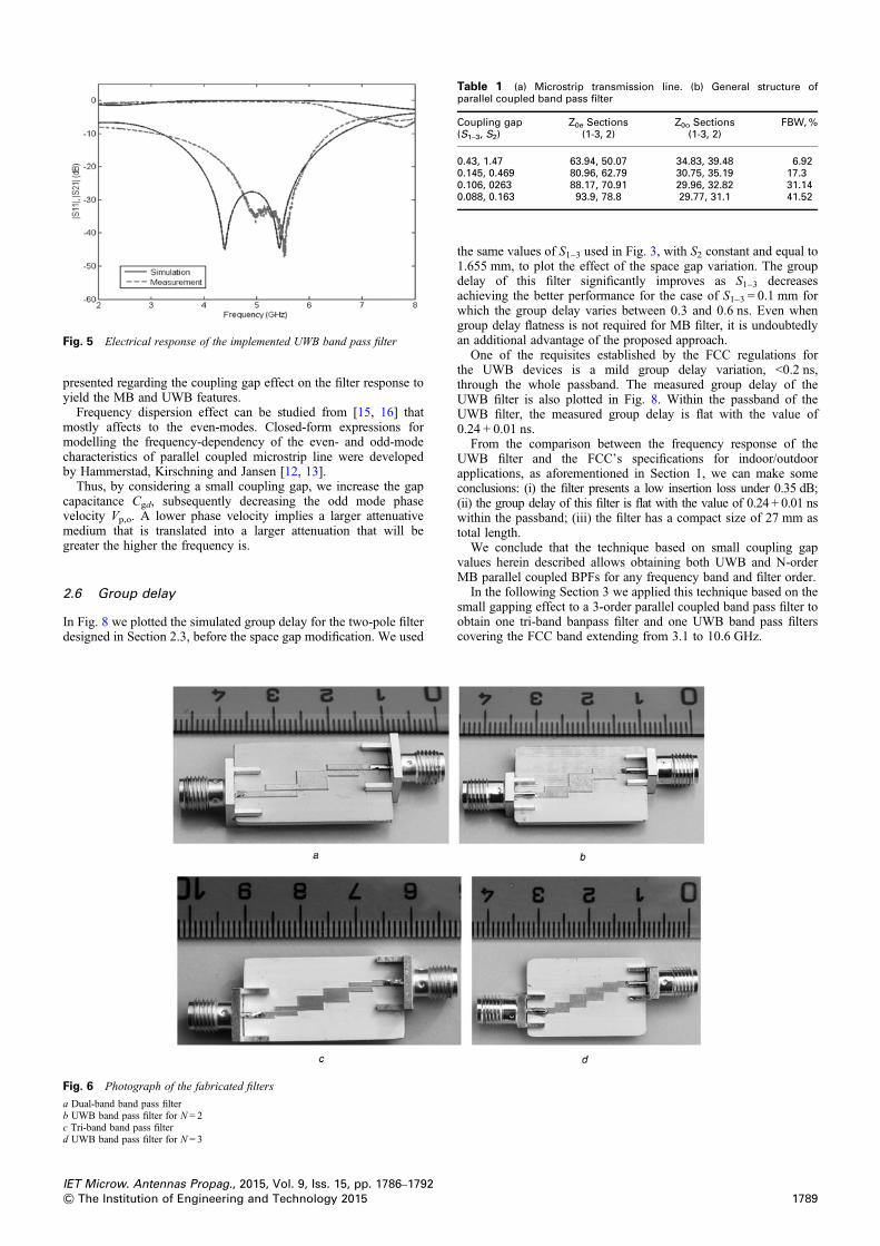
presented regarding the coupling gap effect on the filter response toyield the MB and UWB features.
Frequency dispersion effect can be studied from [15, 16] thatmostly affects to the even-modes. Closed-form expressions formodelling the frequency-dependency of the even- and odd-modecharacteristics of parallel coupled microstrip line were developedby Hammerstad, Kirschning and Jansen [12, 13].
Thus, by considering a small coupling gap, we increase the gapcapacitance Cgd, subsequently decreasing the odd mode phasevelocity Vp,o. A lower phase velocity implies a larger attenuativemedium that is translated into a larger attenuation that will begreater the higher the frequency is.
2.6 Group delay
In Fig. 8 we plotted the simulated group delay for the two-pole filterdesigned in Section 2.3, before the space gap modification. We used
the same values of S1–3 used in Fig. 3, with S2 constant and equal to1.655 mm, to plot the effect of the space gap variation. The groupdelay of this filter significantly improves as S1–3 decreasesachieving the better performance for the case of S1–3 = 0.1 mm forwhich the group delay varies between 0.3 and 0.6 ns. Even whengroup delay flatness is not required for MB filter, it is undoubtedlyan additional advantage of the proposed approach.
One of the requisites established by the FCC regulations forthe UWB devices is a mild group delay variation, <0.2 ns,through the whole passband. The measured group delay of theUWB filter is also plotted in Fig. 8. Within the passband of theUWB filter, the measured group delay is flat with the value of0.24 + 0.01 ns.
From the comparison between the frequency response of theUWB filter and the FCC’s specifications for indoor/outdoorapplications, as aforementioned in Section 1, we can make someconclusions: (i) the filter presents a low insertion loss under 0.35 dB;(ii) the group delay of this filter is flat with the value of 0.24 + 0.01 nswithin the passband; (iii) the filter has a compact size of 27 mm astotal length.
We conclude that the technique based on small coupling gapvalues herein described allows obtaining both UWB and N-orderMB parallel coupled BPFs for any frequency band and filter order.
In the following Section 3 we applied this technique based on thesmall gapping effect to a 3-order parallel coupled band pass filter toobtain one tri-band banpass filter and one UWB band pass filterscovering the FCC band extending from 3.1 to 10.6 GHz.
Fig. 5 Electrical response of the implemented UWB band pass filter
Fig. 6 Photograph of the fabricated filters
a Dual-band band pass filterb UWB band pass filter for N = 2c Tri-band band pass filterd UWB band pass filter for N = 3
Table 1 (a) Microstrip transmission line. (b) General structure ofparallel coupled band pass filter
Coupling gap(S1–3, S2)
Z0e Sections(1-3, 2)
Z0o Sections(1-3, 2)
FBW,%
0.43, 1.47 63.94, 50.07 34.83, 39.48 6.920.145, 0.469 80.96, 62.79 30.75, 35.19 17.30.106, 0263 88.17, 70.91 29.96, 32.82 31.140.088, 0.163 93.9, 78.8 29.77, 31.1 41.52
IET Microw. Antennas Propag., 2015, Vol. 9, Iss. 15, pp. 1786–17921789& The Institution of Engineering and Technology 2015

3 Three-pole Chebyshev band pass filter design
As a second step to illustrate additional details of the synthesis theoryand the advantage of increasing the filter order, we haveimplemented as initial design a Δ = 10% bandwidth Chebyshev
BPF with centre frequency of 5.78 GHz, with order N = 3 andripple of 0.1. The classical design requires ζ0e = 60.72 Ω, ζ0ο =42.57 Ω for Sections 1 and 4, and ζ0e = 51.609 Ω, ζ0ο = 48.48 Ωfor Sections 2 and 3.
The resulting S-parameters of this initial three poles (N = 3) filterare also presented in Fig. 2. It is observed that the simulationperformance shows a very good agreement with the designspecifications. The centre frequency has been fitted to 5.78 GHzwith a bandwidth of about 10%. The corresponding insertion lossof the optimal results is <1 dB with −41.46 dB of return loss inthe desired frequency of 5.78 GHz. The geometrical parametersvalues of this optimised filter design obtained as indicated inSection 2.2, are: S1,4 = 0.608 mm, W1,4 = 1.375 mm, L1,4 = 4.351mm for Sections 1 and 4; S2,3 = 1.911 mm, W2,3 = 1.684 mm, L2,3= 4.306 mm for Sections 2 and 3.
Similarly to the technique described in Section 2.2, we studied theeffect of spacing between each symmetrical section to obtain MBand UWB responses. The performances of the measured andsimulated electrical responses of the resulting tri-band and UWBfilters are shown in Figs. 9 and 10, respectively. Fig. 9 shows thetri-band response for several values of S14, taking S23 as nullgaping. A relative good agreement between measurement andsimulations for the fabricated case, even that some deviations arepresent due to the fabrication tolerances, unideal experimentalconditions (not precise simulation of the connectors, cables,adapters…), and dispersion of the substrate characteristics withrespect to the manufacturer’s datasheet. Furthermore, the rejectionbetween bands and the impedance bandwidth of selectedfrequency pass bands result controllable by the S1–3 value.
According to the measured case outcomes shown in Fig. 9, threenarrow bands were formed with resonant frequencies centred at 3.2,5.78 GHz and 8 GHz covering WiMAX, WLANs and ITU Xfrequency band (from 7.0 to 11.2 GHz). The correspondinginsertion loss and return loss for the tri-band band pass filter wererespectively (−0.82, −20 dB) at 3.2 GHz, (−0.17, −49.16 dB) at5.78 GHz and (−0.17, −42.53 dB) at 8 GHz. It is observed anenhancement of the rejection band in the tri-band response, whenS1–4 increases, similarly to the dual-band analysis presented inSection 2.3.
From Fig. 10, it is apparent that the fabricated filter covers theentire UWB band defined by FCC (3.1–10.6 GHz) and goesbeyond 10.6 GHz, with an insertion loss less than −1 dB withinthe passband and an even better return less than −40 dB. Themeasured group delay of the UWB filter with order N = 3 is alsoplotted in Fig. 8. Within the passband of the UWB filter, themeasured group delay is flat with the value of 0.23 + 0.005 ns.
The physical dimension values of this three-pole Chebyshevparallel coupled band pass filter are: S1,4 = 0.15 mm, W1,4 = 0.98mm, L1,4 = 4.151 mm, S2,3 = 0 mm, W2,3 = 1.31 mm, L2,3 = 4.605mm for the tri-band filter; and S1,4 = 0 mm, W1,4 = 0.98 mm, L1,4 =2.85 mm, S2,3 = 0 mm, W2,3 = 1.31 mm, L2,3 = 3.34 for the UWB
Fig. 7 Calculated filter frequency response for
a Different values of S1,3 and with S2 = 0.088 mmb Different values of S2 and with S1–3 = 0.088 mm
Fig. 9 Electrical response of tri-band band pass filter
Fig. 8 Calculated group delay: for different values of S1–3 of the multiband(MB)l two-pole BPF (Section 2.3), for two-pole UWB filter (Section 2.4) andfor three-pole UWB filter (Section 3)
IET Microw. Antennas Propag., 2015, Vol. 9, Iss. 15, pp. 1786–17921790 & The Institution of Engineering and Technology 2015
case. Figs. 7c and d illustrates a photograph of fabricated filters. TheMB filter has a compact size of 27 mm as total length, and 24 mm forthe UWB case.
We concluded that by setting very small coupling betweenadjacent resonators in the geometry of parallel coupled band passfilter, we can easily approach the desired multi-frequency andUWB responses. By comparison with the few references to asimilar technique found in literature [17, 18], the present synthesistheory incorporates several advantages, such as obtaining MB andUWB band pass filters providing large FBW, low insertion losswithin the passband, delay group flatness, and compact aperturesize without complicating the filter structure. In addition, thepresent technique can be generally used to obtain the MB andUWB performance for any specified frequency band, filter orderand using any dielectric substrate. However, we should indicatethat increasing the filter order does not provide better responsefeatures and it would only increase the filter size withcomplication in controlling the desired frequency pass bands, dueto the presence of an important number of sections thatconsequently yields enlarging the value of critical coupling gaps.It would also require a significant precision in the manufacturingprocess, even more in the MB cases to accurately control thedesired centre frequency and impedance bandwidth.
4 Comparison with other band pass filter designtechniques
Many references found in literature describe works done related toMB and UWB filter design theory. However, among them we cancheck the limited use of the gap reduction technique. Therefore, itis not only possible to make a valid comparison if we considerworks done following different synthesis approaches. For suchcomparison, we decided to consider only techniques based onparallel coupled microstrip designs. Following we divided thecomparison between classical techniques, and other approaches.
First, we compared our synthesis approach proposed in this paperwith classical techniques. Hence, we started focusing on referencesthat work with Chebyshev filter responses, coupled resonators, andmodification of the coupling gap.
In [9] it is shown a sixth order UWB filter based on parallelcoupled microstrip Chebyshev filter that results into a large filterlength and a complicated structure subject to realisticmanufacturing limits. In [14] it is described a UWB design basedon increasing some of those critical filter dimensions to overcomethe fabrication challenges. Filters of order up to nine with FBW of30% or 40% are described in [18].
Different methods and structures based on multiple-moderesonators (MMRs) have been used to develop new UWBband-pass filters which have compact size, low insertion loss,
good selectivity and out-of-band rejection performance [19–24]. In[19], an initial MMR with stepped-impedance configuration wasoriginally reported where the first three resonant modes of theMMR were utilised to design the filter. To achieve good filteringperformance, stepped-impedance-stub loaded resonator was used,and the designed five-mode UWB filter had good filteringperformance and sharp selectivity, but suffered from narrow upperstop-band [20]. To improve the upper stop-band performance, anelectromagnetic band gap embedded MMR [21] andharmonic-suppressed MMR, such as stub-loaded resonators [22]were applied to the design of UWB filters. The size and verticaldimension of the UWB BPF can be significantly reduced byreplacing the modified conventional one quarter-wavelengthparallel coupled lines with cross-shaped coupled lines [23] andalso by the use of radial stub loaded resonator [24], respectively.
Recently, various approaches to implement UWB filtersemploying distributed quarter-wave short-circuited stubs have beendesigned and analysed [25–27]. In [25], compact filters wereobtained by folding the connecting lines and using short-circuitedstubs, however the frequency selectivity achieved by thesestructures was not optimal. In [26], short-circuited stubs werereplaced by open-circuited stubs to accomplish high selectivity,though the size was increased. In [8, 27], the source-load couplingtechnique was used to obtain transmission zeros for a highselectivity and compact size. This technique has been also appliedto other filter types [28, 29]. This set of UWB techniques typicallyachieves over 100% of FBW with an excessive complexity of thefilter structure and enlarging the filter size.
For microwave wireless communication systems, MB filter designhas been an attractive issue, and hence different dual-band andtri-band filter techniques have been developed. In planar circuitry,four basic approaches have been considered to add-inmulti-frequency feature in a filter response. Firstly, by switchingbetween two separate filters at two different frequencies [30]; thisapproach increases size and cost. Secondly, by employing stubs tointroduce transmission zeros which separate pass bands [31]; asthis is essentially a stop band approach, far-out-of-band rejection isimpossible to attain. Thirdly, by using stepped impedanceresonators, that is [32]; however, it is often difficult to achieveproper coupling coefficients for a simultaneous, yet independentcontrol of both in-between frequencies and full bandwidth. Thefourth approach consists of coupled resonator pairs [33], howeverit lacks an independent option to allocate the transmission zeros.
Generally speaking, we conclude that our approach offers anoptimised MB and UWB BPF synthesis design with goodperformance in terms of insertion and return losses, gapcontrollable rejection performance, short dimensions, low orderrequirement, and flat group delay response.
5 Conclusions
This paper proposes a simple filter synthesis technique valid todesign MB and UWB BPF based on parallel coupled microstriplines. This technique consists of modifying the geometry of aninitial classical Chebyshev filter by setting a very small or nullcoupling gap between adjacent resonators so that a MB or anUWB responses are obtained. As an example to validate theproposed synthesis approach, this technique has been applied ontwo and three order initial Chebyshev filters centred at 5.78 GHzdesigned and optimised according to [10, 11]. A posteriori, thecoupling gap between resonators was varied to reach the final MBand UWB approaches. We introduced in Section 2.5 a theoreticalanalysis based on the closed forms given in [12, 13] todemonstrate and explain the effect of the coupling gap variationon the multiband and UWB response from the initial design. Wealso discussed, for the MB design, how the rejection performanceis controllable via the coupling gap value.
In general, the simulation and measurement results of the filtersproposed as example indicate good agreement in term ofS-parameters, insertion and return losses, and group delay, hencevalidating the technique developed in Section 2. The synthesis
Fig. 10 Electrical response of UWB band pass filter
IET Microw. Antennas Propag., 2015, Vol. 9, Iss. 15, pp. 1786–17921791& The Institution of Engineering and Technology 2015

approach described in this work results in a simple structure veryeasy to manufacture with a compact size due to the shorterdimensions and low filter order required, as well as of low-costdue to the implementation in two-layer PCB technology.
We conclude that the excellent results meet the objective of thispaper. A good overall performance is demonstrated for theproposed BPFs in terms of insertion and return losses within thepassbands, as well as FBW and delay group flatness, evencomparing with the requirements established by the FCCregulations. The characteristics of the resulting filters cannot beextensively compared with those found in literature due to thelimited use of the gap reduction technique.
We should note that this technique could be applied as acomplementary step for any design specification, taking as baseany parallel coupled BPF design. Finally, as main disadvantage wecan mention that the UWB filter does not show good steep skirtselectivity and stopband. The attenuation slopes of the skirtsselectivity are not present in this design. The attenuation slopes ofthe skirts selectivity could be improved by insertion of additionalpoles in the lower and upper stopbands.
6 Acknowledgments
This work was funded by the Government of Xunta de Galicia,Spain, (grant no. EMR2012/238), the GreenIT Erasmus MundusProgramme (grant no. 2012-2625/001-001-EMA2), by AtlantiTICResearch Center, and the Spanish Government and the EuropeanRegional Development Fund (ERDF) under project TACTICA.
7 References
1 Federal Communications Commission: ‘Revision of part 15 of the commission’srules regarding ultra-wideband transmission systems’. Technical Report,ET-Docket 98–153, FCC02–48, April 2002
2 Horii, Y.: ‘Design of compact planar ultra-wideband bandpass filters’, inZhurbenko, V. (Ed.): ‘Design of compact planar ultra-wideband bandpass filters,passive microwave components and antennas’ (Intech Open, 2010), pp. 323–339
3 Li, K.: ‘UWB bandpass filter: structure, performance and application to UWB pulsegeneration’. Asia-Pacific Microwave Conf. Proc., Suzhou, China, December 2005,vol. 1
4 Pozar, D.M.: ‘Microwave engineering’ (Wiley and Sons, 2012, 4th edn.)5 Fusco, V.F.: ‘Microwave circuits: analysis and computer-adied design’
(Prentice-Hall International, 1987)6 Zhang, Z.-X., Xiao, F.: ‘An UWB bandpass filter based on a novel type of
multi-mode resonator’, IEEE Microw. Wireless Compon. Lett., 2012, 22, (10),pp. 506–508
7 He, Y., Dong, Y.L.: ‘A novel compact UWB bandpass filter with quarter-waveshort-circuited stubs’. Intelligent Signal Processing and Communication Systems,Chengdu, China, December, 2010, pp. 1–4
8 Shaman, H., Hong, J.S.: ‘A novel ultra-wideband (UWB) bandpass filter (BPF)with pairs of transmission zeroes’, IEEE Microw. Wireless Compon. Lett., 2007,17, (2), pp. 121–123
9 Cai, P., Ma, Z., Guan, X., et al.: ‘Synthesis and realization of novel ultra-widebandbandpass filters using 3/4 wavelength parallel-coupled line resonators’.Asia-Pacific Microwave Conf., Yokohama, Japan, December 2006, pp. 1–4
10 Naghar, A., Aghzout, O., Medina, F., et al.: ‘Study and design of a compact parallelcoupled microstrip band-pass filter for a 5 GHz unlicensed Mobile Wimaxnetworks’, Int. J. Sci. Technol., 2013, 2, (6), pp. 492–497
11 Naghar, A., Aghzout, O., Alejos, A., et al.: ‘Development of a calculator for edgeand parallel coupled microstrip band pass filters’. IEEE Int. Symp. on Antennas andPropagation APS-URSI, Memphis, USA, July 2014
12 Hammerstad, E., Jensen, O.: ‘Accurate models for microstrip computer-aideddesign’. IEEE MTT-S Int. Microwave Symp. Digest, June 1980, pp. 407–409
13 Kirschning, M., Jansen, R.H.: ‘Accurate wide-range design equations for thefrequency dependent characteristic of parallel coupled microstrip lines’, IEEETrans. Microwave Theory Tech., 1984, MTT-32, (1), pp. 83–90
14 Zhu, L., Sun, S., Menzel, W.: ‘Ultra-wideband (UWB) bandpass filters usingmultiple-mode resonator’, IEEE Microwave Wireless Compon. Lett., 2005, 15,(11), pp. 796–798
15 Akhtarzard, S., Rowbotham, T.R., Johns, P.B.: ‘The design of coupled microstriplines’, IEEE Trans. Microw. Theory Tech., 1975, MTT-23, (6), pp. 486–492
16 Sheleg, B., Spielman, B.E.: ‘Characteristics of coupled microstriplines’, IEEE.Trans. Microwave Theory Tech., 2005, 32, (7), pp. 83–89
17 Chin, K.-S., Chiou, Y.-C., Kuo, J.-T.: ‘New synthesis of parallel-coupled linebandpass filters with Chebyshev responses’, IEEE. Trans. Microwave TheoryTech., 2008, 56, (7), pp. 1516–1523
18 Lauer, O., Barras, D., Zahner, M., et al.: ‘Front-end linearity and filter requirementsfor interference robust UWB systems’. Asia-Pacific Int. Symp. on ElectromagneticCompatibility, Beijing, China, April 2010
19 Hao, Z.C., Hong, J.S.: ‘Ultrawideband filter technologies’, IEEE Microw. Mag.,2010, 11, (4), pp. 56–68
20 Chu, Q.X., Wu, X.H., Tian, X.K.: ‘Novel UWB band- pass filters usingstub-loaded multiple-mode resonator’, IEEE Microw. Wirel. Compon. Lett.,2011, 21, (8), pp. 403–405
21 Wong, S.W., Zhu, L.: ‘EBG-embedded multiple-mode resonator for UWBbandpass filter with improved upper-stopband performance’, IEEE Microw.Wirel. Compon. Lett., 2007, 17, (6), pp. 421–423
22 Chu, Q.X., Wu, X.H., Tian, X.K., et al.: ‘Quintuple- mode UWB bandpass filterwith sharp roll-off and super-wide upper stopband’, IEEE Microw. Wirel.Compon. Lett., 2011, 21, (12), pp. 661–663
23 Tian, X.K., Chu, Q.X., Zhu, H., et al.: ‘A UWB bandpass filter with wide stopbandperformance using cross- shaped coupled lines’. Microwave and Millimeter WaveTechnology Int. Conf., Shenzhen, China, 2012, vol. 15, pp. 1–4
24 Xu, J., Wu, W., Kang, W., et al.: ‘Compact UWB bandpass filter with a notchedband using radial stub loaded resonator’, IEEE Microw. Wirel. Compon. Lett.,2012, 22, (7), pp. 351–353
25 He, Y., Dong, Y.L.: ‘A novel compact UWB bandpass filter with quarter-waveshort-circuited stubs’. Intelligent Signal Processing and Communication Systems,Chengdu, China, 2010, pp. 1–4
26 Cai, P., Ma, Z., Guan, X., et al.: ‘A compact UWB bandpass filter using two sectionopen circuited stubs to realize transmission zeros’. Asia-Pacific Microwave Conf.,Suzhou, China, 2005, pp. 4–7
27 Shaman, H., Hong, J.S.: ‘Input and output cross-coupled wideband bandpass filter’,IEEE Trans. Microw. Theory Tech., 2007, 55, (12), pp. 2562–2568
28 Dai, G.L., Guo, Y.X., Xia, M.Y.: ‘Design of compact bandpass filter with improvedselectivity using source-load coupling’, IET Electron. Lett., 2010, 46, (7),pp. 505–506
29 Wang, H., Chu, Q.X.: ‘A narrow-band hairpin-comb two-pole filter withsource-load coupling’, IEEE Microw. Wireless Compon. Lett., 2010, 20, (7),pp. 372–374
30 Miyake, H., Kitazawa, S., Ishizaki, T., et al.: ‘A miniaturized monolithic dual-bandfilter using ceramic lamination technique for dual-mode portable telephones’. IEEEMTT-S Int. Microwave Symp. Digest, 1997, pp. 789–792
31 Quendo, C., Ruis, E., Person, C.: ‘An original topology of dual band filter withtransmission zeros’. IEEE MTT-S Int. Microwave Symp. Digest, 2003,pp. 1093–1096
32 Chang, S.F., Jeng, Y.H., Chen, J.L.: ‘Dual-band step-impedance bandpass filter formultimode wireless LANs’, IET Electron. Lett., 2004, 40, (1), pp. 38–39
33 Chen, C.C.: ‘Dual-band bandpass filter using coupled resonator pairs’, IEEEMicrow. Wirel. Comp. Lett., 2005, 15, (4), pp. 259–261
IET Microw. Antennas Propag., 2015, Vol. 9, Iss. 15, pp. 1786–17921792 & The Institution of Engineering and Technology 2015
Influence of impairments due to dispersive propagation on theantenna design for body-based applications
Ana Vazquez Alejosa* , Muhammad Dawoodb, Erik Aguirrec, Francisco Falconec,David Alvarez Outereloa, Azzedin Naghard and Otman Agzhoutd
aTeoria de la Señal y Comunicaciones, University of Vigo, Vigo, Spain; bKlipsch School ofElectrical and Computer Engineering, New Mexico State University, Las Cruces, NM, USA;
cElectrical and Electronic Engineering Department, Universidad Pública de Navarra, Pamplona,Spain; dFaculty of Science, Abdelmalek Essaadi University, Tetouan, Morocco
(Received 29 April 2015; accepted 28 September 2015)
In this paper, we analyze the frequency-dependent feature of the human body asradio propagation channel and the influence of that characteristic on the design ofantennas for body-based applications. We describe the main impairments due to thefrequency dispersion propagation through the body channel. Firstly, we describe theformation of the electromagnetic fields called Brillouin precursors which are respon-sible for another vital impairment: broadening of the time width of a transmitted sig-nal. Later, we show a theoretical radio channel characterization of a human tissuethat is affected by the frequency dispersion. Following, we describe three solutionsto the described problematic optimal design of waveforms matched to the bodychannel, anti-dispersive filtering, and optimal antenna design. We introduce twobroadband antennas offering a flat frequency response, minimizing the formation ofprecursors that ensures optimal time domain performance for ultrawideband body-based applications. Finally, we discuss the relation between the precursor formationand the parameters adopted to quantify the electromagnetic absorption inside biolog-ical tissues in order to review its definition under the dispersive perspective.
Keywords: dispersive electromagnetic; Brillouin precursor; radio channel; bodycommunications; antenna; waveform design
1. Introduction
Wireless body area network (WBAN) communications, either on-body or intra-body,have been designed for a specific environment for which it is commonly accepted thatthe frequency dependence of the dielectric properties of the human body tissues canseverely affect the performance of the systems intended to accomplish these communi-cations.[1–5]
The frequency-dependent behavior of the biological media can result in the forma-tion of Sommerfeld and Brillouin precursor fields, an electromagnetic waveform usuallyrelated to the lower frequency components of the propagated signal.[1,6] Oughstun in[1] concludes that the Brillouin precursor is the dominant electromagnetic componentof a signal propagating through most of dispersive materials below resonant frequen-cies. The Brillouin precursor is characterized by an algebraically amplitude decay incontradiction to the Bouger–Lambert–Beer law, whereby each nonzero frequency
*Corresponding author. Email: [email protected]
© 2015 Taylor & Francis
Journal of Electromagnetic Waves and Applications, 2015Vol. 29, No. 17, 2355–2364, http://dx.doi.org/10.1080/09205071.2015.1103667
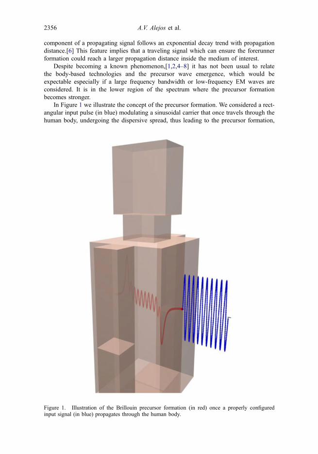
component of a propagating signal follows an exponential decay trend with propagationdistance.[6] This feature implies that a traveling signal which can ensure the forerunnerformation could reach a larger propagation distance inside the medium of interest.
Despite becoming a known phenomenon,[1,2,4–8] it has not been usual to relatethe body-based technologies and the precursor wave emergence, which would beexpectable especially if a large frequency bandwidth or low-frequency EM waves areconsidered. It is in the lower region of the spectrum where the precursor formationbecomes stronger.
In Figure 1 we illustrate the concept of the precursor formation. We considered a rect-angular input pulse (in blue) modulating a sinusoidal carrier that once travels through thehuman body, undergoing the dispersive spread, thus leading to the precursor formation,
Figure 1. Illustration of the Brillouin precursor formation (in red) once a properly configuredinput signal (in blue) propagates through the human body.
2356 A.V. Alejos et al.
which is visible as superimposed fields in the leading and trailing edges of the red wave-form.
The dispersive propagation undergone by the signal traveling through a mediumsuch as the body channel can strongly condition the received signal due to the produc-tion of undesired effects, the main of which is the broadening of the time durationundergone by the signal propagating through the dispersive media, so turning the fre-quency dispersion into an extremely important impairment is to be considered in thedesign of receiver systems,[4,9] or in order to ensure the reliability of the propagationthrough this kind of media, as in the case of intra-body communications. E.g., for thecase of a sequence of pulses, at a given propagation distance, the broadening experi-enced by a traveling pulse in its time width can lead to a destructive merge of theinformation which would make impossible and totally erroneous the informationretrieval.[9]
This phenomenon depends on the dielectric properties of the underlying medium aswell as on other parameters or settings, e.g. the input signal type and its configuration,as well as the involved transmitted and/or received bandwidth.[1,9]
In Section 2, we describe the main impairments due to the precursor formation andtheir effects on the body-based applications, mainly from the point of view of intra-body radio propagation. We have also considered solutions to such problems. In Sec-tion 2.4, we introduce the time domain analysis of two frequency-flat response antennasdesigned to diminish the formation of precursor fields, as well as to avoid distortingthe transmitted pulses. In Section 3, we discuss the power extinction decay trend forintra-body radio channel and its relation to the specific absorption rate (SAR). Finally,conclusions are offered in Section 4.
2. Formulation of dispersive propagation
Here, we reflect on the most important aspects and impairments related to the fre-quency dispersion and the precursor formation, as well as we describe three approachesvalid to solve the created problematic.
2.1. Radio channel characterization for a dispersive medium
The frequency dispersive nature of the body channel alters the propagation of widebandor low-frequency signals and therefore can distort the radio channel characterization ofintra-body radio propagation: the broadening and amplitude level distortion undergoneby the transmitted pulses will introduce uncertainty or noise, leading to a larger degra-dation of the cross-correlation function (CCF), and consequently masking the returnechoes detection.[5]
This fact especially affects broadband communications, for which multipath interfer-ence can be difficult to characterize and control. Different solutions are described asfollows:
2.2. Optimal transmitting waveform design
The evolution of an input signal x(t) was evaluated in the frequency domain in off-linemode, just considering the frequency response of the dispersive medium H(z, f), andthe propagation distance travelled z inside the medium. Then, it is enough to multiplyY(f) = X(f)∙H(f), where X(f) is the input signal in the spectrum domain, and then apply
Journal of Electromagnetic Waves and Applications 2357

an inverse fast Fourier transform to observe the output signal in the time domain, y(t).The estimation of the frequency response H(z, f) of the dispersive medium agrees witha general transmission coefficient definition as described in (1) [4,9]:
Hðz; f Þ ¼ ejcmðf Þz (1)
with γm(f) the medium propagation constant derived as in (2):
cm xð Þ ¼ a xð Þ þ j b xð Þ ¼ xc
ffiffiffiffiffiffiffiffiffiffiffier xð Þ
p(2)
The outcome H(z, f) contains information about the effects of attenuation and phase foreach frequency component of the signal traveling through the medium under study.The result is then a frequency filter H(z, f) and is valid for analysis of precursor evolu-tion for any input signal x(z, t) propagating through the dispersive medium character-ized by H(z, f ) for any penetration depth z. The model representing the complexdielectric properties of the underlying dispersive media is of vital importance since it isused to estimate the propagation constant γm(f ) in (2). The dielectric properties willfingerprint indeed the resulting Brillouin precursor.
In Figure 2, we show the theoretical evolution of a rectangular pulse provided with asine carrier of center frequency f0 = 6 GHz and time duration Tb = 10/f0 through a singlelayer of tissue N1 characterized by a Cole–Cole model.[10] We observe the largewaveform shape distortion, as well as the early extinction of the carrier component(cycles within edges). This result is particularly important for intra-body communica-tions. It implies that a wideband transmission will be severely affected by the dispersive
0 1 2 3 4 5 6 7 8 9 10-1
-0.8
-0.6
-0.4
-0.2
0
0.2
0.4
0.6
0.8
1
time (t/Tb)
rela
tive
ampl
itude
(V)
Input signalRect, Tissue N1, Cole-Cole, Tb=10/f0, z=1zdRect, Tissue N1, Cole-Cole, Tb=10/f0, z=5zdRect, Tissue N1, Cole-Cole, Tb=10/f0, z=9zd
Figure 2. Theoretical evolution of a rectangular pulse after propagating through different dis-tances within a layer of tissue N1: at input (z = 0), z = 1∙zd, z = 5∙zd and z = 9∙zd, with zd = e-α,and α the propagation constant of the tissue in Np.
2358 A.V. Alejos et al.
propagation and robust input signals and proper spectrum frequency windows must bechosen.[9]
For intra-body communications, the form and shape of the information-bearingtransmitted signal is an important factor to consider.[11,12] Since the transmitted signalinfluences the formation and performance of the resulting precursor, we can concludethat a medium-matched signal can lead to optimal performance by combining the bene-fits of the precursor formation (larger amplitude) with minor impairments (lesser timeduration broadening).[12]
2.3. Anti-dispersive filtering
As in radar technology, an anti-dispersive (AD) filtering can be implemented on thereceiver end to compensate the frequency dispersive effects.[11] However, this solutionrequires the a priori knowledge of the propagation scenario, also in terms of multipathcharacteristics. On the transmitter end, an AD element [13] could be also considered asan element prior to the antenna or well embedded on it, in order to match the signal toa specific medium and propagation scenario, so as to achieve a signal propagation infrequency flat mode; however, this solution is also a pulse shaping technique that doesnot prevent the need to use an AD filtering on the receiver end.
However, it should be noted that AD elements are very sensitive to design errorsand variations of the medium dielectric properties. Solutions presented in [11] alsoaccount for the variation in the tissues response with the distance propagated by thesignal within them.[13]
2.4. Antenna design
The antenna can be also used as an AD element, or simply can be designed to show aflat frequency response, in order to avoid worsening the impairments due to the fre-quency-dependent body channel. Following, we describe two antennas designed andbuilt with flat-frequency response and improved time domain performance (Figure 3).
The first antenna model selected to be implemented was a UWB ridged horn. Mate-rial selected was a blend of copper and brass (40%, 60%), and in the waveguide-to-coaxial adaptor, it was used an N male connector. The UWB horn antenna dimensionsare (in mm): Ha = 46.67, Wa = 66.67, Lf = 53.33, Hg = 9.467, Wg = 14.95, Lg = 5.2,Wr = 4.88, Sr = 666.7, Lsr = 3.333, Hsr = 473.3, Wc = 0.976, Sf = 1.017, θc = 45°,Di = 0.4167, Do = 1.367. The relative dielectric permittivity of the coaxial feeder wasεr = 2.05.
The UWB horn can operate in the range 3–11 GHz, with a VSWR less than 1.5,and the return loss was under −15 dB. The antenna gain was 9.7 dBi (@7 GHz) with adeviation of 2.7 dBi. The antenna beamwidth was 56.81° (E-plane) and 52.72°(H-plane). Both parameters were obtained from measurements in an anechoic chamber.
For the printed UWB antenna, the geometry parameters were (in mm): L1 = 13.5,L2 = 9.5, L3 = 3, L4 = 26, W1 = 2.8, W2 = 14, W3 = 2.02, W4 = 28, n1 = 0.96, n2 = 0.74,n3 = 0.45, m1 = 3.96, m2 = 3.19, m3 = 3.02. The antenna was printed on low-cost FR-4substrate material with relative dielectric constant of 4.4, loss tangent of 0.02, andthickness of 1.6 mm. The antenna physical dimensions correspond to an electrical sizeof 0.25λ.
The printed UWB antenna can operate through an impedance bandwidth rangingfrom 3.6 to 11 GHz, with a VSWR less than 2, and a measured return loss was under
Journal of Electromagnetic Waves and Applications 2359
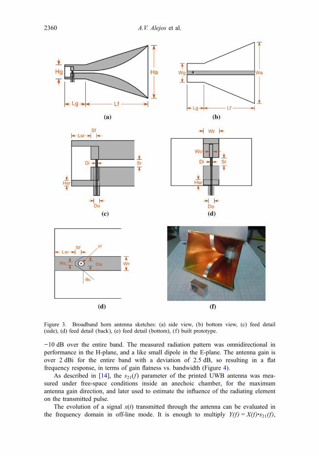
−10 dB over the entire band. The measured radiation pattern was omnidirectional inperformance in the H-plane, and a like small dipole in the E-plane. The antenna gain isover 2 dBi for the entire band with a deviation of 2.5 dB, so resulting in a flatfrequency response, in terms of gain flatness vs. bandwidth (Figure 4).
As described in [14], the s21(f) parameter of the printed UWB antenna was mea-sured under free-space conditions inside an anechoic chamber, for the maximumantenna gain direction, and later used to estimate the influence of the radiating elementon the transmitted pulse.
The evolution of a signal x(t) transmitted through the antenna can be evaluated inthe frequency domain in off-line mode. It is enough to multiply Y(f) = X(f)∙s21(f ),
Figure 3. Broadband horn antenna sketches: (a) side view, (b) bottom view, (c) feed detail(side), (d) feed detail (back), (e) feed detail (bottom), (f) built prototype.
2360 A.V. Alejos et al.

where X(f ) is the input signal in the spectrum domain, and then apply an inverse fastFourier transform to observe the output signal in the time domain, y(t). The pulse gen-eration is then not necessary in the transmitter end, and a digitalization stage is neitherneeded in the receiver. Both generator and digitizer stages could cause important inac-curacies due to the filtering effect introduced and the digitalization error. The input sig-nal x(t) consisted of a baseband pulse modulating a sine carrier at f0 = 7.5 GHz.
In Table 1, we show the value of the correlation factor in percentage estimatedbetween the signal originally fed into the antenna and the signal obtained after trans-mission. Four different baseband pulses commonly found in UWB applications havebeen analyzed for three durations of the pulse time width Tb – inversely related to thepulse bandwidth – measured in terms of 1/f0. The ρ values are given in pairs corre-sponding to the two UWB antennas: horn and printed.
Figure 4. UWB antenna: geometry of the antenna with detail of ground plane and picture of thefabricated prototype with a SMA connector.
Table 1. Variation of correlation factor in percentage.
Pulse ρ (%), Tb = 10/fc ρ (%), Tb = 5/fc ρ (%), Tb = 1/fc
Lorentz 0.5/[1 + (t/Tb)2] 98, 93 73, 80 20, 22
Impulse δ(t − 0.125Tb) <10, <10 <10, <10 <10, <10Exponential exp[−2t/Tb] 66, 74 50, 55 17, 21Rectangular ∏(t/Tb) 80, 81 62, 66 29, 33
Journal of Electromagnetic Waves and Applications 2361

The larger the input pulse bandwidth, the more critical becomes the effect of thefrequency dispersion induced by the antenna on the input pulse mainly due to the emer-gence of the precursor field, and then the correlation factor ρ decreases considerably.With this off-line method, we have shown that the distortion undergone as a result ofthe formation of precursor fields, derived of the frequency dependence of the antennatransfer function observed in the response s21(f), avoided inaccuracies and errors due tothe measurement hardware.
3. Simulation results
Among other distinguished properties, once the precursors are formed, these superim-posed fields achieve an algebraically peak level decay that also implies a lower powerextinction trend within the medium.[8,15] From the dosimetric point of view, that largerpower level requires to review the exposure values under the circumstances of fre-quency dispersive propagation [5,16]:
• The magnitude of the reference parameter adopted for limiting the exposure toelectromagnetic fields, the specific absorption rate (SAR), was defined in thenear-field only between 100 kHz and 10 GHz, and only considers the time varia-tion of sinusoidal signals.
• An effective and correct exposure for spread spectrum or ultrawideband signals isonly achieved if all employed frequencies are used.[5,16,17] The time integral ofSAR is known as specific absorption (SA) and could represent a valid approachto obtain an effective exposure for multi-frequency signals.
• A fully valid approach would be given in the frequency domain, considering thedefinition of SA according to Parserval’s theorem [17]:
SA ¼Z
r xð Þ E xð Þj j2dx (3)
where σ(ω) is the conductivity and E(ω) is the Fourier transfer of the propagated elec-tric field E(t).
4. Conclusions
In this paper, we reflect on the key role that the frequency dispersive nature of thehuman tissues can play in body-based applications. We discussed on the importance ofthe precursor fields related to body-based applications and the further research neededin this direction. Furthermore, we demonstrated that specific pulses and waveforms canbe designed to achieve an optimal propagation within the medium of interest, such asthe case of the Brillouin pulse.
The precursor retains most of the energy of the traveling signal and this energy alsofollows an algebraically decay trend.[8,15] This fact can likely influence the estimationof the SAR.[5] It is clear that considering jointly multi-frequency component signalsand the dispersive propagation phenomenon, the SA value would result more meaning-ful than the SAR single values. The exposure limits would then require a review underthe perspective herein exposed, especially for the frequency band assigned by the FCCfor ultrawideband medical technologies or the lower portion of the spectrum, both ofwhich result inherently dispersive.
2362 A.V. Alejos et al.

We have also shown that the antenna design can control the effects of the frequencydispersion induced by the antenna response and so fading the precursor field formation.
Regarding the novelty of the research here conducted, we would like to notice thatit is the first time that precursor energy characteristics is considered jointly to the SARand SA estimation for wideband signals in order to analyze the impact on plausiblebody-based applications. A detailed discussion of the health and safety issues associ-ated with UWB electromagnetic radiation traveling through human tissues is presentedin [18], only theoretically derived.
Even when the paper presents an ideal analysis based on few assumptions, formerpublished evidences exist for validating this analysis and also practical examples areavailable in the literature.
The theoretically achieved results presented here rely on experimental results for-merly published that demonstrated the benefits of considering the dispersive analysisfor propagation through water,[19] vegetation [20,21], and soil.[22]
Finally, we notice that the practical applicability of the precursor features has beenreflected in a few patents; however, only two of them applied to the microwave region:in [23], it is claimed the use of a radar transmitting a Brillouin-like pulse and in [24], itis described a method to analyze the practical estimation of dispersive propagation forany media.
Further analysis should be conducted, mainly at experimental level, even wheninvolving human biology increases the complexity of the measurement scenarios andimplies a not negligible amount of legal considerations.
Disclosure statement
No potential conflict of interest was reported by the authors.
FundingThis work was supported by the Xunta de Galicia (Spain) [grant number EMR2012/138].
ORCID
Ana Vazquez Alejos http://orcid.org/0000-0003-3426-2909Azzedin Naghar http://orcid.org/0000-0002-3706-2948
References[1] Oughstun KE. Electromagnetic and optical pulse propagation. Vol. 2. ed. Berlin: Springer-
Verlag; 2009.[2] Albanese R, Penn J, Medina R. Short-rise-time microwave pulse propagation through disper-
sive biological media. J. Opt. Soc. Am. A. 1989;6:1441–1446.[3] Scanlon WG, Burns B, Evans NE. Radiowave propagation from a tissue-implanted source at
418 MHz and 916.5 MHz. IEEE Trans. Biomed. Eng. 2000;47:527–534.[4] Alejos AV, Falcone F, Dawood M, et al. Evaluation of the Brillouin precursor performance
for ultra wide band intra-body technologies. J. Electromagn. Waves App. 2013;27:2213–2220.
[5] Alejos AV, Falcone F, Aguirre E, et al. Performance evaluation of medium-matched wave-forms and pulse shaping for application in ultrawideband intra-body technologies. IEEE/URSI International Symposium on Antennas and Propagation; 2013 July; Orlando, FL,USA.
Journal of Electromagnetic Waves and Applications 2363
[6] Cartwright N. Low frequencies and the Brillouin precursor. IEEE Trans. Antennas Propag.2011;59:1571–1579.
[7] Pieraccini M, Bicci A, Mecatti D, et al. Propagation of large bandwidth microwave signalsin water. IEEE Trans. Antennas Propag. 2009;57:3612–3618.
[8] Safian R, Sarris CD, Mojahedi M. On the transmission and propagation of low attenuationrate electromagnetic pulses in debye media. IEEE Trans. Antennas Propag. 2009;57:3676–3680.
[9] Alejos AV, Dawood M, Falcone F. Temporal and frequency evolution of Brillouin andSommerfeld precursors through dispersive media in THz-IR bands. IEEE Trans. AntennasPropag. 2012;60:5900–5913.
[10] Gabriel C. Compilation of the dielectric properties of body tissues at RF and microwave fre-quencies. Brooks Air Force, Brooks AFB, TX, Tech. Rep. AL/OE-TR-1996–0037; 1996.
[11] Santoreli A, Porter E, Popovic M, et al. Pulse shaping for time-domain microwave breasttumour detection: experiments with realistic tissue phantoms. European Conference onAntennas and Propagation, IEEE Trans. Geosci. Remote Sens., Prague (Chec Republic);2012.
[12] Alejos AV, Dawood M, Mohammed HUR. Empirical pseudo-optimal waveform design fordispersive propagation through loamy soil. IEEE Geosci. Remote Sens. Lett. 2012;9:953–957.
[13] Alejos AV. Understanding the design of anti-dispersive filtering for propagation of UWBmicrowave signals in dispersive soils. IEEE Geosci. Remote Sens. Lett. 2014;11:14–18.
[14] Costa JR, Medeiros CR, Fernandes CA. Performance of a crossed exponentially tapered slotantenna for UWB systems. IEEE Trans. Antennas Propag. 2009;57:1345–1352.
[15] Alejos AV, Dawood M. Estimation of power extinction factor in presence of Brillouin pre-cursor formation through dispersive media. J. Electromagn. Waves App. 2011;25:455–465.
[16] Sánchez-Hernández DA. High frequency electromagnetic dosimetry. Boston (MA): ArtechHouse; 2009. Chapter 2.
[17] Wang Q, Wang J. SA/SAR analysis for multiple UWB pulse exposure. In: ElectromagneticCompatibility and 19th International Zurich Symposium on Electromagnetic Compatibility;Singapore; 2008. p. 212–215
[18] Oughstun KE. Electromagnetic and optical pulse propagation. Vol. 2. ed. Berlin: Springer-Verlag; 2009. Chapter 9, Applications; p. 713–776.
[19] Mohammed H, Dawood M, Alejos AV. Experimental detection of Brillouin precursorsthrough tap water at microwave frequencies. IET Electron. Lett. 2010;42:1645–1647.
[20] Alejos AV, Dawood M, Mohammed HUR. Analysis of Brillouin precursor propagationthrough foliage for digital sequences of pulses. IEEE Geosci. Remote Sens. Lett.2011;8:59–63.
[21] Alejos AV, Dawood M, Medina L. Experimental dynamical evolution of the Brillouin pre-cursor for broadband wireless communication through vegetation. Prog. Electromagn. Res.2011;111:291–309.
[22] Mohammed H, Dawood M, Alejos AV. Experimental detection and characterization of Bril-louin precursor through loamy soil at microwave frequencies. IEEE Trans. Geosci. RemoteSens. 2012;50:436–445.
[23] Lockheed Martin Corporation, assignee. Method and apparatus for precursor based radar.United States patent US 6,429,801 B1. 2000 Oct 19.
[24] Dawood M, Mohammed HUR, Alejos AV, inventors; Arrowhead Center, Inc., assignee.Method, technique, and system for detecting Brillouin precursors at microwave frequenciesfor enhanced performance in various applications. United States patent US 8,570,207 B1.2010 Jun 9.
2364 A.V. Alejos et al.
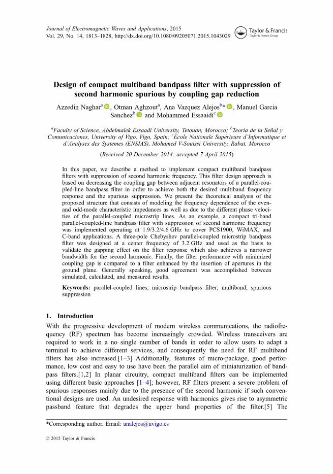
Design of compact multiband bandpass filter with suppression ofsecond harmonic spurious by coupling gap reduction
Azzedin Naghara , Otman Aghzouta, Ana Vazquez Alejosb* , Manuel GarciaSanchezb and Mohammed Essaaidic
aFaculty of Science, Abdelmalek Essaadi University, Tetouan, Morocco; bTeoria de la Señal yComunicaciones, University of Vigo, Vigo, Spain; cEcole Nationale Supérieure d’Informatique et
d’Analyses des Systemes (ENSIAS), Mohamed V-Souissi University, Rabat, Morocco
(Received 20 December 2014; accepted 7 April 2015)
In this paper, we describe a method to implement compact multiband bandpassfilters with suppression of second harmonic frequency. This filter design approach isbased on decreasing the coupling gap between adjacent resonators of a parallel-cou-pled-line bandpass filter in order to achieve both the desired multiband frequencyresponse and the spurious suppression. We present the theoretical analysis of theproposed structure that consists of modeling the frequency dependence of the even-and odd-mode characteristic impedances as well as due to the different phase veloci-ties of the parallel-coupled microstrip lines. As an example, a compact tri-bandparallel-coupled-line bandpass filter with suppression of second harmonic frequencywas implemented operating at 1.9/3.2/4.6 GHz to cover PCS1900, WiMAX, andC-band applications. A three-pole Chebyshev parallel-coupled microstrip bandpassfilter was designed at a center frequency of 3.2 GHz and used as the basis tovalidate the gapping effect on the filter response which also achieves a narrowerbandwidth for the second harmonic. Finally, the filter performance with minimizedcoupling gap is compared to a filter enhanced by the insertion of apertures in theground plane. Generally speaking, good agreement was accomplished betweensimulated, calculated, and measured results.
Keywords: parallel-coupled lines; microstrip bandpass filter; multiband; spurioussuppression
1. Introduction
With the progressive development of modern wireless communications, the radiofre-quency (RF) spectrum has become increasingly crowded. Wireless transceivers arerequired to work in a no single number of bands in order to allow users to adapt aterminal to achieve different services, and consequently the need for RF multibandfilters has also increased.[1–3] Additionally, features of micro-package, good perfor-mance, low cost and easy to use have been the parallel aim of miniaturization of band-pass filters.[1,2] In planar circuitry, compact multiband filters can be implementedusing different basic approaches [1–4]; however, RF filters present a severe problem ofspurious responses mainly due to the presence of the second harmonic if such conven-tional designs are used. An undesired response with harmonics gives rise to asymmetricpassband feature that degrades the upper band properties of the filter.[5] The
*Corresponding author. Email: [email protected]
© 2015 Taylor & Francis
Journal of Electromagnetic Waves and Applications, 2015Vol. 29, No. 14, 1813–1828, http://dx.doi.org/10.1080/09205071.2015.1043029

phenomenon of second harmonic spurious response is due to the unequal phasevelocities of the even and odd modes, creating different multiples of the half wave-length λ0/2 corresponding to the fundamental frequency, for both modes. In a homoge-neous transmission line such as a strip line, these half wavelength frequencies arecoincident, therefore creating a zero in the filter response at these harmonic frequenciesvalues. However, the inhomogeneous nature of microstrip does not allow the halfwavelength frequencies to coincide, consequently leading to a nonzero response atmultiple or harmonics of the fundamental frequency considered for the filter design(2f0, 4f0, and so on).
Recently, diverse techniques have been reported and the set of approaches share theidea of modifying the structure of the microstrip filter by some means, among whichwe can mention the use of dielectric overlay, ground apertures insertion, by consideringPBG structures, substrate suppression, periodic grooves design, or use of wiggly linetechniques and filters using fractal shapes.[6–8] In this paper, an approach valid todesign multiband parallel-coupled bandpass filter with spurious response suppression at2f0, without changing the basic geometry of the filter structure is proposed. Theapproach consists of creating small coupling gap between the coupled parallel sectionsas a method to accomplish both a multiband response as well as the second harmonicreduction. Jointly to this solution, we introduced apertures in the ground plane [6] andgrooves in the substrate [8] in order to compare both techniques – coupling gap reduc-tion and ground apertures – in terms of suppression of the second harmonic present inthe bandpass filter response.
The theoretical analysis of the solution based on small coupling gap and its effect onthe filter response was detailed in Section 2. In Section 3, as an application example ofthe proposed filter design technique, we implemented a multiband filter operating at thecenter frequencies of 1.9, 3.2, and 4.6 GHz used for PCS1900 (Personal communica-tions service), WiMAX (Worldwide interoperability Microwave Access), and super-extended C-band systems, respectively. The design procedure consisted of three steps:from a basic bandpass filter structure to an optimal multiband response design with sup-pression of second harmonic spurious by sequentially integrating the above-indicatedtwo techniques. To this aim, initially a conventional parallel-coupled bandpass filter at3.2 GHz was designed, as described in Section 3.1; then, by implementing a small andnull spacing between resonators – coupling gap – we obtained a tri-band filter responsewith spurious minimization, as indicated in Section 3.2. Finally, the achieved secondharmonic suppression was compared to the enhancement due to the addition of groundplane apertures and substrate grooves, as shown in Section 3.3. In Section 3.4, we dis-cuss the effect of the resonator length on the center resonant frequencies and then on thefilter response. The proposed filter was simulated and optimized using the commercialelectromagnetic simulator CST MW. To validate the performance of the design proce-dure, a comparison between theoretical and measurement results is presented, showinggood agreement and proving that the size, performance, and characteristics of theaccomplished multiband filter have been optimized.
2. Theoretical analysis of multiband filter design
As aforementioned, the approach valid to design parallel-coupled bandpass filter withmultiband response and spurious response suppression at 2f0, consists of two combinedtechniques: (1) making small coupling gap between the coupled parallel sections toaccomplish the aimed multiband response and minimize the spurious due to the second
1814 A. Naghar et al.
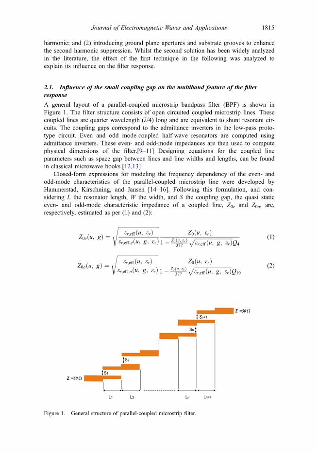
harmonic; and (2) introducing ground plane apertures and substrate grooves to enhancethe second harmonic suppression. Whilst the second solution has been widely analyzedin the literature, the effect of the first technique in the following was analyzed toexplain its influence on the filter response.
2.1. Influence of the small coupling gap on the multiband feature of the filterresponse
A general layout of a parallel-coupled microstrip bandpass filter (BPF) is shown inFigure 1. The filter structure consists of open circuited coupled microstrip lines. Thesecoupled lines are quarter wavelength (λ/4) long and are equivalent to shunt resonant cir-cuits. The coupling gaps correspond to the admittance inverters in the low-pass proto-type circuit. Even and odd mode-coupled half-wave resonators are computed usingadmittance inverters. These even- and odd-mode impedances are then used to computephysical dimensions of the filter.[9–11] Designing equations for the coupled lineparameters such as space gap between lines and line widths and lengths, can be foundin classical microwave books.[12,13]
Closed-form expressions for modeling the frequency dependency of the even- andodd-mode characteristics of the parallel-coupled microstrip line were developed byHammerstad, Kirschning, and Jansen [14–16]. Following this formulation, and con-sidering L the resonator length, W the width, and S the coupling gap, the quasi staticeven- and odd-mode characteristic impedance of a coupled line, Z0e and Z0o, are,respectively, estimated as per (1) and (2):
Z0eðu; gÞ ¼ffiffiffiffiffiffiffiffiffiffiffiffiffiffiffiffiffiffiffiffiffiffiffiffiffiffiffiffiffiffiffier;eff ðu; erÞ
er;eff ;eðu; g; erÞ
sZ0ðu; erÞ
1 Z0ðu; erÞ377
ffiffiffiffiffiffiffiffiffiffiffiffiffiffiffiffiffiffiffiffiffiffiffiffiffiffiffiffier;eff ðu; g; erÞ
pQ4
(1)
Z0oðu; gÞ ¼ffiffiffiffiffiffiffiffiffiffiffiffiffiffiffiffiffiffiffiffiffiffiffiffiffiffiffiffiffiffiffier;eff ðu; erÞ
er;eff ;oðu; g; erÞ
sZ0ðu; erÞ
1 Z0ðu; erÞ377
ffiffiffiffiffiffiffiffiffiffiffiffiffiffiffiffiffiffiffiffiffiffiffiffiffiffiffiffier;eff ðu; g; erÞ
pQ10
(2)
Figure 1. General structure of parallel-coupled microstrip filter.
Journal of Electromagnetic Waves and Applications 1815
with Z0(u, g) the static characteristic impedance of a single microstrip line of width W,and εr,eff,e(u, g, εr) and εr,eff,o(u, g, εr) the effective relative dielectric permittivity of theeven and odd modes that are obtained by (3) and (4):
er;eff ;eðu; g; erÞ ¼ 0:5ðer þ 1Þ þ 0:5ðer 1Þ 1þ 10=vð ÞaeðvÞbeðerÞ (3)
er;eff ;oðu; g; erÞ ¼ ½0:5ðer þ 1Þ þ a0ðu; erÞ er;eff ð0Þ expðc0gd0Þ þ er;eff ð0Þ (4)
with the pair (u = W/h, g = S/h) as the normalized strip width and line spacing for asingle microstrip line; ae, be, c0, and d0 the parameters related to the even and oddmodes; and εr,eff(0) the effective dielectric constant of a single microstrip of null widthW. More details of the background formulas required to infer (1)–(4) can be found in[14–16].
As next step, we can obtain the ABCD matrix of each section i of an Nth-orderfilter using formulas expressed in [17–19] as indicated in (5):
Ai Bi
Ci Di
¼ sinðhÞ
Ti
qSij2 T2
i þ q2ðT2i S2i Þ
2jZ0
qSi
" #(5)
θ is the effective dielectric length (6):
h ¼ 2pfffiffiffiffiffiffiffiffiffier;eff
pc
L (6)
that depends on the frequency f, the phase velocity vf, and L the effective physicallength of the coupled stages. The modal phase velocities of all coupled lines areassumed to be identical. The functions q, Ti, and Si in (5) are calculated as in (7):
q ¼ cotðheff Þ; Si ¼ Z0ei þ Z0oiZ0
; Ti ¼ Z0ei Z0oiZ0
(7)
Note that (Z0ei, Z0oi) are the even- and odd-mode characteristic impedances of the cou-pled lines previously calculated for each section i of an Nth-order filter. The compositeABCD matrix of an Nth-order filter can be obtained by successively multiplying theN + 1 ABCD matrices calculated as per (5), as following:
A BC D
N
¼ A1 B1
C1 D1
A2 B2
C2 D2
:::
ANþ1 BNþ1
CNþ1 DNþ1
(8)
Finally, the scattering parameters S11 and S21 are determined by (9) and (10):
S11 ¼Aþ B
Z0 CZ0 D
Aþ BZ0þ CZ0 þ D
(9)
S21 ¼ 2
Aþ BZ0þ CZ0 þ D
(10)
Then we conclude that the filter response represented by the S parameters dependson the coupling gap, and the smaller the coupling gap, the higher the bandwidth filterachieved, therefore arising out the multiband feature of the filter response.
1816 A. Naghar et al.

2.2. Influence of the small coupling gap on the second harmonic spurioussuppression
As indicated in [20], for a microstrip edge-coupled feature, the phase velocity of eitherthe even or odd mode, Vp,e and Vp,o, can be approximated by (11) and (12):
Vp;even ¼ cffiffiffiffiffiffiffiffiffiffiffiffiffiffieeff ;even
p (11)
Vp;odd ¼ cffiffiffiffiffiffiffiffiffiffiffiffiffieeff ;odd
p (12)
with c the light speed in free space and εeff the effective dielectric permittivity for evenand odd modes that can be expressed as a function of the various capacitances as in(13)–(16):
eeff ;even ¼ Ceven
Ceven;air(13)
eeff ;odd ¼ Codd
Codd;air(14)
Ceven ¼ Cp þ Cf þ Cf 0 (15)
Codd ¼ Cp þ Cf þ Cga þ Cgd (16)
where Ceven,air is the capacitance of the microstrip structure when air is used as the sub-strate for the even mode, and the same nomenclature applies to the odd mode, Codd,air;Cp is the parallel plate capacitance; Cf is the fringing capacitance; Cf′ is the fringing inthe even mode only at the magnetic wall; Cga is the gap capacitance due to thecoupling in air; and, Cgd is the gap capacitance in the dielectric substrate.
When considering the odd-mode operation, it can be observed that the phase veloc-ity will be affected by the coupled striplines as well as the capacitive coupling of thegap in the dielectric. It is evaluated by the coupling gap value as a fellow [21]:
Cgd ¼ e0erp
ln cothp4
S
h
þ 0:65Cf
0:02
S=h
ffiffiffiffier
p þ 1 e2r
(17)
Thus, by considering a small coupling gap, we increase the gap capacitance Cgd,subsequently decreasing the odd-mode phase velocity Vp,o. A lower phase velocityimplies a larger attenuative medium that is translated into a larger attenuation that willbe greater, the higher the frequency is. Then, half wavelengths frequencies will undergolarger attenuation than the fundamental frequency value, and therefore we determinethat a small coupling gap will reduce the amplitude of the second harmonic spurious inthe filter response.
3. Design example: tri-band parallel-coupled microstrip bandpass filter withspurious response suppression
On the basis of the general structure shown in Figure 1, for a parallel-coupled micro-strip filter, we derived in a technique consisting of three steps to achieve as an outcomeone multiband bandpass filter with suppressed second harmonic. The following sections
Journal of Electromagnetic Waves and Applications 1817

describe each one of the three steps: (1) an initial classical Chebyshev filter is synthe-sized on the desired passband, and the initial filter design is optimized by means of anad hoc tool in order to improve center frequency and fractional bandwidth; (2) by set-ting a very small or null spacing between coupled lines of the filter design optimizedin the first step, the multiband frequency response is enhanced; and (3) by insertingapertures in the ground plane, as described in [6], the second harmonic spurioussuppression of the filter response is achieved.
3.1. Parallel-coupled microstrip bandpass filter at 3.2 GHz: basic design
Firstly, we designed a third-order Chebyshev filter with center frequency of 3.2 GHz,bandwidth of 10%, and equal ripple in the passband of 0.1 dB. As substrate, ARLONAD1000× is used due to its advantages of good thermal conductivity, high dielectricconstant, and well-known processing technology. Then the filter was printed on ARLONAD1000× substrate with a 10.2 dielectric constant and 1.27 mm of thickness correspond-ing to a middle wafer size. The thickness of the metallic strip was 35 μm. All the designprocedures were with CST MS simulation software. The values of the characteristicimpedances for this initial design were [10,11]: Z0e = 63.2863 Ω, Z0o = 41.4723 Ω forsections 1, 4 and Z0e = 52.3577 Ω, Z0o = 47.4858 Ω for sections 2, 3. Physical dimensionvalues of the initial filter design as gap space (S), width (W), and length (L) areS1–4 = 0.384 mm, W1–4 = 1.224 mm, L1–4 = 8.951 mm,S2–3 = 1.507 mm, W2–3 = 1.636 mm, and L2–3 = 8.828 mm.[10,11]
Figure 2 illustrates the simulated and measured electrical responses of this filter. Itwas observed that the center frequency of the filter was deviated from the specified
2.8 2.85 2.9 2.95 3 3.05 3.1 3.15 3.2 3.25 3.3-40
-35
-30
-25
-20
-15
-10
-5
0
5
frecuency (GHz)
|s11
|, |s
21| (
dB)
S11, simulatedS21, simulatedS11, measuredS21, measured
Figure 2. S11 and S21 parameters of the initial design of parallel-coupled microstrip bandpassfilter.
1818 A. Naghar et al.
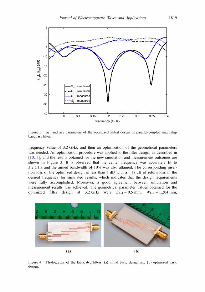
frequency value of 3.2 GHz, and then an optimization of the geometrical parameterswas needed. An optimization procedure was applied to the filter design, as described in[10,11], and the results obtained for the new simulation and measurement outcomes areshown in Figure 3. It is observed that the center frequency was accurately fit to3.2 GHz and the aimed bandwidth of 10% was also attained. The corresponding inser-tion loss of the optimized design is less than 1 dB with a −18 dB of return loss in thedesired frequency for simulated results, which indicates that the design requirementswere fully accomplished. Moreover, a good agreement between simulation andmeasurement results was achieved. The geometrical parameter values obtained for theoptimized filter design at 3.2 GHz were S1–4 = 0.5 mm, W1–4 = 1.204 mm,
3 3.05 3.1 3.15 3.2 3.25 3.3 3.35 3.4-40
-35
-30
-25
-20
-15
-10
-5
0
5
frecuency (GHz)
|s11
|, |s
21| (
dB)
S11, simulatedS21, simulatedS11, measuredS21, measured
Figure 3. S11 and S21 parameters of the optimized initial design of parallel-coupled microstripbandpass filter.
(a) (b)
Figure 4. Photographs of the fabricated filters: (a) initial basic design and (b) optimized basicdesign.
Journal of Electromagnetic Waves and Applications 1819

L1–4 = 8.48 mm, S2–3 = 1.439 mm, W2–3 = 1.626 mm, and L2–3 = 8.361 mm.Photographs of the fabricated filters are shown in Figure 4.
For this first step of the three-steps technique proposed in this paper, the physicaldimensions of the filter layout – space gap (S), width (W), and length (L) of each res-onator stage – were obtained using the transmission line theory approach that can befound in textbooks as in [12]. In [11], a calculator is introduced to automate thecalculation of these design parameters. These values will become the input for the opti-mization design tool subsequently used in this first step and indicated in [10,11].
The number of bands of the filter is related to the order of the filter; however, asshown in Figure 3, the multiband feature of the initial filter is not remarkable. Then,the following step of the proposed technique will consist of enhancing the multibandfrequency response.
3.2. Extension of the filter response to tri-band feature
On obtaining the conventional parallel-coupled microstrip bandpass filter design for thecenter frequency of 3.2 GHz, the next step was to analyze the effect on the bandpassfilter response of decreasing the coupling gap between resonators. The main objectiveof this step is to enhance the multiband feature of the filter frequency response.
By means of the CST software, we test the effect of different values of the spacinggaps S1–4 and S2–3, for sections (1–4) and (2–3), in terms of return loss and frequencyresonances. Figures 5 and 6 illustrate the parameters S11 and S21 for different values ofthe spacing gaps S1–4 and S2–3, for sections (1–4) and (2–3), respectively. In Figure 5,the curves corresponding to the return loss – |S11| in dB – demonstrate that the band-pass filter is sensitive to decrease and increases of the values adopted for S1–4 and S2–3.We observe that as a result of a coupling gap decrease, the middle band is slightly
2 2.5 3 3.5 4 4.5 5 5.5 6 6.5 7-50
-45
-40
-35
-30
-25
-20
-15
-10
-5
0
5
frequency (GHz)
|s11
|, |s
21| (
dB)
S1-4= 0.02 mmS1-4= 0.06 mmS1-4= 0.1 mm
Figure 5. S11 and S21 parameters of bandpass filter for several coupling gap values (S1–4).
1820 A. Naghar et al.
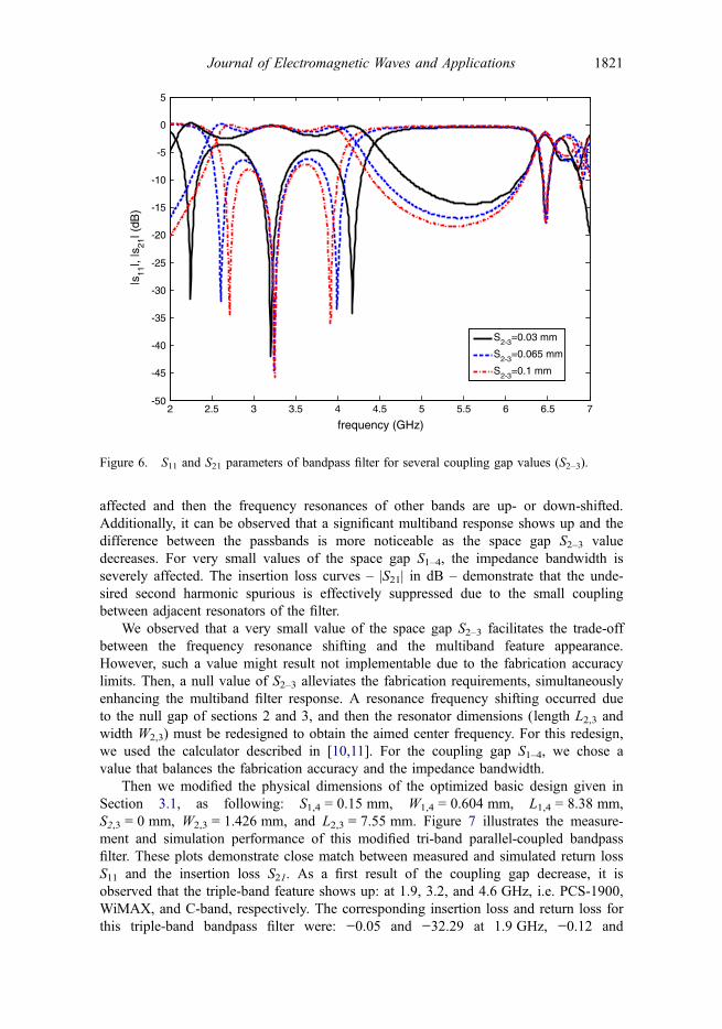
affected and then the frequency resonances of other bands are up- or down-shifted.Additionally, it can be observed that a significant multiband response shows up and thedifference between the passbands is more noticeable as the space gap S2–3 valuedecreases. For very small values of the space gap S1–4, the impedance bandwidth isseverely affected. The insertion loss curves – |S21| in dB – demonstrate that the unde-sired second harmonic spurious is effectively suppressed due to the small couplingbetween adjacent resonators of the filter.
We observed that a very small value of the space gap S2–3 facilitates the trade-offbetween the frequency resonance shifting and the multiband feature appearance.However, such a value might result not implementable due to the fabrication accuracylimits. Then, a null value of S2–3 alleviates the fabrication requirements, simultaneouslyenhancing the multiband filter response. A resonance frequency shifting occurred dueto the null gap of sections 2 and 3, and then the resonator dimensions (length L2,3 andwidth W2,3) must be redesigned to obtain the aimed center frequency. For this redesign,we used the calculator described in [10,11]. For the coupling gap S1–4, we chose avalue that balances the fabrication accuracy and the impedance bandwidth.
Then we modified the physical dimensions of the optimized basic design given inSection 3.1, as following: S1,4 = 0.15 mm, W1,4 = 0.604 mm, L1,4 = 8.38 mm,S2,3 = 0 mm, W2,3 = 1.426 mm, and L2,3 = 7.55 mm. Figure 7 illustrates the measure-ment and simulation performance of this modified tri-band parallel-coupled bandpassfilter. These plots demonstrate close match between measured and simulated return lossS11 and the insertion loss S21. As a first result of the coupling gap decrease, it isobserved that the triple-band feature shows up: at 1.9, 3.2, and 4.6 GHz, i.e. PCS-1900,WiMAX, and C-band, respectively. The corresponding insertion loss and return loss forthis triple-band bandpass filter were: −0.05 and −32.29 at 1.9 GHz, −0.12 and
2 2.5 3 3.5 4 4.5 5 5.5 6 6.5 7-50
-45
-40
-35
-30
-25
-20
-15
-10
-5
0
5
frequency (GHz)
|s11
|, |s
21| (
dB)
S2-3=0.03 mm
S2-3=0.065 mm
S2-3=0.1 mm
Figure 6. S11 and S21 parameters of bandpass filter for several coupling gap values (S2–3).
Journal of Electromagnetic Waves and Applications 1821
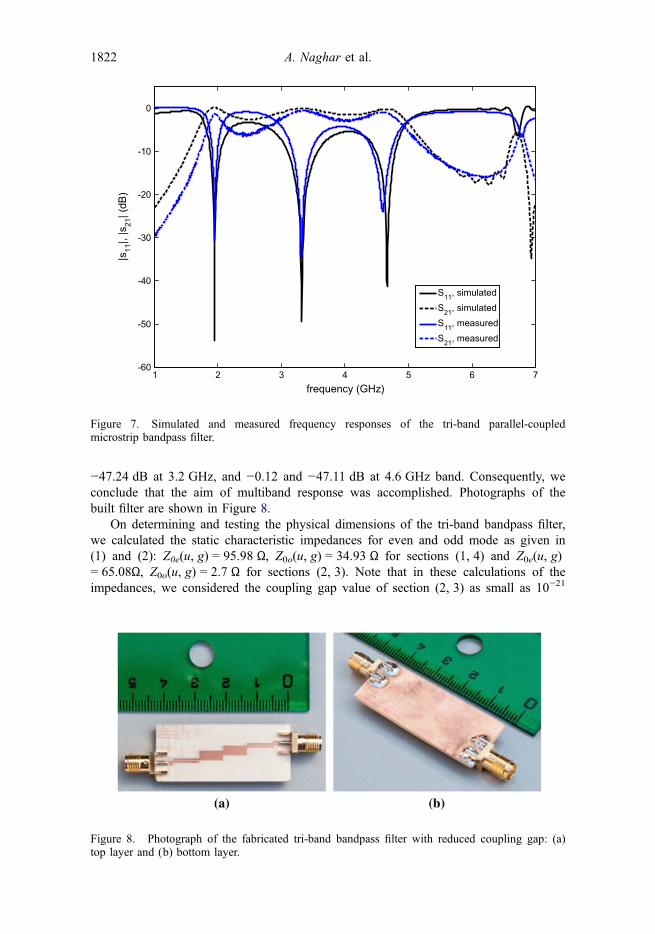
−47.24 dB at 3.2 GHz, and −0.12 and −47.11 dB at 4.6 GHz band. Consequently, weconclude that the aim of multiband response was accomplished. Photographs of thebuilt filter are shown in Figure 8.
On determining and testing the physical dimensions of the tri-band bandpass filter,we calculated the static characteristic impedances for even and odd mode as given in(1) and (2): Z0e(u, g) = 95.98 Ω, Z0o(u, g) = 34.93 Ω for sections (1, 4) and Z0e(u, g)= 65.08Ω, Z0o(u, g) = 2.7 Ω for sections (2, 3). Note that in these calculations of theimpedances, we considered the coupling gap value of section (2, 3) as small as 10−21
1 2 3 4 5 6 7-60
-50
-40
-30
-20
-10
0
frequency (GHz)
|s11
|, |s
21| (
dB)
S11, simulatedS21, simulatedS11, measuredS21, measured
Figure 7. Simulated and measured frequency responses of the tri-band parallel-coupledmicrostrip bandpass filter.
Figure 8. Photograph of the fabricated tri-band bandpass filter with reduced coupling gap: (a)top layer and (b) bottom layer.
1822 A. Naghar et al.

instead of zero to avoid the singularity. Now using these characteristic impedancesvalues along with the length of each microstrip line of the tri-band BPF, we calculatedthe matrix ABCD as in (5) and (8). Finally, the S11 and S21 parameters of the tri-bandfilter were calculated as in (9) and (10) and represented in Figure 9, showing reason-able agreement between simulation in CST, measurement, and numerical analysis bythe formulation given in Section 2 that was thus validated.
3.3. Second harmonic suppression: ground plane apertures insertion
In order to likely enhance the performance of the tri-band bandpass filter obtained inthe previous step, we implemented the classical technique of spurious response suppres-sion described in [6] that consists of inserting apertures in the ground plane. The filterlayout is shown in Figure 10, and the physical dimensions used for the apertures wereWs1 = 2W1–4 + S1–4 + 0.4 mm, Ws2 = 2W2–3 + S2–3 + 0.4 mm, Ls1 = L1–4 − 0.4 mm, andLs2 = L2–3 − 0.1 mm.
The filter performance achieved by adding apertures or slots in the ground planewas plotted in Figure 11 also showing a comparison with the case without slotsachieved in Section 3.2 (see Figure 7). It can be checked that the filter response wasminimally affected by comparison to the results presented by the filter without slots. Inaddition, it is evident from the same comparison that the second harmonic was notaffected by the insertion of ground apertures. These results demonstrate that thestructure introduced to obtain the tri-band response based on small and null couplinggap was enough to achieve not only a multiband response but also a second harmonicsuppression not worse than that given by the classical technique of ground apertures.
As above explained in Section 2.2, the spurious response was eliminated by com-pensating the difference between the phase velocities,[20] given that a small coupling
1 1.5 2 2.5 3 3.5 4 4.5 5 5.5 6-70
-60
-50
-40
-30
-20
-10
0
frequency (GHz)
|s11
|, |s
21| (
dB)
S11 simulatedS21 simulatedS11 measuredS21 measuredS11 calculatedS21 calculated
Figure 9. Simulated, measured, and calculated frequency responses of the tri-band BPF withreduced coupling gap.
Journal of Electromagnetic Waves and Applications 1823

decreases the odd-mode phase velocity. Following (13)–(17), the phase velocity fordifferent segments was calculated and the set of single values averaged. The ratiobetween odd and even phase velocities Vpo/Vpe was 1.22 for single-band filter, whilst itwas 0.956 for the triple-band filter, thus confirming that the decrease of phase velocityis related to the second harmonic suppression (Figure 12).
Finally, in Figure 13, we compared the performance enhancement in terms of S21achieved for two of the filters proposed: the basic design described in Section 3.1 andthe optimized design of the present Section 3.2. We observe that the spurious 2f0 wassignificantly reduced in the response obtained with the use of low or null value ofcoupling gap between microstrip lines. The original band around 2f0 was up-shiftedand then the spurious reduction could be considered around −5 dB, if the up-shiftedpeak is considered, or around −15 dB, if it is strictly measured at 2f0. Furthermore, the
Figure 10. Layout: (a) coupled microstrip lines and (b) ground plane apertures.
1 2 3 4 5 6 7-60
-50
-40
-30
-20
-10
0
frequency (GHz)
|S11
|, |S
21| (
dB)
S11 simulated, with apertures
S21 simulated, with apertures
S11 measured, with apertures
S21 measured, with apertures
S11 measured, without apertures
S21 measured, without apertures
Figure 11. S11 and S21 parameters of the tri-band bandpass filter with and without ground planeapertures.
1824 A. Naghar et al.

bandwidth of the tri-band filter using very low or null value of coupling gaps is widerand the 2f0 response shows narrower bandwidth compared to the initial basic filterdesigned in Section 3.1.
3.4. Analysis of band center frequency and bandwidth control
According to the results presented previously, the technique shown in this work allowsobtaining an enhanced multiband response with a number of bands related to the orderassumed for the initial parallel-coupled bandpass filter design, and it suppresses theundesirable second harmonic. By creating null gaping between resonators of the centersections, the multiband response is visibly enhanced. However, we observed that two
(a) (b)
Figure 12. Photograph of the fabricated tri-band bandpass filter with ground plane apertures: (a)top layer and (b) bottom layer.
Figure 13. Comparison of simulated and measured S21 for single-band filter, triple-band filterwithout apertures, and triple-band filter with apertures.
Journal of Electromagnetic Waves and Applications 1825
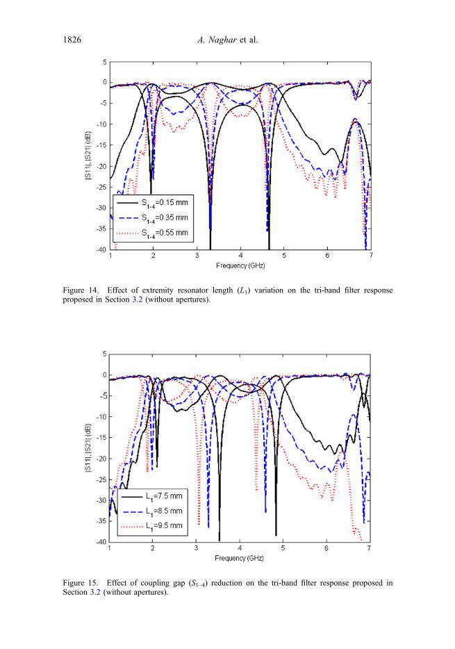
Figure 14. Effect of extremity resonator length (L1) variation on the tri-band filter responseproposed in Section 3.2 (without apertures).
Figure 15. Effect of coupling gap (S1–4) reduction on the tri-band filter response proposed inSection 3.2 (without apertures).
1826 A. Naghar et al.
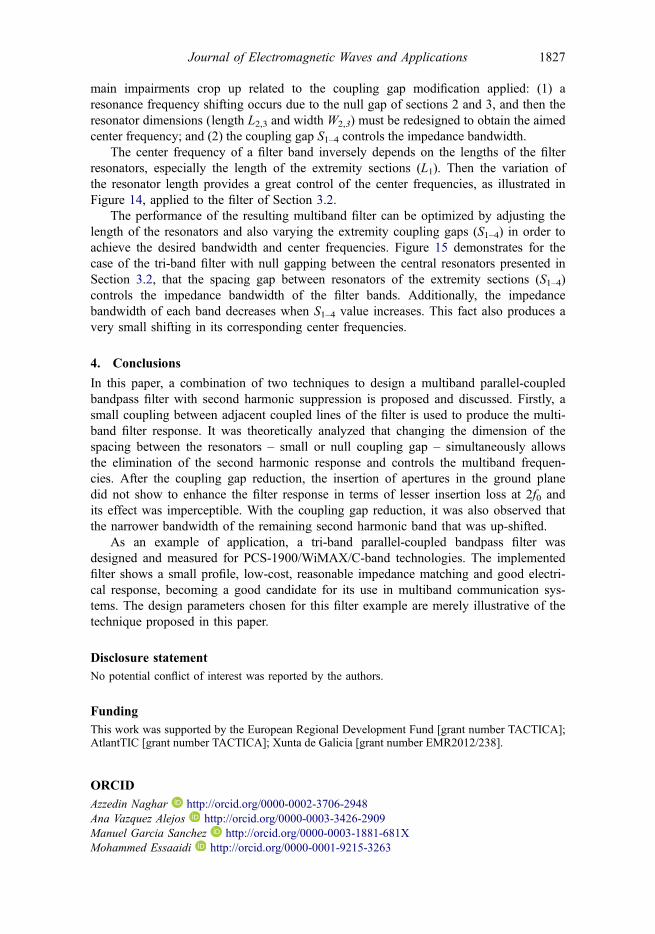
main impairments crop up related to the coupling gap modification applied: (1) aresonance frequency shifting occurs due to the null gap of sections 2 and 3, and then theresonator dimensions (length L2,3 and width W2,3) must be redesigned to obtain the aimedcenter frequency; and (2) the coupling gap S1–4 controls the impedance bandwidth.
The center frequency of a filter band inversely depends on the lengths of the filterresonators, especially the length of the extremity sections (L1). Then the variation ofthe resonator length provides a great control of the center frequencies, as illustrated inFigure 14, applied to the filter of Section 3.2.
The performance of the resulting multiband filter can be optimized by adjusting thelength of the resonators and also varying the extremity coupling gaps (S1–4) in order toachieve the desired bandwidth and center frequencies. Figure 15 demonstrates for thecase of the tri-band filter with null gapping between the central resonators presented inSection 3.2, that the spacing gap between resonators of the extremity sections (S1–4)controls the impedance bandwidth of the filter bands. Additionally, the impedancebandwidth of each band decreases when S1–4 value increases. This fact also produces avery small shifting in its corresponding center frequencies.
4. Conclusions
In this paper, a combination of two techniques to design a multiband parallel-coupledbandpass filter with second harmonic suppression is proposed and discussed. Firstly, asmall coupling between adjacent coupled lines of the filter is used to produce the multi-band filter response. It was theoretically analyzed that changing the dimension of thespacing between the resonators – small or null coupling gap – simultaneously allowsthe elimination of the second harmonic response and controls the multiband frequen-cies. After the coupling gap reduction, the insertion of apertures in the ground planedid not show to enhance the filter response in terms of lesser insertion loss at 2f0 andits effect was imperceptible. With the coupling gap reduction, it was also observed thatthe narrower bandwidth of the remaining second harmonic band that was up-shifted.
As an example of application, a tri-band parallel-coupled bandpass filter wasdesigned and measured for PCS-1900/WiMAX/C-band technologies. The implementedfilter shows a small profile, low-cost, reasonable impedance matching and good electri-cal response, becoming a good candidate for its use in multiband communication sys-tems. The design parameters chosen for this filter example are merely illustrative of thetechnique proposed in this paper.
Disclosure statementNo potential conflict of interest was reported by the authors.
FundingThis work was supported by the European Regional Development Fund [grant number TACTICA];AtlantTIC [grant number TACTICA]; Xunta de Galicia [grant number EMR2012/238].
ORCID
Azzedin Naghar http://orcid.org/0000-0002-3706-2948Ana Vazquez Alejos http://orcid.org/0000-0003-3426-2909Manuel Garcia Sanchez http://orcid.org/0000-0003-1881-681XMohammed Essaaidi http://orcid.org/0000-0001-9215-3263
Journal of Electromagnetic Waves and Applications 1827

References[1] Miyake H, Kitazawa S, Ishizaki T, Yamanda T, Nagatomi Y. A miniaturized monolithic
dual-band filter using ceramic lamination technique for dual-mode portable telephones. IEEEMTT-S Int. Microwave Symp. Dig. 1997;2:789–792.
[2] Horii Y. Passive microwave components and antennas. Rijeka, Croatia: Intech Open; 2010.Chapter 15, Design of compact planar ultra-wideband bandpass filters; p. 323–339.
[3] Macchiarella G, Tamiazzo S. Design techniques for dual-passband filters. IEEE Trans.Microwave Theory Tech. 2005;53:3265–3271.
[4] Chen CC. Dual-band bandpass filter using coupled resonator pairs. IEEE MicrowaveWireless Compon. Lett. 2005;15:259–261.
[5] Bahl IJ. Capacitively compensated high performance parallel coupled microstrip filters. IEEEM1T-S Int. Microwave Symp. Dig. 1989;2:679–682.
[6] del Castillo M, Ahumada V, Martel J, Medina F. Parallel coupled microstrip filters withground-plane aperture for spurious band suppression and en-hanced coupling. IEEE Trans.Microwave Theory Tech. 2004;52:1082–1086.
[7] Kim I, Kingsley N, Morton M, Bairavasubramanian R, Papapolymerou J, Tentzeris MM,Yook JG. Fractal-shaped microstrip coupled-line band pass filters for suppression of secondharmonic. IEEE. Trans. Microwave Theory Tech. 2005;53:2943–2948.
[8] Moradian M, Tayarani M. Spurious-response suppression in microstrip parallel-coupledbandpass Filters by grooved substrates. IEEE. Trans. Microwave Theory Tech.2008;56:1707–1713.
[9] Alaydrus M. Designing microstrip bandpass filter at 3.2 GHz. Int. J. Electr. Eng. Inf.2010;2:71–83.
[10] Naghar A, Aghzout O, Medina F, Alaydrus M, Essaidi M. Study and design of a compactparallel coupled microstrip band-pass filter for a 5 GHz unlicensed Mobile Wimax networks.Int. J. Sci. Technol. 2013;2:492–497.
[11] Naghar A, Aghzout O, Alejos A, Sanchez M, Essaidi M. Development of a calculator foredge and parallel coupled microstrip band pass filters. In: IEEE International Symposium onAntennas and Propagation APS-URSI 2014, July 6-12; Memphis, Tennessee, USA,p. 2018–2019.
[12] Pozar DM. Microwave engineering. fourth ed. Hoboken, NJ: Wiley; 2012.[13] Akhtarzad S, Rowbotham TR, Johns PB. The design of coupled microstrip lines. IEEE
Trans. Microwave Theory Tech. 1975;23:486–492.[14] Hammerstad E, Jensen O. Accurate models for microstrip computer-aided design. Symp.
Microwave Theory Tech. 1980;5:407–409.[15] Kirschning M, Jansen RH. Accurate wide-range design equations for the frequency
dependent characteristic of parallel coupled microstrip lines. IEEE. Trans. MicrowaveTheory Tech. 1984;32:83–90.
[16] Kirschning M, Jansen RH. Accurate wide-range design equations for the frequency-dependent characteristics of parallel coupled microstrip lines (corrections). IEEE Trans.Microwave Theory Tech. 1985;32:83–90.
[17] Ye CS, Su YK, Weng MH, Hung CY, Yang RY. Design of the compact parallel-coupledlines wideband bandpass filters using image parameter method. Prog. Electromagn. Res.2010;100:153–173.
[18] Chin K-S, Kuo J-T. Insertion loss function synthesis of maximally flat parallel-coupled linebandpass filters. IEEE Trans. Microwave Theory Tech. 2005;53:3161–3168.
[19] Chin K-S, Chiou Y-C, Kuo J-T. New synthesis of parallel-coupled line bandpass filters WithChebyshev responses. IEEE. Trans. Microwave Theory Tech. 2008;56:1516–1523.
[20] Coonrod J. Harmonic suppression of edge coupled filters using composite substrates.Microwave J. 2012;55:104–114.
[21] Sheleg B, Spielman BE. Characteristics of coupled microstriplines. IEEE. Trans. MicrowaveTheory Tech. 2005;32:83–89.
1828 A. Naghar et al.

5. M. Kelley, C. Koo, H. McQuilken, B. Lawrence, S. Li, A. Han, and
G. Huff, Frequency reconfigurable patch antenna using liquid metal
as switching mechanism, Electron Lett 49 (2013), 1370–1371.
6. R. Raj, B. Poussot, J.M. Laheurte, and O. Vendier, Pattern reconfi-
guration of microstrip antenna using flip-chip mounted packaged
MEMS, Microwave Opt Technol Lett 52 (2010), 574–577.
7. O.H. Karabey, S. Bildik, S. Bausch, S. Strunck, A. Gaebler, and R.
Jakoby, Continuously polarization agile antenna by using liquid
crystal-based tunable variable delay lines, IEEE Trans Antennas
Propag 61 (2013), 70–76.
8. S. Nikolaou, R. Bairavasubramanian, C. Lugo, I. Carrasquillo, G.E.
Ponchark, J. Papapolymerou, and M.M. Tentzers, Pattern and fre-
quency reconfigurable annular slot antenna using PIN diodes, IEEE
Trans Antennas Propag 54 (2006), 439–448.
9. D. Rodrigo and L. Jofre, Frequency and radiation pattern reconfigur-
ability of a multi-size pixel antenna, IEEE Trans Antennas Propag
60 (2012), 2219–2225.
10. H. Liu, S. Gao, and T.H. Loh, Compact MIMO antenna with fre-
quency reconfigurability and adaptive radiation patterns, IEEE
Antennas Wireless Propag Lett 12 (2013), 269–272.
VC 2015 Wiley Periodicals, Inc.
COMPACT MICROSTRIPOMNIDIRECTIONAL ULTRAWIDEBANDANTENNA WITH DUAL BROADBANDNESTED U-SHAPED SLOTS AND FLATFREQUENCY RESPONSE
A. Naghar,1 A. V. Alejos,2 O. Aghzout,1 and M. Essaidi31 Faculty of Science, Abdelmalek Essaadi University, Tetouan,Morocco2 Department of Teorıa De La Se~nal Y Comunicacion, University ofVigo, Pontevedra, Vigo, Spain; Corresponding author:[email protected] School of Computer Science and Systems Analysis, Mohamed V-Souissi University, Rabat, Morocco
Received 29 April 2015
ABSTRACT: In this article, we present a compact ultrawidebandantenna with dual broadband-notched characteristics centered at 3.4
and 5.5 GHz. The proposed antenna consists of a rectangular patch witha modified ground plane structure and 50 X microstrip-fed line. By etch-ing two opposite U-shaped slots in the radiating patch, the notched
bands of 3.375–3.945 GHz for WiMAX and 5.425–6.150 GHz for WLANand HYPERLAN/2 were achieved. The antenna also offers a flat fre-
quency response so minimizing the formation of spurs and precursorsthat ensures optimal time domain performance for ultrawideband radioapplications. The return loss was measured to better than 210 dB over
the entire band from 3.1 to 10.6 GHz. The antenna gain was larger than2 dBi all over the frequencies with a flatness of 2.5 dB and an omnidir-
ectional radiation pattern in the H-plane. VC 2015 Wiley Periodicals, Inc.
Microwave Opt Technol Lett 57:2854–2856, 2015; View this article
online at wileyonlinelibrary.com. DOI 10.1002/mop.29460
Key words: antenna; ultrawideband; notch; dispersive propagation
1. INTRODUCTION
The antenna is one of the components which have experienced a
significant research increase in the recent years since that the
United State Federal Communications Commission disclosure the
ultrawideband (UWB) communication band from 3.1 to 10.6 GHz
for commercial use. Besides many challenges related to the UWB
antenna design—from the impedance matching to the compact
size and low cost—over the UWB band there exist some narrow-
band wireless communication systems which might interfere to
the UWB systems: IEEE 802.16 WiMAX, operating at the 3.3–
3.7 GHz band, and IEEE 802.11a WLAN, operating at the
5.15–5.85 GHz band, and HYPERLAN/2 at the 5.425–6.150 GHz
band.
Several antenna design methods have been proposed to pro-
duce the band-rejection in the UWB band. Among other
approaches, providing UWB antennas with band-notched char-
acteristic is necessary to solve this emerging problem of nar-
rowband interference [1–3]. In this article, we propose a
printed microstrip U-shaped UWB antenna with dual band-
notched configured for the bands of 3.375–3.945 GHz
(WiMAX) and 5.425–6.150 GHz (HYPERLAN/2 and WLAN).
The geometry of the achieved UWB antenna design is simple
with compact size and fewer critical parameters. This novel
structure consists of combining a rectangular patch with micro-
strip line feeding with a modified ground plane. The dual
band-notched operation is achieved by etching two nested
U-shaped slots in the rectangular metal radiating patch. By
fine-tuning the width and the total length of each U-shaped
slot, the notch center frequency and bandwidth can be, respec-
tively, controlled.
The dual-band notched design showed an omnidirectional
radiation pattern, and the antenna gain obtained a flatness of 2
dB. Finally, the time domain analysis of the antenna indicated a
response which diminishes the formation of precursor fields [4]
superimposed to the transmitted signal.
Figure 1 UWB antenna with dual band-notched characteristics: (a)
Geometry of the antenna with detail of ground plane. (b) Photo of the
fabricated prototypes. [Color figure can be viewed in the online issue,
which is available at wileyonlinelibrary.com]
2854 MICROWAVE AND OPTICAL TECHNOLOGY LETTERS / Vol. 57, No. 12, December 2015 DOI 10.1002/mop
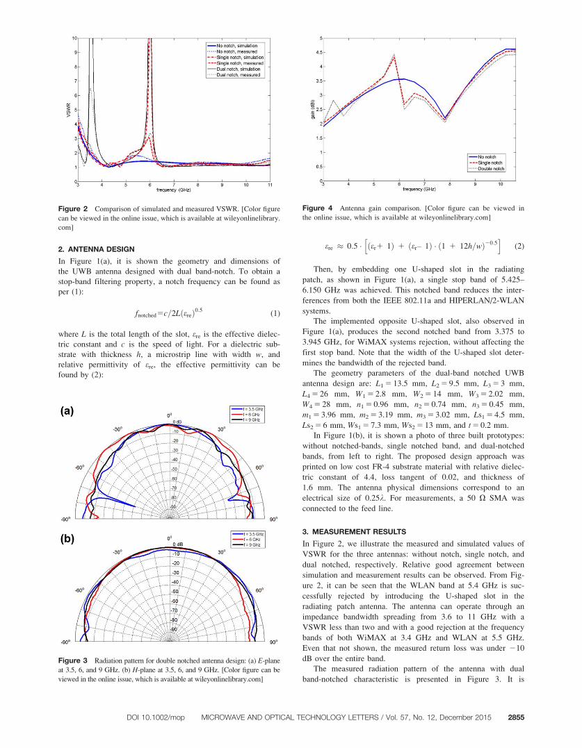
2. ANTENNA DESIGN
In Figure 1(a), it is shown the geometry and dimensions of
the UWB antenna designed with dual band-notch. To obtain a
stop-band filtering property, a notch frequency can be found as
per (1):
fnotched5c=2L ereð Þ0:5 (1)
where L is the total length of the slot, ere is the effective dielec-
tric constant and c is the speed of light. For a dielectric sub-
strate with thickness h, a microstrip line with width w, and
relative permittivity of ere, the effective permittivity can be
found by (2):
ere 0:5 er1 1ð Þ 1 er– 1ð Þ 1 1 12h=wð Þ20:5h i
(2)
Then, by embedding one U-shaped slot in the radiating
patch, as shown in Figure 1(a), a single stop band of 5.425–
6.150 GHz was achieved. This notched band reduces the inter-
ferences from both the IEEE 802.11a and HIPERLAN/2-WLAN
systems.
The implemented opposite U-shaped slot, also observed in
Figure 1(a), produces the second notched band from 3.375 to
3.945 GHz, for WiMAX systems rejection, without affecting the
first stop band. Note that the width of the U-shaped slot deter-
mines the bandwidth of the rejected band.
The geometry parameters of the dual-band notched UWB
antenna design are: L1 5 13.5 mm, L2 5 9.5 mm, L3 5 3 mm,
L4 5 26 mm, W1 5 2.8 mm, W2 5 14 mm, W3 5 2.02 mm,
W4 5 28 mm, n1 5 0.96 mm, n2 5 0.74 mm, n3 5 0.45 mm,
m1 5 3.96 mm, m2 5 3.19 mm, m3 5 3.02 mm, Ls1 5 4.5 mm,
Ls2 5 6 mm, Ws1 5 7.3 mm, Ws2 5 13 mm, and t 5 0.2 mm.
In Figure 1(b), it is shown a photo of three built prototypes:
without notched-bands, single notched band, and dual-notched
bands, from left to right. The proposed design approach was
printed on low cost FR-4 substrate material with relative dielec-
tric constant of 4.4, loss tangent of 0.02, and thickness of
1.6 mm. The antenna physical dimensions correspond to an
electrical size of 0.25k. For measurements, a 50 X SMA was
connected to the feed line.
3. MEASUREMENT RESULTS
In Figure 2, we illustrate the measured and simulated values of
VSWR for the three antennas: without notch, single notch, and
dual notched, respectively. Relative good agreement between
simulation and measurement results can be observed. From Fig-
ure 2, it can be seen that the WLAN band at 5.4 GHz is suc-
cessfully rejected by introducing the U-shaped slot in the
radiating patch antenna. The antenna can operate through an
impedance bandwidth spreading from 3.6 to 11 GHz with a
VSWR less than two and with a good rejection at the frequency
bands of both WiMAX at 3.4 GHz and WLAN at 5.5 GHz.
Even that not shown, the measured return loss was under 210
dB over the entire band.
The measured radiation pattern of the antenna with dual
band-notched characteristic is presented in Figure 3. It is
Figure 3 Radiation pattern for double notched antenna design: (a) E-plane
at 3.5, 6, and 9 GHz. (b) H-plane at 3.5, 6, and 9 GHz. [Color figure can be
viewed in the online issue, which is available at wileyonlinelibrary.com]
Figure 4 Antenna gain comparison. [Color figure can be viewed in
the online issue, which is available at wileyonlinelibrary.com]Figure 2 Comparison of simulated and measured VSWR. [Color figure
can be viewed in the online issue, which is available at wileyonlinelibrary.
com]
DOI 10.1002/mop MICROWAVE AND OPTICAL TECHNOLOGY LETTERS / Vol. 57, No. 12, December 2015 2855

observed an omnidirectional performance in the H-plane, and a
like-small dipole in the E-plane.
Finally, in Figure 4 it is shown a comparison of the antenna
gain for the three built prototypes: the gain is over 2 dBi for the
entire band with a deviation of 2.5 dB for the three cases, so
resulting in a flat frequency response, considering the ratio of
gain flatness versus bandwidth.
4. TIME DOMAIN ANALYSIS
As described in [5], the S21(f) parameter of the antenna was esti-
mated and used to analyze the distortion on a transmitted pulse.
The evolution of a signal x(t) transmitted through the antenna
can be evaluated in the frequency domain as in (3):
yðtÞ5 IFT fs21ðf Þ X fð Þg (3)
where IFT denotes the inverse Fourier transform, and X(f) is the
input signal in the spectrum domain. The input signal consisted
of a baseband pulse modulating a sine carrier with frequency
f0 5 7.5 GHz.
In Table 1, we show the value of the correlation factor in
percentage estimated between the original signals fed into the
antenna and the signal obtained after transmission calculated as
in (1). Four different baseband pulses commonly found in UWB
applications have been analyzed for three durations of the pulse
time width Tb—inversely related to the pulse bandwidth—meas-
ured in terms of 1/f0. The q values are given in triplets corre-
sponding to the three antenna cases.
The larger input pulse bandwidth, more critical becomes the
effect of the frequency dispersion induced by the antenna on the
input pulse mainly due to the emergence of the precursor field,
and then the correlation factor q decreases considerably. The
distortion undergone as a result of the formation of precursor
fields derived of the frequency dependence of the antenna trans-
fer function observed in the response s21(f).The most favorable case, almost distortion free, is obtained
for the Lorentz pulse given to the lower amplitude level reached
by the precursor field formed during the transmission of this sig-
nal that can be explained by the smooth edges of the pulse. The
worst case was achieved for the impulse pulse—configured as a
delta function—due to present a frequency bandwidth as large
as the entire band so emphasizing the effects of the frequency
dispersion induced by the antenna response and maximizing the
precursor field formation.
The plot shown in Figure 5 better illustrates the Brillouin
precursor formation. We plotted the case of the sine carrier
modulated rectangular pulse once propagated through the
antenna transfer function. The precursors appear superimposed
on the leading and trailing edges of the output pulse. We com-
pared the performance for each of the three antennas: as larger
the precursor peak, more frequency dispersive results to be the
antenna; however, even that the dual-notch antenna shows fre-
quency flatness, it introduces a slight distortion in the intermedi-
ate cycles of the carrier due to the frequency notches, as
observed p.e. in the gain comparison of Figure 4.
5. CONCLUSION
In this article, a compact printed UWB antenna with dual-band
notched characteristic has been proposed. To produce dual-band
rejection, two nested U-shaped slots are embedded in the radiat-
ing patch antenna so creating two stop-band filters with center
frequencies of 3.4 and 5.5 GHz. According to the results, the
proposed antenna achieves a performance similar to other results
[6] in terms of antenna gain and VSWR; however the proposed
design obtains benefits in terms of flat-frequency response and
omnidirectional radiation pattern in the H-plane. The time
domain analysis indicates dependence with the transmitted pulse
shape and its setting.
ACKNOWLEDGMENTS
Research supported by the Xunta de Galicia (Grant EMR2012/
138), Erasmus Mundus Green IT (Grant 2012-2625/001-001-
EMA2), AtlantTic Research Center and European Regional
Development Fund (ERDF).
REFERENCES
1. L. Luo, Z. Cui, J.P. Xiong, X.M. Zhang, and Y.C. Jiao, Compact
printed ultra-wideband monopole antenna with dual band-notch char-
acteristic, IET Electron Lett 44 (2001), 1106–1107.
2. Q.-X. Chu and Y.Y. Yang, A compact ultrawideband antenna with
3.4/5.5GHz dual band-notched characteristics, IEEE Trans Antennas
Propag 56 (2008), 3637–3644.
3. J. Zang and X. Wang, A compact C-shaped printed UWB antenna
with band-notched characteristics, Prog Electromagn Res Lett 43
(2013), 15–23.
4. M. Dawood, H.U.R. Mohammed, and A.V. Alejos, Experimental
detection of Brillouin precursors through tap water at microwave fre-
quencies, IET Electron Lett 46 (2010), 1645–1647.
5. J.R. Costa, C.R. Medeiros, and C.A. Fernandes, Performance of a
crossed exponentially tapered slot antenna for UWB systems, IEEE
Trans Antennas Propag 57 (2009), 1345–1352.
6. K.L. Min, J.W. Zang, and W.L. Song, UWB Antenna Blocks Inter-
ference, Microwaves RF 5 (2013), 1–6.
VC 2015 Wiley Periodicals, Inc.
TABLE 1 Variation of Correlation Factor in Percentage Withthe Transmitted Pulse Shape and Setting
Pulse q (%), Tb 5 10/fc q (%), Tb 5 5/fc q (%), Tb 5 1/fc
Lorentz
0.5/[11(t/Tb)2]
93, 94, 95 80, 82, 83 22, 27, 32
Impulse
d(t20.125 Tb)
<10, <10, <10 <10, <10, <10 <10, <10, <10
Exponential
exp[22 t/Tb]
74, 80, 85 55, 63, 70 21, 26, 31
Rectangular P(t/Tb) 81, 86, 89 66, 74, 80 33, 41, 49
Figure 5 Rectangular pulse transmitted by each of three antennas with
detection of the Brillouin precursor formation. [Color figure can be
viewed in the online issue, which is available at wileyonlinelibrary.com]
2856 MICROWAVE AND OPTICAL TECHNOLOGY LETTERS / Vol. 57, No. 12, December 2015 DOI 10.1002/mop