development of low power phase-locked loop (pll) and pll ... · phase-locked loop (pll) and...
TRANSCRIPT
Development of low power Phase-Locked Loop (PLL) and PLL-based serial transceiverPhD student Jakub Moroń,PhD student Mirosław Firlej,Dr Marek Idzik
Faculty of Physics and Applied Computer ScienceAGH University of Science and Technology
27 September 2011, Vienna
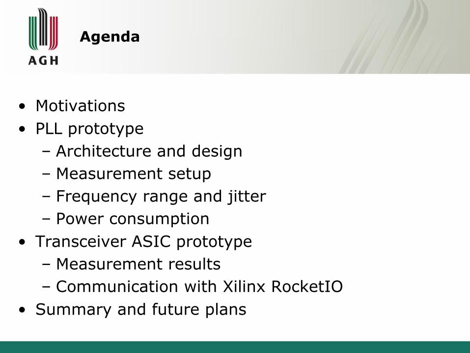
• Motivations• PLL prototype
– Architecture and design– Measurement setup– Frequency range and jitter– Power consumption
• Transceiver ASIC prototype– Measurement results– Communication with Xilinx RocketIO
• Summary and future plans
Agenda
Motivations
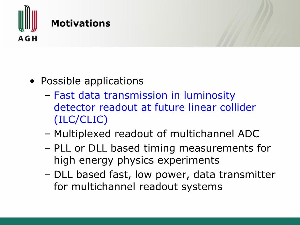
• Possible applications– Fast data transmission in luminosity
detector readout at future linear collider (ILC/CLIC)
– Multiplexed readout of multichannel ADC– PLL or DLL based timing measurements for
high energy physics experiments– DLL based fast, low power, data transmitter
for multichannel readout systems
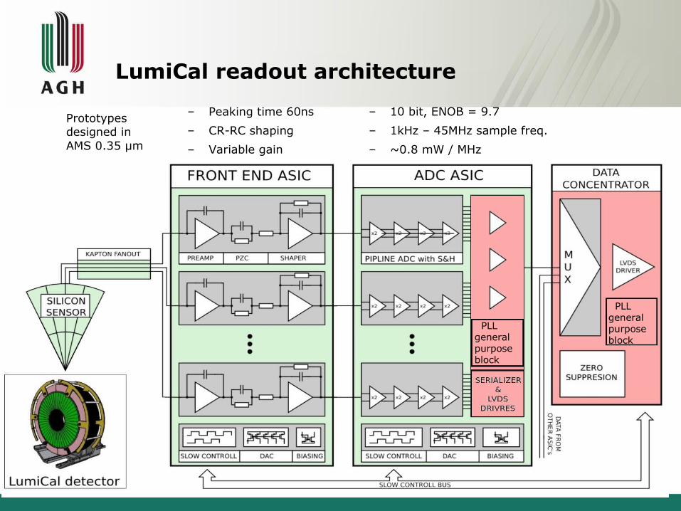
LumiCal readout architecture
Prototypes designed in AMS 0.35 μm
– 10 bit, ENOB = 9.7
– 1kHz – 45MHz sample freq.
– ~0.8 mW / MHz
– Peaking time 60ns
– CR-RC shaping
– Variable gain
PLL general purpose block
PLL general purpose block
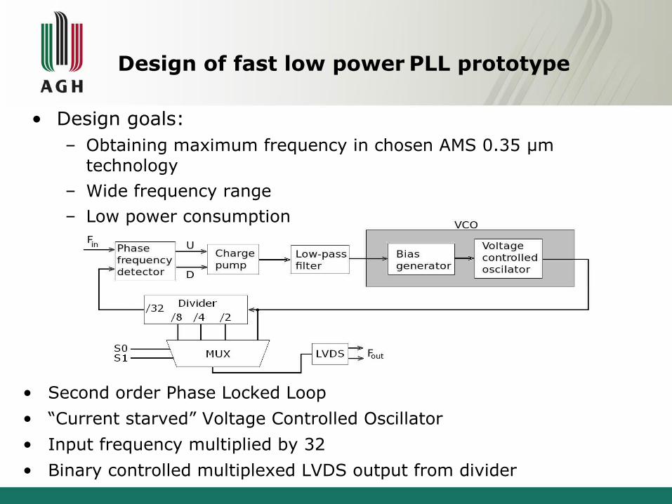
Design of fast low power PLL prototype
• Second order Phase Locked Loop
• “Current starved” Voltage Controlled Oscillator
• Input frequency multiplied by 32
• Binary controlled multiplexed LVDS output from divider
• Design goals:– Obtaining maximum frequency in chosen AMS 0.35 μm
technology– Wide frequency range– Low power consumption
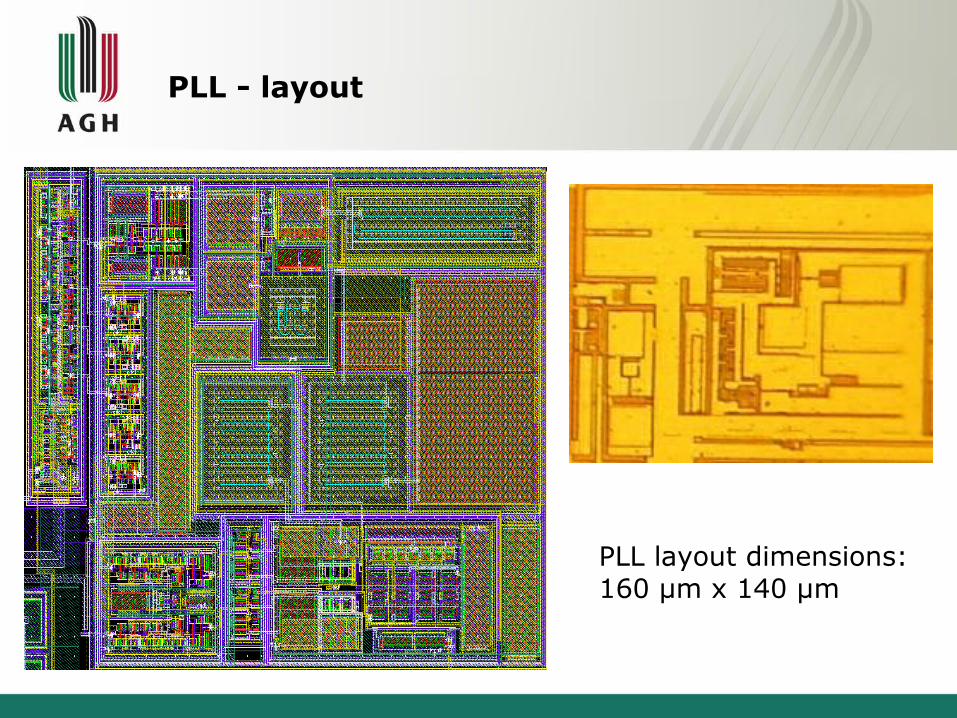
PLL - layout
PLL layout dimensions: 160 μm x 140 μm
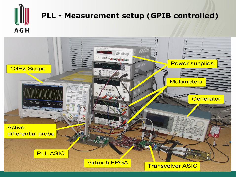
PLL - Measurement setup (GPIB controlled)
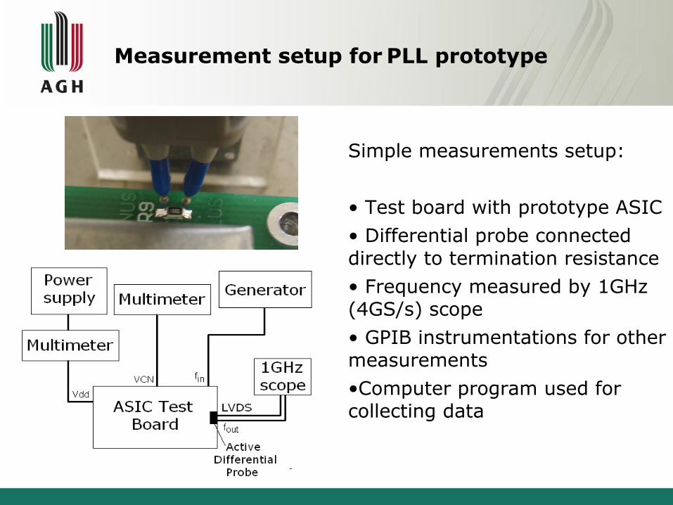
Measurement setup for PLL prototype
Simple measurements setup:
• Test board with prototype ASIC
• Differential probe connected directly to termination resistance• Frequency measured by 1GHz (4GS/s) scope
• GPIB instrumentations for other measurements•Computer program used for collecting data
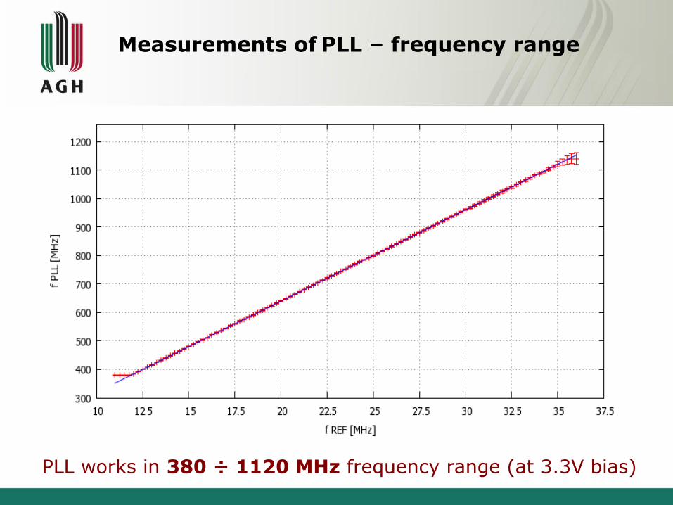
Measurements of PLL – frequency range
PLL works in 380 ÷ 1120 MHz frequency range (at 3.3V bias)
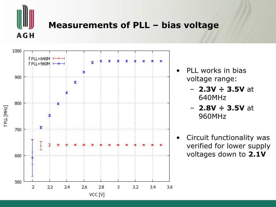
Measurements of PLL – bias voltage
• PLL works in bias voltage range:
– 2.3V ÷ 3.5V at 640MHz
– 2.8V ÷ 3.5V at 960MHz
• Circuit functionality was verified for lower supply voltages down to 2.1V
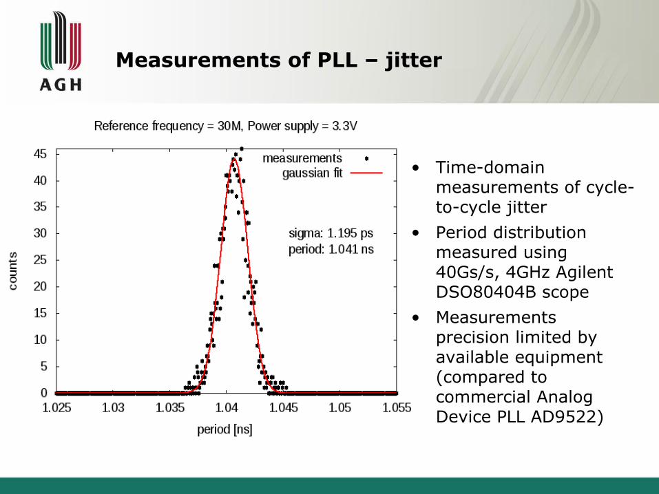
Measurements of PLL – jitter
• Time-domain measurements of cycle-to-cycle jitter
• Period distribution measured using 40Gs/s, 4GHz Agilent DSO80404B scope
• Measurements precision limited by available equipment (compared to commercial Analog Device PLL AD9522)
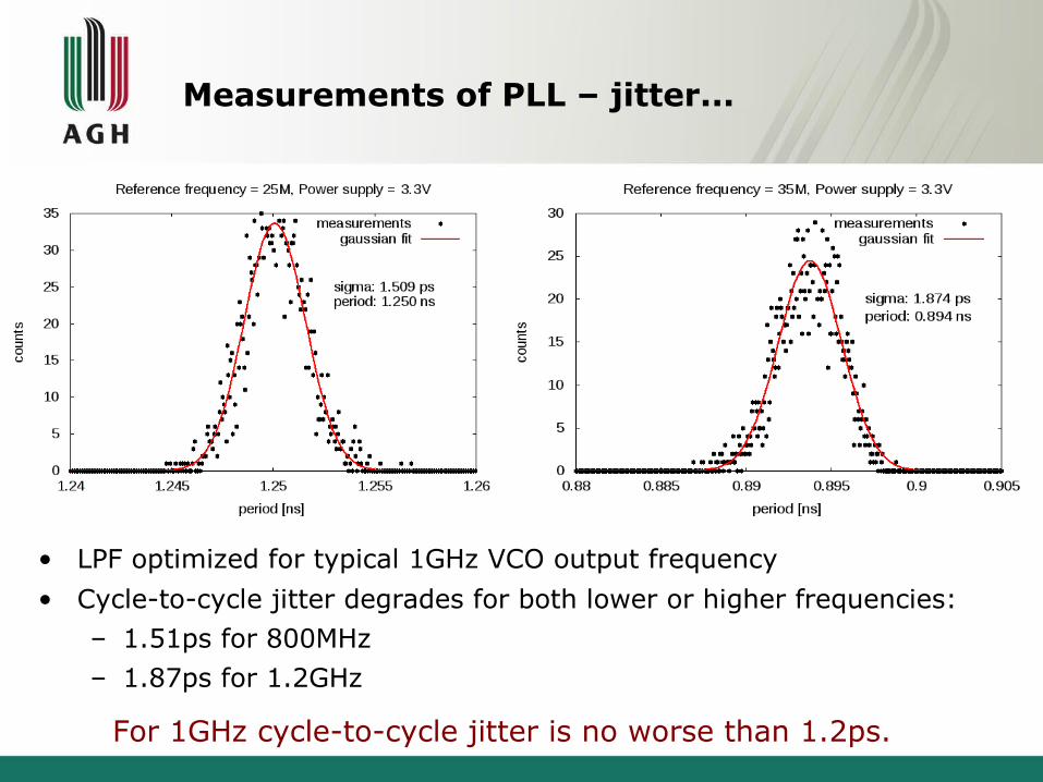
Measurements of PLL – jitter...
• LPF optimized for typical 1GHz VCO output frequency
• Cycle-to-cycle jitter degrades for both lower or higher frequencies:– 1.51ps for 800MHz – 1.87ps for 1.2GHz
For 1GHz cycle-to-cycle jitter is no worse than 1.2ps.
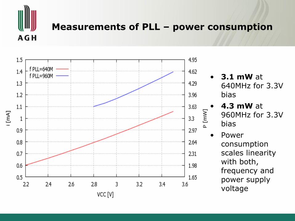
Measurements of PLL – power consumption
• 3.1 mW at 640MHz for 3.3V bias
• 4.3 mW at 960MHz for 3.3V bias
• Power consumption scales linearity with both, frequency and power supply voltage
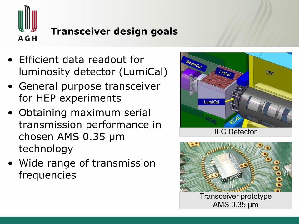
Transceiver design goals
• Efficient data readout for luminosity detector (LumiCal)
• General purpose transceiver for HEP experiments
• Obtaining maximum serial transmission performance in chosen AMS 0.35 μm technology
• Wide range of transmission frequencies
Transceiver prototypeAMS 0.35 μm
ILC Detector
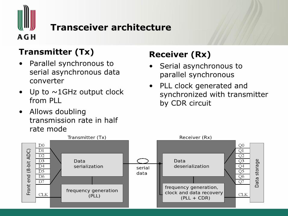
Transceiver architecture
Transmitter (Tx)• Parallel synchronous to
serial asynchronous data converter
• Up to ~1GHz output clock from PLL
• Allows doubling transmission rate in half rate mode
Receiver (Rx)• Serial asynchronous to
parallel synchronous
• PLL clock generated and synchronized with transmitter by CDR circuit
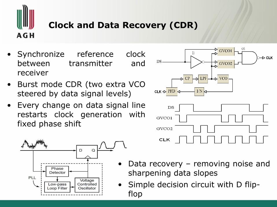
Clock and Data Recovery (CDR)
• Synchronize reference clock between transmitter and receiver
• Burst mode CDR (two extra VCO steered by data signal levels)
• Every change on data signal line restarts clock generation with fixed phase shift
• Data recovery – removing noise and sharpening data slopes
• Simple decision circuit with D flip-flop
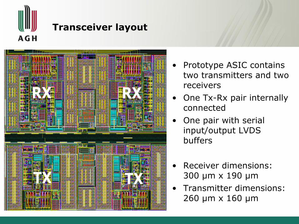
Transceiver layout
• Prototype ASIC contains two transmitters and two receivers
• One Tx-Rx pair internally connected
• One pair with serial input/output LVDS buffers
• Receiver dimensions: 300 μm x 190 μm
• Transmitter dimensions: 260 μm x 160 μm
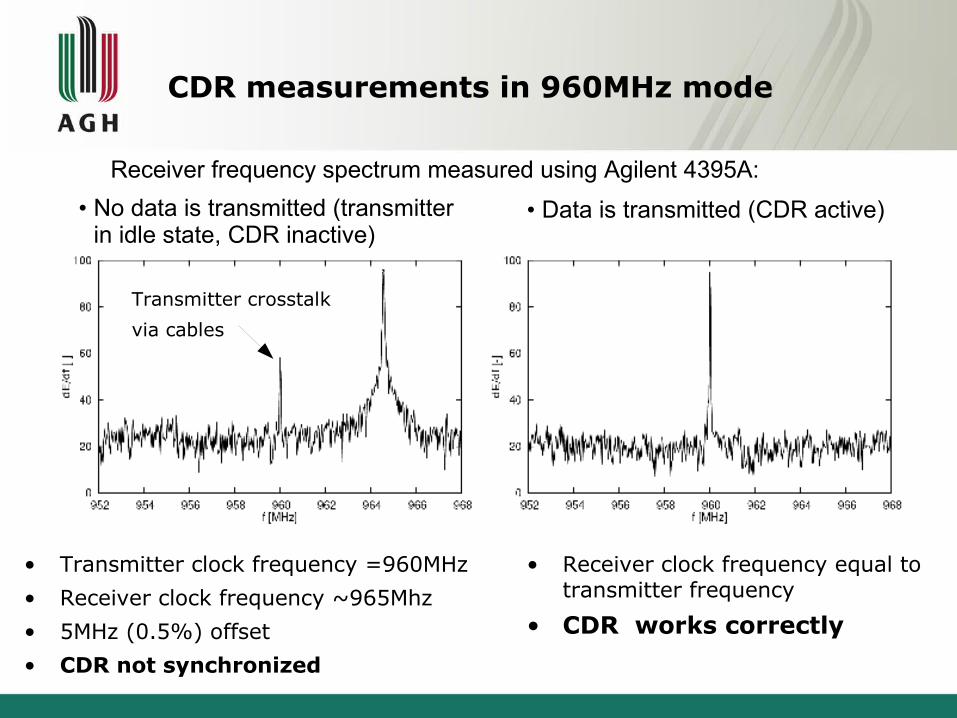
CDR measurements in 960MHz mode
• No data is transmitted (transmitter in idle state, CDR inactive)
• Data is transmitted (CDR active)
• Transmitter clock frequency =960MHz
• Receiver clock frequency ~965Mhz
• 5MHz (0.5%) offset
• CDR not synchronized
• Receiver clock frequency equal to transmitter frequency
• CDR works correctly
Transmitter crosstalk
via cables
Receiver frequency spectrum measured using Agilent 4395A:
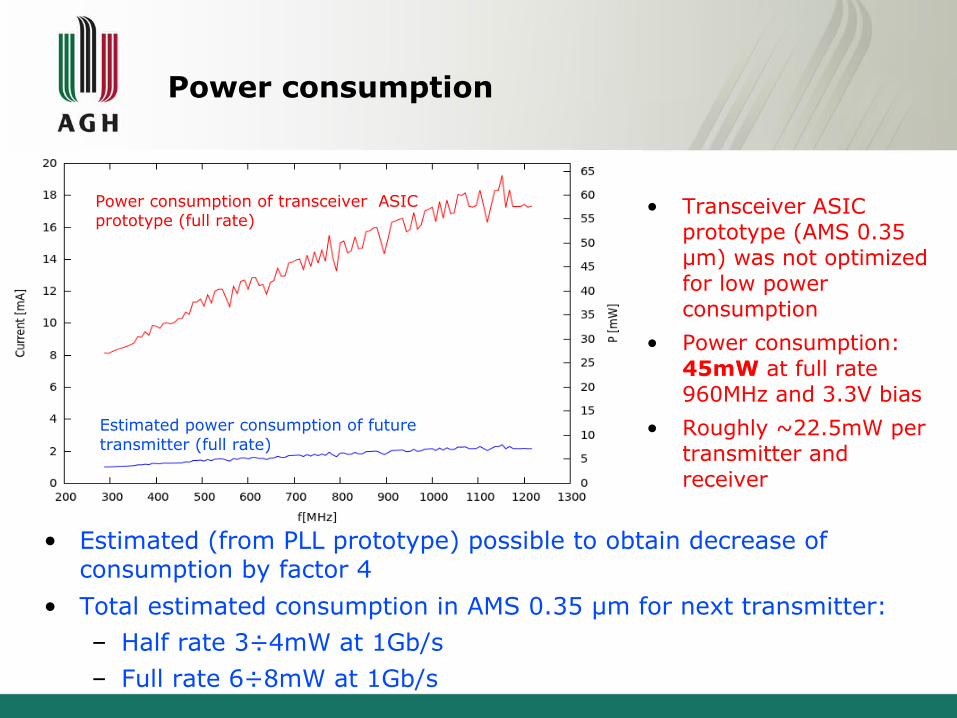
Power consumption
• Transceiver ASIC prototype (AMS 0.35 μm) was not optimized for low power consumption
• Power consumption: 45mW at full rate 960MHz and 3.3V bias
• Roughly ~22.5mW per transmitter and receiver
• Estimated (from PLL prototype) possible to obtain decrease of consumption by factor 4
• Total estimated consumption in AMS 0.35 μm for next transmitter: – Half rate 3÷4mW at 1Gb/s– Full rate 6÷8mW at 1Gb/s
Power consumption of transceiver ASIC prototype (full rate)
Estimated power consumption of future transmitter (full rate)
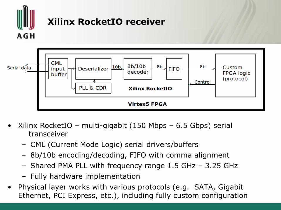
• Xilinx RocketIO – multi-gigabit (150 Mbps – 6.5 Gbps) serial transceiver
– CML (Current Mode Logic) serial drivers/buffers– 8b/10b encoding/decoding, FIFO with comma alignment
– Shared PMA PLL with frequency range 1.5 GHz – 3.25 GHz
– Fully hardware implementation
• Physical layer works with various protocols (e.g. SATA, Gigabit Ethernet, PCI Express, etc.), including fully custom configuration
Xilinx RocketIO receiver
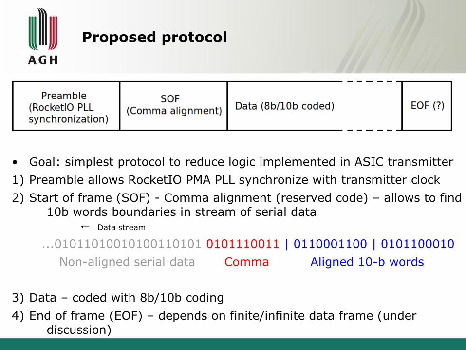
• Goal: simplest protocol to reduce logic implemented in ASIC transmitter
1) Preamble allows RocketIO PMA PLL synchronize with transmitter clock
2) Start of frame (SOF) - Comma alignment (reserved code) – allows to find 10b words boundaries in stream of serial data ← Data stream
...01011010010100110101 0101110011 | 0110001100 | 0101100010
Non-aligned serial data Comma Aligned 10-b words
3) Data – coded with 8b/10b coding
4) End of frame (EOF) – depends on finite/infinite data frame (under discussion)
Proposed protocol
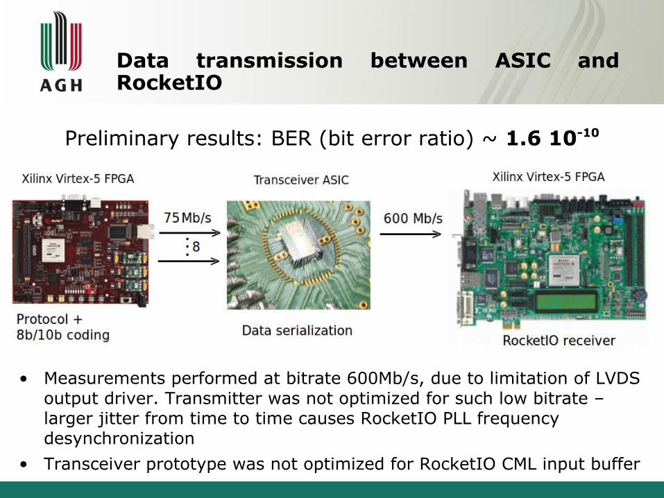
Data transmission between ASIC and RocketIO
• Measurements performed at bitrate 600Mb/s, due to limitation of LVDS output driver. Transmitter was not optimized for such low bitrate – larger jitter from time to time causes RocketIO PLL frequency desynchronization
• Transceiver prototype was not optimized for RocketIO CML input buffer
Preliminary results: BER (bit error ratio) ~ 1.6 10-10
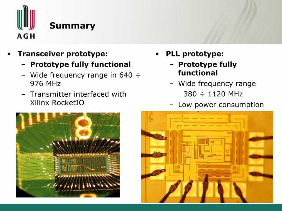
Summary
• Transceiver prototype:
– Prototype fully functional
– Wide frequency range in 640 ÷ 976 MHz
– Transmitter interfaced with Xilinx RocketIO
• PLL prototype:
– Prototype fully functional
– Wide frequency range380 ÷ 1120 MHz
– Low power consumption4.3mW at 960 MHz
Future plans
• Short term plans:
– DLL based transmitter for multichannel ADC in AMS 0.35 μm
– Low power fast (about 1GHz) transmitter in AMS 0.35 μm for LumiCal data transmission
– Ultra low power PLL in IBM 0.13 μm for new multichannel SAR ADC
• Longer term plans:
– Very low power / very fast transmitter in smaller size technology (promising candidate IBM 0.13 μm)
– PLL, DLL designs for others applications (TDC, ...)
Thank You for your attention