,.devices fax-on-demand hotline - analog.com · minimizing microprocessor wait states. the pm-7543...
TRANSCRIPT

ANALOG DEVICES fAX-ON-DEMAND HOTLINE - Page 1~
,. ANALOGW DEVICES
I
FEATURES
. Fast, Flexible Microprocessor Interface with Serial DataInput. Superior Accuracy
:t1/2 LSB INLMax:t1 LSB Gain Error MaxLow 5ppml"C Max Tempco
. Improved ESD Resistance. Auto-Insertable DIPPackage
. Surface Mount SOL Package. Superior Direct Replacement for AD7543
. -40°C to +85°C for the Extended Industrial TemperatureRange
. Available In Die Form
APPLICATIONS
. Process Control and Industrial Automation
. ProgrammableAmplifiers~ Digitally-Controlled Power Supplies, Attenuators, Filters. Instrumentation. Avionics. Auto-Calibration Systems
ORDERING INFORMATIONtTEMPERATURE RANGE
EXTENDEDttf
INDUSTRIAL COMMERCIAL
PM7543EO
GAINERROR
.i:1LSB:t2LSB.i:2LSB.i:2LSB
.i:2LSB
.i:2LSB
NON-UNEARITY MILITARY.
:l:112LSB PM7543AO:l:1/2LSB
:t1LSB:l:1lSB:l:1lSB:l:1LSB
PM7543GP
PM7543FO
PM7S43FP
PM7543FS
PM7543FPC
PM7543BO
PM7543BRC/883
. FordevicesprocessedintotalcompliancetoMIL-STD-883.add/883afler part
number. Consultlactory lor /883 data sheet.
I Burn.in isavailable on commercia! and industrial temperature range parts in
CarDIP. plastic DIP. and TO-can packages-
1T For availabilityand burn-ininformationon SO and PlCC packages. contact
your local sales office.
ttt CerDIP and epoxy devices are available in the exlended industrial tempera-
ture range 01 -'lO.C to+8SoC.
TEMPERATURERANGE
MIL
----.-
IND
COM
REV.DInformationfurnishedby Analog Devicesisbelieved to be accurate andreliable. However. no responsibility is assumedby Analog Devices for itsuse, nor for any infringements of patents or other rights ofthird partieswhich may result from its use. No license is granted by implication orotherwise under any patent or patent rights of Analog Devices.
12-BitSerialInputMultiplyingCMOSD/AConverter
PM-7543 I
GENERAL DESCRIPTION
The PM-7543isa 12-bitresolution.multiplying, CMOS DtAconverter.which features serial data input and current output. Serial data inputreduces pin count and allows the PM- 7543 to be placed in a smallerpackage. saving PC board space. Improved analog parameters suchasdigitalchargeinjection, powersupply rejection. output capacitance,feedthrough error. fast microprocessor interface. and improved ESDprotective circuitry make the PM- 7543 a superior pin-compatiblesecond-source to the industry standard AD7543.
The rising orfalling edge (user selected) ofthe strobe inputs are usedto clock serial data (present at the SRI pin) into the input shift regis-ter.
When the shift register's data has been updated. the new data wordis transferred to the DAC register with use of the LOAD inputs,
Continued
PIN CONNECTIONS
5~~:j.!? .!? z a; -
9111011111112'/13
16-PIN EPOXY DIP(P.Sufflx)
16-PIN CERDIP(a-Suffix)
16-PINSOL(S-Suffix)
ir &'!t.i !LIi!f/) I- Z ...J!I-f/) Of/)
2o-PIN Lce(RC-Suffix)
20.PIN PLCe(PC-Suffix)
FUNCTIONAL BLOCK DIAGRAM
PM-7543
VAEf - 15IOU,,
lOUT>
3-AGNO
CLR- 13LO'
LD~o-!STBI- 4
7 -SRI
'4 - VOD
12- DGND
One Technology Way, P.O. Box 9106, Norwood. MA 02062-9106. U.S.ATel: 6171329-4700 Fax: 6171326-8703 Twx; 710/394-6577Telex: 924491 Cable: ANALOG NORWOODMASS
CROSS REFERENCE
PMI AD!
PM7543AO AD7543GTDPM7543AO AD7543TDPM7543Ba AD7543SD
PM7543EO AD7543G8DPM7543EO AD75438DPM7543FO AD7543AD
PM7543GP AD7S43GKNPM7543GP AD7543KNPM7543FP AD7543JNPM7543FPC AD7S43JP

ANALOG DEVICES fAX-ON-DEMAND HOTLINE - Page 15
PM-7543
GENERAL DESCRIPTION Continued
Separate LOAD control inputs allow simultaneous output updatingof multiple DACs. An asynchronous CLEAR input resets the DACregister without altering the data in the input register.
Improved linearity and gain error performance may permit reducedcircuit parts count through the elimination of trimming components.Fast interface timing may reduce timing design considerations whileminimizing microprocessor wait states. The PM-7543 is available instandard plast icand CerDIP packages that are compatible with auto-insertion equipment. Foran even smalJerpackage, considertheDAC-8043, available in an a-pin mini-DIP.
CerDIP and epoxy devices are available in the extended industrialtemperature range of -40°C to +B5°C.
ABSOLUTE MAXIMUM RATINGS (TA .. +25°C, unlessotherwide noted.)
Voo to DGND +17VVREF to DGND :t25VVRFBto DGND :t25VDGNDto AGND""""""""""""""""""""""""""" VDD+ O.3VAGND to DGND VDD + O.3VDigital Input Voltage Range """""""""""""""'" -o.3V to VDO
Output Voltage (Pin 1. Pin 2) ,... -o.3V to VDD
Operating Temperature RangeAOIBO Versions -55°C to + 125°CEO/FO/FP/FPC/FS Versions -4aoC to +85°CGP Version"""""""""""""""""""""""""'" DOCto +70°C
Junction Temperature m +150°CStorage Temperature , -65°C to +150°CLead Temperature (Soldering, 60 see) +300°C
PACKAGE TYPE 81"(Note1) 81C UNITS
16-PinHermeticDIP(0) 94 12 .CIW16-PinPlasticDIP(P) 76 33 .CIW
20.Contac:tLCC (RC) 88 33 .CIW
2o-PinSOL (5) 88 25 .CIW
2o-ContactPLCC (PC) 73 33 .CIWNOTE:
1- 8.,. is specified for worst case mounting conditions. i.e., 8.,. is specified fordkvice in socket for CerDIP. P.DIP. andLCC pac:kages; £i,. is specified fordevice soldered to printed circuit board for SOL and PLCC ~ackages.
CAUTION:
1. Do not apply voltage higher than VCDor less than DGND potential on anyterminal except VREF (Pin 15) and RFB (Pin 16).
2. The digital control input are zener-protected; hoWever, permanent damagemayoccuron unprotectedunits fromhigh-energyelectrostatic;fields.Keepunits in conductive foam at all times until ready to use.
3. Use proper antistatic handling procedures.4. Absolute Maximum Ratings apply to both packaged device& and DICE.
Slresses above those listed under Absolute Maximum Ratings may causepermanent damage to the device.
-2- REV. D
ELECTRICAL CHARACTERISTICS at VOD" +5V; VREF" +1OV;VOUT1.. VOUT2.. VAGND"VDGND= OV;T" .. Full TemperatureRange specified under Absolute Maximum Ratings, unless otherwise noted.
PM-7543PARAMETER SYMBOL CONDITIONS MIN TYP MAX UNITS
STATIC ACCURACY
Resolution N 12 - - Bits
Nonlinearity INlPM-7S43A1EIG - - :t1/2
lSB(Nole 1) PM-7S4381F - - :1:1
Differential Nonlinearity DNlPM.7S43A!E - - %112 lS8
(Note2) PM-754381F/G - - :1:1
T,.- +2S.CGainError PM.7543AiE - - :1:1
(Note 3) GFSE PM-75438/F /G - - %2 lSB
TA=FuIlTemp.RangeAll Grades - - :1:2
Gain Tempco(AGain/A Temp) TCGFS
- - :1:5 ppml.
(Note 6)
Power SupplyRejection Ratio PSRR AVCD- %5%
- iO.OOO6 iO.OO2 %/%
(t>.Gain/II VDC)
T" = +2S.C - - :1:1
Output leakage CurrentILKG
T" - Full Temp. Range nA(Notes 4.5) PM-7543AIB - - :1:100
PM-7S43EIF/G - - %10
T" = +2S.C - :1:0.002 :1:0_006Zero Scale Error
'zSET"-FullTemp. Range L58
(Notes B.13) PM-7543AIB - :to.OS iO.61PM-7543EIF/G - :to.01 :to.06
Input ResistanceRIN VREFpin 7 11 15 kG
(Note 9)

ANALOG DEVICES FAX-ON-DEMANDHOTLINE - Page 16
PM-7543
REV.D -3-
ELECTRICAL CHARACTERISTICS at Voo "" +5V; VREF"" +10V; VOUT1 "" VOUT2 <=VAGND = VOGND "" oV; TA "" Full Tempera1ureRange specified under Absolute Maximum Ratings, unless otherwise noted. Continued
PM-7543PARAMETER SYMBOL CONDITIONS MIN TYP MAX UNITS
AC PERFORMANCE
Output CurrentSetting Time t.
- 0.380 1 fl.s(Notes 6,7)
AC Feedthrough ErrorVREF=20Vp-p@l= 10kHz
(VAEF to IOUTI) FTTA = +2SoC
- - 2.0 rnV
(Note6,12)p.p
VREF=OVDigital to Analog lOUT Load =1000
Glitch Energy Q CEXT= 13pF- - 20 nVs
(Note6,11) DAC register loaded alternately withall Os and aliI s
Total HarmonicTHO VREF = 6V RMS @ 1kHz -92 dB
Distortion (Note 6) DAC register loaded with all 1s-
---
Output Noise 10Hz 10100kHzVoltage Density en
between RFBand lOUT- - 13 nVIHz
(Notes6,14)
DIGITAL INPUTS
Digital Input HIGH V1H 2.4 - V.....--
Digital Input LOW YIL- 0.8 V
..-
Input LeakageIIN V1N=OVto+SV :1;1 fl.A
Current (Note 10)-
--
Input CapacitanceGIN VIN=OV 8 pF
(Note 6)
ANALOG OUTPUTS
Outpul Capacitance COUTt Digital Inputs = all1s 90pF
(Note 6) COUT2 Digital Inputs = all Os - - 90
Output Capacitance COUT' Digital Inputs = all Os - 60pr
(Note 6) COUT2 Digital Inputs = all1s - 60
TIMING CHARACTERISTICS
STB1 used TA =+2SoC 50
loS1 as the strobe TA = Full Temp. Range 50
STB2used TA = +2S.C 20
Serial Input to IDS2 as the strobe TA = Full Temp. Range 20
Strobe Setup Timesns
(tSTB 80n8)8TB3 used TA = +25°C 10
tOS3 as the strobe TA = Full Temp. Range 20
8TB4 used TA = +2S"C 20
tOS4 as the strobe T... = Full Temp. Range 20
STB1 used T A = +2S"C 40
tDHI as the strobe TA = Full Temp. Range 50
ST82 used T A +2S"C 50
Serialinpul to tDH2 as the strobe TA = Full Temp. Range 60Strobe Hold Times ns
(ISTB = 60nS)8TB3 used TA = +2S"C 60
tOH3 as the strobe TA Full Temp. Range 80
8T84 used TA = +2S"C 60
t!)H4as the strobe
TA =Full Temp. Range 80"-'-'-'"

ANALOGDEVICES fAX-ON-DEHAND HOTLINE - Page 17
PM-7543
ELECTRICAL CHARACTERISTICS at VOO..+5V; VREF'" +10V; VOUT1.. VOUT2.. VAGND"VDGND.. OV;TA.. Full TemperatureRange specified under Absolute Maximum Ratings. unless otherwise noted. Continued
CONDITIONS UNITSMINPM-7543
TYP MAX
T... = Full Temp. Rangens
T... = Full Temp. Range
100
60 ns
T...- FullTemp. Rangens80
TA = Full Temp. Range ns80
T... = Full Temp. Range 60 ns
nsT... =+2SoC
T... .. Full Temp. Range
140180
TA = Full. Temp. Range ns
T..." Full Temp. Range
All Digital Inputs.. VIH or VIL
All Digital Inputs ..OV or V DO
0
80 ns
4.75 5 5.25
2
0.1
v
mA
NOTES:1. :1:1/2L5B = :to.012"1oof Full Scale.2. Allgrades are monotonic to 12-bits over temperature.3. Using internal feedback resistor.
4. Appliesto IOUT1;alldigitalinputs= VIL' VAEF= +10V.5. Specificationalso applies for 'OUT2when all digital inputs = VIH'
6. Guaranteed by design and not tested.
7. loun Load.. 1000. CEXT" 13pF, digital input =OV to VODorVOD toOV,
Extrapolated to 1/2 LS8; ts" propagation delay (tpo) + 91:,where -r= meas-ured time constant of the final RCdecay.
8, VREFD+10V,alldigitalinputs-OV.
9. Absolutetemperaturecoefficientis lessthan+300ppnv"C.
10. Digital inputs are CMOS gates; 'IN is typically 1nA at +25°C.
11. VREF=oV,alldigitalinpuls=OVtoVDporVooI00V.12. All digital inputs = oV.
13. Calculated from worst case RRE F:
IZSE(in LSBs).. RREFx 'LKGx 4096) iVREF'14. Calculations from e = v4K TRB where:
K = Boltzmann con;tant, JlOK R =resistance 0T .. resistor temperature, oK B = bandwidth. Hz
15. Minimum low time pulse width for ST81. ST82. and 51B4. and minimumhigh time pulse width forST83.
-4- REV.D
PARAMETER SYMBOL
SRI Data Pulse Width tSAI
STBI Pulse Width
(STB1 = 80ns) tsTe,(Note 15)
STB2 Pulse Width
(5T82- 10ns) 15TB2(Note 15)-
ST83 Pulse Width(5T83 = 80ns) 'STB3(Nole 15)
5184 Pulse Width
(S1B4 = 80ns) tsTe4(Note 15)
Load Pulse Width tLo,' tLO2
L5B Strobe into Input RegistertAseto Load DAC Register Time
CLR Pulse Width tCLA
POWER SUPPLY
Supply Voltage VOD
Supply Current '00
ANALOGDEVICES fAX-ON-DEHAND HOTLINE - Page 18
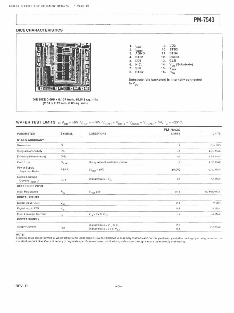
PM-7543DICE CHARACTERISTICS
1. loun2. loUT23. AGND4. STB15. LD16. N.C.7. SAI8. STB2
9. LD210. STB311. STB412. DGND13. CLA
14. Voo (Substrate)15. VREF16. RFB
Substrate (die backside) is internally connected10 VDO'
DIE SIZE 0.099 x 0.107 inch, 10,543 sq. mils(2.51 x 2.72 mm, 6.83 sq. mm)
WAFER TEST LIMITS at VDD= +5V; VREF= +1aV; Your' = VOUT2= VAGND= VDGND= av, TA= +25°C.
PM-7543GLIMITSPARAMETER SYMBOL CONDITIONS UNITS
STATIC ACCURACY
Resolution N
INL
12 Bi:s MIN_uuu_..--
Integral Nonlinearity
Differential Nonlineari!)'
LSB MAX
LSB MAX
:t1
DNL :1:1
Gain Error GFSE Using internal feedback resistor :t2 LSB MAX
Power SupplyRejection Ratio
Output Leakage
Current (Ioun>
PSAAAVOO=:t5% :to.002 %1% MAX
ILKG Digital Inputs ~ VIL :1:1 nA MAX
REFERENCE INPUT................--
Input Resistance RIN VREF pad 7/15 k!l MINIMAX
DiGITAL INPUTS
Digital Input HIGH
Digital Input lOW
VIH
VIL
2.4
0.8
VMIN
VMAX..........---..
Input Leakage Current IlL VINKOVtoVoO :ti fLAMAX
POWER SUPPLY---
Supply Current '00Digital Inputs K V'H or V'l
Digital Inputs =OV or V DO
2.00.1
mA MAX
...--NOTE:
Electrical tests <Ireperformed at wafer probe to the limits shown. Due to variations in assembly methods and normal yield loss, yield after packaging is nol guaranteed lorstandard product dice. Consult factory to negotiate specifications based on dice lot qualifications through sample lot assembly and testing.
REV.D -5-

ANALOGDEVICES fAX-ON-DEMAND HOTLINE
PM-7543
.. Page 19
TYPICAL PERFORMANCE CHARACTERISTICS
MULTIPLYINGMODEFREQUENCYRESPONSE
vs DIGITALCODE
MULTIPLYING MODETOTAL HARMONIC
DISTORTION vs FREQUENCYALLalTsONr-(MSa) anI:: SI.P B.
~~ a.P.. 81
~S B."0 8.
~; a.0... a.~ 82::. a,- (LSB) ao
100 'Ok lOOk
FREQUENCY (Hz)
Ik
SUPPLYCURRENTvsLOGICINPUTVOLTAGE
2
c!.8
00 2 3
VI" (VOLTS)
-70 0.032
VIII .6VRNSOUTPUT oP AMP: OP-42
-75 0.018
36 iD~
-. ..-< 48 ~!i
6Offi72 ~
-&0 ""'" . "'--'n .. "".0.010l§!...
0.0056
iD~§!
-&5 ..,. .....
84 -90 ..., 0.0032
..- . . <96
1M108
10M0.0018
lOOk-95
10 100 Ik tOk
FREQUENCY (Hz'
LINEARITYERROR vsDIGITAL CODE
0.5 ., ! I , , ,0.4-l'..+ t-+.~ +_.- !
i . , , i , j
0.3_~ Itt--t-i-,..1& 0.2 _.!. ..+ L~
~ ~ 1_ -+1_..+...+...' ; , 'a:: ..!Ii a ! .~~ -0.1
~::; -41.2
-0.3
LINEARITYERRORvsREFERENCEVOLTAGE
0.25
0.5 , --+..-..-..
-0.4
10
iDJJ>:!.
g0
-41.250-....
-0.5
6 -41.5-
a 512 t024 1536 2048 2560 3072 3684 .095
DIGITAL INPUT CODE (DECIMAL)
2 6
VRE,(VOLTS,
8
DNLERROR vsREFERENCE VOLTAGE
3 7 9 11
VOD (VOLTS'
0.5
0.25
iDJJ>:!....zc
-41.5
4 6
YRE' (YOLTS)
8 10
-6- REV.D
ANALOGDEVICESfAX-ON-DEMANDHOTLINE - Page 20
PM-7543SPECIFICATION DEFINITIONSRESOLUTIONThe resolutionof a DACis the number of states (2n) that the full-scale range (FSR) is divided (or resolved) into, where "n" isequal to the number of bits.
SETTLING TIMETime required for the analog output of the DAC to settle to within1/2 LSB of its final value for a given digital input stimulus; i.e.zero to full scale.
GAIN
Ratio of the DAC's external operational amplifier output voltage
to the VREFinput voltage when all digital inputs are HIGH.
FEEDTHROUGH ERROR
Error caused by capacitive coupling from VREF to output.Feedthrough error limits are specified with all switches OFF.
OUTPUT CAPACITANCE
Capacitancefrom lOUT' to ground.OUTPUT LEAKAGE CURRENT
Current appearing at loun when all digital inputs are LOW, or atIOUT2terminal when all inputs are HIGH.
GENERAL CIRCUIT INFORMATION
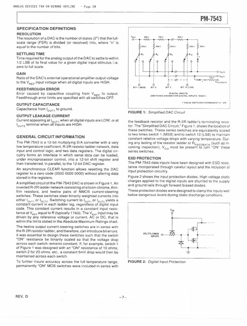
The PM-7543 is a 12-bit multiplying D/A converter with a verylow temperature coefficient, R-2R resistor ladder network,datainput and control logic, and two data registers. The digital cir-cuitry forms an interface in which serial data can be loaded,under microprocessor control, into a 12-bit shift register andthen transferred, in parallel, to the 12-bit DAC register.An asynchronous CLEAR function allows resetting the DACregister to a zero code (0000 0000 0000) without altering datastored in the registers.
A simplified circuit of the PM-7543 DAC is shown in Figure 1.Aninverted R-2R ladder network consisting of silicon-chrome, thin-film resistors, and twelve pairs of NMOS current-steeringswitches. These switches steer binarily weighted currents intoeither loun or IOUT2'Switching current to IOUT1or IOUT2yields aconstant current in each ladder leg, regardless of digital inputcode. This constant current results in a constant input resis-tance at V AEF equal to R (typically 11kQ). The VREF input may bedriven by any reference voltage or current, AC or DC, that iswithin the limits stated in the Absolute Maximum Ratings chart.
The twelve output current-steering switches are in series withthe R-2R resistor ladder, and therefore, can introduce bit errors.It was essential to design these switches such that the switch"ON" resistance be binarily scaled so that the voltage dropacross each switch remains constant. If, for example, switch 1of Figure 1 was designed with an "ON" resistance of 10 ohms,switch 2 for 20 ohms, etc., a constant 5mV drop would then bemaintained across each switch.
To further insure accuracy across the full temperature range,permanently "ON" MaS switches were included in series with
REV. D
10kl1
20kJJ 20kll 20kl1
5,.
,I,6
BIT 1 IMSBI
,II
6BIT 2
IIIIIIiI, r--,
~-" ~6 6
BIT3 BIT 12 IlSBJ
RHlDBACK
lOUT>
IOU",1Okll
DIGITAL INPUTS
(SWITCHES SHOWN FOR DIGITAL INPUTS "HIGH")
.. THESESWITCHES PERMANENTLY ..ON
FIGURE 1: Simplified DAC Circuit
the feedback resistor and the R-2R ladder's terminating resIs-tor. The "Simplified DAC Circuit," Figure 1,shows the location ofthese switches. These series switches are equivalently scaledto two times switch 1 (MSB) and to switch 12 (LSB) to maintainconstant relative voltage drops with varying temperature. Dur-
ing any testing of the resistor ladder or RFEEDBACK (such as in-coming inspection), VDD must be present to turn "ON" theseseries switches.
ESO PROTECTION
The PM-7543 data inputs have been designed with ESD resis-tance incorporated through careful layout and the inclusion ofinput protection circuitry.
Figure 2 shows the input protection diodes. High voltage staticcharges applied to the digital inputs are shunted to the supplyand ground rails through forward biased diodes.
These protection diodes were designed to clamp the inputs wellbelow dangerous levels during static discharge conditions.
Von
DTliTTl,CMOSINPUTS
-=
FIGURE 2: Digital Input Protection
-7-
v." ,oon won
20... 200J!
5, 5.

ANALOG DEVICES fAX-ON-DEMAND HOTLINE - Page 21
PM-7543
I FI,..OBACK
A _. 10kH
v""'om 2
10"T1
t'R"- R-\Ok"
t
FIGURE 3: PM-7543 Equivalent Circuit (All Inputs LOW)
AFEEDSACk
'""- R.,0kHR" 10'H
VREF
'OUT>
'OUT 1
t
t
FIGURE4: PM- 7543 Equivalent Circuit (All Digital Inputs HIGH)
EQUIVALENTCIRCUITANALVSISFigures 3 and 4 show equivalent circuits for the PM-7543's inter-nal DAC with all bits LOW and HIGH, respectively. The refer-ence current is switched to IOUT2when all data bits are LOW,and to lOUT' when aU bits are HIGH. The ILEAKAGEcurrentsource is the combination of surface and junction leakages tothe substrate. The 1/4096 current source represents the con-stant 1-bit current drain through the ladder's terminating resis-tor.
Output capacitance is dependent upon the digital input code.This is because the gate capacitance of MOS transistors in-creases with applied gate voltage. This output capacitance var-ies between the low and high values.
DYNAMIC PERFORMANCE
OUTPUT IMPEDANCE
The output resistance, as in the case of the output capacitance,varies with the digital input code. This resistance, looking backinto the 'OUT1terminal, may be between 11kn (the feedbackresistor alone when all digital inputs are LOW) and 7.5kQ (thefeedback resistor in parallel with approximately 30kQ of the R-2R ladder network resistance when any single bit logic is HIGH).Static accuracy and dynamic performance will be affected bythese variations.
The gain and phase stability of the output amplifier, board lay-out, and power supply decoupling will all affect the dynamicperformance of the PM-7543. The use of a small compensationcapacitor may be required when high-speed operational ampli-fiers are used. It may be connected across the amplifiers feed-back resistor to provide the necessary phase compensation tocritically damp the output.
The considerations when using high-speed amplifiers are:
1. Phase compensation (see Figures 7 and 8).
2. Power supply decoupling at the device socket and use ofproper grounding techniques.
APPLICATIONS INFORMATION
APPLICATIONTIPSIn most applications, linearity depends upon the potential ofIOUT1''OUT2'and AGND (pins 1,2, and 3) being exactly equal toeach other. In most applications,the DACis connected to anexternal op amp with its noninverting input tied to ground (seeFigures 7 and 8). The amplifier selected should have a low inputbias current and low drift over temperature. The amplifier's inputoffset voltage should be nulled to less than :t200~V (less than10% of 1 LSB).
The operational amplifier's non inverting input should have aminimum resistance connection to ground; the usual bias cur-rent compensation resistor should not be used. This resistor cancause a variable offset voltage appearing as a varying outputerror. Allgrounded pins should tie to a single common ground
point, avoiding ground loops. The VOD power supply shouldhave a low noise level with no transients greater than +17V.
It is recommended that the digital inputs be taken to ground or
VDOvia a high value (1Mn) resistor; this will prevent the accu-mulation of static charge if the PC card is disconnected from thesystem.
Peak supply current flows as the digital inputs pass through thetransition region (see the Supply Current vs logic Input Voltage
graph under the Typical Performance Characteristics). Thesupply current decreases as the input voltage approaches the
supply rails (Voo or DGND), i.e. rapidly slewing logic signals thatsettle very near the supply rails will minimize supply current.
OUTPUT AMPLIFIER CONSIDERATIONS
When using high speed op amps, a small feedback capacitor(typically 5-30pF) should be used across the amplifier to mini-mize overshoot and ringing, For low speed or static applications,AC specifications of the amp1ifier are not very critical. In high-speed applications, slew rate, settling time, open-loop gain, andgain/phase margin specifications of the amplifier should be se-lected for the desired performance. It has already been notedthat an offset can be caused by including the usual bias currentcompensation resistor in the amplifier's non inverting input ter-minal. This resistor should not be used. Instead, the amplifiershould have a bias current which is low over the temperaturerange of interest.
-8- REV. 0

ANALOG DEVICES fAX-ON-DEMAND HOTLINE - Page 22
PM-7543
=i~~SRI I
BIT1 X, _.~' X=:
:XH'. "I - -
'STRO os><os<- ....(STB1ST,
BEIHPUT I I--~ 10"" to '0
I
. 2, STB4) 1'1"1 ..3. 0..0f2
v~~-~-
fA rIf'
R AHC
2R 2R
FIGURE5: Simplified Circuit
Static accuracy is affected by the variation in the DAC's outputresistance. This variation is best illustrated by using the circuitof Figure 5 and the equation:
VERROR= Vas (1 + r;:~)where Ro is a function of the digital code, and:
Ao = 1Oka for more than four bits of logic 1,Ro = 30kn for any single bitof logic 1.
Therefore, the offset gain varies as follows:
at code 0011 1111 1111,
VERROR, =Vas (1 +!Qk!~ )=2 Vas1okQ
at code 0100 0000 0000,
(10ka
)VERR0R2 =Voo 1 + --- =4/3 Voo30kn
The error difference is 2/3 Vos'
Since one LSB has a weight (forVREF= +1OV)of 2.4mV for the PM-7543. itis clearly important that Vas be minimized, either using theamplifier's nullingpins, an external nullingnetwork, or byselection of
..
an amplifier with inherently fow Vos' Amplifiers with sufficientlylow Vos include PMl's OP- 77, OP-97. OP-O7, OP-27 and OP-42-
INTERFACE LOGIC OPERATIONThe microprocessor interface of the PM-7543 has been de-signed with multiple STROBE and LOAD inputs to maximizeinterfacing options, Control signals decoding may be done on-chip or with the use of external decoding circuitry (see Fig-ure 11).
Serial data can be clocked into the input register with STB 1.STB2, or STB4. The strobe inputs are active on the rising edge.STB3 may be used with a falling edge to clock-in data.
Holding any STROBE input at its selected state (i.e. STB1.STB2orSTB4at logicHIGHor S"f'B3 at logicLOW) will act toprevent any further data input.
When a new data word has been entered into the input register,
it is transferred to the DAC register by asserting both LOADinputs.
The CLA input allows asynchronous resetting of the DAC regis-ter to 0000 0000 0000. Th is reset does not affect data held in the
input registers. While in unipolar mode, a CLEAR will result inthe analog output going to OV.ln bipolar mode, the output will go
to -V REF'
INTERFACE INPUT DESCRIPTIONSTB1 (Pin 4), STB2 (Pin 8), STB4 (Pin 11) - Input RegisterStrobe. Inputs Active on Rising Edge. Selected to load serialdata into input register. See Table 1 for details.
STB3 (Pin 10) -Input Register Strobe Input. Active on Fail-ing Edge. Selected to load serial data into input register SeeTable 1 for details.
LD1 (Pin 5), LD2 (Pin 9) - Load DAC Register Inputs. ActiveLow. Selected together to load contents of Input Register intoDAC register.
CLR (Pin 13) - Clear Input. Active Low. Asynchronous.When LOW, 12-bit DAC register is forced to a zero code (00000000 0000) regardless of other interface inputs,
lBIT 11 X 8~~~2 x=
tn.,t'Tltt.m1ST.' tin;1ST.' lfio;
1- trnli LOADSERIALDATAr ' INTOINPUTREGISTER~t
i:P1 AND LD2
NOTES;'STROBE WAVEFORM IS IItVERTED IFSTB3IS USED TO STROBE SERIAL DATABITS INTO REGISTER.
"DATA LOADED ,,"SB FIRST.
4 t... +--1':'0' rl::J
LOAD INPUT REGISTER'SDATAINTOCAe REGISTER
FIGURE 6: Timing Diagram
REV. 0 -9-
ANALOGDEVICES fAX-ON-DEnAND HOTLINE - Page 23
PM-7543
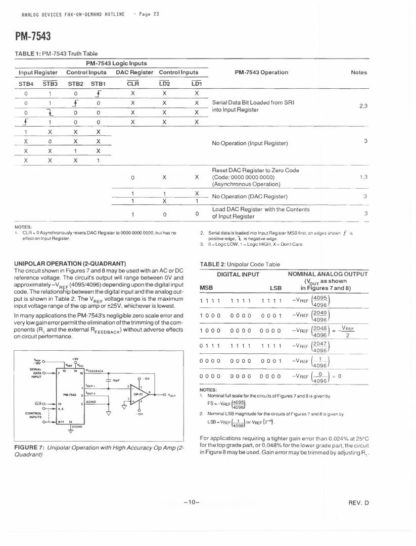
TABLE 1: PM-7543 Truth Table
PM-7543 logic Inputs
Input Register Control Inputs DAC Register Control Inputs PM-7543 Operation Notes
2.3
3
__nn___-
0 X 1,3
1
X
XReset DAC Register to Zero Code
(Code: 0000 0000 0000)
(Asynchronous Operation)
No Operation (DAC Register)
------------------
3
0 3
X1
----
0 Load DAC Register with the Contents
of Input Register -----NOTES:1- CLR~ 0 Asynchronouslyresets DACRegisterto000000000000,buthas no
ellee! on Input Register.
UNIPOLAR OPERATION (2-aUADRANT)The circuitshown in Figures 7 and 8 may be used with an AC or DC
reference voltage. The circuit'soutput willrange between QV and
approximately-VREF (4095/4096) depending upon the digitalinput
code. The relationship between the digital input and the analog out-
put is shown in Table 2. The V REF voltage range is the maximum
input voltage range of the op amp or :t25V. whichever is lowest.
In many applications the PM- 7543's negligible zero scale error and
very low gain error permit the elimination of the trimming of the com-
ponents (R1 and the external RFEEDBACK) without adverse effects
on circuit performance.
VA"-10V
SERIAlDATA
INPUT
-'-5V
CLR
Vour
ICONTROl. .
INPUTS:1
-ISV
=
FIGURE 7: Unipolar Operation with High Accuracy Op Amp (2-Quadrant)
2- Serial data is loaded into Input Register MS8 lI'st, on edges shown .f ISpositive edge. 1. is negative edge.
3- 0 = Logic LOW. 1= Logie HIGH, X= Don'tCare-
TABLE2:UnipolarCode Table
DIGITAL INPUT
MSB lSB
1 1 1 1 1 1 1 1 1 1 1 1
1000 0000 000 1
1000 0000 0000
01 1 1 1 1 1 1 1 1 1 1
0000 0000 000 1
0000 0000 0000
NOMINALANALOG OUTPUT
(VOUTas shownin Figures 7 and 8)
-VAEF (~~~~)
-v REF(204~")4096
-VREF(~~~~) = ~-vREF (201I
)4096---------
-vREF bo1-6)------
-v REF (40~6) = 0
NOTES:1. Nominalfullscale forthecircuits01Figures7 and 8 isgivenby
FS =-VREF{4095 }-4096
2. Nominal LSB magnitude for !he drcuits 01Figures 7 and 8 is given by
LSB =VREF(-1---)or VREF (2--<1) -4096
For applications requiring a tighter gain error than 0_024% at25"C
forthetop grade part,or 0.048% for the lower grade part, the circuit
in Figure 8 may be used. Gain error may be trimmed by adjusting R1 -
-10- REV.D
5TB4 5TB3 5TB2 STB1 CLR lD2 lD1
0 1 0 S X X X0 1 S 0 X X X Serial Data Bit Loaded from SRI--
1-intoInputRegister0 0 0 X X X
S 1 0 0 X X X---
1 X X X_____n__"
X 0 X XNo Operation (Input Register)
X X 1 XX X X
ANALOGDEVICES fAX-ON-DEMAND HOTLINE - Page c~
PM-7543
6VOUT
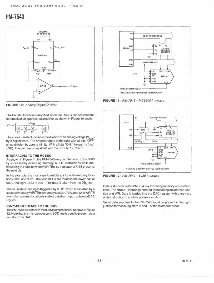
FIGURE 10: Analog/Digital Divider
The transfer function is modified when the DAC is connected in the
feedback of an operational amplifier as shown in Figure 10 and is:
Vo = (5~-~:~~H ~)The above transfer function is the division of an analog voltage (VREF)by a digital word. The amplifier goes to the rails with all bits "OFF"since division by zero is infinity. With all bits "ON," the gain is 1 (:t1LSB). The gain becomes 4096 with the LSB, bit 12, "ON."
INTERFACING TO THE MC6800
As shown in Figure 11, the PM- 7543 may be interfaced to the 6800by successively executing memory WRITE instructions while ma.nipulatingthe data between WRITEs, so that each WRITE presentsthe next bit.
In this example, the most significant bits are found in memory loca-tions 0000 and 0001. The four MSBs are found in the lower half of
0000, the eight LSBs in 0001. The data is taken from the DB? line.
The serial data loading is triggered by STB1 which is asserted by adecoded memory WRITE to a me.morylocation, ANI. and $2. A WRITEto another address location transfers data from input register to DACregister.
PM.7543 INTERFACE TO THE 8085
The PM-7543'sinterfacetothe8085 microprocessor is shown inFigure12. Note that the microprocessor's SOD line is used to present dataserially to the DAC.
AO16-61T ADDRESS BUS
At.
RMM~
u2
Deo
DBT
.5V
FROM SYSTEM RESET
.ANALOG CIRCUITRY OMITTED FOR SIMPLICITY
FIGURE11: PM-7543 - MC6BOO Interface
.ANALOG CIRCUITRY OMITTED FOR SlIolPUClTV
FIGURE 12: PM- 7543 - 80B5 Interface
Data is strobed into the PM- 7543 by executing memory write instruc-tions. The strobe 2 input is generated by decoding an address loca-tion and WR. Data is loaded into the DAC register with a memorywrite instruction to another address location.
Serial data supplied to the PM- 7543 must be present in the right-justified format in registers Hand L ofthe microprocessor.
-11- REV.D
VIMo----J!.IRFB VDD +SV
PM.7543
11 115loun VR£F
(9) ADDRESSBUS 116>--' Ao-1O
8095
ALE
WR+W
(9)AD0-1 DATA
r-SOD

r-r--
1001 Audio
1002 Audio sumer Audio/SpeakerPhon X
1003 Audio Alldio X
1043 .. Audio iSpeech X
1044 Automotive High-Side Current Sense X
1045 omotive T elematics System #
1004 mmunications(Wired) CableModem X
1005 mun X
1006 mmun (Wired) X
1007 .iCommun x #
1008 Communi ""'""""'"'Y X"
1009 iCommunicati SL X
104211 Communications C"""" I;,..,nn"rI""m X1046 !r.nmmlln verIP X
1010 '(Wireless) tion X
1011 less) t/SoftCell X
1012 ireless) s) X
1047 reless) PDA #
1013 Drive X
1014 , rd X
1015 'Imaginideo r X1016 Ima,i!:1gNid, ICamera #
1017 ImagingNideo X
1018 ImagingNideo ax X1019 ImagingNideo !Video Capture Board #
1020 Industrial Flow MeterinQ X
1021 ial Machine Vision X
1022 ial Measurement/Process Contro #
1023 I Motor Control X
1024 ial VibrationAnalysis X
1025 ial !Weigh Scale X
1026 ATE Equipment X
1027 ntation
igCqUisition
X1028 uL;U/Je X1029 Instrumentation ' L Ie System Tester X
1030 i InstrumentationQ", ..".... X
1031 1 Instrumentation #
1032 I! Medical r X
1033 Medical #'-",
1034 Medical callmaging/Ultrasound X
1035 Medical or X
1048 Medical X? ..........
1036 Militar /Aerospace s X1037 orking FA #1038 orking r Cross-Connect X1039 orkin #1040 Solution X1041 king r EDFA (High-Power) X1049 Optical Networking T OC!t Equipment X
INOTE: 11ST ten live; 21-30 end of July/1st of August; all 49 needed for Matrix 3.0 release end of June 03

ANALOGDEVICES fAX-ON-DEMAND HOTLINE - Page 25
PM-7543
R,
Vo.,-10V
SERI"LDAn
'"POT
VOUT
cu. 3,AGNO
CONTROL
INPUTS
-=-
FIGURE 8: Unipolar Operation with Fast Op Amp and GainErrorTrimming(2-Quadrant)
The DACregistermustfirstbe loaded withall is. R1is then adjusteduntil VOUT=-V REF(4095/4096). Inthe case of an adjustable VREF'R1and RFEEOBACKmay be omitted, with VREFadjusted to yield thedesired full-scale output.
BIPOLAR OPERATION (4-aUADRANT)Figure 9 details a suggested circuitfor bipolar, or offset binary opera-tion. Table 3 shows the digital input to analog output relationship,The circuit uses offset binary coding, Two's complement code canbe converted to offset binary by software inversion of the MSB or bythe addition of an external inverter to the MSB input.
Resistors R , R4' and Rs must be selected to match within 0.0' %and must air be of the same (preferably metal foil) type to assure
temperature coefficient match. Mismatching between AJ and A4causesoffset and full-scale errors while an A5 to A4 and R3 mismatch willresult in full-scale error.
Calibration is performed by loading the DAC register with ,00000000000and adjusting R1until VOUT=OV.R, and R2 may be omitted by
'SY R,
V,NIS
PM-7543Vo.,R,
100" COfjTROLBITS
8-11 '.~
FROMSYSTEMRESH
ISERIALDATAINPUT
CONTROLINPUTS
FIGURE 9: Bipolar Operation (4-Quadrant, Offset Binary)
REV. D
TABLE 3: Bipolar (Offset Binary) Code Table
DIGITAL INPUT NOMINALANALOG OUTPUT
LSB (VOUT8sshown in Figure 9)
, , 1, + VREF (~~:})0 0 0 , + VREF (~._ )2048
MSB
1 1 1 1 , , 1,, 000 0000
NOTES:
1. Nomina!full scale for thecircuitsof Figure9 isgiven by
FS ~ VRf,F1
2047 )2048
2. Nominal LSB magnitude tOf !he circuits of Figure 9 is given by
Lffi=VREF/~\.\20481
adjusting the ratio of RJ to A4 to yield VOUT= OV. Full scale can beadjusted by loading the DAC register with 111' 11" , 111 and ei-
ther adjusting the amplitude of VREForthe value of As until the desiredVOUTis achieved.
ANALOG/DIGITAL DIVISION
The transfer function for the PM-7543connected in the multiplyingmode as shown in Figures7 and 8 is:
VO=-VIN (;; + ;.~ +;~ + "';i~)
where Ax assumes avalueof 1 for an "ON" bit and Oforan "OFF" bit
R.20kQ R,
VOIlT
AH"LOGCOMMON
-12-
1 a 0 a 0000 0000 0
0 1 " l' 1 1 1 1 1 1-V REF (---1-)2048
0000 0000 000'-VREF (?_Q1?_)2048
0000 0000 000 a-V REF (}6::-)