devices(u c0oflcado ffaricrtion strte of univ xi … · designed the system, it was built ta our...
TRANSCRIPT

17 -ft$9 979 BERNE MISTED FfARICRTION OF XI-YVSI MNOLITHIC 1/1DEVICES(U C0OFlCADO STRTE UNIV FORT COLLINS
UZXC~ffiSlF 0 ROBI SO 19 SEP 67 F49620-96-K-0021 FO91 - M

L28ALI 13j
-- I M2
.1111125 11114 __
w w W lw W w Ww w w w w w

SECURITY CLASSIFICATION OF THIS PAGE
REPORT DOCUMENTATION PAGEls R b. RESTRICTIVE MARKINGIL i
2a. ECU~rf E=ff11WR CTROIY3. 'DISTRIBUTION /AVAILABILITY OF REPORT________________________________________ Approved for public release,
,2b. DECLASSIFICATION IDOWNGRADING SCHEDULE distribut ion Unlimited
tMING ORGANIZATION REPORT NUMBER(S) 5. MONITORING ORGANIZATION REPORT NUMBER(S)
__ __ __ __ _ __ __ AFOSRt.T7. 8 7 -18 i .*OF PERFORMING ORGANIZATION 6b. OFFICE SYMBOL 7a. NAME OF MONITORING ORGANIZATION
a) (If appicabl)
Q i~atin1.q 11nivprq tjAFOSR/NEESS (C S Stae, and ZIP Code) 7b. ADDRESS (City, State, and ZIP Code)
Fort Collins, CO 80523 Bldg 410__________________ __________ Bolline AFB, DC 20332-6448
SE OF FUNDING/ SPONSORING 1 b. OFFICE SYMBOL 9. PROCUREMENT INSTRUMENT IDENTIFICATION NUMBER
WIATO I NE F49620-86-K-0021O ESS (City. Staft, a&W ZIP Codle) 10. SOURCE OF FUNDING NUMBERS
PROGRAM PROJECT TASK WORK UNITBldg 410 ELEMENT NO. NO. S58 NO 00CCESSION NO.
Bolling AFB, DC 20332-6448 61102F DARPA11. TITLE (hickWd Securfty Classfication)
Beam Assisted Fabrication of III-V/Si Monolithic Devices
12. PERSONAL AUTHOR(S)Prnf Rdghirmtnm
13a. TYPE OF REPORT 13b. TIME COVERED 114. DATE OF REPORT (YosriMorithDey) 15.PG ON
Arnnim 1 FROM9NvL6TO 1190c87116. SUPPLEMENTARY NOTATION L %,
ELECTE17. COSATI CODES 18. SUBJECT TERMS (Coatlnue on reverse if noc ~ IvfYI~~
FIELD GROUP SUB-GROUP jL(&
19. AMWCT (Continu on reverse if necessary and identify by block number):The objective of this research project is to-xlr two new methods fordeposition of Ill-V semiconducting films on'S V substrates. Using gas-sourcemolecular beam epitaxy (KBE) and photon-beam and electron-beam assistedmetal-organic chemical vapor deposition (MOCVD),,GaAs-nd other Ill-V filmswith abrupt heterojunctions are being formed epitaxially on Si, and by meansof optical and electrical characterization the suitability of the resultingIll-V/Si structures are being examined for use in Monolithic devices.
UNCLASSIFIED/UNLIMITED 0 SAME AS RPT 0 TIC USERS22a. NAME OF RESPONSIBLE INDIVIDUAL 22b TELEPHONE (Includte Area Code) 22c. OFFICE SYMBOL
MaloI 77)743 1 NIo00 form 1473. JUN 36 Previous vdition or* obsolete. SECURITY CLASSIFICATION OF THIS PAGE

PWOSRTR-
Annual PP-port
First Year(9/1-1/86 - 9/10/87)
"Beam Assisted Fabrication ofIIl-V/Si Monolithic Devices"I
-AM@Cotract #F49620-86-K-0021
Colorado State University OIFort Collins, CO) 80523 COSPY~
6
ion For
PI: Gary Y. Roinson.40inced 5
Co) P1's: George J. Collins LcationRaj Solanici (Oregon, Graduate Center)
Distribution/__
Availability Codes
jAvail -and/or*Dtst Special
x4
All,
2
AMml 1ort(Covering 9/1.1/86 - 9/10/87)
"Beam Assisted Fabrication of III-V/Si Molithic Devices"
The objective of this research project is to explore two new methods
for deposition of III-V si i n films on Si substrates. Using gas-
source molecular beam epitaxy (MBE) and photon-beam and electron-beam
assisted metal-organic chemical vapor deposition (IVCVD), GaAs and other
III-V films with abrupt heterojunctions are being formed epitaxially on Si,
and by means of optical and electrical characterization the suitability of
the resulting III-V/Si structures are being examined for use in monolithic
devices.
Gas-Source MEE (Gary Y. Robinson, Colorad State University)
Gas-source M combines thermal cracking of the gaseous hydrides AsH3
and PH3 to produce molecular beams of As2 and P2 , respectively, with
conventional MBE technology for Group-III molecular beam production frn
effusion cells. The availability of both As 2 and P2 beams allows
incorporation of buffer layers of wide composition range and lattice
parameters and for exploration of III-V materials grown by MBE on Si other
than GaAs.
The major accomplishments of the first year consisted mainly of
design, procurement, installation, and check-aut of the custom equipment
needed for gas-scurce MM. The major equipment items were (refer to Figures
1 and 2):
I Gas delivery svs t for the hydrides with provision for precisecontrol and rapid switching of PH and AsH flow rates. Wedesigned the system, it was built ta our specifications by a
ommercial vendor, installed, and checked out in our laboratory.

wvpwm~Nmw~tWag %wr
3
V- a
-J -
z1 0. I-Z
0 E 40 Utax :IR U)a
w 3: . 4 2AO x
~ ~ - 1 ~ Li.- 0 0 0 0
C~~Us 0) 9CL
00 aW4
-Fi dalE
UJ 0
cog 0, I04 o 2'2 -a
.0 -
0 0 0 IDIJC
0, 00 , U
CL 2
* 4L~ C0
IL
060
0
1%
CC0II
G0 0

4
Volvo Control
ExhustPressure Controller
,..i u -- 4200 -2000 Tarr
30-5 psiTransducer
N 1 System Leok 1- -10-4 Tarr
100%"Dump"s
I Vented SteelAir Sr ,,,OGas CabinetInlet 4Pup 1 200 -1000 elm
~~41
Scrubber
FIGURE 2 SCHEMATIC DIAGRAM
HYDRIDE DELIVERY SYSTEM

e Gas-crackina oven for reducing the hydrides PH and AsH3 tomolecular beams of P and As After design by us, cracking ovenwas built in Japan a&d deli ved late in the year.
* Pum~ina system to accomodate the large H gas load and for saferwval of the toxic hydrides. The system csists of a He closed-cycle cry paup, mechanical pump, and gas scrubber.
e Other recialized .aimrv needed for growth and characterizationof films on Si substrates. These included:
- Glove box for ME introduction chamber for preparationof Si wafers in axygen free atmosphere,
- New substrate heater for cleaning Si at temperatures ashigh as 1200C, and,
- A double-crystal X-ray diffzract te for structuraldaracterization of III-V films an Si.
All of the above equipment is now in place and is being integrated into one
system with a single computer for control of the ME growth process.
Wile the above equipment was being put into place to provide gas-
source MBE capability, epitaxial growth using conventional MBE was
urdertacn. During the first year we have grown:
• GaAs n S to establish the proper Si substrate cleaning techniquesand growth procedures in our laboratory,
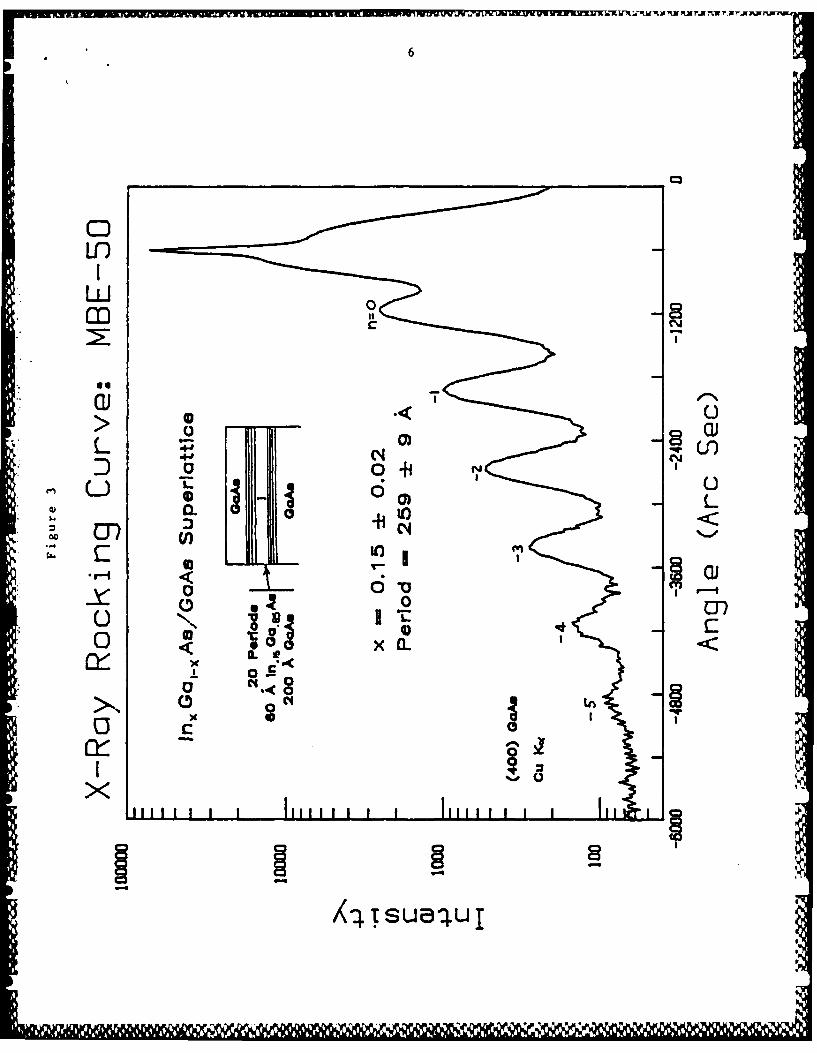
e InGaAs/GaAs suerlattices on GaAs. We intend to use superlatticesof InaAs/GaAs as a buffer layer to pin misfit dislocations whengrowing GaAs and other III-V layers on Si. X-ray diffractionspectra (see Fig. 3) indicate sharp heterojunction interfaces andexcellent coherency of the periodic structure.
e GaAs on GaAs to qualify our new MBE system. Characterizationincluded Hall-van der Pauw, C-V profiling, photoluminescence, SIMS,AES, and X-ray diffraction.
Efforts for the second year will exploit the specialized equipment
installed and made operational during the first year by growing InP on Si
using gas-source MBE. Buffer layers of GaAs and InraP will be examined as
well as direct grown on Si.
CC
0~
> C)L un!
C14~
0 41u 6o L
00 M
002c 0
C) v
00
oC4 00 0<C0
0 0xC
[tl II/4TSUaqRjI
111 iii li

7
Enerav Assisted Deposition of GaAs on Si (G. J. Collins, Colorado State
University)
The progress of the growth of GaAs on Si with an energy assisted
technique has been in the development of the deposition technique,
realization of the reactor and support system design, and the completion of
a proposal for further funding. The developnt of the deposition technique
and the completion of the proposal has directed cur research. The reactor
design is a consequence of that effort. The laser assisted technique
originally proposed has the advantage for both direct writing and low
temperature deposition. However, the working with the laser can be
problematic as well as the high cost may be prohibitive for the camnercial
development. As a result we have pursued the development of the electron
beam for energy assisted deposition techniques. The realization of such an
energy source has paralleled the GaAs on Si research. Organometallic
feedstock gases have been decomposed and AIN film deposited and results
presented in the attached preprint (Appendix A). This deposition technique
is very relevant and is being applied to our GaAs on Si research since it
possesses many advantages in both the gas phase decxmposition of the gases
as well as the ccuposition of the deposited films.
The proposal has just been completed and represents our efforts to
elucidate the physical problems associated with the III-V deposition on Si
and cur proposed solutions. Funding will be sought as the proposal is being
sent out in the middle of October.

8
Laser Indue Epita"xv of II-V Omv=unds (Raj Solanki, Subitract to
Graduate Center, Starting Date: December 1, 1986).
During the first year, most of our efforts were directed towards the
construction of the laser deposition system. Although most of the
cmmtruction was cmpleted at the end of the second quarter, additional
modifications were incorporated during the third quarter. At this time
initial depositions were also achieved.
The process of laser-induced heteroepitaxy of III-V campoudrs is new
and not well dharacterized, therefore we started with a simple system, i.e.
growth of GaP on Si since they have a close lattice match. In order to
systeatically approach this issue, we spent the last quarter by first
characterizing the homoepitaxy of GaP. This phase of our investigation
provided us with a wealth of information on the laser process. Some of
these results are summarized in the attached preprint (Apperdix B). The
eapirical results obtained are used to help us develop a model of this
groth process.
Over the past mnth, we have been investigating heteroepitaxy of GaP
on Si. The deposition ccnditions here are significantly different than frm
hcmrepitaxy, h%&ve, we are making good progress. We expect to continue
working on the heteroepitaxy of GaP on Si for the next few months before
moving on to heteroepitaxy of other II-V campounds on Si.

1* 9
Appendix A
LASER ENHANCED CVD OF ALUMINUM NITRIDE ON INDIUM PHOSPHIDE SUBSTRATES
T.Y. SHENG, L.R. THOMPSON, T. HWANG AND G.J. COLLINS
DEPARTMENT OF ELECTRICAL ENGINEERING
COLORADO STATE UNIVERSITY
FORT COLLINS, CO 80523
ABSTRACT
The chemical and electrical properties of laser CVD aluminum nitride
deposited on n-InP substrates have been investigated. XPS and AES have beer.
used to analyze the AIN-InP interface and the bulk chemical composition.
FTIR was used to characterize water and OH bond content. The aluminum to
nitrogen ratio of the laser deposited film is approximately 1, comparable to
a conventional thermal MOCVD AIN film. Photoluminescence (PL) has been
found to provide a convenient probe of surface sensitive properties of InP
following wet chemical cleaning and AIN film deposition. The acidic
solution clean of the n-InP wafers prior to film deposition gives rise to
high PL intensity, whereas a basic solution gives rise to a low PL signal.
PL measurements were correlated with the observed C-1. characteristics of
laser deposited AIN/InP MIS structures. A strong inversion layer can be
formed in the n-InP substrate. The surface state density distribution has a
minimum about 3x10" eQlcrr2 located 0.4 eV below the conduction band.
Frequency dispersion of the AIN/InP MIS structures biased into accumulation
is attributed to the bulk insulator while the frequency dispersion in the
-'1 S\/-
/ 10
depletion region is caused by the surface states at the insulator-
semiconductor interface.
I. INTRODUCTION
Herein, we report low temperature laser CVD of AIN, outline deposition
conditions, a.id present both chemical and electrical characteristics of
laser deposited AIN/InP MIS structures. The interfacial characteristics of
insulator/semiconductor structures on Ill-V compounds have been studied
extensively in recent years( ). One dielectric type contains native oxides
grown by using thermal or anodic techniques while a second type is a
deposited insulator. One advantage of the native oxide growth is that
surface contamination problems can be minimized since the process of
oxidation results in the formation of a subsurface interface. However, the
native II!-V oxides are not satisfactory insulators primarily because the
band gap of the III-V native oxides is smaller than that required for an
acceptable dielectric insulator. With the deposited insulator, process
induced surface damage to the Ill-V substrate often occurs giving rise to a
large interface trap density. Moreover, conventional high temperature
deposition processes are not suitable for Ill-V compound semiconductors due
to incongruent thermal decomposition.
Aluminum nitride films are used in microelectronics, optical, and
integrated optic applications( ) as a non-absorbing, non-dispersive high
refractive index material( >. It has chemical, physical and electrical

( properties suitable for these applications. The large bandgap of aluminum
nitride (6 eV) makes it a very good insulator( ). Its low diffusion
coefficients for impurities makes it a canidate passivating layer for
semiconductor devices. Unlike most Al containing III-V compounds, aluminum
nitride is stable in air as well as in vacuum to high temperature( ).
Aluminum nitride also allows reduction of interface trap densities in InP
MIS structures, provided there is an absence of oxygen during film
deposition; hence, reduce native oxide growthoccurs at the interface.
Finally, aluminum nitride is a III-V material,-therefore, it is electrically
inactive in a III-V compound semiconductor substrate such as InP and GaAs
( ). In other words, AIN-InP or AIN-GaAs interdiffusion, if there is any,
is not expected to induce major detrimental effects.
Common to previously reported MIS structures on III-V substrates are
two major problemJ: an undesired curreny drift and interfacial
instabilities. The instabilities have been shown to depend on surface
preparation and surface damage induced during insulator deposition. Our
results presented herein suggest that laser assisted CVD may provide less
radiation damage to the substrate surface as vell as the use of a lower
deposition temperature. This conclusion is supported by the measured
properties of MIS structures given in part IV.
II. EXPERIMENT
A large number of process steps are involved in the fabrication of a
simple metal-insulator-semiconductor(MIS) structure on InP and MIS
electrical properties are effected by all combined process steps. In order
"Al

12
to better isolate the effects of each processing step.,. photoluminescence(PL)
measurements can be used prior to and after each step of the MIS fabrication
process( ), to monitor the changing electronic properties of the InP
surface and acts as a guide to help determine the optimum processing
sequence for making MIS diodes or MISFETs as shown below.
The n-InP substrates were first chemomechanically polished in a I.
bromine methanol solution. The wafers were then subjected to various
chemical etches and PL measurements were carried out in air following each
chemical cleaning sequence. InP samples were e-tched in the following active
chemicals: (1) A single step etch in 4H SO : IH 0 : IH 0; (2) A three
steps etch including NRL ( IHF : IHCI : 4H 0 ), 12 ml NRL with 1 drop H 0
and HCI(10.) and HF(1%); (3) A one step H 0 aqueous solution. Comparisons
between the etches used were quantified by the observed PL data.
The experimental setup for the PL measurements is shown in Fig. 1. The
front InP surface was illuminated with an He-Ne laser( = 633 nm) at a power
density of I W/cm . An optical filter removes background light other than
the 633nm radiation. The optical penetration depth for a 633nm photon
impinging on an InP wafer is of the order of 150nm( ). The integrated PL
signal is picked up from the back side of the InP sample and detected by a
silicon photodiode. The observed PL intensity was distinct to each etch and
correlated with C-V data as described in section IV.
A schematic diagram of the laser CVD system and typical deposition
conditions are shown in Fig. 2 and Table I, respectively. The samples upon
which AIN was to be deposited were first cleaned as described above, placed
into a vacuum chamber and turbomolecular pumped for 2 hours. The base

13
pressure as monitored by an ion gauge was in the mid;of 10 Torr. During
the pumping period, the samples were maintained at 150 C to assist
desorption of water vapor and other surface contaminations. A Lumonics
excimer laser operating on the 193nm ArF* transition was used to photo-
dissociate the feedstock reactant gases chosen for the AIN deposition. Our
* choiced feedstock gases were trimethylaluminum (TMA: AI(CH ) ) and ammonia
(NH ) to obtain Al and N atoms respectively. Both TMA and NH ahb!seo 193nm
radiation strongly and form free radicals( ). Dissociated free radicals
both react in the dissociation volume and condense on the substrate
underneath the beam-dissociation region to form a film. We make no attempt
in this work to unravel molecular gas phase kinetics nor competing surface
reactions.
The macroscopic LCVD deposition parameters affecting AIN film
. properties were found empirically to include: the laser power, TMA/NH flow
rate ratio, ambient background pressure of the CVD reactor and the choice of
substrate temperature. During AIN film deposition, the substrate
temperature was maintained at 30 C for the InP substrate, the highest
temperature we can sustain without causing incongruent decomposition( ).
Total reactor pressure was controlled by a downstream automatic butterfly
valve and a mechanical pump. TMA/NH flow rate ratios were fixed at a value
of 1:40 after prior empirical studies. The typical LCVD deposition rate is
about 150 A/min. The refractive index and thickness of the AIN have been
determined by an ellipsometer. Typical index value for the LCVD films are
1.70 to 2.0 (bulk value 2.18). It was noted that both the index and the
electrical resistivity increase as the substrate temperature employed

14
increases. Simply speaking, using laser CVD, we deposit aluminum nitride
films which have properties comparable to AIN films deposited by using
conventional thermal CVD. Note that thermal CVD requires substrate
temperatures greater than 800 C, which is not acceptable for InP substrates.
AIN film properties for both thermal and laser techniques are compared in
Table II. I
After AIN deposition, post-deposition annealing occurs at 325 C, in Ar
forming gas for 36 minutes. This anneal has been used to improve the
semiconductor-insulator interface properties. Next a front contact to the
MIS structure is formed by evaporating a pattern of circular aluminum dots
on the AIN film approximately 5x18 cm in area and 106A in thickness.
Indium soldering on the InP backside was used to make ohmic contact to the
n-InP substrate. The electrical properties of this MIS structure are giving
in section IV.
III. XPS, AES AND FTIR STUDIES OF LCVD AIN THIN FILMS
Large variations in the MIS structures electrical properties were
observed when the deposited insulator preparation procedure varied. This is
judged due to changes in the interface native oxide. The undesired native
oxide generates both fast interface states and provides bulk trapping sites.
Therefore, we studied the structure of the interface oxide layer via XPS and
AES in order to better understand the measured MIS electrical properties.
Atomic bonding and chemical composition of native oxide films grown on
InP as a consequence of different chemical treatments were comparaed by the
X-ray photoelectron spectroscopy (XPS) technique. XPS spectra were

15
obtained with a Perkin-Elmer Physical Electronics model 548 AES/ESCA system
using a Magnesium X-ray target source. The rastered sputter gun used for
XPS depth profiling operated at IKV, 18 uA/cm current densities over 7x7 mm
sample area. The XPS compositional profiles of InP wafer treated with 4H SO
IH 0 : IH 0 shows spectra that suggest the native oxide consists of
InPO , although a small P-oxide signal is present. That is, the peak
seperation between the P-InP and the P-oxide peak is approximately 4.5 eV,
which corresponds to the value observed for InPO ). The seperation
between the 0 IS and the P-oxide peak is 398.2-eV also indicating that this
P-oxide is bonded as InPO ( ). In addition, in curve fitting the In 3d
line at the surface, two peaks were used and a good fit was obtained by
holding the width of In-IrP (FWHM = 1.67 eV) peak constant. The seperation
of the two peaks is 1.3 eV, which is in accordance with prior InPO work(
). The XPS compositional profiles of an InP wafer cleaned with H 0 were
characterized by the thickness of the native oxide. It was much thicker for
a H 0 clean as confirmed by ellipsometric thickness measurements. Our XPS
data show that the composition of the native oxide with H 0 cleaning is
also InPO . Other compounds such like In 0 , P 0 may be present in the
InPO oxide layer, however, their presence is hard to quantitate due to the
weak XPS signal of the P-oxide. The 0 Is peak processes a 2.8 0.1 eV FWHM
which indicates that H 0 cleaning creates InP samples which have thicker as
well as multi-components oxides. Prior researchers( ) attribute to this
native oxide the observations of both current drift and C-V hysteresis.
Fig. 4 shows that the InP substrate etched by a H SO solution prior to AIN
deposition has less hysteresis than a substrate treated with a H 0 cleaning
-I . .

16
solution. Both the larger surface state density andobserved C-V hysteresis
of the sample with H 0 predeposition cleaning may be attributed to the
existance of thicker native oxides.
The bulk composition of deposited films on InP substrates were also
examined by Auger electron spectrascopy (AES). AES were obtained by using a
Perkin-Elmer Physical Electronics model 548 AES/ESCA double pass CMA Auger
spectrometer operating in dN/dE mode. Incident electron beam energy was
3 KeV with a typical beam current of 15 uA. Ion sputtering for depth
profiling was performed with a beam of Ar ionsr Reference samples of both
Al 0 and AIN were available. Anodically grown Al 0 was used as a
reference to identify the AI(KLL) and 0(KLL) peak amplitudes in the Al 0
matrix. A MOCVD AIN film was used as a reference sample to identify the
AI(KLL) and N(KLL) peak amplitudes in the AIN matrix. Relative atomic
sensitivity factors (ASFs) of the 0(KLL), AI(KLL) and N(KLL) characteristic
peaks, as estimated from both anodically grown Al 0 and MOCVD AIN reference
films, are 8.42, 0.055 and 8.25, respectively. The relative peak to peak
intensities of 0, Al and N spectra characteristic of LCVD AIN films were
then measured and compared to the standards in order to determine the AIN
film composition. The AES composition determination was verified by RBS
analysis done at Sandia Laboratories. Both techniques give a 1:1 atomic
ratio for AIN. The oxygen contamination varied from 5% when employing a
20 C substrate temperature to less than I for a 400 C substrate
temperature.
Fourier transform infrared (FTIR) absorbance spectra of LCVD AIN
samples were examined in the spectral range 440 cm to 488 cm . The main

17
absorption peaks observed in the FTIR spectrum are discussed below. Peaks
centered around 3450 cm and 1646 cm are related with impurity water bands
( ). These bands are significant for samples deposited at 200 C
substrate temperature but decrease dramatically for samples deposited with
increasing temperatures. The absorption band around 460 cm was observed
for films deposited with low temperature but diminished when deposition
temperature is higher than 300 C. This is consistent with the
identification of the absorption peak at 468 cm to a vibrational mode of
the Al 0 molecule( ). The spectrum shows peaks around 610 cm , 655 cm
and 670 cm , which corresponds to lattice TO phonons in AIN( ). These
three peaks exhibit increased intensity and sharpen in shape with
increasing deposition temperature. These results support the AES analysis
for oxygen contamination in LCVD deposited AIN films.
IV. MIS ELECTRICAL MEASUREMENTS AND CORRELATION WITH PL DATA
Table III lists the nomalized PL intensity of n-InP substrates( N =
1 18@ cm ) at each individual fabrication step of the MIS structure. The
PL intensity(arbitrary units) is around I for a InP surface cleaned by Br-
MeOH etchant. Generally speaking, the PL intensity increases after
immersing the InP sample into an aqueous acid solution and decreases after
immersing a similar samlpe into an aqueous H 0 solution, in agreement with
prior reports( ). Among all acids, the H SO solution results in the
largest PL signal. Surface roughness created by chemical etches has been
examined by optical scatterometer at the university of New Mexico
(Dr. JR. Mcneil) and we found no correlation to the PL intensity trend.

°"W WVW.V
Therefore, we can exclude the consideration of light~scattering by
chemically induced surface roughness.
Resistivity of the LCVD AIN films measured at a electric field strength
of 2 MV/cm, is determined by a steady state current versus time measurement
to be about 10 ohm-cm (AIN bulk value 18 ohm-cm). Breakdown field
strengths for LCVD AIN films are in the range from 2 to 4 MV/cm. The
leakage current and resistivity of LCVD films deposited at the same
substrate temperature are independent of predeposition surface cleanings.
However, the electrical properties of the AIN/LnP interface depend markedly
on the predeposition chemical surface cleaning. Figs. 3(a) and (b) show
high frequency (I MHz) C-V characteristics for two of the MIS structures
both deposited at 308 C on n-InP. One is cleaned with NRL solution prior
to AIN deposition and one is cleaned with H 0 . Note that a qualitative
correlation is observed between the observed PL intensity following the
substrate clean and the interface state density N as determined by MIS C-V
data. The sample with H SO solution cleaning has similar C-V characteristics
(shown in Fig. 4) to the sample with NRL cleaning. Both also have the same
PL intensity following surface cleaning. The sample subject to H 0
cleaning has a distinct C-V characteristic (large N ) which corresponds to
the smaller observed PL intensity.
A measured capacitance versus bias voltage curve measured at I MHz for
AIN films in the MIS structure is shown in Fig. 4. The InP substrate was
etched with a 4H SO : IH 0 : 1H 0 solution prior to the LCVD AIN
deposition. The measured hysteresis is small, even when the bias ramp
voltage was 10 volts. An accurate knowledge of the substrate doping
- a r . rr %

19
density is required for calculation of the ideal C-V;curve. Meiners( )
pointed out that the doping density of a wide band gap semiconductor(e.g.
InP, GaAs) as measured from the deep-depletion method is more accurate than
those obtained from Hall measurements. Using the deep-depletion method, we
measured the carrier density to be 2.3x10 cm . From th, measured
substrate doping density and measured value of dielectric capacitance
obtained from accumulation, a theoretical capacitance curve neglecting the
effect of surface states was calculated. This ideal C-V plot is given in
Fig. 4 as the dotted line. The agreement between the theoretical minimum
value of capacitance and the measured capacitance data suggests that the
InP surface under the AIN insulator can reach inversion, i.e. a p-channel
can be formed in the n-type InP substrate. Using the Terman method( ), an
analysis of the results shown in Fig. 5 indicates that a minimum surface
states density occu-s and is equal to about 3x1O eV cm and is located
8.4 eV below the conduction band edge.
Frequency dispersion characteristics as shown in Fig. 6, have been
measured from 10 KHz to 2 MHz for both AIN/Si and AIN/InP samples. The
accumulation capacitance increases monotonically with decreasing frequency
from 10 KHz to 2 MHz. The observed behavior is in agreement with Ahrenkiel
et al( ). and Sawada et al( ). but not with Meiners( ). In the
accumulation region, both Si and InP sub~trates with AIN MIS structures
showed that the curves disperse less than 1O% in that frequency region. But
in the depletion region, the frequency dispersion characteristics of MIS
structures are quite different for the Si and InP substrates. The AIN/InP
sample displayed a very large dispersion while the AIN/Si substrate was
dm~wa

/20
stable. In general both the semiconductor/insulator ;surface state density
and the bulk properties of the insulator could cause the frequency
dispersion. The frequency dispersion in the accumulation region is
attributed to the traps in the insulator bulk. But the frequency dispersion
in the depletion region is attributed primarily to the surface state
density. Clearly, there is a higher surface state density for the InP
sample than for the Si sample due to the very different native oxide layer.
V. CONCLUSION
In this work, AES analysis shows that the laser CVD technique can
deposit stoichiometric 1:1 AIN films at low substrate temperature. The
lower refractive index and resistivity observed for LCVD films arises due to
both a lower film density and the small amount oxygen incorporated in the
films. Inadvertent oxygen sources include the background vacuum chamber
leakage, residual water contamination on sample surface and water
contamination in the ammonia source. Our results indicate that the wet
chemical predeposition wafer cleans influence strongly the electronic
properties of InP surface and the associated MIS structure.
Photoluminescence(PL) provides a useful guide to the effects of cleaning
on surface properties. The wet clean of the n-type InP with an acid
solution (HF, NRL and H SO solution) gives high PL intensity, in contrast
to the use of basic solutions (H 0 ) which give lower PL signal. The
surface conditions associated with different chemical wafer cleans were also
verified by XPS analysis. Using H SO solution for surface cleaning of InP
substrate, we achieve a better C-V curve for the AIN MIS structure.

21
Agreement between the calculated and the measured minimum capacitance values
in our C-V curves suggest that a strong inversion layer was formed in the n-
InP, surface etched with the H SO solution prior LCVD of AIN as the gate
dielectric. The measured resistivity of LCVD AIN is about 10 ohm-cm at a
applied field of 2 MV/cm and the breakdown voltage is about 2 to 4 MV/cm.
By using the Terman method, we determined the surface state density
distribution which turns out to have a minimum about 3x10 eV cm located
0.4 eV below the conduction band, comparable to other researchers' reports
LCVD deposited AIN films exhibit less than 10%/.dielectric frequency
dispersion in 10 KHz to 2 MHz frequency range. The larger frequency
dispersion of AIN/InP in the depletion region is judged to be caused by the
existence of more surface states at the insulator/semiconductor interface.
ACKNOWLEDGEMENTS
The authors would like to thank the National Science Foundation, DARPA,
and the Office of Naval Research for their support of this study.

22
Appendix B
V
Laser Induced Homoepitaxy of GaP
R. Solanki, U. Sudarsan, and J. C. Johnson
Department of Applied Physics and Electrical Engineering
Oregon Graduate Center
19600 N.V. Von Neumann Drive
Beaverton, OR 97006-1999
Abstract
Laser induced pyrolytic process is utilized to 'direct-write' epitaxial
GaP structures. The precursors used were trimethyl gallium and tertiarybutyl
phosphine, a new phosphorous donor. Dependence of the epitaxial growth on
several deposition parameters is examined.
*Department of Materials Science and Engineering
X a.k ?. - 1 %k%

23i
Laser-induced reactions have been successfully used for deposition of a
wide range of materials [1]. An important attribute of this process is the
high spatial resolution deposition that can be achieved without the use of
photolithography. We describe below the application of this technique for
epitaxial growth of GaP microstructures for potential optoelectronic
applications.
Recently, several groups have reported deposition of epitaxial III-V
compound semiconductors using either laser induced photolytic [2,3] or
pyrolytic [4-7] reactions. These reactions are characterized by the laser
wavelength and the absorption spectra of the reactant gases and the
substrates. The latter process was employed for this investigation where the
heating of the substrates was confined over very small lateral dimensions.
The objective of the investigation reported here was to examine some of the
deposition parameters required for selective epitaxial growth of GaP.
The experimental configuration is sketched in Figure 1. The 514.5 nm
output from an Argon ion laser first passes through a beam expander and then
is steered into a multi-element f/5.6 focusing lens. The lens was mounted on
a precision X-Y stage, which can be translated a maximum of 2 inches along
each axis by stepper motors in increments of 0.1 um. By programming the 1
motions of the stepping motors it was possible to 'write' various geometric
patterns. Typically 3 mm long lines and 500 x 500 um pads were grown. A
vidicon camera allowed us to visually monitor the location of the deposition
and in-process growth. The substrates were placed in a stainless steel
reaction cell which had a quartz window. The cell was designed to accommodate
2-inch diameter substrates. The gas manifold and the deposition cell were
heated to about 120*C to avoid any condensation of the precursor gases,
especially on the window. All the depositions reported below were obtained

24
under static gas conditions.
The precursor gases for deposition of GaP were electronic grade trimethyl
gallium (TMG) and tertiarybutyl phosphine (TBP), which is a relatively new
phosphorous source. TBP was selected over phosphine due to lower safety risks
[8]. Once the cell was filled with appropriate partial pressures of the
precursors, its pressure was brought up to one atmosphere with hydrogen.
Several different substrates have been examined, however, the discussion here
will be limited to GaP. Liquid encapsulated Czochralski (LEC) GaP substrates
were used, which were first degreased in organic solvents, followed by a one
minute etch in a 10:1:1 mixture of Hz SO4 :H2 02:H 20. This was followed by a DI
water rinse and dry blowing with nitrogen before they were loaded into the
deposition cell.
One of the first series of experiments involved examination of the
partial pressures of the precursor gases. As expected, the growth rates
increased with partial pressures at constant laser conditions. For examkle,
at TMG partial pressure of 12 torr, V/INl ratio of 15 and laser p.wer of 2W,
* GaP depositions over 2 microns thick were obtained with a single scan. These
depositions were obtained on several different substrates, including Si and
GaAs. However, these deposits proved to be polycrystalline. Obviously the
growth rates had to be reduced in order to obtain epitaxial films. This was
achieved by reducing the concentrations of the precursors and using low power,
multiple laser scans.
Smooth and continuous epitaxial lines and pads (by raster scanning) were
deposited over a range of scan speeds (50 - 125 um) and laser power (1 to 2
V) at TMG partial pressures of 2 to 4 torr and V/IIN ratio range of 10 to 20.
The growths were stoichiometric over this V/III ratio range. The thickness of
the deposits as a function of the number of scans is shown in Figure 2, where

25
the scan speed was 100 um/sec, V/III ratio of 10, and laser power of 1 W. It
can be seen that initially the growth per scan is relatively high, however it
gradually decreases. Simple calculations show that the concentration of the
reactants was enough to write at least 103 more structures. Therefore,
depletion of reactants was not considered to be the reason for leveling off of
the growth/scan. We feel one of the reasons for the slowing of the growth is
the decrease in laser intensity. This can be visualized by considering the
projection of a circular area on the spine of a ridge structure. As the
growth progresses, the height of the ridge increases which further increases
the projected area on it. This in turn reduces the laser intensity. A simple
model based on this premise agrees with the observed trend in growth/scan.
An example of a direct-write structure is shown in Figure 3, which is a
scanning electron micrograph. End view of this structure measures about 6.3
um wide at the base and 2.5 Um high. Gaussian curve fit to profilometer
data showed reasonable agreement, especially for the bottom half of the
deposit. Top half of the deposit is slightly wider than the gaussian profile.
The areas under these profiles (calculated by the profilometer) were
proportional to their heights. Therefore the amount of deposition is
represented in terms of their heights. An exception to this was at high laser
power where double peaks were observed [9].
The crystalline properties of the direct-write structures were too small
to be examined with an X-ray diffractometer, therefore transmission electron
microscopy (TEM) was utilized. Cross-sectional samples were prepared using
the standard procedure which includes ion milling. Figure 4 shows a typical
electron diffraction pattern of the laser deposited GaP, which verifies
epitaxial growth. TEM micrographs have also provided interesting information
about defects in the substrate and in the epigrowth [101. For example, a
- \ , D ~~~

26p/
relatively large number of defects are seen in the far wings of the cross-
sectional profile. This is probably due to low growth temperatures.
The stoichiometry of the deposition was first examined using EDX and then
Auger electron spectroscopy. Since the phosphorous precursor was
organometallic and is not well characterized, our main concern was
incorporation of carbon in the deposit. Figure 5 shows a typical Auger
spectrum (after 2.5 min. Ar sputter) of the laser deposited epitaxial GaP. It
can be seen that the incorporation of carbon in the growth is negligible. In
this case the Ga and P atomic concentrations were 51.7% and 48.3%,
respectively.
Another important growth parameter was found to be the scan speed.
Figure 6 shows the dependence of the growth at 3 different scan speeds. At 50
um/sec, although the initial growth rate is high, the profile becomes rough
and irregular after a large number of scans. As the scan speed was increased,
the profiles became smoother. The data in Figure 6 were obtained at TMG
pressure of 4 torr, V/III ratio of 10, and 1 V laser power. Under these
conditions best profiles were obtained at a scan speed of 100 pm/sec. At
higher speeds the lines grown are discontinuous.
Other parameters examined included the laser power and the substrate
orientation. The epitaxial growth rate initially increases with the laser
power and then drops. For example, at TMG partial pressure of 3 torr, V/III
ratio 15, and scan speed 100 um/sec, the growth/scan first increased with
laser power, then stayed approximately even between 0.9 to 1.2 W range, and
then started to drop again. At higher laser powers the cross-sectional
profile has a dip in the middle. Substrate temperatures during the laser scan
have been estimated [11]. However, the calculated values are not consistent
with our experimental results, therefore we are in the process of modifying
mi. * %1 P0 11V -
rum ~ ~ ~ 4P P6%.b , -J J. -1~% -jrW - -
27
this theory.
All the results reported above were obtained on (100) GaP orientation.
Besides (100), (111) orientation was also examined. For the first few scans
(< 10), the growth/scan of the two orientations is about the same. However,
as the thickness of the deposit increased with the number of scans, the growth
rate on (100) was higher than that on (111) orientation. For example, under
the conditions of Figure 3 and a scan speed of 100 um/sec, a corresponding
thickness on (111) orientation was 2.4 um after 60 scans.
In summary, laser induced growth of epitaxial GaP structures have been
demonstrated using a new phosphorous precursor. Multiple laser scans are
required to grow thick epitaxial deposits, where grovth/scan gradually slows
down. Work is in progress to determine several other aspects of this process
such as heteroepitaxy.
The authors would like to thank M. Bozack for doing the Auger analysis.
This work is supported by DARPA under contract number F 49620-86-K-0021.
.1,'1

28
References
1. D. Bauerle, Chemical Processing with Lasers (Springer-Verlag, New York,
1986).
2. F. M. Donnelly, M. Geva, J. Long, and R. F. Karlieck, Appl. Phys. Lett.
44, 10 (1984).
3. V. R. McCrary, V. M. Donnelly, D. Erasen, A. Applebaum, and R. C. Farrow,
Mat. Res. Soc. Proc. 75, 223 (1987).
4. W. Roth, H. Beneking, A. Krings and H. Krautle, Microelectronics Journal
15, 26 (1984).
5. N. H. Karam, N. A. El-Masry, and S. M. Bediar, Appl. Phys. Lett. 49, 880
(1986).
6. S. M. Bedair, J. K. Whisnant, N. H. Karam, D. Griffis, N. A. El-Masry and
H. H. Stadelmaier, J. of Crystal Growth 77, 229 (1986).
7. Y. Aoyagi, M. Kanazawa, A. Doi, S. Iwai, and S. Namba, J. Appl. Phys. 60,
3 131 (1986).
8. C. A. Larsen, C. H. Chen, M. Kitamura, G. B. Stringfellow, D. W. Brown,
and A. J. Robertson, Appl. Phys. Lett. 48, 1531 (1986).
9. For example, see Ref. 1, pg. 97.
10. To be published.
11. J. E. Moody and R. H. Hendel, J. Appl. Phys. 53, 4364 (1982).
v -- F -e - A

29 p
Figure Captions
Figure 1. Schematic diagram of the experimental arrangement.
Figure 2. Epitaxial growth versus the number of scans at 2, 3 and 4 torr TMG
partial pressures.
Figure 3. Scanning electron micrograph of a laser deposited line. The marker
at the left represents 1 um scale.
Figure 4. Transmission electron diffraction pattern of the laser deposited
GaP. The zone-axis is [110).
Figure 5. Auger spectrum of the laser deposited GaP.
Figure 6. Dependence of the epitaxial growth on the laser scan speed.
.Ii
Iof
d'b
)

30
Ar Ion Laser
PowerMeter
TVMonitor Beam
Expander
Camera
X-Y Stage
_]Focusing Lens
R' ~Reaction Cell' '
F1.iK
1*) %

-
0 0-
(0
0
H z
IL
z0C\j
0
IL
0 P.*
(wrl JJSOd3O 3HiU JO SS3N>IZ)IHI

32
a.
* a,
I.
SW
.1~P
PaPa
a,
a,.
95 ~U4. -ra,.
pP
-U -' ~Ua, ~ *~eV~ - - ~ ~ ~'-V.

C-2
cww
C-
.W-.4
C-,l
V-.4 m
C- =
C.0.
:be-
-- cm
c'"4'
CID.P.- C" o r%. Iw U-3 C-C C-
z I LV---------
V~ VW~ - - *% *'%~'% ~ ~ %%

o~ I-
LO z
0_
IL 000L
0-
0 0
* E0 0
I 6o*0C~*W1 l~ 3 HIJ SNI)~
Wit

JLCLALF~Mu
I1NI
R70