diamond device fabrication and characterization · infn and univ. of florence: laser-bonding of si...
TRANSCRIPT
Overview of silicon-diamond bonding
Laser graphitization studies: transient current measurements induced by femtosecond laser
Diamond device fabrication and characterization
Silvio Sciortino, Stefano Lagomarsino, Giuliano ParriniINFN and Department of Physics of Florence
GSI Darmsadt
Arianna Morozzi, Keida Kanxheri, Daniele Passeri, Leonello Servoli
INFN and University of Perugia
INFN and Univ. of Florence: Laser-bonding of Si chips to diamond (SOD), laser graphitization for 3 D detectors (Stefano Lagomarsino* talk)*supported by GSI for 2014-2015
INFN an Univ. of Perugia: development and/or procurement of Si chips, simulations, characterization of detectors (Keida Kanxheri, next talk)
Activities in the framework of the experiment 3D_SOD of italian INFN and the Diamond Detectors WP of the Detector Technology and System Platform (Helmoltz Association)

Overview of silicon-diamond bonding
We are trying to implement two concepts:
Chip-On-Diamond MAPS-On-Diamondan idea of G. Parrini
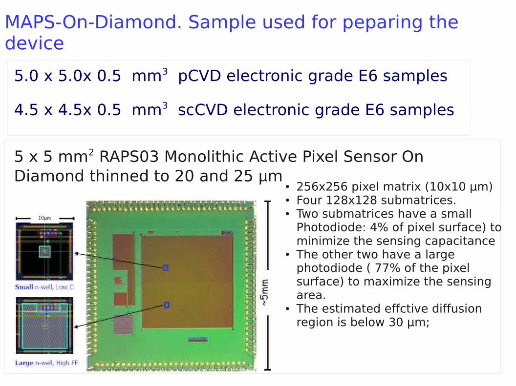
5 x 5 mm2 RAPS03 Monolithic Active Pixel Sensor On Diamond thinned to 20 and 25 µm
256x256 pixel matrix (10x10 μm) Four 128x128 submatrices. Two submatrices have a small
Photodiode: 4% of pixel surface) to minimize the sensing capacitance
The other two have a large photodiode ( 77% of the pixel surface) to maximize the sensing area.
The estimated effctive diffusion region is below 30 μm;
4.5 x 4.5x 0.5 mm3 scCVD electronic grade E6 samples
5.0 x 5.0x 0.5 mm3 pCVD electronic grade E6 samples
MAPS-On-Diamond. Sample used for peparing the device

Good diamond surface
Standard silicon
Very good diamond surface
Under this condition a uniaxial pressure of 800 atm is needed for adhesion before laser bonding
For SOD bonding the surfaces must be polished and in contact before laser processing. We choose the best polished pCVD diamond surfaces
355 nm, 20 ps, 0.4 J/cm2
Ra < 10 nm Ra < 1 nm
Ra < 1 nm
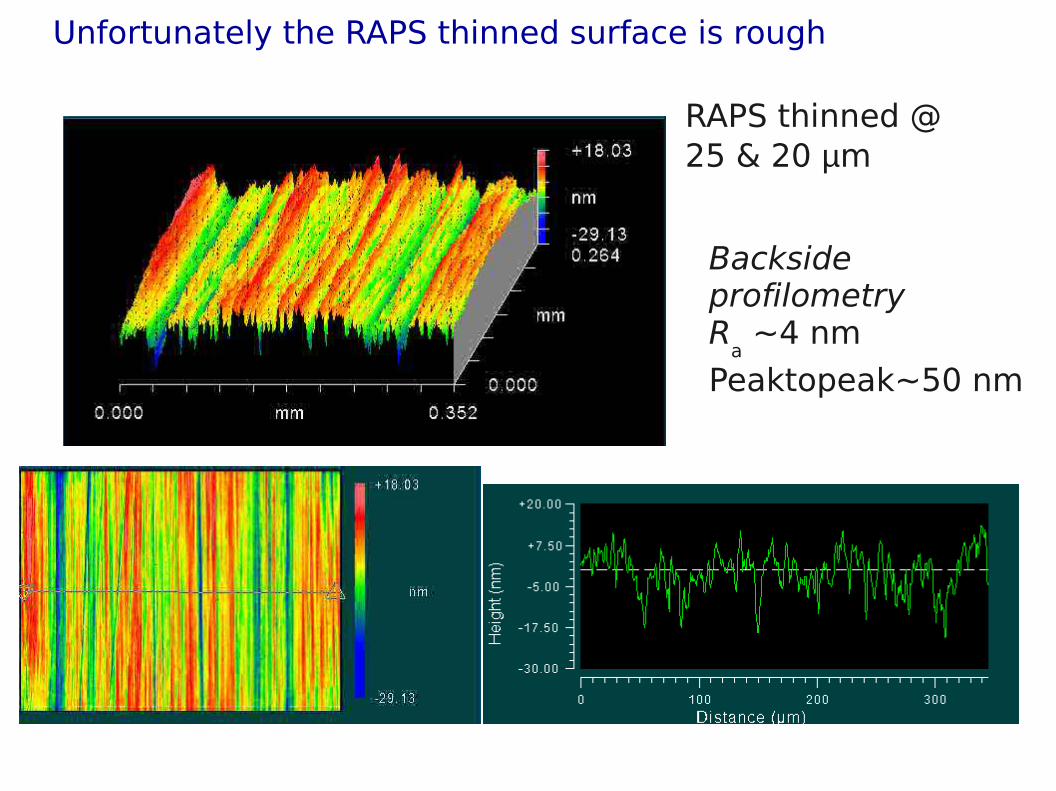
RAPS thinned @ 25 & 20 µm
Backside profilometryR
a ~4 nm
Peaktopeak~50 nm
Unfortunately the RAPS thinned surface is rough
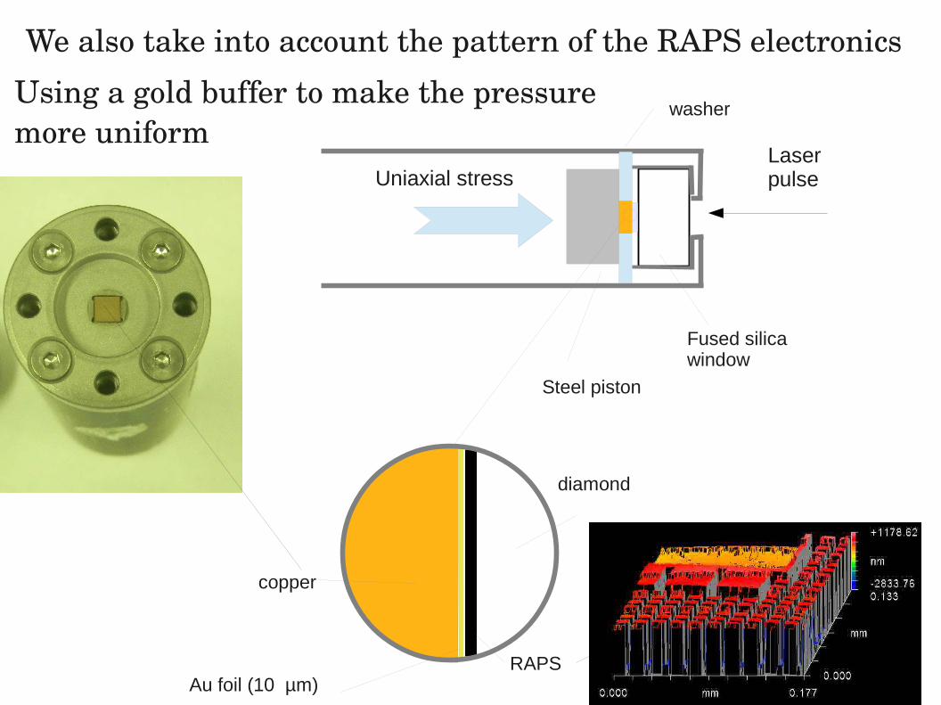
Steel piston
washer
Fused silica window
diamond
RAPSAu foil (10 µm)
copper
Laser pulseUniaxial stress
We also take into account the pattern of the RAPS electronics
Using a gold buffer to make the pressure more uniform
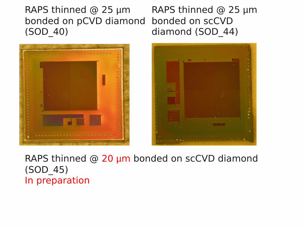
RAPS thinned @ 25 µm bonded on pCVD diamond (SOD_40)
RAPS thinned @ 25 µm bonded on scCVD diamond (SOD_44)
RAPS thinned @ 20 µm bonded on scCVD diamond (SOD_45)In preparation
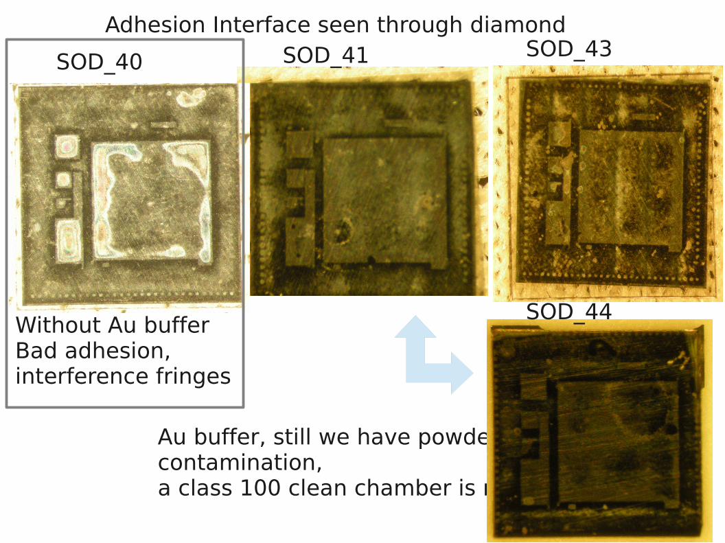
Adhesion Interface seen through diamond
SOD_40 SOD_41
Without Au bufferBad adhesion, interference fringes
Au buffer, still we have powder contamination, a class 100 clean chamber is needed
SOD_43
SOD_44
25 µm RAPS bonded to diamond succesfully (almost) all the matrix sensors working
Adhesion must be optimizedBetter polishing needed (present technology allows ultraflat surfaces at the atomic level*)Use of a class 100 clean chamber
We must increase the statistics of tested devices10 pCVD diamond samples from II-VI delivered at the end of the year We can fabricate and test one new device per month
*Beilstein J Nanotechnol. 2013 Dec 11;4:875-85. doi: 10.3762/bjnano.4.99.Challenges in realizing ultraflat materials surfaces.Yatsui T. et al. Univ. of Tokyo
CONCLUSIONS
Laser graphitization studies:
transient current measurements induced by femtosecond laser, an experimental study aimed at understanding the physics of graphitization
A deeper understanding of the process will be useful to predict the outcome at different process parameters (wavelength, intensity, pulse width, repetition rate) and to plan useful improvements of the technology.
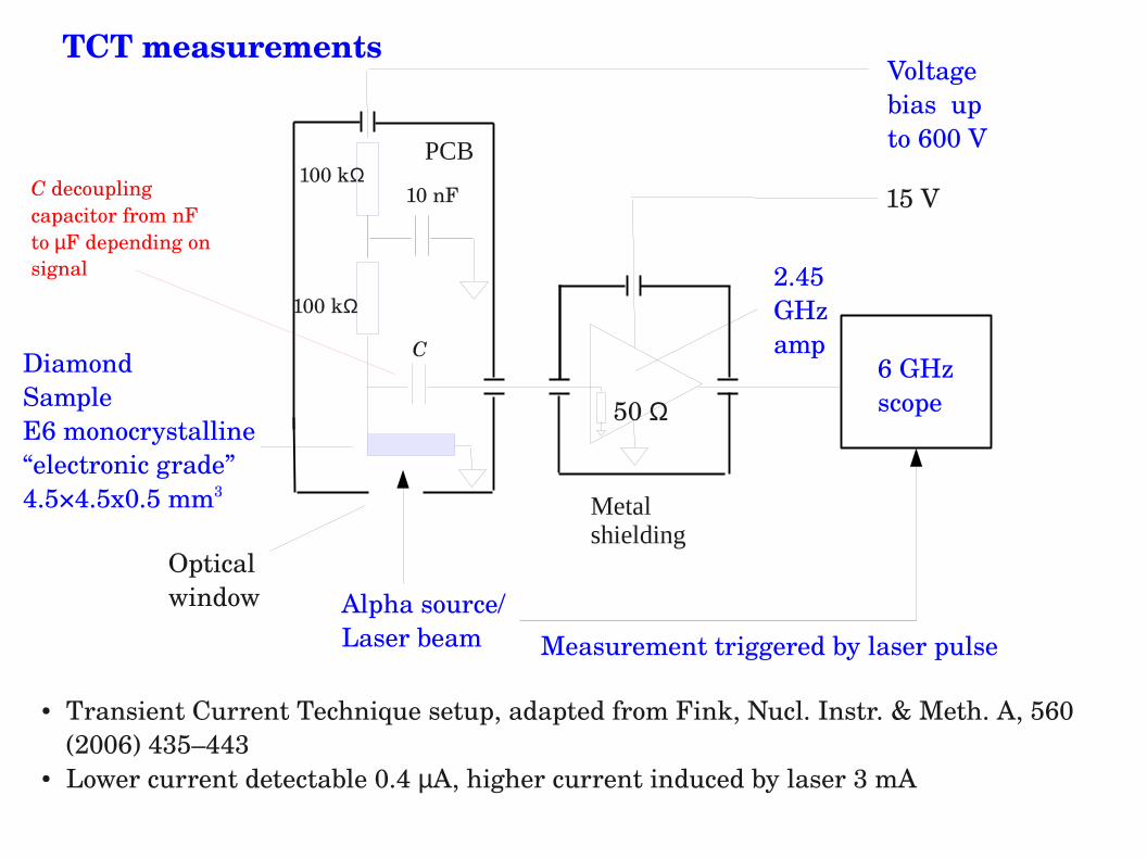
Transient Current Technique setup, adapted from Fink, Nucl. Instr. & Meth. A, 560 (2006) 435–443
Lower current detectable 0.4 µA, higher current induced by laser 3 mA
15 V
Voltage bias up to 600 V
6 GHz scope50 Ω
2.45 GHz amp
Metal shielding
Opticalwindow
DiamondSampleE6 monocrystalline“electronic grade”4.5×4.5x0.5 mm3
Alpha source/Laser beam
PCB100 kΩ
100 kΩ
10 nF
C
C decoupling capacitor from nF to µF depending on signal
TCT measurements
Measurement triggered by laser pulse
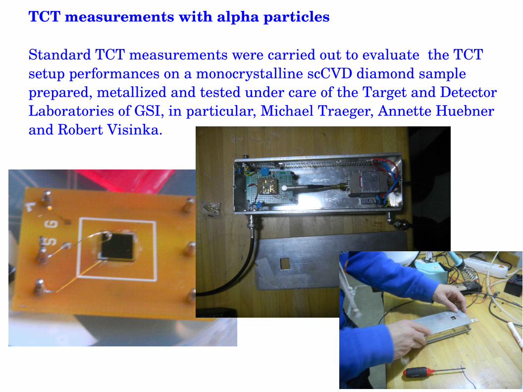
TCT measurements with alpha particles
Standard TCT measurements were carried out to evaluate the TCT setup performances on a monocrystalline scCVD diamond sample prepared, metallized and tested under care of the Target and Detector Laboratories of GSI, in particular, Michael Traeger, Annette Huebner and Robert Visinka.
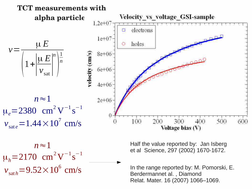
v=μ E
(1+∣μ Evsat
∣n
)1n
TCT measurements with alpha particles
n≈1μe=2380 cm2 V−1 s−1
vsat e=1.44×107 cm/s
n≈1μh=2170 cm2 V−1s−1
vsath=9.52×106 cm/s In the range reported by: M. Pomorski, E. Berdermannet al. , DiamondRelat. Mater. 16 (2007) 1066–1069.
Half the value reported by: Jan Isberg et al Science, 297 (2002) 1670-1672.
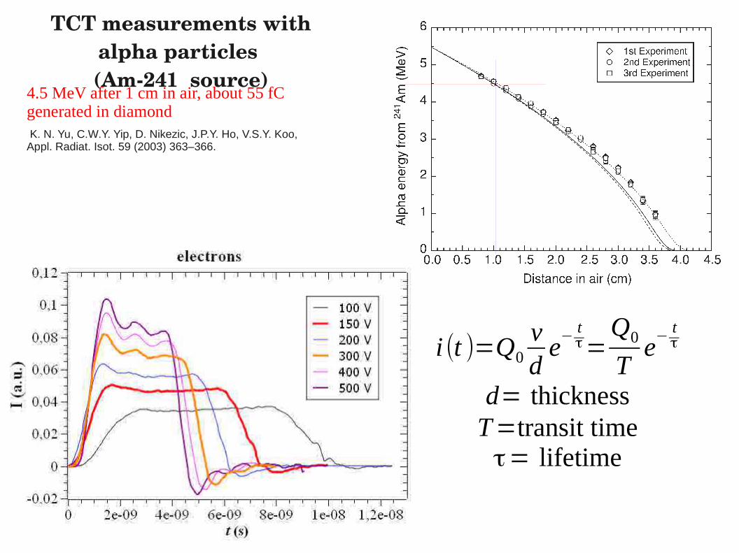
TCT measurements with alpha particles (Am241 source)
4.5 MeV after 1 cm in air, about 55 fC generated in diamond K. N. Yu, C.W.Y. Yip, D. Nikezic, J.P.Y. Ho, V.S.Y. Koo,Appl. Radiat. Isot. 59 (2003) 363–366.
i(t )=Q0vd
e−
tτ=
Q0
Te−
tτ
d= thicknessT=transit timeτ= lifetime
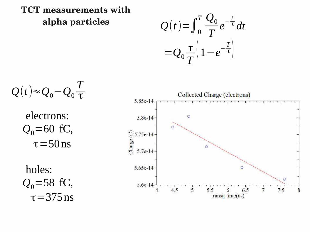
TCT measurements with alpha particles Q(t )=∫0
T Q0
Te−
tτ dt
=Q0τT
( 1−e−Tτ )
Q(t )≈Q0−Q0
Tτ
electrons: Q0=60 fC,
τ=50ns
holes: Q0=58 fC,
τ=375 ns

TCT measurements with pulsed laser source30fs modelocked Tisapphire laser (peaked at 800 nm, photon energy: 1.56 eV)Repetition rate 1 khzLaser energy per pulse: 04 µJ, focus area 50 µm
08 J/cm2 per pulse, pulse power 2.5 x10¹⁴ W/cm2 , field strength 2.3 x10¹² V/mbelow the graphitization threshold at least in the bulk
Single crystal “electronic grade” scCVDElectrodes made by superficial graphitization as a raster of colums with a 8 ns, Qswitched Nd:YAG laser
Next sample, should be equipped with standard metallizations for both alpha and laser measurements

The transit time T increases from 25 ns to 1.2 µs as the energy per pulse goes from 0.1 µJ to 4 µJ.
This is due to the high density of the plasma generated by the field and the mutual attraction of the holes and electrons.
A typical current transient shape is shown in figure at a voltage bias of 500 V.
The rising part of the current waveform can be fitted to a √t trend and the decaying part to a √(t-T) curve (with different proportionality constants).
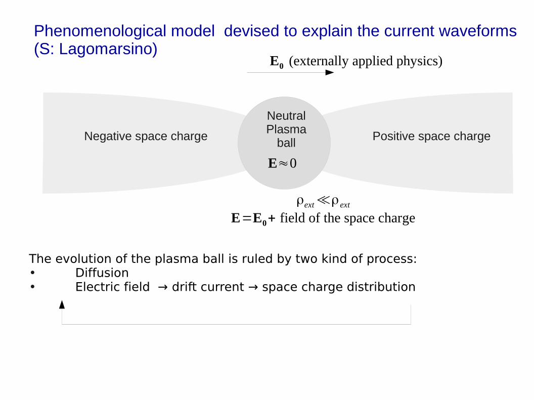
Phenomenological model devised to explain the current waveforms (S: Lagomarsino)
NeutralPlasma
ball Positive space chargeNegative space charge
ρext≪ρext
E=E0+ field of the space charge
E≈0
E0 (externally applied physics)
The evolution of the plasma ball is ruled by two kind of process:• Diffusion• Electric field → drift current → space charge distribution

M o r e o v e r , s i n c e t h e t r a n s i t t i m e << e v o l u t i o n a r y t i m e o f t h e p l a s m a b a l l , w e c a n a d o p t a q u a s i - s t a t i o n a r y a p p r o x i m a t i o n
τ is a lifetime of plasma ∼190 ns
dd R
R2=D−
μϵE02
d2π ζ
1ρ+ρ0
1ρ
dd t
ρ=−( 1τ +
3D2 R2 )
R radius of the plasma ball

Experimental plot of the carrier density vs. the energy of the pulse in a Log-Log scale. The trend before 1 J/pulse is that of a more-than-fourth power law, demonstrating a combinations of multi-photon ionization processes.
carrier density=C0×(energy per pulse)m
C0=1019 m=4.4
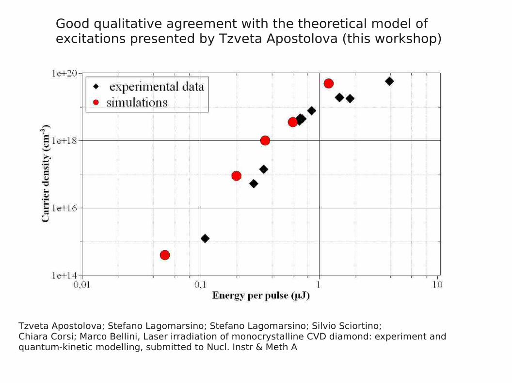
Tzveta Apostolova; Stefano Lagomarsino; Stefano Lagomarsino; Silvio Sciortino;Chiara Corsi; Marco Bellini, Laser irradiation of monocrystalline CVD diamond: experiment andquantum-kinetic modelling, submitted to Nucl. Instr & Meth A
Good qualitative agreement with the theoretical model of excitations presented by Tzveta Apostolova (this workshop)

Conclusions
Order of the process 4 and five multiphton excitation determined experimentally
The excitation theoredical model is in order-of-magnitude agreement showing that we catch the relevant physics of the process
We succesfully modeled also the decay of the laser induced plasma after the pulse
Measurements up to the graphitization threshold
Refinement of the theoretical model (Tzveta Apostolova) to predict the carrier density required for phase transitions
In a good track for fully understand the graphitization process in diamond
Thank you for listening!
Diamond device fabrication and characterization
Silvio Sciortino, Stefano Lagomarsino, Giuliano ParriniINFN and Department of Physics of Florence
GSI Darmsadt
Arianna Morozzi, Keida Kanxheri, Daniele Passeri, Leonello Servoli
INFN and University of Perugia