die-to-wafer bonding of thin dies using a 2-step approach ... · die-to-wafer bonding of thin dies...
TRANSCRIPT

Die-to-Wafer bonding of thin diesusing a 2-Step approach;
High Accuracy Placement, then Gang Bonding
Gilbert LecarpentierSET (Smart Equipment Technology), 131 impasse Barteudet, Saint Jeoire, France
Rahul Agarwal, Wenqi Zhang, Paresh Limaye, Riet Labie, A. Phommahaxay, P. SoussanIMEC, Kapeldreef 75, 3000 Leuven, Belgium
1 6th Int'l Conference & Exhibit on Device Packaging

OUTLINE
Introduction
The push towards 3D
Wafer-to-Wafer Vs Die-to-Wafer
Die to Wafer Bonding Approaches Die to Wafer Bonding Approaches
Demonstrator description
Bonding process and results
Summary
6th Int'l Conference & Exhibit on Device Packaging2

3D ASSEMBLY BY CHIP OR WAFER STACKING
Higher density 3D die-to-die interconnection has be ena major industry goal for the past decade
Multifunction Devices (heterogeneous integration)Higher Packaging MiniaturizationRepartitioning Reduces area of individual chips (Yield improvement)
Reduces number of mask levels per die (Cost reduction) Results in much shorter global interconnect lines for better
performances
6th Int'l Conference & Exhibit on Device Packaging3

3D-TSV PACKAGING FORECAST
2 500
3 000
3 500
4 000
4 500
Ma
rke
t V
alu
e (
M$
)
Breakdown per application (in M$)
Stacked NAND Flash
Wireless SiP
Logic '3D-SOC/SiP'
'Logic + Memory' SiP modules
Stacked DRAM modules
Yole Developpement © October 2009
6th Int'l Conference & Exhibit on Device Packaging4
0
500
1 000
1 500
2 000
2009 2010 2011 2012 2013 2014 2015
Ma
rke
t V
alu
e (
M$
)
Stacked DRAM modules
Power & Analog components
HB-LED modules
MEMS & sensors
CMOS image sensors

3D TECHNOLOGY EVOLUTION
Established 3D TechnologyStacked Dices interconnected using Wire bonding technology is widely used Peripheral, Long wire bonds Low-density interconnects
Memory stack with TSV Higher 3D-Interconnect density Increased performance
Shorter connectionLower Capacitance and Inductance
6th Int'l Conference & Exhibit on Device Packaging5
2006

PLACEMENT SCHEMES
Wafer-to-Wafer Bonding (W2W)
Die-to-Die (D2D / C2C)
Die-to-Wafer Bonding (D2W / D2W)
In situ Bonding
6th Int'l Conference & Exhibit on Device Packaging6
In situ Bonding
Sequential placement followed by gang bonding

CHIP TO WAFER Vs. WAFER STACKING
WAFER STACKING
High Throughput
Wafer Level
Component size must be identical
Yield ?
6th Int'l Conference & Exhibit on Device Packaging7

CHIP TO WAFER Vs. WAFER STACKING
WAFER STACKING
High Throughput
Wafer Level
Component size must be identical
Yield ?
CHIP-TO-WAFER
6th Int'l Conference & Exhibit on Device Packaging8
Lower Throughput
Single Chip Placement
High Yield
Known Good Die
Flexibility
Component size
Different Technologies

0.7
0.8
0.9
1.0
1.1
1.2
1.3
1.4
1.5
3D-S
IC c
ost p
.u.a
. fo
r 1
W2W
chi
p st
ack
($/m
m^2
)
W2W cost W2
W2W cost W1
SIC process cost W2
SIC process cost W1
Die yield loss cost
Die cost W3
Die cost W2
Die cost W1
0.7
0.8
0.9
1.0
1.1
1.2
1.3
1.4
1.5
3D-S
IC c
ost p
.u.a
. fo
r 1
D2W
chi
p st
ack
($/m
m^2
)
D2W cost W2
D2W cost W1
SIC process cost W2
SIC process cost W1
Die yield loss cost
Die cost W3
Die cost W2
Die cost W1
Cu nail Process 2x
Cost of lostGood Si-die
StackingProcess 2x
COST EFFECTIVE INTERCONNECT BONDING
W2W vs D2W bonding: trade-off between cost and align ment accuracy / TSV density requirements
0.0
0.1
0.2
0.3
0.4
0.5
0.6
0.7
12 35 59 82 106
129
153
176
200
Chip Area
3D-S
IC c
ost p
.u.a
. fo
r 1
W2W
chi
p st
ack
($/m
m^2
)
W2W
0.0
0.1
0.2
0.3
0.4
0.5
0.6
0.7
12 35 59 82 106
129
153
176
200
Chip Area
3D-S
IC c
ost p
.u.a
. fo
r 1
D2W
chi
p st
ack
($/m
m^2
)
D2WGood Si-die
Cost of 2DGood Si die3x
Assuming: Yield 1cm² die = 80%, Die yield Y = Ypua. A , Fault coverage KGD test = 90%,W2W and D2W have a 95% processing yield, Production volume 10 4 wafer stacks.
3D-SIC Cost p.u.a. = Stacked Wafer cost/(number of good 3D stacks x die area)
9 6th Int'l Conference & Exhibit on Device Packaging

HIGH ACCURACY PLACEMENTPIXEL DETECTORS: LONG HISTORY IN FINE PITCH DIE STA CKING
Small bumps (down to 5 µm)Fine Pitch (down to 10 µm)
High Accuracy Placement and Tight Parallelism Control
1978: 32x32
1988: 256x256
1992: 1k x 1k
2002: 2k X 2K
Silicon sub-board “fanout” or read out
Radiation
Indium bump
DetectorHgCdTe, GaAs, InP, etc.
Electricalsignal
For over 30 years, this application has demonstrated successful Heterogeneous Integration of Low Pitch devices with various bonding methods
10 6th Int'l Conference & Exhibit on Device Packagin g

3D-IC, ACCURACY REQUIREMENTSSIMILAR TO IR-FPA CHALLENGES: SMALL PIXEL/BUMP SIZE
Conventional flip-chip solder ball Today Tomorrow
6µ
6µ
18µ
4µ4µ
8µ
Indium-bumped IR-FPA
3D Interconnect using High Density TSV technology converge with these assembly Requirements
High Throughput Required for 3D-IC adoption, still need to be addressed
50 µ
11 6th Int'l Conference & Exhibit on Device Packagin g

COST-EFFECTIVE HYBRID D2W BONDING
Cost effective processing by segmentation of 3D ass embly process into Pick-and-Place + Collective Bonding.
Wafer-level bonding tool
TSV-die
Pick-and-place tool
Patterneddielectric glue
Wafer-level bonding toolWafer-level bonding tool
TSV-die
Pick-and-place tool
Patterneddielectric glue
TSV-die
Pick-and-place tool
Patterneddielectric glue
Enables: KGD selection Increased efficiency of 3D assembly process
Landing waferLanding wafer Landing waferLanding waferLanding waferLanding wafer
Die Pick and place Collective bonding
12 6th Int'l Conference & Exhibit on Device Packagin g

IN-SITU Vs HYBRID APPROACHDIE-TO-WAFER BONDING, TEMPERATURE PROFILE
Sequential D2W bondingTime consumingLanding wafer sees several bonding T-cycles
Temp.
Met
al b
ondi
ng
Met
al b
ondi
ng
Met
al b
ondi
ng
Temp.
Met
al b
ondi
ngD
ie 1
time
Met
al b
ondi
ngD
ie 2
Met
al b
ondi
ngD
ie n
13 6th Int'l Conference & Exhibit on Device Packagin g

IN-SITU Vs HYBRID APPROACH COLLECTIVE HYBRID BONDING, TEMPERATURE PROFILE
Temp.
Bon
ding
&
poly
mer
cur
e
Collective bonding@ wafer level
Pic
k &
pla
ce: d
ie 1
Pol
ymer
Ref
low
Wafer population@ wafer level
Bon
ding
&
poly
mer
cur
e
LT
Pic
k &
pla
ce: d
ie 1
Pol
ymer
Ref
low
time
die
2
die
n
14 6th Int'l Conference & Exhibit on Device Packagin g

D2W BONDING WITH HYBRID APPROACHIMEC DEMONSTRATOR
Top die: 25 um thick, mounted on thick carrier die
Placement on a 200mm landing wafer covered by a patterned polymer acting as a temporary alignment holder using the SET High Accuracy Die Bonder the SET High Accuracy Die Bonder model FC300 (± 0.5µm)
Bonding process: Cu/Cu (10µm pitch)
6th Int'l Conference & Exhibit on Device Packaging15
Special test structure was designed on the landing die to electrically determine the alignment accuracy after bonding - both with respect to the X-Y alignment and the rot ation
Stacks are assembled by collective hybrid bonding p rocess using wafer bonder

D2W BONDING WITH HYBRID APPROACH PICK AND PLACE
Wafer-level bonding tool
TSV-die
Pick-and-place tool
Patterneddielectric glue
Wafer-level bonding toolWafer-level bonding tool
TSV-die
Pick-and-place tool
Patterneddielectric glue
TSV-die
Pick-and-place tool
Patterneddielectric glue
Landing waferLanding wafer
glue
Landing waferLanding waferLanding wafer
glue
Landing wafer
glue
Die pick and place Collective bonding
16 6th Int'l Conference & Exhibit on Device Packagin g

D2W BONDING WITH HYBRID APPROACHCOLLECTIVE BONDING
Wafer-level bonding tool
TSV-die
Pick-and-place tool
Patterneddielectric glue
Wafer-level bonding toolWafer-level bonding tool
TSV-die
Pick-and-place tool
Patterneddielectric glue
TSV-die
Pick-and-place tool
Patterneddielectric glue
6th Int'l Conference & Exhibit on Device Packaging17
Landing waferLanding wafer
glue
Landing waferLanding waferLanding wafer
glue
Landing wafer
glue
Die pick and place Collective bonding

PLACEMENT TOOL USED FOR THE EXPERIMENTSET FC300 - HIGH ACURACY DEVICE BONDER
±±±± 0,5 µm, 3σσσσ Post-Bond Accuracy(Process dependent)
Die Bonding, Flip Chip Bonding
Large Device Bonding Capability
6th Int'l Conference & Exhibit on Device Packaging18
Device up to Sq. 100 mm Substrate up to Ø 300 mm
Process Flexibility Up to 400 kg Bonding Force Up to 450°C Heating UV-Curing, Ultra Sonic

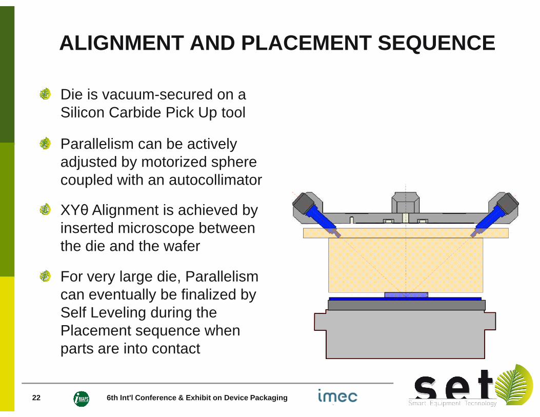
ALIGNMENT AND PLACEMENT SEQUENCE
Die is vacuum-secured on a Silicon Carbide Pick Up tool
6th Int'l Conference & Exhibit on Device Packaging19

ALIGNMENT AND PLACEMENT SEQUENCE
Die is vacuum-secured on a Silicon Carbide Pick Up tool
Parallelism can be actively adjusted by motorized sphere coupled with an autocollimator
6th Int'l Conference & Exhibit on Device Packaging20

ALIGNMENT AND PLACEMENT SEQUENCE
Die is vacuum-secured on a Silicon Carbide Pick Up tool
Parallelism can be actively adjusted by motorized sphere coupled with an autocollimator
XYθ Alignment is achieved by
6th Int'l Conference & Exhibit on Device Packaging21
XYθ Alignment is achieved by inserted microscope between the die and the wafer
ALIGNMENT AND PLACEMENT SEQUENCE
Die is vacuum-secured on a Silicon Carbide Pick Up tool
Parallelism can be actively adjusted by motorized sphere coupled with an autocollimator
XYθ Alignment is achieved by
6th Int'l Conference & Exhibit on Device Packaging22
XYθ Alignment is achieved by inserted microscope between the die and the wafer
For very large die, Parallelism can eventually be finalized by Self Leveling during the Placement sequence when parts are into contact

PICK & PLACE PERFORMANCETOOL AND MATERIAL REQUIREMENTS
Assessing Pick-and-Place performance by assessing d ie sticking Top-die Pick-and-place temperature
(landing substrate @ Room Temperature) Minimal touch-down time Minimal touch-down force Minimal touch-down force
Polymer Requirements Photo-patterning ability Adequate Adhesion to die after Photo Patterning Good deformability of patterned polymer during bonding Compatible with Cu-Cu bonding T (> 250°C)
23 6th Int'l Conference & Exhibit on Device Packagin g

POLYMER SELECTIONPATTERNING PROPERTIES
Polymer patterning: Using 1X aligner Typical cross or dot patterns Two different polymers were tested (A, B), they perform similarly
Cu padCu pad
polymer crossPolymer dots
Landingwafer
24 6th Int'l Conference & Exhibit on Device Packagin g

80
100
120
140
Top
die
T [C
]
polymer A; F=10kg; 100% stictionpolymer A; F=10kg; <100% stictionpolymer B; F=1kg; 100% stictionpolymer B; F=1kg; <100% stiction
POLYMER SELECTION PICK AND PLACE PROCESS WINDOWS
0
20
40
60
0 10 20 30 40 50 60 70Touch down [sec]
Top
die
T [C
]
Note: Landing wafer @ RT during P&P
25 6th Int'l Conference & Exhibit on Device Packagin g

80
100
120
140
Top
die
T [C
]
polymer A; F=10kg; 100% stictionpolymer A; F=10kg; <100% stictionpolymer B; F=1kg; 100% stictionpolymer B; F=1kg; <100% stiction
POLYMER SELECTION PICK AND PLACE PROCESS WINDOWS
0
20
40
60
0 10 20 30 40 50 60 70Touch down [sec]
Top
die
T [C
]
Polymer B enables strong reduction of both Force and Temperature during pick-and-place operation
Note: Landing wafer @ RT during P&P
26 6th Int'l Conference & Exhibit on Device Packagin g

COLLECTIVE BONDINGBONDING CONDITIONS
Temperature (T) and time (t) as optimized for applied polymer
Bonding Temperature = 300°C time = 15 min time = 15 min Force ~ metal area to bond
27 6th Int'l Conference & Exhibit on Device Packagin g

PICK AND PLACEAND COLLECTIVE BONDING
Die placement is performed in the SET-FC300 Die Bon derDie is picked, aligned and Placed on the wafer, sec ured by the Polymer
6th Int'l Conference & Exhibit on Device Packaging28
polymer
Cu pad
Cu nail

PICK AND PLACEAND COLLECTIVE BONDING
Gang Bonding is performed in a wafer Bonder The Polymer is reflowed while the force is increased It is a critical step as die shifting might appears
Die placement is performed in the SET-FC300 Die Bon derDie is picked, aligned and Placed on the wafer, sec ured by the Polymer
6th Int'l Conference & Exhibit on Device Packaging29
polymer
Cu pad
Cu nail

CASE STUDY: DIE TO WAFER PICK & PLACE FOR Cu-Cu HYBRID BONDING
Application: Hybrid Cu-Cu bonding for 3D stackingPrinciple: Simultaneous Metal / Dielectric BondingInclusion of Polymer dielectric Decreases sensitivity to particle inclusion Provides mechanical stability in areas with low TSV Density
Thinned Cu nail die
6th Int'l Conference & Exhibit on Device Packaging30
polymer
BEOL layers
Landing wafer
Thinned Cu nail die
~ 0.7µm
Cu pad
Polymer~ 0.7µm

DIE TO WAFER BONDED SAMPLES
Landing Wafer
Top Die
31 6th Int'l Conference & Exhibit on Device Packagin g
Landing Wafer
Top Die

ALIGNMENT ACCURACY RESULTS
Alignment accuracy result combines Pick &Place and Gang Bonding steps1.75 µµµµm ± 1 µµµµm
Measured Interconnect
Top Die
TSV
32 6th Int'l Conference & Exhibit on Device Packagin g
Measured Interconnect resistance< 50 mΩ
Landing Wafer

SUMMARY AND ACKNOWLEDGMENTS
Summary Higher density 3D die-to-die interconnection has been a major
industry goal for the past decade and is now moving to production D2W bonding with a 2-Step Hybrid Approach is a cost effective,
high yield and flexible solution for 3D-IC assembly The very low TSV – pad interconnection resistance indicates that
the process is suitable for 3D stacking applicationsthe process is suitable for 3D stacking applications
Acknowledgments Thank you to the Imec Team who ran the experiments Special thanks to Philippe Soussan for his help in putting together
this presentation
6th Int'l Conference & Exhibit on Device Packaging33