differential refractive index sensor based on photonic ... · pm structures consist of two or more...
TRANSCRIPT

1
Differential Refractive index sensor based on Photonic molecules and
defect cavities.
A. Andueza1,a,c, J. Pérez-Condeb and J. Sevillaa,c
a Department of Electrical and Electronic Engineering, Universidad Pública de Navarra, Campus
de Arrosadía, 31006, Pamplona, Spain.
b Department of Physics, Universidad Pública de Navarra, Campus de Arrosadía, 31006,
Pamplona, Spain.
c Institute of Smart Cities, Universidad Pública de Navarra (UPNA) - 31006 - Pamplona, Navarra
Abstract
We present a novel differential refractive index sensor based on arrays of photonic molecules
(PM) of dielectric cylinders and two structural defect cavities. The transmission spectrum of the
photonic structure proposed as sensor shows a wide photonic stop band with two localized
states. One of them, the reference state, is bound to a decagonal ring of cylinders and the other,
the sensing state, to the defect cavities of the lattice. It is shown that defect mode is very
sensitive to the presence of materials with dielectric permittivity different from that of the
surrounding cylinders while the state in the PM is not affected by their presence. This behavior
allows to design a device for sensing applications. A prototype of the sensor, in the microwave
region, was built using a matrix of 3x2 PM arrays made of soda-lime glass cylinders (εc= 4.5). The
transmission spectra was measured in the microwave range (8-12 GHz) with samples of different
refractive index inserted in the defect cavities. Simulations with Finite Integration time-domain
Method are in good agreement with experiments. We find that the response of the sensor is
linear. Device measurement range is determined by the dielectric constant of the cylinders that
make up the device. The results here presented in the microwave region can be extrapolated to
the visible range due to scale invariance of Maxwell equations. This make our prototype a
promising structure as sensor also in the optical range.
Keywords: Remote sensing and sensors, Photonic bandgap materials; Photonic crystals; Optical
sensing and sensors.
1. Introduction
Photonic crystals (PC) based on optical cavities offer many opportunities to create, control and
design localized photonic states. The properties of these photonic states in the cavities are
similar to those of confined electron states in atoms and we may refer to them as photonic
atoms. Thus, it is possible to define more complex structures from “photonic atoms”, termed
photonic molecules (PM), formed by a cluster of several coupled photonic atoms [1].
It has been proved that a quasi-crystalline arrangement of dielectric scatterers can present well
defined transmission frequencies inside a wide bandgap. The stop band is mainly due to global
average order shown by the quasicrystal structure [2–4], while the transmission frequencies in
the gap are generated short range structures of the quasicrystal and that resonate collectively
1 Corresponding author: [email protected]

2
at these definite frequencies. Making an analogy of the cylinders as photonic atoms, these
structures would be photonic molecules.
PM structures consist of two or more light-confining resonant cavities such as Fabry-Pérot
resonators [5], microspheres [6], microrings [7], point-defect cavities in photonic crystals
(PC) [8], microdisk [9,10], coupled-resonator optical waveguide (CROW) [11], etc. On the other
hand, more complex photonic molecules can be created from coupled Photonic Crystal Cavities
(PCC) [12]. These structures are dielectric defects in photonic crystals which generate strongly
localized states in the Photonic Band Gaps (PBG) similarly to the case of impurities in atomic
crystals [13]. PCC are a suitable medium for the control and confinement of light at scales of the
order of a light wavelength in the material. The properties of PCC make them also strong
candidates for efficient single photon generation for quantum information processing [14],
development of light emitters [13], optical waveguides [13,15] or new nonlinear optics
phenomena [16].
In addition, PM’s can be used for sensing because they are very responsive to any modification
of refractive index surrounding them, their shape and the refractive index of the resonant cavity.
Typically, a sensor based on PM’s is designed to detect the resonant shift in its frequency
response produced by the change of the refractive index of the surrounding environment.
Nowadays, there are many designs to sense and measure refractive index based on PM and
defect cavities. For instance, photonic molecules have been proposed as sensing refractive index
using dielectric microdisks [10]. Other sensor, such as microcavities in 2D arrays of PC [17],
sandwich air holes [18], waveguides defect cavities [19], double hole defects [20], ring defects
coupled resonators [21] and clusters of microparticles [22] are also successfully used to design
and fabricate optical refractive index sensors.
In this paper we present a device that takes advantage of two of the above mentioned
structures, PM and PCC in order to build a differential refractive index sensor. Our novel
proposal of refractive index sensor combines the resonance effect produced in defect cavities
and photonic molecules to design a differential sensor based on two modes, one of them
sensitive to variation of refractive index: a state strongly dependent of refractive index of the
sample and another totally independent of it. Employing these two modes we can design a
differential sensor where the value of the refractive index would be determined by difference
of the frequency value between each mode. Differential sensors provide significant advantages
over simple sensors such as cross-sensitivities reduction, interference and noise cancelation, etc.
The proposed structure is a 2D photonic crystal made of dielectric cylinders. A building block
containing a photonic molecule is repeated six times, in a 3x2 array. The structure holds two
positions (where four of the building blocks meet) that act as defect cavities. The output of the
sensor is the frequency value of two states in the gap. The frequency of one of the resonances
varies linearly with the refractive index of the material inserted in the cavities. The frequency of
the other state remains unchanged. A prototype of this sensor was built with glass cylinders and
measured in the microwave region. Numerical calculations based on Finite Integrated Method
(FIM) [23] were also performed for the same system and showed a very good agreement with
the experimental measurements.

3
2. Experimental
2.1.- Sensor design
The structure is generated by the repetition of a building block made of 30 cylinders. The
building block is taken from a periodic approximant used to generate a decagonal quasicrystal
(QC) of dielectric cylinders [2]. This structure includes a decagonal ring in the center able to hold
localized resonant states [2,3] therefore acting as a photonic molecule. One of these building
blocks is indicated by a dashed (green) line in figure 1. Its structure is fully determined by the
cylinder radius and the parameter a, because its height and width are given by:
h=a(2+2τ) and w=2���1 � τ�/4 �4 � 1/τ�� ,being τ the golden number τ= (1+√5)/2.
The building block is repeated six times forming a 3x2 array (of 191 cylinders) that forms two
cavities in the spots where four of the building blocks meet. These cavities, labeled C1 and C2,
are shown in figure 1 as solid (blue) circles. The simplest system based on this framework, a 2x2
array of building blocks (with four PMs and one cavity) was also analyzed (see supplementary
material for details in Dataset 1, ref [24]), The results were considerately worse than those of
the above-mentioned structure, so we focus in the 3x2 array.
Figure 1. Sensor design. Disposition of 191 cylinders structured as a 3x2 array of building
blocks, depicted by a green dashed box. Blue filled circles correspond to the spots where
samples of different refractive index will be inserted to be measured. These spots are in the
defect cavities (red solid line) labeled C1 and C2.
2.2. Prototype construction and characterization
A prototype of the sensor described in the previous section was fabricated with glass cylinders.
The prototype is shown in figure 2. Soda-lime glass cylinders of 3 mm radius and 250 mm length
were hold parallel to each other, fixed between two wooden pieces where their positions had
been previously carved (with a numerical control drill). The decagonal rings acting as PM present
an edge length a=12 mm with radius r=0.25a. The aspect-ratio (AR) which relates the length and

4
the diameter of the cylinders, it is 42, approximately. The dispersion for radius of cylinders was
also measured, found to be less than 0.2% of the nominal value, 3mm.
The cylinders dielectric permittivity at microwave frequencies was estimated at εc=4.5 as follows:
first, we fabricated and measured the transmission spectra in perpendicular incidence, with TE
(transversal electric) and TM (transversal magnetic) polarizations, of triangular and square
regular lattices. Then we compared these results with simulations of the both structures and
both polarization with the dielectric constant as only free parameter; the best fit was found for
εc=4.5.
In order to analyze the performance of the prototype as a sensor, transmission spectra were
measured after inserting cylinders of different materials (with different dielectric permittivity
values) at the sensing positions (solid blue circles in figure 1).
Fig. 2. (a) Image of the built-up glass sensor completed with axis notation used in the text. (b)
Detail of the fabricated sensor indicating the building block, defects cavities and cylinders
samples
Transmission spectra were measured using a vector network analyzer (VNA) HP 8722ES spliced
to rectangular horn antennas 79mm × 46mm (Narda Model 640), aligned and separated
approximately 400 mm from each other. The sample is placed in the space between the
antennas, with the cylinders perpendicular to the incidence direction [25]. The measurement
bandwidth is similar to antennas one and ranges from 8 GHz to 12 GHz. The cylinder and
dielectric permittivity of the samples were selected in order to tune the modes in the bandwidth
of the experimental setup. A differential measurement technique was used to register the
transmission spectra. First, the transmission spectrum without the sample was recorded on the
network analyzer. Next, the transmission spectrum of structure was measured. The analyzer
automatically provided the difference between the spectra with and without the sample. A
smoothing algorithm Savithzky-Golay from VNA (span for the moving average of 6 samples) was
used to reduce the ripple noise of the measurements due to the finite size of the sensor.
In this work we consider the transverse magnetic (TM) polarization of the incident radiation,
with the electric field vector parallel to the cylinders axis. The influence on the measurements
of these drilled wooden pieces supporting the cylinders is negligible since the cylinders have a
length of 25 cm and the antenna aperture never exceed 20 cm at 12 GHz.

5
Numerical calculations were carried out with CST MICROWAVE STUDIO™, a commercial code
based on the Finite Integration time-domain Method (FIM) [23]. This program is an
electromagnetic field sG:\LACIE\Memoria_PC\papers\Rosetas\manuscrito\obsoletoimulation
software package especially suited for analysis and design in the high-frequency range.
Considering the radiation traveling in the z direction, a Transverse Electric and Magnetic (TEM)
mode with the electric field along x-axis and the magnetic field along y-axis was injected at
normal incidence on the sensor. The symmetry of the sensor and the orientation of the
electromagnetic field allow us to simplify the problem restricting the calculation to a unit cell
consisting of one and a half consecutive building blocks. In our case two symmetry planes are
considered, xy and xz. Every symmetry plane reduces the calculation time by a factor of 2.
3. Results and discussion
3.1. Calibration curve
In the sensor prototype here proposed, the variable that encodes the measurand (refractive
index of a sample) is the frequency of the sensing state. To ease the calibration of this sensing
state, the sensor presents another state, the reference state, which remains unaltered for
variations of the measurand. The calibration curve of the sensor was obtained by simulating the
transmission spectrum of the structure for different values of the dielectric permittivity εs of the
samples inserted in the sensing spots. Two types of samples have been considered: (i) cylinders
of the same radius of the rods composing the sensor (r2=3 mm), and (ii) thinner cylinders (r2=2.5
mm). The results are presented as 3D color maps in figure 3. The vertical axis represent the
frequency (ranging from 9 to 12 GHz), the horizontal axis depicts the dielectric permittivity εs of
the samples (ranging from εs=1 to εs=5.5) while the transmitted intensity for each case is
presented as the color of the points in the plot (and varies from 0 to -30 dB related to full
transmission).
Figure 3. Colormap plots of the calculated transmission spectra (dB) as a function of frequency
(f) and dielectric permittivity (εs) of the samples at the cavities C1 and C2 with a radius of (a)
r2=3 mm and (b) r2=2.5. Dielectric permittivity and length of the cylinders are εc=4.5 and l=25
cm, respectively. Horizontal yellow lines at 10.57 GHz correspond to reference mode of the
sensor. Oblique yellow/cyan lines correspond to sensing mode. Vertical white-dashed line
corresponds to experimental measurements.
In Figure 3 we see that the sensing mode frequency decreases linearly with the mesurand value
(εs). In contrast, the reference mode do not change for any dielectric permittivity value. The
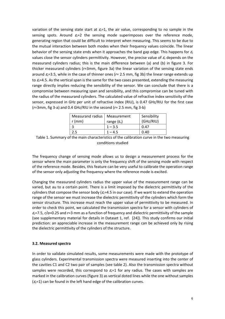
6
variation of the sensing state start at εs=1, the air value, corresponding to no sample in the
sensing spots. Around εs=2 the sensing mode superimposes over the reference mode,
generating region that could be difficult to interpret when measuring. This seems to be due to
the mutual interaction between both modes when their frequency values coincide. The linear
behavior of the sensing state ends when it approaches the band gap edge. This happens for εs values close the sensor cylinders permittivity. However, the precise value of εs depends on the
measurand cylinders radius; this is the main difference between (a) and (b) in figure 3. For
thicker measurand cylinders (r=3mm, figure 3a) the linear variation of the sensing state ends
around εs=3.5, while in the case of thinner ones (r= 2.5 mm, fig 3b) the linear range extends up
to εs=4.5. As the vertical span is the same for the two cases presented, extending the measuring
range directly implies reducing the sensibility of the sensor. We can conclude that there is a
compromise between measuring span and sensibility, and this compromise can be tuned with
the radius of the measurand cylinders. The calculated value of refractive index sensitivity of the
sensor, expressed in GHz per unit of refractive index (RIU), is 0.47 GHz/RIU for the first case
(r=3mm, fig 3-a) and 0.4 GHz/RIU in the second (r= 2.5 mm, fig 3-b)
Measurand radius
r (mm)
Measurement
range (εs)
Sensibility
(GHz/RIU)
3 1 – 3.5 0.47
2.5 1 – 4.5 0.40
Table 1. Summary of the main characteristics of the calibration curve in the two measuring
conditions studied
The frequency change of sensing mode allows us to design a measurement process for the
sensor where the main parameter is only the frequency shift of the sensing mode with respect
of the reference mode. Besides, this feature can be very useful to calibrate the operation range
of the sensor only adjusting the frequency where the reference mode is excited.
Changing the measurand cylinders radius the upper value of the measurement range can be
varied, but au to a certain point. There is a limit imposed by the dielectric permittivity of the
cylinders that compose the sensor body (εc=4.5 in our case). If we want to extend the operation
range of the sensor we must increase the dielectric permittivity of the cylinders which form the
sensor structure. This increase must reach the upper value of permittivity to be measured. In
order to check this point, we calculated the transmission spectra for a sensor with cylinders of
εc=7.5, r/a=0.25 and r=3 mm as a function of frequency and dielectric permittivity of the sample
(see supplementary material for details in Dataset 1, ref. [24]). This study confirms our initial
prediction: an appreciable increase in the measurement range can be achieved only by rising
the dielectric permittivity of the cylinders of the structure.
3.2. Measured spectra
In order to validate simulated results, some measurements were made with the prototype of
glass cylinders. Experimental transmission spectra were measured inserting into the center of
the cavities C1 and C2 two pair of samples (see table 2). Also the transmission spectra without
samples were recorded, this correspond to εs=1 for any radius. The cases with samples are
marked in the calibration curves (figure 3) as vertical doted lines while the one without samples
(εs=1) can be found in the left hand edge of the calibration curves.

7
Sample Simulated results (Frequencies)
Measured results
(Frequencies)
Experimental
configuration Radius
(mm) εs
Reference
state (GHz)
Sensing
state A
(GHz)
Sensing
state B
(GHz)
Reference
state
(GHz)
Sensing
state A
(GHz)
Sensing
state B
(GHz)
1 2.5 4.0 10.57 9.78 Not
visible 10.70 9.69
Not
visible
2 3 4.5 10.57 Not
visible
Not
visible 10.70
Not
visible
Not
visible
3 Any 1.0 10. 57 11.04 11.12 10.70 11.11 11.22
Table 2. Summary of the performed measurements
The results, together with the simulations of the same structures, are presented in figures 4
(measurements 1 and 3) and figure 5 (measurements 2 and 3). In general the correspondence
between measurements and simulations is quite good. The spectra show the transmission stop
band from 9.5 GHz to about 12 GHz, indicated with vertical dashed lines in the figures. Inside
the stop band we can observe sharp and distinct experimental peaks. Although the peaks are
sharper in the calculated results, the correspondence with the observed ones is remarkable.
One of the states is present in all the measurements, this is the reference state and has been
labeled R. It is interesting to note that the other state, the one that is dependent on the εs value,
is really composed of two different peaks almost overlapping. This is particularly evident in the
case without sample (labeled measurement 3), where the two peaks can be seen both, in the
measurement and the calculation (labelled in the figures S3A and S3B).
Figure 4. (a) Calculated and (b) measured transmission spectra for the experimental
configurations 3 (black solid line) and 1 (red dashed line). Resonances corresponding to the
sensing (S marked) and reference modes (R marked) are labeled for each case.

8
In the case of sample 2 (figure 5) the sensing state is not detected. This happens because the
shifting in the state frequency value is big enough to move it outside the gap, making it
indistinguishable of the gap edges as can be observed in the calibration curve (figure 3a).
The frequency values of the measured and simulated peaks are summarized in table 2. The
difference between the measured and the calculated values is around 0.1 GHz (0.13 and 0.09 in
the reference and sensing states respectively). The relative error in frequency is around 1 %.,
The results can be considered an excellent proof of concept of the working principle of the
proposed sensor taking into account the fabrication tolerances of the prototype.
The influence of AR of the cylinders was analyzed (see supplementary material for details in
Dataset 1, ref. [24]). The aspect-ratio does not produce significant variations in the performance
of the sensor when it is larger than 20. Therefore, this result validates the choice of cylinders
with length of 25 cm (AR of 42).
Figure 5. (a) Calculated and (b) measured transmission spectra for the experimental
configurations 3 (black solid line) and 2 (red dashed line). Resonances corresponding to the
sensing (S marked) and reference modes (R marked) are labeled for each case. Vertical dashed
lines correspond to the edge of the stop band.
3.3. Field distribution of the resonant states
The results suggest that two resonance phenomena occurs simultaneously, exciting the
reference and sensing modes. Also, it has been found that the sensing mode is twofold in some
cases at least. In order to assess the origin of these modes we explore the calculated electric
field distributions of the system. We compute the spatial distribution of the electric field of the
modes in the gap seen in figure 4. For the calculation, polarized radiation in the x direction with

9
unit amplitude propagates in the z direction. The obtained electric field distributions are
depicted in figure. 6.
Electric field distributions of modes R1 [figure 6(a)] and R2 [figure 6(b)] are very similar, with the
electric field localized mainly inside the cylinders; with the exception of the cylinders along the
z axis where the electric field is located between them. This field pattern was previously reported
[2,3] and corresponds to a localized state presents in a decagonal quasicrystal. Therefore we can
conclude that the reference modes R1 and R2 are excited by the photonic molecules from the
decagonal ring. The electric field distribution of sensing modes S3A and S3B (at 11.04 GHz and
11.12 GHz) are plotted in figure 6(b) and 6(c), respectively, while figure 6(e) corresponds to the
sensing mode S1 at 9.9 GHz. It is important to note that the electric field pattern in S3 is strongly
localized and enhanced on each cavity and presents even or odd symmetry along y-axis for the
A and B states respectively. These kind of bonding and antibonding states in photonic crystals
has been previously reported after the introduction of an air defect into the crystal [26,27]. In
the case of S1 (found at 9.9 GHz and corresponding to the case of a sample with εs=4) the electric
field distribution is similar to the S3 case, but only the bonding state is found. The antibonding
mode is not excited when the refractive index of the sample cylinders has increased.
Figure 6. Distribution of the electric-field for yz plane (a) of R1 at f = 10.57 GHz, (b) of S1 at f =
11.04 GHz and (c) S2 at f = 11.12 GHz without a sample. (d) Distribution of the electric-field for
yz plane of R2 at f = 10.57 GHz and (e) S3 at f = 9.78 GHz for a sample of r2 = 2.5 mm and εc = 4.
The red and blue colors indicate the electric field intensity and polarity.
These results prove that this photonic structure presents sufficient capability to operate as
refractive index sensor. In addition, the existence of a reference state allows the design of a
differential version of the sensor. This differential operation provides multiple advantages such
as systematic error cancelation, cross sensitivities reduction, etc. We have also shown that
system parameters, such as size and dielectric permittivity of cylinders sets, structures and
samples, can be fitted in order to optimize its response for a given measurement range. As the
Maxwell equations governing the studied system are scale invariant, the results in the microwave
regime can readily be extrapolated to the optic range. This transformation implies that the size
of the materials and the wavelength are scaled with the same factor. Accordingly, the dielectric
permittivity in the microwave range must be considered in the optical range, taking into account
the imaginary part (which represents material losses) that can be neglected in the microwave
range but rarely in optics. Materials as Titania (TiO2), Alumina (Al2O3) or Silicon Carbide (SiC)

10
could be used for THz and FIR, or Silicon (Si) and Zinc Sulfide (ZnS) for NIR and visible zones.
4. Conclusions
We have designed and fabricated a differential refractive index sensor prototype based on 3x2
photonic molecules array of dielectric cylinders containing two defect cavities. The building
block is based on a quasi-crystaline approximant including a decagonal ring of cylinders acting
as photonic molecule. This structure creates a stop band where two modes can be excited: the
first mode is due to the PM (reference mode) and the second mode is due to the defect cavities
(sensing mode). When the defect cavity is disturbed by a sample cylinder with different dielectric
constant to the surrounding, the sensing mode suffers a frequency shift proportional to its
permittivity value. However, the reference mode associated to the photonic molecule does not
undergoes a frequency change and remains unaltered. Therefore, the dielectric permittivity can
be calculated as the frequency difference between both resonances.
Transmission spectra for two samples with different dielectric permittivity were experimentally
obtained in microwave region for a sensor fabricated with glass cylinders of permittivity εs = 4.5
and r = 3 mm. They were in good agreement with the results of the numerical calculation of the
sensor. The sensor presents a linear dependence with the refractive index of the sample in the
cavity as well as a sensitivity of 0.47 GHz/RIU and 0.4 GHz/RIU for two samples with r = 3 mm
and r = 2.5 mm, respectively. We found that the uncertainty of the sensor is lower than 5% for
the experimental measurement. However, the span of the sensor was limited by the dielectric
constant of the PM cylinders. The range of measurement can be expanded increasing the
dielectric permittivity of the surrounding cylinders.
We believe that this device is well suited to design and develop a variety of novel refractive index
optical sensors, as the scale invariance of electromagnetic waves allows the extrapolation of this
sensor to the optical and nanoscale region as well.
Acknowledgements
This work has been supported from Ministerio de Economía y Competitividad of Spain via Project
TEC2014-51902-C2-2-R. The authors would also like to thank Santiago de Miguel for his technical
support.
References
1. M. Bayer, T. Gutbrod, J. Reithmaier, a. Forchel, T. Reinecke, P. Knipp, a. Dremin, and V.
Kulakovskii, "Optical Modes in Photonic Molecules," Phys. Rev. Lett. 81, 2582–2585
(1998).
2. K. Wang, "Light localization in photonic band gaps of quasiperiodic dielectric
structures," Phys. Rev. B 82, 045119 (2010).
3. K. Wang, "Structural effects on light wave behavior in quasiperiodic regular and
decagonal Penrose-tiling dielectric media: A comparative study," Phys. Rev. B 76,
085107 (2007).
4. K. Wang, "Light wave states in two-dimensional quasiperiodic media," Phys. Rev. B -
Condens. Matter Mater. Phys. 73, 1–5 (2006).
5. A. Armitage, M. S. Skolnick, A. V. Kavokin, D. M. Whittaker, V. N. Astratov, G. A.
Gehring, and J. S. Roberts, "Polariton-induced optical asymmetry in semiconductor

11
microcavities," Phys. Rev. B - Condens. Matter Mater. Phys. 58, 15367–15370 (1998).
6. B. M. Möller, U. Woggon, M. V. Artemyev, and R. Wannemacher, "Photonic molecules
doped with semiconductor nanocrystals," Phys. Rev. B 70, 115323 (2004).
7. P. T. Rakich, M. A. Popović, M. Soljačić, and E. P. Ippen, "Trapping, corralling and
spectral bonding of optical resonances through optically induced potentials," Nat.
Photonics 1, 658–665 (2007).
8. K. A. Atlasov, K. F. Karlsson, A. Rudra, B. Dwir, and E. Kapon, "Wavelength and loss
splitting in directly coupled photonic-crystal defect microcavities," Opt. Express 16,
16255 (2008).
9. S. Ishii and T. Baba, "Bistable lasing in twin microdisk photonic molecules," Appl. Phys.
Lett. 87, 181102 (2005).
10. S. V. Boriskina, "Spectrally engineered photonic molecules as optical sensors with
enhanced sensitivity: a proposal and numerical analysis," J. Opt. Soc. Am. B 23, 1565
(2006).
11. A. Yariv, Y. Xu, R. K. Lee, and A. Scherer, "Coupled-resonator optical waveguide: A
proposal and analysis," Opt. Lett. 24, 711–713 (1999).
12. S. Vignolini, F. Intonti, M. Zani, F. Riboli, D. S. Wiersma, L. H. Li, L. Balet, M. Francardi, A.
Gerardino, A. Fiore, and M. Gurioli, "Near-field imaging of coupled photonic-crystal
microcavities," Appl. Phys. Lett. 94, 151103 (2009).
13. S. Noda, M. Fujita, and T. Asano, "Spontaneous-emission control by photonic crystals
and nanocavities," Nat. Photonics 1, 449–458 (2007).
14. J. Vučković and Y. Yamamoto, "Photonic crystal microcavities for cavity quantum
electrodynamics with a single quantum dot," Appl. Phys. Lett. 82, 2374 (2003).
15. M. Loncar, T. Doll, J. Vuckovic, and A. Scherer, "Design and fabrication of silicon
photonic crystal optical waveguides," J. Light. Technol. 18, 1402–1411 (2000).
16. M. Soljačić and J. D. Joannopoulos, "Enhancement of nonlinear effects using photonic
crystals," Nat. Mater. 3, 211–219 (2004).
17. E. Chow, A. Grot, L. W. Mirkarimi, M. Sigalas, and G. Girolami, "Ultracompact
biochemical sensor built with two-dimensional photonic crystal microcavity," Opt. Lett.
29, 1093 (2004).
18. X. Wang, Z. Xu, N. Lu, J. Zhu, and G. Jin, "Ultracompact refractive index sensor based on
microcavity in the sandwiched photonic crystal waveguide structure," Opt. Commun.
281, 1725–1731 (2008).
19. D. F. Dorfner, T. Hürlimann, T. Zabel, L. H. Frandsen, G. Abstreiter, and J. J. Finley,
"Silicon photonic crystal nanostructures for refractive index sensing," Appl. Phys. Lett.
93, 181103 (2008).
20. L. A. Shiramin, R. Kheradmand, and A. Abbasi, "High-sensitive double-hole defect
refractive index sensor based on 2-D photonic crystal," IEEE Sens. J. (2013).
21. L. Huang, H. Tian, D. Yang, J. Zhou, Q. Liu, P. Zhang, and Y. Ji, "Optimization of figure of
merit in label-free biochemical sensors by designing a ring defect coupled resonator,"
Opt. Commun. 332, 42–49 (2014).
22. A. Francois and M. Himmelhaus, "Optical biosensor based on whispering gallery mode

12
excitations in clusters of microparticles," Appl. Phys. Lett. 92, 141107 (2008).
23. M. Clemens and T. Weil, "Discrete Electromagnetism with the Finite Integration
Technique," Prog. Electromagn. Res. 32, 65–87 (2001).
24. A. Andueza, "Supporting material: Differential Refractive index sensor based on
Photonic molecules and defect cavities," figshare
https://osapublishing.figshare.com/s/e6bb98ccb3edc47f0cc9 [retrieved 25 April 2016]
(2016).
25. A. Andueza, R. Echeverría, P. Morales, and J. Sevilla, "Geometry influence on the
transmission spectra of dielectric single layers of spheres with different compactness.,"
J. Appl. Phys. 107, 124902 (2010).
26. N. Caselli, F. Intonti, F. Riboli, A. Vinattieri, D. Gerace, L. Balet, L. H. Li, M. Francardi, A.
Gerardino, A. Fiore, and M. Gurioli, "Antibonding ground state in photonic crystal
molecules," Phys. Rev. B 86, 035133 (2012).
27. S. Vignolini, F. Riboli, F. Intonti, D. S. Wiersma, L. Balet, L. H. Li, M. Francardi, A.
Gerardino, A. Fiore, and M. Gurioli, "Mode hybridization in photonic crystal molecules,"
Appl. Phys. Lett. 97, 063101 (2010).