differential signal conditioning circuit for current and
TRANSCRIPT

2V5_REF
1V25_REF
2V5FluxgateSensor
All 3-phase fluxgate sensor outputs are summed together and given as inputs to these comparators
VTH
VTH
VTL
VTLOvercurrent Indication
Earth Fault Indication
'HOILQR�
F2837x
TLC372
TLC372
ADS7854
Optional SPI Connection for External Motor Controller
×4 REF5025+ OPA322
TLV70033
TPS7A4700
REF2025
6-V DC input
×3
×2
MOTOR
TIDA-00201
DC BUS_P
DC BUS_M
DC-Link Current
R Y B
3V3
5 V
THS4531 ×4
TI DesignsDifferential Signal Conditioning Circuit for Current andVoltage Measurement Using Fluxgate Sensors
TI Designs Design FeaturesTI Designs provide the foundation that you need • Designed to Measure All 3-Phase Motor Currentsincluding methodology, testing and design files to Along With DC-Link Current through 6-A Fluxgatequickly evaluate and customize the system. TI Designs Sensor (Scalable up to 50 A)help you accelerate your time to market. • Differential Signal Conditioning Circuit to Interface
Fluxgate Sensors With Differential ADCsDesign Resources• Two Onboard 14-Bit Dual-Channel Simultaneous
Sampling SAR ADCs With 4-Wire SPI to InterfaceTool Folder Containing Design FilesTIDA-00201With External Motor ControllersTHS4531 Product Folder
• Provision to Measure Current and Voltage ThroughADS7254 Product FolderInternal ADCs of TI Delfino™ Controller F2837xADS7854 Product Folder
• <0.1% DC Accuracy of Signal Conditioning CircuitTPS7A4700 Product FolderTLV70033 Product Folder • Overcurrent and Earth Fault Protections for EachREF5025 Product Folder Channel With <100-ns Sensing DelaysREF2025 Product Folder • Provision to Interface the Signal ConditioningTLC372 Product Folder Circuit With External ADCOPA322 Product Folder
Featured ApplicationsF3837x Control Card Tool Folder
• AC Variable Speed and Servo Motor Drives• Static ConvertersASK Our E2E Experts
WEBENCH® Calculator Tools • DC Motor Drives• UPS Systems• Solar Inverters• Power Supplies for Welding Applications
An IMPORTANT NOTICE at the end of this TI reference design addresses authorized use, intellectual property matters and otherimportant disclaimers and information.
All trademarks are the property of their respective owners.
1TIDU569–October 2014 Differential Signal Conditioning Circuit for Current and Voltage MeasurementUsing Fluxgate SensorsSubmit Documentation Feedback
Copyright © 2014, Texas Instruments Incorporated

A
A
B B
C
C
CM
A) Current measurement in the DC- and DC+ link
B) Current measurement in the bottom side emitter path of each half-bridge
C) Current measurement in the output phases
3~
B
System Description www.ti.com
1 System DescriptionCurrent measurement is an inherent part of any inverter-driven application. One important reason formeasuring the motor current is to control algorithm. Vector control and direct torque control require currentsensing for control purposes. Approaches for sensorless control require the motor current measurement toprovide accurate control with low cost and complexity. Information of motor parameters is important forseveral control schemes. Stator current measurement is used for the estimation of these parameters.Motor current information is also required to detect the motor’s insulation condition. Electrical insulation isthe most critical component for operating electrical motors. Stator insulation failure during motor operationcan lead to motor failure, resulting in a costly outage.
Another important phenomenon is protection from hardware overload and earth fault conditions. Typically,these conditions occur when the current exceeds the limit of 200% or 300% of its nominal current.Derating must be taken into account when using the drive in different conditions. Ambient temperature orother environmental conditions such as dust or humidity are unknown, especially when a drive is notinstalled by the end-user but the machine manufacturer. The end user must identify all derating factors toreach a reliable solution.
Above the drive-designed ambient temperature, drives can usually operate when the maximum outputcurrent is derated according to the user’s manual of the drive. The switching frequency also playsimportant role. The higher the switching frequency of the drive is, the more the power semiconductorsgenerate heat losses. Therefore, the drive output current is derated when increasing the switchingfrequency, which applies to nominal current, overload current, and maximum instantaneous current.
The motor current can be measured at different points in the inverter. Figure 1 shows the overview ofusual measurement locations, considering a 3-phase inverter for a motor control application:
Figure 1. Typical Measuring Locations for Current Measurement in Motor Drives
2 Differential Signal Conditioning Circuit for Current and Voltage Measurement TIDU569–October 2014Using Fluxgate Sensors Submit Documentation Feedback
Copyright © 2014, Texas Instruments Incorporated
www.ti.com Design Requirements
From Figure 1, the least expensive variant of current measurement (A) is often used for applications in thelower power range. Typically, the current measurement is done on DC-MINUS bus, because this may bethe reference potential of the microcontroller and is therefore not necessary to isolate the signal. Anotheralternative location of current measurement, found particularly in the low-to-medium power range is variantB. In this case, the current is measured at the emitter of the bottom IGBT of each arm in a 3-phaseinverter. The end user can also dispense with third current measurement as this can be derived bycalculation based on the two measured current signals. The advantage of this measurement method issimilar to that of variant a, in that the negative section of the DC-bus can be taken as the commonreference potential. However, the disadvantage is the increased stray inductance. In high dynamic drivesand high-power applications, current is usually measured in the output phases of the inverter (variant C inFigure 1). The third current sensor is not necessary in this case either.
The design TIDA-00201 is predominantly meant for current measurement using fluxgate sensors in ACmotor drives, but the design can also be used for DC drives. The objective of this design is to provide asolution for differential signal conditioning circuit along with ADC to measure motor current using fluxgatesensors, typically available from companies like LEM Technologies and VACUUMSCHMELZE. It is verycommon to use single-ended ADCs integrated into the controller for current measurement. Single-endedmeasurements are more prone to noise in a larger drive system, which can lead to inaccuracies in themeasurement. Differential measurement would help to overcome the noise issues. With the Delfino seriesof controllers (consisting of differential input ADCs) from Texas Instruments (TI), it is possible to domeasure differentials overcoming noise issues.
The signal conditioning circuit for fluxgate current sensors is required for the following reasons:• Fluxgate sensors have inherent noise at 450 kHz / 900kHz because of the internal oscillator and
switching, so proper filtering is required.• Typical fluxgate sensors have a reference signal on REF pin (always at 2.5 V) and signal output
available on the OUT pin (±0.625 V riding on a 2.5-V reference). The output voltage of fluxgatesensors may not match the input range of analog-to-digital converters, or ADCs (external or internal tothe controller). In this scenario, level shifting may be required.
• Fluxgate sensors can measure up to 300% of their nominal rating. It is important to detect the overloadcondition and protect the drive.
• For a fluxgate sensor with nominal current (In) of 6 A with 300% of nominal current rating, the signalstrength can vary from 0.625 V [2.5 – (3 × 0.625)] to 4.375 V [2.5 + (3 × 0.625)]. However, the ADCsintegrated into microcontrollers can take 0 to 3.3 V, so level shifting is required.
• If using differential ADC inside Delfino controllers, the common-mode voltage needs to be shifted from2.5 V to 1.25 V, unlike the external ADCs.
2 Design Requirements• To measure a 3-phase motor current and DC-Link current in a variable speed drive using fluxgate
sensor (up to 6 A)• Signal conditioning circuit with 0.1% accuracy to interface with a differential ADC• Simultaneous sampling of all current channels• Hardware overload detection within < 100 ns• Hardware earth fault detection within < 100 ns
3TIDU569–October 2014 Differential Signal Conditioning Circuit for Current and Voltage MeasurementUsing Fluxgate SensorsSubmit Documentation Feedback
Copyright © 2014, Texas Instruments Incorporated

2V5_REF
1V25_REF
2V5FluxgateSensor
All 3-phase fluxgate sensor outputs are summed together and given as inputs to these comparators
VTH
VTH
VTL
VTLOvercurrent Indication
Earth Fault Indication
'HOILQR�
F2837x
TLC372
TLC372
ADS7854
Optional SPI Connection for External Motor Controller
×4 REF5025+ OPA322
TLV70033
TPS7A4700
REF2025
6-V DC input
×3
×2
MOTOR
TIDA-00201
DC BUS_P
DC BUS_M
DC-Link Current
R Y B
3V3
5 V
THS4531 ×4
Block Diagram www.ti.com
3 Block DiagramThe system block diagram is shown in Figure 2. There are four fluxgate current sensors used in thedesign: three for the motor phase currents and one for measuring the current flowing through the DC-Link.Each of the sensors is interfaced with a fully-differential amplifier (FDA), THS4531. The outputs of eachTHS4531 are:1. Connected to onboard 14-bit SAR ADCs (ADS7854), the digital output of which is taken out on a
connector to interface with external motor controllers or processors2. Connected to 180-pin connector to interface with Internal ADC of Delfino F2837x
To provide protection against overcurrent fault condition, each of the phases is provided with two fastresponding comparators TLC372 (one for detection of overcurrent in a positive half-cycle and one fordetection of overcurrent in a negative half-cycle). For ground fault detection, the output signals comingfrom each of the phases are combined together and compared against references using two comparatorsTLC372s. Both the protection circuits have a response time of less than 100 nanoseconds.
The entire board is powered using the 6-V DC power supply available on most of the industrial motordrives. 6-V DC input is step-downed by a high-precision, low-noise low-dropout regulator (LDO)TPS7A4700 to generate 5 V. (TPS7A4700 has an input voltage range up to 36 V, so it can also be usedin case a 15-V or 24-V supply is available). The 5 V is used to power fully-differential amplifiers, onboardADCs, and the fluxgate current sensors. For a digital supply, the low-cost LDO TLV70033 is used for 5-Vto 3.3-V conversion. The output common-mode voltage (VOCM) for THS4531 can be set at 2.5 V whenused with 5-V ADCs or 1.25-V when used with the internal ADC of the Delfino F2837x controller. The2.5-V reference is generated using REF5025 and OPA322 (used as a buffer for reference). The REF2025is used to generate reference voltage of 1.25 V and 2.5 V.
Figure 2. System Block Diagram
4 Differential Signal Conditioning Circuit for Current and Voltage Measurement TIDU569–October 2014Using Fluxgate Sensors Submit Documentation Feedback
Copyright © 2014, Texas Instruments Incorporated
www.ti.com Highlighted Products
4 Highlighted ProductsThe reference design features the following devices:• THS4531: Ultra-low power, rail-to-rail output, fully-differential amplifier• ADS7254 and ADS7854: Dual, high-speed, 12-bit and 14-bit, simultaneous-sampling, SAR ADCs• TPS7A4700: 1-A, low noise (4.17 μVRMS), high-voltage, LDO• TLV70033: 200-mA, low IQ, LDO• REF5025: Low-noise, very low-drift, precision voltage reference• OPA322: Low-noise, 1.8-V RRIO, CMOS operational amplifier with shutdown• REF2025: Low-drift, low-power, dual-output VREF, and VREF / 2 voltage reference• TLC372: Dual general purpose LinCMOS™ differential comparator
For more information on each of these devices, see their respective product folders at www.ti.com or clickon the links for the product folders in Design Resources.
5TIDU569–October 2014 Differential Signal Conditioning Circuit for Current and Voltage MeasurementUsing Fluxgate SensorsSubmit Documentation Feedback
Copyright © 2014, Texas Instruments Incorporated

Fluxgate Technology www.ti.com
5 Fluxgate Technology
5.1 Open-Loop and Close-Loop Fluxgate SensorsThe operating principle of open-loop current transducers is shown in Figure 3 (taken from LEMTechnologies' voltage transducer catalogue).[8] The magnetic flux created by the primary current IP isconcentrated in a magnetic circuit and measured in the air gap using a fluxgate device. The output fromthe fluxgate device is then signal conditioned to provide an exact representation of the primary current atthe output.
Figure 3. Open-Loop Fluxgate Sensor
On the other hand, the operating principle of a close-loop fluxgate sensor is that of a current transformerequipped with a magnetic sensing element, which senses the flux density in the core. As shown inFigure 4, the output of the field sensing element is used as the error signal in a control loop driving acompensating current through the secondary winding of the transformer.[8] At low frequencies, the controlloop maintains the flux through the core near zero. As the frequency rises, an increasingly large fraction ofthe compensating current is due to the operation in transformer mode. The secondary current is thereforethe image of the primary current. In a voltage output transducer, the compensating current is converted toa voltage through a precision resistor and made available at the output of a buffer amplifier.
Figure 4. Close-Loop Fluxgate Sensor
6 Differential Signal Conditioning Circuit for Current and Voltage Measurement TIDU569–October 2014Using Fluxgate Sensors Submit Documentation Feedback
Copyright © 2014, Texas Instruments Incorporated

IVOUT VREF 0.625
In= ± ´
www.ti.com Fluxgate Technology
5.2 Details of Fluxgate Sensor CKSR 6-NPSelecting the right transducer is often a trade-off between several parameters: accuracy, frequencyresponse, weight, size, costs, and so on. The CKSR 6-NP is a close-loop fluxgate sensor from LEMTechnologies. The CKSR 6-NP typically measures current (DC, AC, or pulsed) with galvanic separationbetween the primary and secondary circuit. The internal structure of CKSR 6-NP is shown in Figure 5.
Figure 5. Internal Structure of CKSR 6-NP
The CKSR 6-NP can do bipolar measurements with a single unipolar 5-V power supply. The device canprovide its internal voltage reference on an external pin (VREF) or receive an external voltage reference toshare it with microcontrollers or ADCs. The output signal is available on the OUT pin, which is anamplified voltage signal proportional to the primary current. In a single supply voltage, the output signalvaries around a non-zero reference. In CKSR 6-NP, the output signal rides over a 2.5-V reference. Theoutput voltage is proportional to the nominal primary current as shown in Equation 1.
where• VOUT is output voltage• I is the primary current• In is nominal primary current (for example, In = 6 A for CKSR 6-NP) (1)
Close-loop fluxgate transducers provide excellent accuracy at 25°C, generally below 1% of the nominalrange, and a reduced error over the specified temperature range (–40°C to 105°C). Table 1 shows theaccuracy data for CKSR 6-NP (taken from its datasheet).[7]
Table 1. Accuracy of CKSR 6-NP
PARAMETER SYMBOL UNIT MIN TYP MAXOverall accuracy XG % of IPN 1.7
Overall accuracy at TA = 85°C (105°C) XG % of IPN 2.2 (2.4)Accuracy X % of IPN 0.8
Accuracy at TA = 85°C (105°C) X % of IPN 1.4 (1.6)
7TIDU569–October 2014 Differential Signal Conditioning Circuit for Current and Voltage MeasurementUsing Fluxgate SensorsSubmit Documentation Feedback
Copyright © 2014, Texas Instruments Incorporated

Overcurrent and Earth Fault Protection www.ti.com
6 Overcurrent and Earth Fault ProtectionContemporary state-of-the-art inverters are equipped with full IGBT protection, including overcurrent andground fault protection. An overcurrent condition is one of the fatal drive faults that could destroy IGBTdevices in a motor drive system. IGBT overcurrent conditions fall into three categories: ground fault,line-to-line short, and shoot-through.
Table 2. Overcurrent Conditions and Possible Causes
OVERCURRENT CONDITION POTENTIAL CAUSEGround fault Motor insulation breakdown to ground
Line-to-line short Mis-wiring, motor leads short, motor phase-to-phase insulation breakdownShoot-through False IGBT turn-on
Table 2 lists overcurrent conditions and their potential causes. When considering an IGBT overcurrentprotection scheme, evaluate two important factors. The first factor is what type of overcurrent protectionthe system must provide and how the system can shut down. The second factor is the control architecture.Control architecture significantly influences the method and implementation of the overcurrent protection.Protection of IGBT devices is normally implemented in the hardware circuit. However, the circuitimplementation and the type of overcurrent-sensing device varies depending on which overcurrentcondition is being addressed.
This design implements the overcurrent protection using two comparators for each phase. The twothresholds are derived based on the output voltage coming from fluxgate sensors (one for the positivecycle and one for the negative cycle). On the other hand, the earth fault protection is implemented byadding the three signals coming from current sensors connected in each phase and compared against twothresholds (one for the positive cycle and one for the negative cycle).
The total propagation delay of shutdown also is important. The current sensor itself has some delay, whichincludes delay for the sensing mechanism and its own response time. Therefore, no matter how theprotection circuit is implemented, this delay time must be added to the circuit delay to meet the IGBTshort-circuit duration time.
8 Differential Signal Conditioning Circuit for Current and Voltage Measurement TIDU569–October 2014Using Fluxgate Sensors Submit Documentation Feedback
Copyright © 2014, Texas Instruments Incorporated

www.ti.com Component Selection and Circuit Design
7 Component Selection and Circuit Design
7.1 Selection of Differential ADC• Input voltage range: CKSR 6-NP fluxgate sensor provides a 2.5-V reference output and an output
voltage proportional to primary current riding on a 2.5-V reference signal. The output voltagecorresponding to the measured current is given by VREF – VOUT. This differential signal can go up to300% of its nominal output (that is, ±0.625 × 3 = ±1.875 V).
• Number of channels: For three phases (R, Y, and B) and DC-Link current measurement, the totalnumber of channels required is four. It is better to have four ADCs that can be simultaneouslysampled.
• Simultaneous sampling: For optimal 3-phase motor control, it is important to take simultaneous currentmeasurements for each of the phases.
• Sampling speed: Typical industrial motor drive application uses sampling frequency of 100 to 250kSPS, so the minimum sampling frequency required for the selected ADC is 300 kSPS.
• Number of bits (resolution): Generally, 12 to 14 bits of resolution is enough for an industrial motor driveusing fluxgate sensors.
• Supply voltage: Since the CKSR 6-NP has an operating voltage range from 4.75 to 5.25 V, use anADC with a supply voltage of 5 V.
• Reference requirement: Internal as well external reference options are good to have.
ADS7254 and ADS7854 are the suitable devices for the mentioned criteria. The features of ADS7254 andADS7854 are as follows:• Pin compatible family: 12 to 14 bits• Simultaneous sampling of two channels (If the /CS signal of two ADS7x54 devices combine, all four
ADCs — two in each ADS7x54 — can be sampled simultaneously).• Sampling speed: 1 MSPS• Fully differential inputs• Excellent DC/AC performance• Dual, programmable, buffered 2.5-V internal reference for gain calibration• Extended temperature range: –40°C to 125°C
9TIDU569–October 2014 Differential Signal Conditioning Circuit for Current and Voltage MeasurementUsing Fluxgate SensorsSubmit Documentation Feedback
Copyright © 2014, Texas Instruments Incorporated

RG
RG RF
RF
VS+
THS4531
VS–
VOUT+
VOUT–VIN+
+
–
Single-Ended
Input
Differential
Output
Component Selection and Circuit Design www.ti.com
7.2 Selection of Differential AmplifierThe differential amplifier is a critical piece of the analog signal chain and can often have a dramatic impacton the performance of the entire signal chain. The primary functions of this FDA are:1. To buffer the inputs coming from the sensor2. To amplify the low level input signals coming from the sensor3. To provide the desired common-mode voltage at the outputTable 3 gives a comprehensive list of the factors that need to be considered in determining the choice ofthe differential amplifier.
Table 3. Selection Considerations for the FDA
REQUIREMENT BENEFITMinimizing the impedance reduces the input loading on sensor and the input current offsets onHigh input impedance input resistors.Minimizing the current noise reduces the amount of current noise that becomes converted toInput current noise voltage noise on input resistors.
Voltage noise Minimizing the voltage noise improves the overall signal-to-noise ratioMaximizing this comparison reduces the amount of input offset changes due to high dv/dt at theCMRR versus frequency inverter output.
Resistive gain matching Maximizing this matching improves the total unadjusted system error.Minimizing this drift reduces the amount that the total unadjusted error changes at the output of theVoltage offset drift FDA.Designing a single-supply amplifier simplifies the system supply requirements. The operationSingle-supply operation usually correlates with a lower power architecture.
Low power This requirement enables use in power-sensitive or battery monitoring applications.Input type Using differential input structure can improve common-mode noise rejection.
Using differential output structure can improve common-mode noise rejection at ADC inputs as wellOutput type as potentially reduce or relax the signal conditioning circuitry.
This reference design uses THS4531 as a front-end amplifier for the ADC. The THS4531 is a fullydifferential op-amp and can amplify differential input signals to differential output signals. A basic blockdiagram of the circuit is shown in Figure 6 (VOCM and PD inputs not shown). The gain of the circuit is setby RF divided by RG.
Figure 6. Differential Input Differential Output Amplifier
The output common-model voltage for THS4531 is set by the voltage at the VOCM pin, and the internalcircuit works to maintain the output common-mode voltage as close as possible to this voltage. If leftunconnected, the output common-mode is set to mid-supply by internal circuitry, which may be over-drivenfrom an external reference source.
10 Differential Signal Conditioning Circuit for Current and Voltage Measurement TIDU569–October 2014Using Fluxgate Sensors Submit Documentation Feedback
Copyright © 2014, Texas Instruments Incorporated

www.ti.com Component Selection and Circuit Design
7.3 Selection of External Voltage ReferencesTIDA-00201 uses the ADS7254, which has an external reference voltage range from 2.4 V to AVDD (or 5V) as shown in Table 4 (taken from the ADS7254 datasheet).[9]
Table 4. Voltage Reference Input Limits
PARAMETER TEST CONDITIONS MIN TYP MAX UNIT±VREF range 2.4 2.5 AVDD V
VREF Reference voltage (input) AVDD /2 × VREF range 2.4 2.5 V2
The design needs an external reference IC that can provide 2.5 V. The REF5025, selected for thisreference, is a low-noise, low-drift, very high-precision voltage reference.
On the other hand, the internal ADC of a controller can take a maximum voltage of 2.5 V on the analoginput pins. For signals coming to the inputs of internal ADCs, the common-mode voltages should be atmid-scale to bias the input bipolar signals. REF2025 can provide two voltages: 1.25 V and 2.5 V.
7.4 Selection of ComparatorA typical industrial drive needs to have overcurrent and earth fault protection to operate within 300nanoseconds. To reach this goal, the following comparators are compared and TLC372 is selected. TheTLC372 has a 100-nanosecond response time. Table 5 shows the comparison chart.
Table 5. Comparator Comparison
PARAMETER LM293 LM293A TLC372 TLV1702 LMV7235 LM6511 TLV1391No. of 2 2 2 2 1 1 1ChannelsSupply voltage 2 2 3 2.2 2.7 2.5 2(min) in VoltsSupply voltage 36 36 16 36 5.5 30 7(max) in VoltsT(RESP) low 1.3 1.3 0.2 0.78 0.075 0.18 0.7to high (in μS)
Open Open Open OpenOpen drain,Output type collector, open collector, open collector, open Open collector Open collector collector, openpush-pulldrain drain drain drainInput offsetvoltage (in 5 2 5 0.3 6 8 9mV) - MaxInput offsetcurrent (in nA) 50 50 0.001 0.5 200 200 150- MaxInput biascurrent (in nA) 250 250 0.03 20 400 50 400- MaxSupply current 1 1 0.3 ?? 0.1 5 0.175(in mA) - Max
SOIC-8, SOIC-8, SOIC-8,Packages MSOP8-, SOT-23, SC-VSSOP-8, VSSOP-8, TSSOP-8, SOIC-8 SOT-23available QFN-8 70PDIP-8 PDIP-8 PDIP-8, SO-8Temperature –25 to 85 –25 to 85 –40 to 125 –40 to 125 –40 to 85 –40 to 85 –40 to 85(in °C)
11TIDU569–October 2014 Differential Signal Conditioning Circuit for Current and Voltage MeasurementUsing Fluxgate SensorsSubmit Documentation Feedback
Copyright © 2014, Texas Instruments Incorporated

Component Selection and Circuit Design www.ti.com
7.5 Selection of Power Devices: Voltage RegulatorsThe entire board is powered using the 6-V DC power supply available on most of the industrial motordrives. The drive can also have 24-V or 15-V supplies available. To step down the 6-V DC input togenerate 5 V, the board requires a high-precision, low-noise LDO. The 5-V is used to power fullydifferential amplifiers, onboard ADCs as well as the fluxgate current sensors, so the total current outputrequirement from the LDO is at least 500 mA.
The TPS7A47 is a family of positive voltage (36 V), ultra low-noise (4 μVRMS) LDOs capable of sourcing a1-A load. The TPS7A4700 output voltages are user-programmable (up to 20.5 V) using a printed circuitboard (PCB) layout without the need of external resistors or feed-forward capacitors, which reduces theoverall component count. The TPS7A47 is designed with bipolar technology primarily for high-accuracy,high-precision instrumentation applications where clean voltage rails are critical to maximize systemperformance. This feature makes the device ideal for powering operational amplifiers, ADCs, digital-to-analog converters (DACs), and other high-performance analog circuitry. (TPS7A4700 has an input voltagerange up to 36 V, so the device can also be used in case a 15-V or 24-V supply is available). The digitalsupply requires a low-cost LDO to convert the 5 V to 3.3 V with a <200-mA output current capability.TLV70033 is a 3-pin, low-cost LDO that can provide the 200-mA current to convert the 5 V to 3.3 V.
12 Differential Signal Conditioning Circuit for Current and Voltage Measurement TIDU569–October 2014Using Fluxgate Sensors Submit Documentation Feedback
Copyright © 2014, Texas Instruments Incorporated

( )–3db
FLT FLT FLT
1
2 R R Cf =
p ´ + ´
RFLT 22 Ω
V
+
AINP
AINM
GND
ADS8354
ADS7854
ADS7254
RFLT 22 Ω
CFLT 400 pF
<
<
<
OUT1
GND
REF_AINA1
AVDD
1µFC57
GND
1
2
J4
1751248IN
22
IN3
3
IN4
4
IN5
5O
UT
16
OU
T2
7
OU
T3
8
OU
T4
9
Vref11
Vout12
GND13
UC14
IN1
1O
UT
51
0
U4
www.ti.com Circuit Design
8 Circuit Design
8.1 Decoupling for Fluxgate Current SensorAs per the CKSR 6-NP datasheet, the internal fluxgate oscillator draws current pulses of up to 30 mA at arate of 900 kHz.[7] A significant 900-kHz voltage ripple on the supply pin (Vc) can indicate a power supplywith high impedance. At these frequencies, the power supply rejection ratio is low, and the ripple mayappear on the transducer output Vout and reference Vref. The transducer has internal decouplingcapacitors, but in the case of a power supply with high impedance, it is better to use local decoupling(100 nF or more, located close to the transducer).
In this design, the fluxgate sensor is decoupled using the 1-µF ceramic capacitor (as shown in Figure 7).The capacitor is placed very close to the sensor in the layout.
Figure 7. CKSR 6-NP With Capacitor Decoupling on Supply Pin
8.2 Designing the ADC Input StageConverting analog-to-digital signals requires sampling an input signal at a constant rate. Any higherfrequency content in the input signal beyond half the sampling frequency is digitized and folded back intothe low-frequency spectrum. This process is called aliasing. Therefore, an analog anti-aliasing filter mustremove the harmonic content from the input signal before being sampled by the ADC. An anti-aliasingfilter is designed as a low-pass RC filter, for which the 3-dB bandwidth is optimized based on specificapplication requirements. A high-bandwidth filter is required to allow accurately settling the signal at theADC inputs during the small acquisition time window. For AC signals, the filter bandwidth should be keptlow to band-limit the noise fed into the ADC input, thereby increasing the signal-to-noise ratio (SNR) of thesystem. The datasheet of ADS7254 suggests the component values for anti-aliasing filter as shown inFigure 8:
Figure 8. Anti-Aliasing Filter for ADS7x54
The cut-off frequency of anti-aliasing filter is calculated using Equation 2:
(2)
13TIDU569–October 2014 Differential Signal Conditioning Circuit for Current and Voltage MeasurementUsing Fluxgate SensorsSubmit Documentation Feedback
Copyright © 2014, Texas Instruments Incorporated

V
∆ V 5% of V≤
CSH
RSH
Op-Amp
Capacitor
ADC
Buffer
+
+
–
–
RFLT
RFLT
CFLT
CSH
CSH
RSH
RSH
TSMPL
Circuit Design www.ti.com
Designing the input stage is a two-step optimization process:1. Select a noise rejection input capacitor that charges the sample-hold capacitor (CSH).2. Identify an op-amp that can consume low power and recharge the input capacitor.
A filter capacitor, CFLT, which connects across the ADC inputs and filters the noise from the front-end drivecircuitry, reduces the sampling charge injection and provides a charge bucket to quickly charge theinternal sample-and-hold capacitors during the acquisition process. The noise reduction filter blockconsists of a differential capacitor, CFLT, which is added between the two input pins as shown in Figure 9.This block helps minimize noise by attenuating the kick-back noise from the ADC and also by band-limiting the broadband noise of the op-amp.
Figure 9. Input Capacitor CFLT for Attenuating Noise
This filter capacitor acts as a charge reservoir by providing the charges to CSH during acquisition time. Theop-amp delivers charges to the capacitor to bring it up to the input voltage V as shown in Figure 10. Thiscapacitor must be large enough to charge or discharge the sample-hold capacitor during acquisition timeand retain 95% of its initial voltage.
Figure 10. Filter Capacitor Delivering Charges to CSH
14 Differential Signal Conditioning Circuit for Current and Voltage Measurement TIDU569–October 2014Using Fluxgate Sensors Submit Documentation Feedback
Copyright © 2014, Texas Instruments Incorporated

Broadband _RMS _Noise Broadband _RMS _DensityFLT FLT
1OPA O –PA 10
Rz
CH
2 2
æ öp= ´ ´ ç ÷
pè ø
www.ti.com Circuit Design
The sampling capacitor inside ADS7x54 has a typical value of 40 pF. When the input is at its maximum,CSH has to be charged to 2xVREF during the sampling time. The corresponding charge needed isapproximately 200 pC (40 pF × 5 V). While delivering 200 pC to CSH, the voltage across this capacitorshould not drop below 5% of its initial voltage, which is VREF to keep the op-amp in its linear operatingregion (no slew).
As a rule of thumb, the value of this capacitor should be at least 20 times the specified value of the ADCsampling capacitance. For these devices, the input sampling capacitance is equal to 40 pF. Therefore, thevalue of CFLT should be greater than 800 pF. Note that driving capacitive loads can degrade the phasemargin of the input amplifiers, which makes the amplifier marginally unstable. To avoid amplifier stabilityissues, series isolation resistors (RFLT) are used at the output of the amplifiers. A higher value of RFLT ishelpful from the amplifier stability perspective but adds distortion as a result of interactions with thenonlinear input impedance of the ADC. Distortion increases with source impedance, input signalfrequency, and input signal amplitude. Therefore, the selection of RFLT requires balancing the stability anddistortion of the design. For these devices, TI recommends limiting the value of RFLT to a maximum of22 Ω to avoid any significant degradation in linearity performance. The tolerance of the selected resistorscan be chosen as 1%.
TIDA-00201 uses CFLT = 0.01 μF and RFLT = 10 Ω, with the cut-off frequency of 795.77 kHz.
The flicker and broadband noise introduced by the op-amp (or FDA) can be verified using Equation 3:
(3)
15TIDU569–October 2014 Differential Signal Conditioning Circuit for Current and Voltage MeasurementUsing Fluxgate SensorsSubmit Documentation Feedback
Copyright © 2014, Texas Instruments Incorporated

GND
GND
AVDD
GND
OUT1
OUT1
GND
REF_AINA1
0R69
AIN1M
0R68
AINM_A
7
1
8
5
VOCM2
4
V+
V-
36 U20
THS4531IDGK
0R108
0
R106
10
R90
10
R89REF_AINA1
1
2345
J14
142-0701-201
GND
0R75
AIN1P
0R74
AINP_A
AVDD
1µFC57
GND
0R149
DNP
VREF_BUFVREF_BUF
0.039µFC44DNP
0.01µFC29
0.1µF
C36
1
2
J4
1751248
1
2345
J13
142-0701-201
IN2
2
IN3
3
IN4
4
IN5
5O
UT
16
OU
T2
7
OU
T3
8
OU
T4
9
Vref11
Vout12
GND13
UC14
IN1
1O
UT
51
0
U4
AINP_A
AIN1P
AINM_A
AIN1M
OUT1
GND
1µFC40
0.039µFC52
GND
0
R135
0R123DNP
REF2025_REF/2REF2025_REF/2
0.039µFC48
GND
0
R120
0
R119
205
R144
205
R143
7.87k
R128
7.87k
R132
10.9k
R109
10.9k
R107
1000pFC60
1000pFC61
Circuit Design www.ti.com
8.3 Designing the FDA StageFigure 11 shows the THS4531 section. As mentioned earlier, TIDA-00201 has four sensors on board,which means four THS4531 devices are used for each of the sensors.
Important observations from Figure 11 include:1. Single supply operation: THS4531 is powered through 5 V coming out of TPS7A4700 (as explained in
Section 8.6). One bypass capacitor with a value of 0.1 μF is placed very close to the AVDD pin ofTHS4531.
2. VOCM pin: This pin is supplied with 2.5 V (coming from VREF_BUF or Sensor REF output) in case thepin interfaces with the external ADC. But when the internal ADC of the Delfino control card is used, thecommon-mode voltage needs to be 1.25 V. In that case, the VOCM pin of THS4531 is suppliedthrough the 1.25 V coming from REF2025 REF/2.
3. Input signal filtering: The fluxgate sensors have an inherent noise due to their internal structure. Bothinputs of THS4531 use a low-pass filter. The design of filters is explained in Section 8.4.
4. Selection of gain:• When used with the external ADC, the output can have a common-mode voltage of 2.5 V and the
full-scale range of the ADC can be 5 V. The fluxgate sensors can work up to 300% of their nominalcurrent range, which means the signal must have a gain to go from 1.875 to 2.5 V at 300% of theoperating current. This signal gives a gain of 1.33.
• When used with internal ADC of controller, the output can have a common-mode voltage of 1.25 Vand the full-scale range of the ADC can be 3.3 V. The fluxgate sensors can work up to 300% oftheir nominal current range, which means the signal must have a gain to go from 1.875 to 1.65 Vat 300% of the operating current. This signal gives a gain of 0.88. If the current measurementrequirement is only up to 200% or 250%, a gain of 1 can be used.
5. Selection of components: The 1-nF caps in the dual feedback helps in reducing overall noise of thesystem. Note that the resistors on both inverting and non-inverting inputs must match tightly so as notto unbalance the current. The components used in this design have a 0.5% tolerance. The effect ofpassive component mismatch can be simulated to estimate the statistical error incurred from the offsetand gain mismatch between channels using the Monte Carlo simulation method.
Figure 11. THS4531 FDA Interface Between Sensor and ADC
16 Differential Signal Conditioning Circuit for Current and Voltage Measurement TIDU569–October 2014Using Fluxgate Sensors Submit Documentation Feedback
Copyright © 2014, Texas Instruments Incorporated

www.ti.com Circuit Design
8.4 Noise Filtering for Fluxgate Current SensorsFluxgates have an inherent noise (450 kHz / 900 kHz) at their output that needs filtering. A low-pass filteris designed with a cut-off frequency of 20 kHz using TI’s FilterPro™ software as shown in Figure 12.
Figure 12. Low-Pass Filter Design Simulation Using FilterPro
17TIDU569–October 2014 Differential Signal Conditioning Circuit for Current and Voltage MeasurementUsing Fluxgate SensorsSubmit Documentation Feedback
Copyright © 2014, Texas Instruments Incorporated
BufferVoltage
Reference RC Filter Capacitor
Reference Driver
Circuit Design www.ti.com
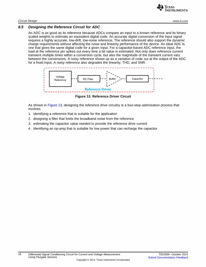
8.5 Designing the Reference Circuit for ADCAn ADC is as good as its reference because ADCs compare an input to a known reference and its binaryscaled weights to estimate an equivalent digital code. An accurate digital conversion of the input signalrequires a highly accurate, low-drift, low-noise reference. The reference should also support the dynamiccharge requirements without affecting the noise and linearity performance of the device. An ideal ADC isone that gives the same digital code for a given input. For a capacitor-based ADC reference input, theload at the reference pin spikes out every time a bit value is estimated. Not only does reference currenttransient multiple times within a conversion cycle, but also the magnitude of the transient current varybetween the conversions. A noisy reference shows up as a variation of code out at the output of the ADCfor a fixed input. A noisy reference also degrades the linearity, THD, and SNR.
Figure 13. Reference Driver Circuit
As shown in Figure 13, designing the reference drive circuitry is a four-step optimization process thatinvolves1. identifying a reference that is suitable for the application2. designing a filter that limits the broadband noise from the reference3. estimating the capacitor value needed to provide the reference drive current4. identifying an op-amp that is suitable for low power that can recharge the capacitor
18 Differential Signal Conditioning Circuit for Current and Voltage Measurement TIDU569–October 2014Using Fluxgate Sensors Submit Documentation Feedback
Copyright © 2014, Texas Instruments Incorporated

0
1000
2000
3000
4000
5000
6000
7000
8000
1 10 100 1000
nV
/H
z√
Iq_ref (uA)
Approximation of Broadband Noise Density
for Bandgap References
( )Broadband _Noise _Density
A10,000 nVREF
Hz 2 IQ _REF in A
m= ´
´ m
www.ti.com Circuit Design
There are two types of noise that a reference can introduce: flicker noise and broadband noise. Flickernoise is the noise dominant at low frequencies and broadband noise dominates at high frequencies. Thebroadband noise, in particular, can be of the order of hundreds of microvolts and can easily exceed thetens of microvolts of RMS noise of the converter. Typically, flicker noise is specified on the datasheet aspeak-to-peak noise up to 10 Hz. This noise has to be scaled down by a factor of 6.6 to convert it into RMSnoise. On the other hand, the density of broadband spectral noise may not be specified on the datasheet.For a band-gap reference, the density is 0.1 μVRMS/√Hz to 10 μVRMS/√Hz in magnitude and is inverselyproportional to the square root of the quiescent current of the reference. If the reference is not specified,Equation 4 gives a good approximation:
(4)
As seen from Figure 14, noise and power are inversely related. A reference with low IQ inherently comeswith higher noise.
Figure 14. Broadband Noise versus Reference Quiescent Current
For REF5025, IQ_REF = 800 μA, which gives the broadband noise a density equal to 250 nV/√Hz usingFigure 14.
19TIDU569–October 2014 Differential Signal Conditioning Circuit for Current and Voltage MeasurementUsing Fluxgate SensorsSubmit Documentation Feedback
Copyright © 2014, Texas Instruments Incorporated

DNC1
VIN2
TEMP3
GND4
TRIM/NR5
VOUT6
NC7
DNC8
U14
REF5025AID
1µFC21
AVDD
GND GND
1µF
C22
1.00kR34
GND
GND
GND
AVDD
0
R35
0
R36 VREF_BUFVREF_BUF
0
R37DNP
0
R331
2
3
4
5
U15
OPA322AIDBVR
0.1µF
C25
GND
10µFC23
0.1µFC24DNP
Circuit Design www.ti.com
BufferAn op-amp is needed to recharge the capacitor above. Additional noise introduced by the buffer should beminimized while selecting this op-amp. However, this selection is less of a concern because unlikereferences where output noise density is a few μV/√Hz, the same will be in the range of10 nV/√Hz to 100 nV/√Hz for op-amps. The broadband noise gets further band-limited by the isolationresistor and the capacitor following the buffer. Flicker and broadband noise introduced by the op-ampshould be verified for it to be significantly smaller (less than one-third) than the reference noise beforefinalizing on the op-amp. Reducing the buffer noise to less than a third of the reference noise makes theop-amp noise term insignificant when it gets added to the reference noise (square root of summation ofsquares). Flicker noise is specified on the datasheet as peak-to-peak noise up to 10 Hz. This noise has tobe scaled down by a factor of 6.6 to convert it into RMS noise. The total noise introduced by the op-amp isthe square root of the sum of the squares of the flicker noise and broadband RMS noise. Equation 3 canbe used to verify the same.
Note that high resolution converters cause the size of the capacitor in the charge bucket to become toolarge, causing stability issues in most of the op-amps. This issue can be addressed with a series isolationresistor at the cost of the bandwidth of the op-amp. Choosing the right capacitor, op-amp, and isolationresistor is an iterative process that has to be verified by simulation. During this process the capacitancemight require minimal adjustments from the starting value taking stability, voltage drop, and cutofffrequency into consideration.
Reference for External ADC: REF5025 + OPA322The REF5025 is used as a 2.5-V voltage reference device. Use a supply bypass capacitor rangingbetween 1 to 10 μF. The REF5025 allows access to the band-gap through the TRIM/NR pin. Placing acapacitor from the TRIM/NR pin to GND in combination with the internal resistors creates a low-pass filter.A capacitance of 1 μF creates a low-pass filter with the corner frequency between 10 and 20 Hz. This filterdecreases the overall noise measured on the VOUT pin by half. A higher capacitance results in a lower filtercutoff frequency, further reducing output noise. Note that use of this capacitor increases startup time.Figure 15 shows schematic capture of REF5025 and the OPA322-based buffer connected at the output ofthe REF5025 so as to recharge the capacitor at the output.
Figure 15. REF5025 + OPA322 Circuit
20 Differential Signal Conditioning Circuit for Current and Voltage Measurement TIDU569–October 2014Using Fluxgate Sensors Submit Documentation Feedback
Copyright © 2014, Texas Instruments Incorporated

IN1
2
EN3
NC4
OUT5
GND
U10
TLV70033DCKR
1µFC8
GND
1µFC2
GND
GND
AVDD 3V3
D1
MBRA160T3G
GND
AVDD
1
3
2
J5
PJ-102A
GND
6-V Input 5-V Output1
2
J6
1751248
OUT1
NC2
SENSE3
6P4V24
6P4V15
3P2V6
GND7
1P6V8
0P8V9
0P4V10
0P2V11
0P1V12
EN13
NR14
IN15
IN16
NC17
NC18
NC19
OUT20
PAD21
U5
TPS7A4700RGW
10µFC4
10µFC9
10µFC3
10µFC13
GND
1µFC53
GNDGND
10µFC1
GND
Green
A2
C1
LD1
GND
0R1
0R145
1.00kR20
AVDD
GND
1µFC14
GND
REF2025_REF/2
REF2025_REF
GND GND
0R26
0R21
0.1µFC20
0.1µFC15
VBIAS1
GND2
EN3
VIN4
VREF5
U13
REF2025DBV
REF2025_REF
REF2025_REF/2
www.ti.com Circuit Design
Reference for Internal ADC of Delfino F2837x: REF2025The REF2025 can provide two reference voltages, 1.25 V and 2.5 V. The 2.5 V is given as reference tothe integrated ADC, and 1.25 V is used as output common-mode voltage for the THS4531. Figure 16shows the reference circuit using the REF2025.
Figure 16. REF2025 Circuit to Provide 1.25 V and 2.5 V as Reference
8.6 Power Supply: 5-V and 3.3-V GenerationThe TIDA-00201 board can be powered through connector J6. The input voltage can be 6 V, 15 V, or24 V based on the availability in the industrial drive. The output voltage for the TPS7A4700 is set bygrounding the appropriate control pins. When grounded, all control pins add a specific voltage on top ofthe internal reference voltage (VREF = 1.4 V). For example, when grounding pins 0P4V and 3P2V, thevoltage values 0.4 V and 3.2 V are added to the 1.4-V internal reference voltage for VOUT(NOM) equal to 5.0V. Figure 17 shows the TPS7A4700 section of the design. One green LED (LD1) is provided to indicateavailability of the 5-V output.
Figure 17. 6-V to 5-V Conversion Using TPS7A4700
TLV70033 converts the 5 V to 3.3 V. Figure 18 shows the schematic for the same.
Figure 18. 5-V to 3.3-V Conversion Using TLV70033
21TIDU569–October 2014 Differential Signal Conditioning Circuit for Current and Voltage MeasurementUsing Fluxgate SensorsSubmit Documentation Feedback
Copyright © 2014, Texas Instruments Incorporated

OC_FAULTOC_FAULT
3V3
Green
A2
C1
LD3
10kR45
3
2
1
84
U7ATLC372
5
6
7
U7BTLC372
GND
AVDD
GND
0.1µF
C7
GNDOUT3
AVDD
3.30kR5
3.30kR7
20.0kR6
Circuit Design www.ti.com
8.7 Design for Overcurrent and Earth Fault Detection CircuitsGenerally, the fluxgate sensors can be operated up to 300% of their nominal current ratings for a shorterduration. If the current goes beyond 300%, enable the protection mechanism. For example, in this design,the thresholds are calculated as follows:• Nominal current rating (In) = 6 Amperes
Corresponding fluxgate sensor output voltage = 0.625 Volts• 300% of the nominal rating = 18 Amperes
Corresponding fluxgate sensor output voltage at 300% current = 0.625 × 3 = 1.875 Volts
The output of fluxgate sensor always rides on 2.5 V, so the positive and negative values can go up to4.375 V and 0.625 V, respectively. Considering 50 mV as a buffer, the thresholds are calculated as:• Threshold for positive cycle = VTH (pos) = 2.5 V + 1.875 V + 0.05 V = 4.38 Volts• Threshold for negative cycle = VTH (neg) = 2.5 V – 1.875 V – 0.05 V = 0.62 Volts
8.7.1 Overcurrent ProtectionThe overcurrent protection is implemented as shown in Figure 19. The resistor dividers are calculated forVTH (pos) = 4.38 V and VTH (neg) = 0.62 V. Each channel has individual overcurrent protection. Theindication of the overcurrent's condition is shown with an LED at the output.
Figure 19. Overcurrent Protection Using TLC372
22 Differential Signal Conditioning Circuit for Current and Voltage Measurement TIDU569–October 2014Using Fluxgate Sensors Submit Documentation Feedback
Copyright © 2014, Texas Instruments Incorporated
GND_FAULTOC_FAULT 1
2
J17
282834-2
GND_FAULT
OC_FAULT
3V3
Green
A2
C1
LD2
10kR44
1.0k
R112
1.0k
R111
OUT1
OUT2
OUT3
OUT1
OUT2
OUT31.0k
R110
GND_FAULT
3
2
1
84
U16ATLC372
5
6
7
U16BTLC372
GND
AVDD
GND
0.1µF
C32
GND
AVDD
3.30kR91
3.30kR93
20.0kR92
www.ti.com Circuit Design
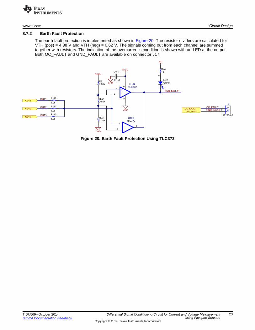
8.7.2 Earth Fault ProtectionThe earth fault protection is implemented as shown in Figure 20. The resistor dividers are calculated forVTH (pos) = 4.38 V and VTH (neg) = 0.62 V. The signals coming out from each channel are summedtogether with resistors. The indication of the overcurrent's condition is shown with an LED at the output.Both OC_FAULT and GND_FAULT are available on connector J17.
Figure 20. Earth Fault Protection Using TLC372
23TIDU569–October 2014 Differential Signal Conditioning Circuit for Current and Voltage MeasurementUsing Fluxgate SensorsSubmit Documentation Feedback
Copyright © 2014, Texas Instruments Incorporated
1
2
3
4
5
6
7
8
J19
HEADER_1X8
SCLK
CS
GND
SDO_B_1
SDO_A_1
SDO_B_2
SDO_A_2
SCLK
SDISDI
SDO_A_1
SDO_A_2
SDO_B_1
SDO_B_2
CS
AINP_A
10µFC19
10µFC16
GND
AINP_B
0R15
10µFC12
GND
47R17
47R23
47R82
47R81
47R31
0R28
10µFC30
GND
100kR32
DNP
GND
AVDD
3V3
AINP_A1
AINM_A2
REFIO_A3
REFGND_A4
REFGND_B5
REFIO_B6
AINM_B7
AINP_B8
DVDD9
SDI10
CS11
SCLK12
AVDD16
GND15
SDO_B14
SDO_A13
U12
ADS7854
0.22R24
0.22R19
AINM_A
AINM_B SDI
CS
SCLK
SDO_A_1
SDO_B_1
AINP_A
AINM_A
AINM_B
AINP_B
AINP_C
10µFC17
10µFC18
GND
AINP_D
0R14
10µFC11
GND
47R16
47R22
0R27
10µFC31
GND
AVDD
3V3
AINP_A1
AINM_A2
REFIO_A3
REFGND_A4
REFGND_B5
REFIO_B6
AINM_B7
AINP_B8
DVDD9
SDI10
CS11
SCLK12
AVDD16
GND15
SDO_B14
SDO_A13
U11
ADS7854
0.22R18
0.22R25
AINM_C
AINM_D SDI 1
CS 1
SCLK1
SDO_A_2
SDO_B_2
AINP_C
AINM_C
AINM_D
AINP_D
VREF_BUFVREF_BUF
VREF_BUFVREF_BUF
VREF_BUFVREF_BUF
VREF_BUFVREF_BUF
SCLK1
CS 1
SDI 1
0R30
0R29
0R80
0R150DNP
0R151DNP
0R152DNP
0R153DNP
Circuit Design www.ti.com
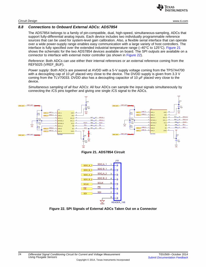
8.8 Connections to Onboard External ADCs: ADS7854The ADS7854 belongs to a family of pin-compatible, dual, high-speed, simultaneous-sampling, ADCs thatsupport fully-differential analog inputs. Each device includes two individually programmable referencesources that can be used for system-level gain calibration. Also, a flexible serial interface that can operateover a wide power-supply range enables easy communication with a large variety of host controllers. Theinterface is fully specified over the extended industrial temperature range (–40°C to 125°C). Figure 21shows the schematic for the two ADS7854 devices available on board. The SPI outputs are available on aconnector to interface with external motor controller (as shown in Figure 22).
Reference: Both ADCs can use either their internal references or an external reference coming from theREF5025 (VREF_BUF).
Power supply: Both ADCs are powered at AVDD with a 5-V supply voltage coming from the TPS7A4700with a decoupling cap of 10 μF placed very close to the device. The DVDD supply is given from 3.3 Vcoming from the TLV70033. DVDD also has a decoupling capacitor of 10 μF placed very close to thedevice.
Simultaneous sampling of all four ADCs: All four ADCs can sample the input signals simultaneously byconnecting the /CS pins together and giving one single /CS signal to the ADCs.
Figure 21. ADS7854 Circuit
Figure 22. SPI Signals of External ADCs Taken Out on a Connector
24 Differential Signal Conditioning Circuit for Current and Voltage Measurement TIDU569–October 2014Using Fluxgate Sensors Submit Documentation Feedback
Copyright © 2014, Texas Instruments Incorporated
www.ti.com Circuit Design
8.9 Connections to Delfino F2837x Control CardThe Delfino F28377D Control Card (TMDSCNCD28377D) from TI provides a great way to learn andexperiment with the F2837x device family within TI’s C2000™ family of microcontrollers (MCUs). This180-pin control card is intended to provide a well-filtered robust design capable of working in mostindustrial environments.
The F28377D Control Card features:• Delfino F28377D MCU: A high performance C2000 MCU• 180-pin HSEC8 edge card interface: Allows for compatibility with all of C2000’s 180-pin control card
application kits and control cards. Compatibility with 100-pin control cards can be accomplished usingthe TMDSADAP180TO100 adapter card (sold separately)
• Built-in isolated JTAG emulation: An XDS100v2 emulator that provides a convenient interface to CodeComposer Studio (CCS) without additional hardware. Flipping a switch allows an external JTAGemulator to be used
• Connectivity: Contains connectors that allow the user to experiment with USB, a microSD card, andisolated UART/SCI with the F2837x MCU
• Key signal breakout: Most GPIOs, ADCs, and other key signals routed to hard gold connector fingers• Robust power supply filtering: A single 5-V input supply that powers an on-CARD 3.3-V LDO. All MCU
inputs are then decoupled using LC filters near the device• ADC clamping: ADC inputs clamped by protection diodes
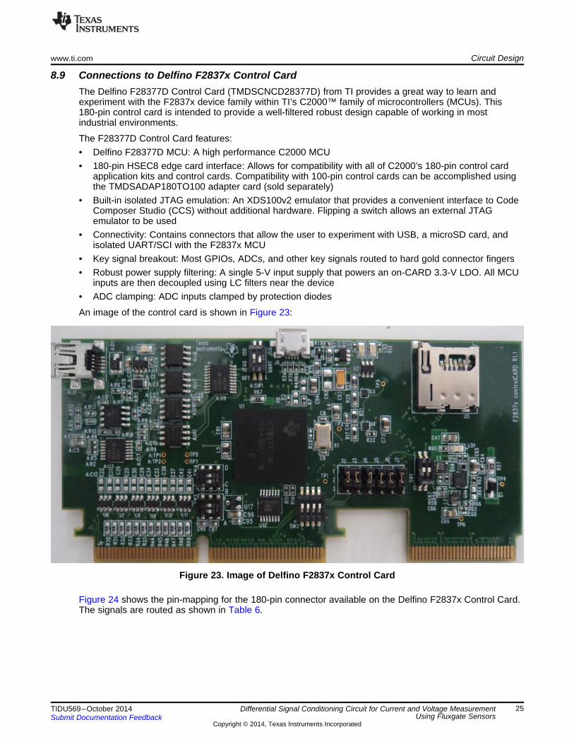
An image of the control card is shown in Figure 23:
Figure 23. Image of Delfino F2837x Control Card
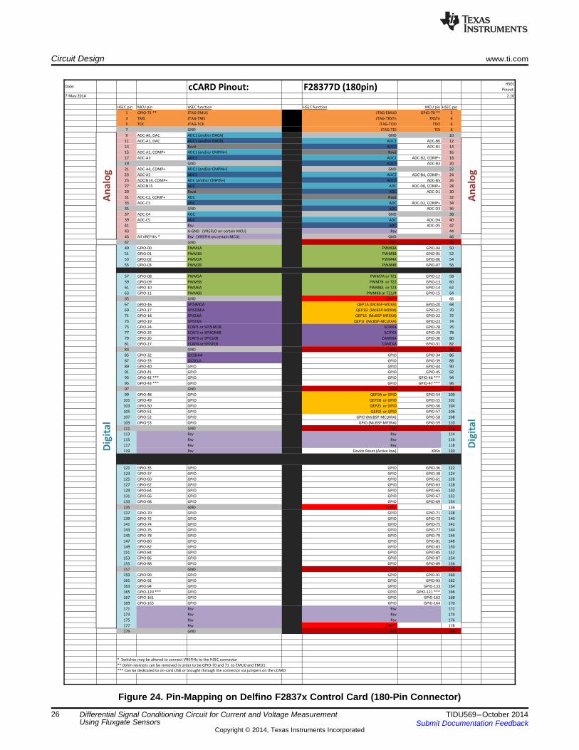
Figure 24 shows the pin-mapping for the 180-pin connector available on the Delfino F2837x Control Card.The signals are routed as shown in Table 6.
25TIDU569–October 2014 Differential Signal Conditioning Circuit for Current and Voltage MeasurementUsing Fluxgate SensorsSubmit Documentation Feedback
Copyright © 2014, Texas Instruments Incorporated
Date: cCARD Pinout: F28377D (180pin)HSEC
Pinout:
7-May-2014 2.10
HSEC pin MCU pin HSEC function HSEC function MCU pin HSEC pin
1 GPIO-71 ** JTAG-EMU1 JTAG-EMU0 GPIO-70 ** 2
3 TMS JTAG-TMS JTAG-TRSTn TRSTn 4
5 TCK JTAG-TCK JTAG-TDO TDO 6
7 GND JTAG-TDI TDI 8
9 ADC-A0, DAC ADC1 (and/or DACA) GND 10
11 ADC-A1, DAC ADC1 (and/or DACB) ADC2 ADC-B0 12
13 Rsvd ADC2 ADC-B1 14
15 ADC-A2, COMP+ ADC1 (and/or CMPIN+) Rsvd 16
17 ADC-A3 ADC1 ADC2 ADC-B2, COMP+ 18
19 GND ADC2 ADC-B3 20
21 ADC-A4, COMP+ ADC1 (and/or CMPIN+) GND 22
23 ADC-A5 ADC1 ADC2 ADC-B4, COMP+ 24
25 ADCIN14, COMP+ ADC (and/or CMPIN+) ADC2 ADC-B5 26
27 ADCIN15 ADC ADC ADC-D0, COMP+ 28
29 Rsvd ADC ADC-D1 30
31 ADC-C2, COMP+ ADC Rsvd 32
33 ADC-C3 ADC ADC ADC-D2, COMP+ 34
35 GND ADC ADC-D3 36
37 ADC-C4 ADC GND 38
39 ADC-C5 ADC ADC ADC-D4 40
41 Rsv ADC ADC-D5 42
43 A-GND (VREFLO on certain MCU) Rsv 44
45 All VREFHIs * Rsv (VREFHI on certain MCU) GND 46
47 GND 5V0 48
49 GPIO-00 PWM1A PWM3A GPIO-04 50
51 GPIO-01 PWM1B PWM3B GPIO-05 52
53 GPIO-02 PWM2A PWM4A GPIO-06 54
55 GPIO-03 PWM2B PWM4B GPIO-07 56
57 GPIO-08 PWM5A PWM7A or TZ1 GPIO-12 58
59 GPIO-09 PWM5B PWM7B or TZ2 GPIO-13 60
61 GPIO-10 PWM6A PWM8A or TZ3 GPIO-14 62
63 GPIO-11 PWM6B PWM8B or TZ1/4 GPIO-15 64
65 GND 12V0? 66
67 GPIO-16 SPISIMOA QEP1A (McBSP-MDXA) GPIO-20 68
69 GPIO-17 SPISOMIA QEP1B (McBSP-MDRA) GPIO-21 70
71 GPIO-18 SPICLKA QEP1S (McBSP-MFSXA) GPIO-22 72
73 GPIO-19 SPISTEA QEP1I (McBSP-MCLKXA) GPIO-23 74
75 GPIO-24 ECAP1 or SPISIMOB SCIRXA GPIO-28 76
77 GPIO-25 ECAP2 or SPISOMIB SCITXA GPIO-29 78
79 GPIO-26 ECAP3 or SPICLKB CANRXA GPIO-30 80
81 GPIO-27 ECAP4 or SPISTEB CANTXA GPIO-31 82
83 GND 5V0 84
85 GPIO-32 I2CSDAA GPIO GPIO-34 86
87 GPIO-33 I2CSCLA GPIO GPIO-39 88
89 GPIO-40 GPIO GPIO GPIO-44 90
91 GPIO-41 GPIO GPIO GPIO-45 92
93 GPIO-42 *** GPIO GPIO GPIO-46 *** 94
95 GPIO-43 *** GPIO GPIO GPIO-47 *** 96
97 GND 5V0 98
99 GPIO-48 GPIO QEP2A or GPIO GPIO-54 100
101 GPIO-49 GPIO QEP2B or GPIO GPIO-55 102
103 GPIO-50 GPIO QEP2S or GPIO GPIO-56 104
105 GPIO-51 GPIO QEP2I or GPIO GPIO-57 106
107 GPIO-52 GPIO GPIO (McBSP-MCLKRA) GPIO-58 108
109 GPIO-53 GPIO GPIO (McBSP-MFSRA) GPIO-59 110
111 GND 5V0 112
113 Rsv Rsv 114
115 Rsv Rsv 116
117 Rsv Rsv 118
119 Rsv Device Reset (Active low) XRSn 120
121 GPIO-35 GPIO GPIO GPIO-36 122
123 GPIO-37 GPIO GPIO GPIO-38 124
125 GPIO-60 GPIO GPIO GPIO-61 126
127 GPIO-62 GPIO GPIO GPIO-63 128
129 GPIO-64 GPIO GPIO GPIO-65 130
131 GPIO-66 GPIO GPIO GPIO-67 132
133 GPIO-68 GPIO GPIO GPIO-69 134
135 GND 12V0? 136
137 GPIO-70 GPIO GPIO GPIO-71 138
139 GPIO-72 GPIO GPIO GPIO-73 140
141 GPIO-74 GPIO GPIO GPIO-75 142
143 GPIO-76 GPIO GPIO GPIO-77 144
145 GPIO-78 GPIO GPIO GPIO-79 146
147 GPIO-80 GPIO GPIO GPIO-81 148
149 GPIO-82 GPIO GPIO GPIO-83 150
151 GPIO-84 GPIO GPIO GPIO-85 152
153 GPIO-86 GPIO GPIO GPIO-87 154
155 GPIO-88 GPIO GPIO GPIO-89 156
157 GND 5V0 158
159 GPIO-90 GPIO GPIO GPIO-91 160
161 GPIO-92 GPIO GPIO GPIO-93 162
163 GPIO-94 GPIO GPIO GPIO-133 164
165 GPIO-120 *** GPIO GPIO GPIO-121 *** 166
167 GPIO-161 GPIO GPIO GPIO-162 168
169 GPIO-163 GPIO GPIO GPIO-164 170
171 Rsv Rsv 172
173 Rsv Rsv 174
175 Rsv Rsv 176
177 Rsv 12V0? 178
179 GND 5V0 180
* Switches may be altered to connect VREFHIs to the HSEC connector
** 0ohm resistors can be removed in order to tie GPIO-70 and 71 to EMU0 and EMU1
*** Can be dedicated to on-card USB or brought through the connector via jumpers on the cCARD
An
alo
g
An
alo
gD
igit
al
Dig
ita
l
Circuit Design www.ti.com
Figure 24. Pin-Mapping on Delfino F2837x Control Card (180-Pin Connector)
26 Differential Signal Conditioning Circuit for Current and Voltage Measurement TIDU569–October 2014Using Fluxgate Sensors Submit Documentation Feedback
Copyright © 2014, Texas Instruments Incorporated

1 2
3 4
5 6
7 8
9 10
11 12
13 14
15 16
17 18
19 20
21 22
23 24
25 26
27 28
29 30
31 32
33 34
35 36
37 38
39 40
41 42
43 44
45 46
47 48
49 50
51 52
53 54
55 56
57 58
59 60
J16A
SPD08-120-L-RB
61 62
63 64
65 66
67 68
69 70
71 72
73 74
75 76
77 78
79 80
81 82
83 84
85 86
87 88
89 90
91 92
93 94
95 96
97 98
99 100
101 102
103 104
105 106
107 108
109 110
111 112
113 114
115 116
117 118
119 120
J16B
SPD08-120-L-RB121
123
125
127
129
131
133
135
137
139
141
143
145
147
149
151
153
155
157
159
161
163
165
167
169
171
173
175
177
179
122
124
126
128
130
132
134
136
138
140
142
144
146
148
150
152
154
156
158
160
162
164
166
168
170
172
174
176
178
180
J15SPD08-060-RB-TR
0R560R55
DNPSDO_B_2SDO_A_2
0R63SDI
0R40SCLK
0R41SCLK
0R59CS
0R54
0R47
AVDD
AVDD
GND
0R42
SCLK
SDI
SDO_A_2
SDO_B_2
CS
0R58REF2025_REF/2
0R57REF2025_REFREF2025_REF
REF2025_REF/2
AIN2MAIN2M
AIN2PAIN2P
0R52
0R53
AIN3P
AIN3MAIN3M
AIN3P0R48
0R49
AIN4P
AIN4MAIN4M
AIN4P0R60
0R61
0R43
GND
3.6VD3
3.6VD4
3.6VD8
3.6VD7
3.6VD5
3.6VD9
GND
GND
1µFC58
1µFC59
GND
GND
AIN1M
AIN1P
0R51
0R50AIN1P
AIN1M
3.6VD2
3.6VD6
GND
0R154
0R155
0R156
0R157
0R158
0R159
0R160
0R161
GND
GND
GND
GND
GND
GND
GND
GND
0R62SDI
SDO_B_1SDO_A_1
0R38DNP
0R39SDO_A_1
SDO_B_1
www.ti.com Circuit Design
Table 6. Pin-Mapping Details
MAPPING ON TIDA-00201 BOARDPIN NUMBER ON CONTROL CARD PIN FUNCTIONALITY (J15 AND J16)7, 10, 19, 22, 35, 46, 97, 111, 160, 161 GND GND
15 ADC-A2, COMP+ AIN2P17 ADC-A3 AIN2M18 ADC-B2, COMP+ AIN1M20 ADC-B3 AIN1P21 ADC-A4, COMP+ AIN3P23 ADC-A5 AIN3M25 ADCIN14, COMP+ AIN4P27 ADCIN15 AIN4M39 ADC-C5 REF2025 REF/245 All VREFHIs REF2025 REF
67, 77 SPISIMOA, SPISOMIB SDI for onboard ADS785469, 75 SPISOMIA, SPISIMOB SDOA and SDOB from onboard ADS785471, 79 SPICLKA SCLK for onboard ADS7854
89 GPIO /CS for onboard ADS7854112, 180 AVDD AVDD (5 V)
Figure 25 shows the schematic capture for the pin-mapping explained in Table 6. Although the controlcard has clamping diodes at each of the analog inputs, this design provides an option to mount externalclamping diodes as well.
Figure 25. Schematic Capture for J15 and J16 (to Connect to 180-Pin Connector on Control Card)
27TIDU569–October 2014 Differential Signal Conditioning Circuit for Current and Voltage MeasurementUsing Fluxgate SensorsSubmit Documentation Feedback
Copyright © 2014, Texas Instruments Incorporated

Test Setup and Test Results www.ti.com
9 Test Setup and Test Results
9.1 Noise Filtering for Fluxgate Current SensorAs explained in Section 8.4, low-pass filters are used to filter out the 450-kHz / 900-kHz noise signal fromfluxgate sensors. Figure 26 shows the waveforms before and after the filter. The noise signal on OUT pinof the fluxgate sensor is having frequency of 452.1 kHz, which is same as the internal fluxgate oscillatorfrequency.
NOTE: The signals captured in Figure 26 also include noise from the oscilloscope itself.
Figure 26. Noise Signal Before and After the Low-Pass Filter
9.2 DC (or Dynamic) Performance of the System Using External ADC ADS7254All ADC circuits suffer from some amount of inherent broadband noise contributed by the internalresistors, capacitors, and other circuitry, which is referred to the inputs of the ADC. The front-end drivercircuit also contributes some noise to the system, which can also be referred to the ADC inputs. Thecumulative noise, often called as the input-referred noise of the ADC, has a significant impact on theoverall system performance. The most common way to characterize this noise is by using a constant DCvoltage as the input signal and collecting a large number of ADC output codes. A histogram can then beplotted to show the distribution of output codes, which can be used to illustrate the impact of noise on theoverall system performance. For a theoretically perfect ADC system, the histogram of output codes is asingle vertical bar because the ADC output is always the same for a DC input voltage. However, the noisecontributions from the ADC and the front-end circuit lead to a distribution of output codes, which providesa measure of the overall system's DC noise. If the output code distribution has large peaks and valleysthat make it distinctly non- Gaussian, then the histogram indicates significant DNL errors in the ADC orissues with the system design such as insufficient power supply decoupling, improper ground connections,or other poor PCB layout effects.
The noise-free resolution of an ADC is defined as the number of steady output bits from the converterbeyond. The system performance is dominated by noise, and it is not possible to differentiate betweenindividual code transitions. This resolution is an extremely conservative measurement of the ADC'sperformance because the formula for noise-free resolution is derived from the peak-to-peak code noise,which is extremely dependent on the total number of samples. Do not confuse the effective noise-freeresolution and effective number of bits (ENOB) with each other as they are two completely differententities. The ENOB for an ADC is measured with an AC sinusoidal input signal and includes the effectsdue to quantization noise and distortion terms, which have no impact on a DC measurement.
28 Differential Signal Conditioning Circuit for Current and Voltage Measurement TIDU569–October 2014Using Fluxgate Sensors Submit Documentation Feedback
Copyright © 2014, Texas Instruments Incorporated
www.ti.com Test Setup and Test Results
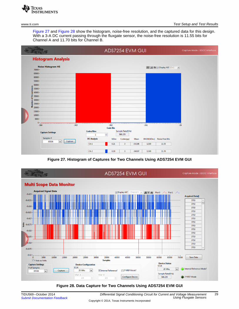
Figure 27 and Figure 28 show the histogram, noise-free resolution, and the captured data for this design.With a 3-A DC current passing through the fluxgate sensor, the noise-free resolution is 11.55 bits forChannel A and 11.70 bits for Channel B.
Figure 27. Histogram of Captures for Two Channels Using ADS7254 EVM GUI
Figure 28. Data Capture for Two Channels Using ADS7254 EVM GUI
29TIDU569–October 2014 Differential Signal Conditioning Circuit for Current and Voltage MeasurementUsing Fluxgate SensorsSubmit Documentation Feedback
Copyright © 2014, Texas Instruments Incorporated
SNR 6.02 N 1.76
– 1SNRN
6.02
.76
= ´ +
=
2 2n _ TOT _RMS n _ AMP _RMS n _ ADC _RMS
SIG _RMSSYS
n _ TOT _RMS
V V V
VSNR
V
= +
=
0
-10
-20
-30
-40
-50
-60
-70
-80
-90
-100
-110
-120
-1300 1k 2k 3k 4k 5k 6k 7k 8k 9k 10k
Frequency (Hz)
Am
plitu
de
(dB
)Digitized Signal Power
Noise
Harmonics
SNR =Digitized Signal Power
Noise
SINAD =Digitized Signal Power
Noise + Harmonic Power
Digitized Signal Power
Harmonic PowerTHD =
Test Setup and Test Results www.ti.com
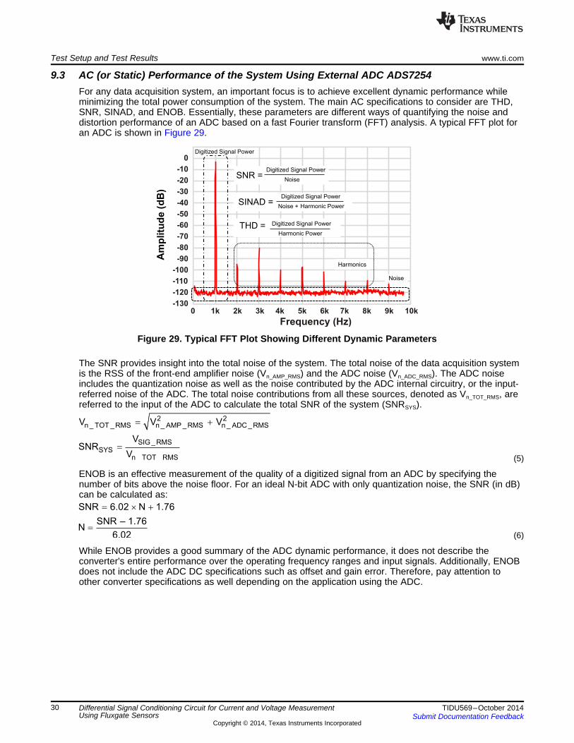
9.3 AC (or Static) Performance of the System Using External ADC ADS7254For any data acquisition system, an important focus is to achieve excellent dynamic performance whileminimizing the total power consumption of the system. The main AC specifications to consider are THD,SNR, SINAD, and ENOB. Essentially, these parameters are different ways of quantifying the noise anddistortion performance of an ADC based on a fast Fourier transform (FFT) analysis. A typical FFT plot foran ADC is shown in Figure 29.
Figure 29. Typical FFT Plot Showing Different Dynamic Parameters
The SNR provides insight into the total noise of the system. The total noise of the data acquisition systemis the RSS of the front-end amplifier noise (Vn_AMP_RMS) and the ADC noise (Vn_ADC_RMS). The ADC noiseincludes the quantization noise as well as the noise contributed by the ADC internal circuitry, or the input-referred noise of the ADC. The total noise contributions from all these sources, denoted as Vn_TOT_RMS, arereferred to the input of the ADC to calculate the total SNR of the system (SNRSYS).
(5)
ENOB is an effective measurement of the quality of a digitized signal from an ADC by specifying thenumber of bits above the noise floor. For an ideal N-bit ADC with only quantization noise, the SNR (in dB)can be calculated as:
(6)
While ENOB provides a good summary of the ADC dynamic performance, it does not describe theconverter's entire performance over the operating frequency ranges and input signals. Additionally, ENOBdoes not include the ADC DC specifications such as offset and gain error. Therefore, pay attention toother converter specifications as well depending on the application using the ADC.
30 Differential Signal Conditioning Circuit for Current and Voltage Measurement TIDU569–October 2014Using Fluxgate Sensors Submit Documentation Feedback
Copyright © 2014, Texas Instruments Incorporated
www.ti.com Test Setup and Test Results
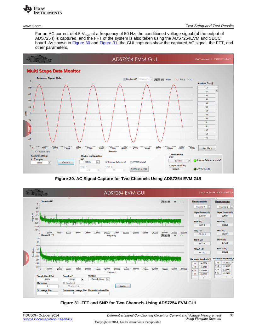
For an AC current of 4.5 VRMS at a frequency of 50 Hz, the conditioned voltage signal (at the output ofADS7254) is captured, and the FFT of the system is also taken using the ADS7254EVM and SDCCboard. As shown in Figure 30 and Figure 31, the GUI captures show the captured AC signal, the FFT, andother parameters.
Figure 30. AC Signal Capture for Two Channels Using ADS7254 EVM GUI
Figure 31. FFT and SNR for Two Channels Using ADS7254 EVM GUI
31TIDU569–October 2014 Differential Signal Conditioning Circuit for Current and Voltage MeasurementUsing Fluxgate SensorsSubmit Documentation Feedback
Copyright © 2014, Texas Instruments Incorporated

Test Setup and Test Results www.ti.com
The FFT for both channels show an SNR of approximately 65 dB at a signal amplitude of –9 dBFS. Thisresult is just an indication of performance, but the actual SNR can be measured when the device isoperated with an input voltage that has reached the full-scale value of the ADC input range. Figure 32 isthe setup used to measure the AC and DC performance for this reference design.
Figure 32. Test Setup for AC and DC Tests for ADS7254
32 Differential Signal Conditioning Circuit for Current and Voltage Measurement TIDU569–October 2014Using Fluxgate Sensors Submit Documentation Feedback
Copyright © 2014, Texas Instruments Incorporated

Primary Current (A)
Accu
racy (
%)
-1 -1.5 -2 -2.5 -3 -3.5 -4 -4.5 -5 -5.5 -6-0.5
-0.4
-0.3
-0.2
-0.1
0
0.1
0.2
0.3
0.4
0.5
D004b
FDA Accuracy at 75C (-Ve Current)
Primary Current (A)
Accu
racy (
%)
1 1.5 2 2.5 3 3.5 4 4.5 5 5.5 6-0.5
-0.4
-0.3
-0.2
-0.1
0
0.1
0.2
0.3
0.4
0.5
D004a
FDA Accuracy at 75C (+Ve Current)
Primary Current (A)
Accura
cy (
%)
-1 -1.5 -2 -2.5 -3 -3.5 -4 -4.5 -5 -5.5 -6-0.5
-0.4
-0.3
-0.2
-0.1
0
0.1
0.2
0.3
0.4
0.5
D001b
FDA Accuracy at 25C (-Ve Current)
Primary Current (A)
Accura
cy (
%)
1 1.5 2 2.5 3 3.5 4 4.5 5 5.5 6-0.5
-0.4
-0.3
-0.2
-0.1
0
0.1
0.2
0.3
0.4
0.5
D001a
FDA Accuracy at 25C (+Ve Current)
www.ti.com Test Setup and Test Results
9.4 DC Accuracy Tests (at 25°C and 75°C)The following figures show the accuracy of the signal at each stage. Figure 33 shows accuracy of signal atthe output of THS4531 at 25°C, and Figure 34 shows accuracy of signal at 75°C. The graphs include theoffset and gain error compensation along with passive component mismatches in the feedback path of theTHS4531.
Figure 33. FDA Accuracy at 25°C for Positive Current (Left) for Negative Current (Right)
Figure 34. FDA Accuracy at 75°C for Positive Current (Left) for Negative Current (Right)
33TIDU569–October 2014 Differential Signal Conditioning Circuit for Current and Voltage MeasurementUsing Fluxgate SensorsSubmit Documentation Feedback
Copyright © 2014, Texas Instruments Incorporated

Primary Current (A)
Accu
racy (
%)
-1 -1.5 -2 -2.5 -3 -3.5 -4 -4.5 -5 -5.5 -6-0.5
-0.4
-0.3
-0.2
-0.1
0
0.1
0.2
0.3
0.4
0.5
D005b
ADC Accuracy at 75C (-Ve Current)
Primary Current (A)
Accu
racy (
%)
1 1.5 2 2.5 3 3.5 4 4.5 5 5.5 6-0.5
-0.4
-0.3
-0.2
-0.1
0
0.1
0.2
0.3
0.4
0.5
D005a
ADC Accuracy at 75C (+Ve Current)
Primary Current (A)
Accu
racy (
%)
-1 -1.5 -2 -2.5 -3 -3.5 -4 -4.5 -5 -5.5 -6-0.5
-0.4
-0.3
-0.2
-0.1
0
0.1
0.2
0.3
0.4
0.5
D002b
ADC Accuracy at 25C (-Ve Current)
Primary Current (A)
Accu
racy (
%)
1 1.5 2 2.5 3 3.5 4 4.5 5 5.5 6-0.5
-0.4
-0.3
-0.2
-0.1
0
0.1
0.2
0.3
0.4
0.5
D002a
ADC Accuracy at 25C (+Ve Current)
Test Setup and Test Results www.ti.com
Figure 35 shows accuracy of the signal at the output of the ADS7254 at 25°C, and Figure 36 showsaccuracy of ADC at 75°C. The graphs includes the linearity and gain error from the ADC itself.
Figure 35. ADC Accuracy at 25°C for Positive Current (Left) for Negative Current (Right)
Figure 36. ADC Accuracy at 75°C for Positive Current (Left) for Negative Current (Right)
34 Differential Signal Conditioning Circuit for Current and Voltage Measurement TIDU569–October 2014Using Fluxgate Sensors Submit Documentation Feedback
Copyright © 2014, Texas Instruments Incorporated

Primary Current (A)
Accura
cy (
%)
-1 -1.5 -2 -2.5 -3 -3.5 -4 -4.5 -5 -5.5 -6-0.3
-0.2
-0.1
0
0.1
0.2
0.3
0.4
0.5
0.6
0.7
D006b
Total Accuracy at 75C (-Ve Current)
Primary Current (A)
Accura
cy (
%)
1 1.5 2 2.5 3 3.5 4 4.5 5 5.5 6-0.3
-0.2
-0.1
0
0.1
0.2
0.3
0.4
0.5
0.6
0.7
D006a
Total Accuracy at 75C (+Ve Current)
Primary Current (A)
Accu
racy (
%)
-1 -1.5 -2 -2.5 -3 -3.5 -4 -4.5 -5 -5.5 -6-0.5
-0.4
-0.3
-0.2
-0.1
0
0.1
0.2
0.3
0.4
0.5
D003b
Total Accuracy at 25C (-Ve Current)
Primary Current (A)
Accura
cy (
%)
1 1.5 2 2.5 3 3.5 4 4.5 5 5.5 6-0.5
-0.4
-0.3
-0.2
-0.1
0
0.1
0.2
0.3
0.4
0.5
D003a
Total Accuracy at 25C (+Ve Current)
www.ti.com Test Setup and Test Results
Figure 37 shows accuracy of signal for the entire signal chain (FDA + ADC) at 25°C, and Figure 38 showsthe total accuracy at 75°C. Note that in a typical drive application, the current sensor would be used from30% to 100% of its nominal current rating, so the accuracy should be considered for primary current from±1.75 to ±6 A.
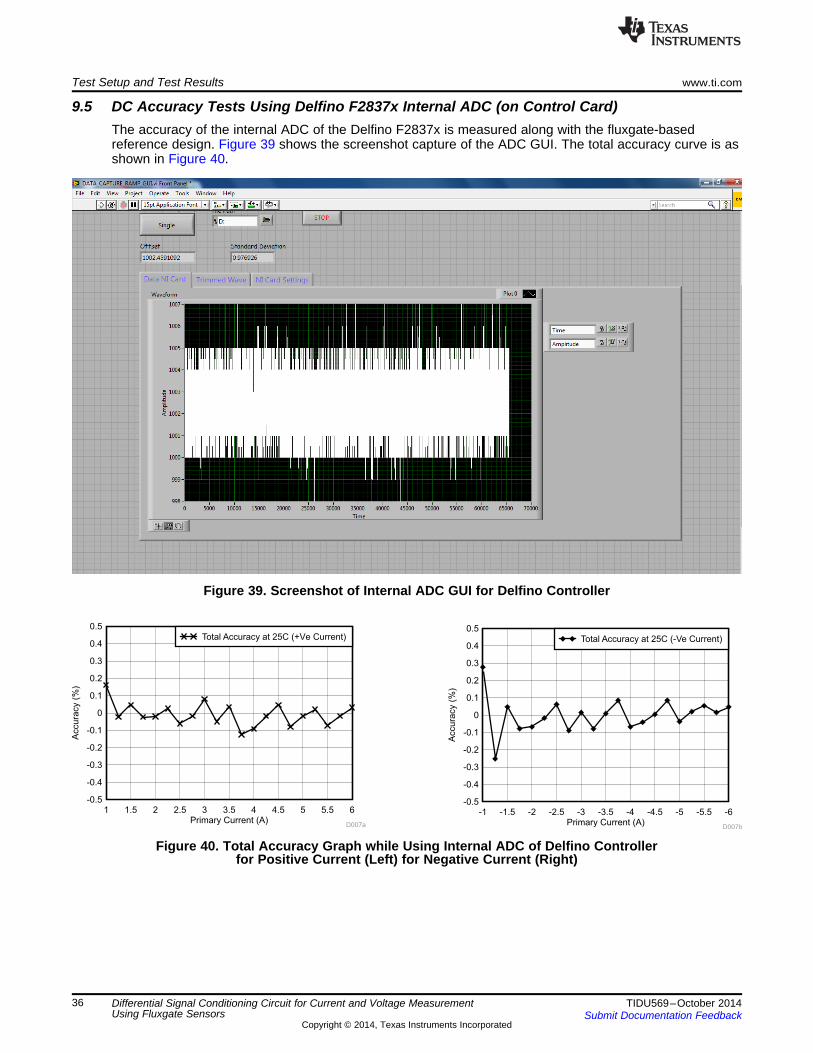
Figure 37. Total Accuracy at 25°C for Positive Current (Left) for Negative Current (Right)
Figure 38. Total Accuracy at 75°C for Positive Current (Left) for Negative Current (Right)
35TIDU569–October 2014 Differential Signal Conditioning Circuit for Current and Voltage MeasurementUsing Fluxgate SensorsSubmit Documentation Feedback
Copyright © 2014, Texas Instruments Incorporated
Primary Current (A)
Accura
cy (
%)
-1 -1.5 -2 -2.5 -3 -3.5 -4 -4.5 -5 -5.5 -6-0.5
-0.4
-0.3
-0.2
-0.1
0
0.1
0.2
0.3
0.4
0.5
D007b
Total Accuracy at 25C (-Ve Current)
Primary Current (A)
Accura
cy (
%)
1 1.5 2 2.5 3 3.5 4 4.5 5 5.5 6-0.5
-0.4
-0.3
-0.2
-0.1
0
0.1
0.2
0.3
0.4
0.5
D007a
Total Accuracy at 25C (+Ve Current)
Test Setup and Test Results www.ti.com
9.5 DC Accuracy Tests Using Delfino F2837x Internal ADC (on Control Card)The accuracy of the internal ADC of the Delfino F2837x is measured along with the fluxgate-basedreference design. Figure 39 shows the screenshot capture of the ADC GUI. The total accuracy curve is asshown in Figure 40.
Figure 39. Screenshot of Internal ADC GUI for Delfino Controller
Figure 40. Total Accuracy Graph while Using Internal ADC of Delfino Controllerfor Positive Current (Left) for Negative Current (Right)
36 Differential Signal Conditioning Circuit for Current and Voltage Measurement TIDU569–October 2014Using Fluxgate Sensors Submit Documentation Feedback
Copyright © 2014, Texas Instruments Incorporated

Primary Current (A)
Acc
urac
y (%
)
1 2 3 4 5 6-0.07
-0.06
-0.05
-0.04
-0.03
-0.02
-0.01
0
0.01
0.02
D008
THS4531THS4531A
www.ti.com Test Setup and Test Results
9.5.1 AC (or Dynamic) Performance Using Delfino F2837x Internal ADCFor an AC current of 4.5 VRMS at a frequency of 50 Hz, the conditioned voltage signal (at the output ofTHS4531) is captured, and the FFT of the system is also taken using the Delfino F2837x Control Card.Figure 41 shows the captured signal. Note the time period X2-X1 (= 19.36507937 ms), which correspondsto the 51.6-Hz frequency.
Figure 41. Signal Capture Using Delfino Control Card
9.6 THS4531A for Better DC PrecisionSome highly accurate drive applications may ask for higher DC performance. In such cases, THS4531Acan be used instead of THS4531 with no board changes. THS4531A has better DC precision compared toTHS4531. For TIDA-00201, one channel is checked using THS4531A and THS4531. The graph inFigure 42 shows the DC accuracy for both the devices at 25°C.
Figure 42. DC Accuracy Using THS4531 and THS4531A
37TIDU569–October 2014 Differential Signal Conditioning Circuit for Current and Voltage MeasurementUsing Fluxgate SensorsSubmit Documentation Feedback
Copyright © 2014, Texas Instruments Incorporated

Test Setup and Test Results www.ti.com
9.7 Power Supply and Reference Circuit Functionality TestsThe power supply circuit is tested for functionality and ripple measurement. Figure 43 shows the output ofthe TPS7A4700 set at 5 V.
Figure 43. 5-V Signal from TPS7A4700
Figure 44 shows the 3.3-V digital supply voltage generated using the TLV70033.
Figure 44. 3.3-V Reference Signal Generated by TLV70033
Figure 45 shows the output of the REF5025 set internally at 2.5 V.
Figure 45. 2.5-V Reference Signal Generated by REF5025
Figure 46 and Figure 47 show the two outputs of the REF2025 set internally at 2.5 V and 1.25 V,respectively.
38 Differential Signal Conditioning Circuit for Current and Voltage Measurement TIDU569–October 2014Using Fluxgate Sensors Submit Documentation Feedback
Copyright © 2014, Texas Instruments Incorporated

www.ti.com Test Setup and Test Results
Figure 46. 2.5-V Reference Signal Generated by REF2025 Figure 47. 1.25-V Reference Signal Generated byREF2025
39TIDU569–October 2014 Differential Signal Conditioning Circuit for Current and Voltage MeasurementUsing Fluxgate SensorsSubmit Documentation Feedback
Copyright © 2014, Texas Instruments Incorporated
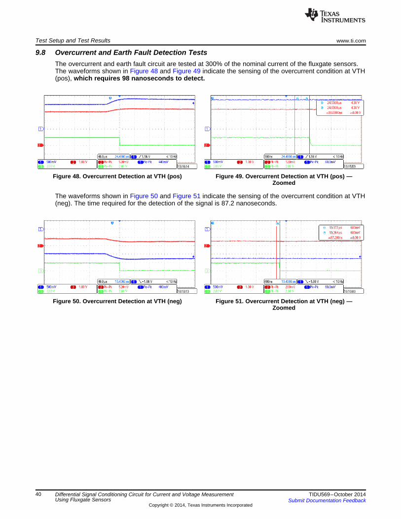
Test Setup and Test Results www.ti.com
9.8 Overcurrent and Earth Fault Detection TestsThe overcurrent and earth fault circuit are tested at 300% of the nominal current of the fluxgate sensors.The waveforms shown in Figure 48 and Figure 49 indicate the sensing of the overcurrent condition at VTH(pos), which requires 98 nanoseconds to detect.
Figure 48. Overcurrent Detection at VTH (pos) Figure 49. Overcurrent Detection at VTH (pos) —Zoomed
The waveforms shown in Figure 50 and Figure 51 indicate the sensing of the overcurrent condition at VTH(neg). The time required for the detection of the signal is 87.2 nanoseconds.
Figure 50. Overcurrent Detection at VTH (neg) Figure 51. Overcurrent Detection at VTH (neg) —Zoomed
40 Differential Signal Conditioning Circuit for Current and Voltage Measurement TIDU569–October 2014Using Fluxgate Sensors Submit Documentation Feedback
Copyright © 2014, Texas Instruments Incorporated

www.ti.com Test Setup and Test Results
The waveforms shown in Figure 52 and Figure 53 indicate the sensing of earth fault condition at VTH(pos). The time required for the detection of the signal is 92 nanoseconds.
Figure 52. Earth Fault Detection at VTH (pos) Figure 53. Earth Fault Detection at VTH (pos) — Zoomed
The waveforms shown in Figure 54 and Figure 55 indicate the sensing of the earth fault condition at VTH(neg). The time required for the detection of the signal is 98 nanoseconds.
Figure 54. Earth Fault Detection at VTH (neg) Figure 55. Earth Fault Detection at VTH (neg) — Zoomed
The comparators used in the protection circuits are open-drain outputs. The pull-up resistors areconnected to 3.3 V (which is typically equal to digital supply of the MCU or FPGA) so that the high and lowlevels of the comparator outputs are within the sensing range of the MCU or FPGA.
41TIDU569–October 2014 Differential Signal Conditioning Circuit for Current and Voltage MeasurementUsing Fluxgate SensorsSubmit Documentation Feedback
Copyright © 2014, Texas Instruments Incorporated

D1
MBRA160T3G
GND
AVDD
1
3
2
J5
PJ-102A
GND
DNC1
VIN2
TEMP3
GND4
TRIM/NR5
VOUT6
NC7
DNC8
U14
REF5025AID
1µFC21
AVDD
GND GND
1µF
C22
1.00kR34
GND
IN1
2
EN3
NC4
OUT5
GND
U10
TLV70033DCKR
1µFC8
GND
1µFC2
GND
GND
AVDD 3V3
+6V to +5V Conversion
+2.5V Reference
+5V to +3.3V Conversion
+6V Input +5V OutPut
GND
GND
AVDD
0
R35
0
R36 VREF_BUFVREF_BUF
1
2
J6
1751248
OUT1
NC2
SENSE3
6P4V24
6P4V15
3P2V6
GND7
1P6V8
0P8V9
0P4V10
0P2V11
0P1V12
EN13
NR14
IN15
IN16
NC17
NC18
NC19
OUT20
PAD21
U5
TPS7A4700RGW
10µFC4
10µFC9
10µFC3
10µFC13
GND
1µFC53
GNDGND
10µFC1
GND
AVDD
GND
1µFC14
GND
REF2025_REF/2
REF2025_REF
GND GND
0
R37DNP
0
R33
0R26
0R21
Green
A2
C1
LD1
GND
0R1
0R145
1
2
3
4
5
U15
OPA322AIDBVR
0.1µF
C25
GND
+2.5V Reference and +1.25V Bias supply
10µFC23
0.1µFC24DNP
0.1µFC20
0.1µFC15
VBIAS1
GND2
EN3
VIN4
VREF5
U13
REF2025DBV
REF2025_REF
REF2025_REF/2
1.00kR20
Design Files www.ti.com
10 Design Files
10.1 SchematicsTo download the schematics, see the design files at TIDA-00201.
Figure 56. Power Schematic
42 Differential Signal Conditioning Circuit for Current and Voltage Measurement TIDU569–October 2014Using Fluxgate Sensors Submit Documentation Feedback
Copyright © 2014, Texas Instruments Incorporated

GND
GND
AVDD
GND
OUT1
OUT1
GND
REF_AINA1
0R69
AIN1M
0R68
AINM_A
CH1 SIGNAL CONDITIONING
7
1
8
5
VOCM2
4
V+
V-
36 U20
THS4531IDGK
0R108
0
R106
10
R90
10
R89REF_AINA1
1
2345
J14
142-0701-201
GND
0R75
AIN1P
0R74
AINP_A
AVDD
1µFC57
GND
0R149
DNP
VREF_BUFVREF_BUF
0.039µFC44DNP
0.01µFC29
0.1µF
C36
1
2
J4
1751248
1
2345
J13
142-0701-201
IN2
2
IN3
3
IN4
4
IN5
5O
UT
16
OU
T2
7
OU
T3
8
OU
T4
9
Vref11
Vout12
GND13
UC14
IN1
1O
UT
510
U4
AINP_A
AIN1P
AINM_A
AIN1M
OUT1
CH2 SIGNAL CONDITIONING
GND
GND
AVDD
0.1µF
C35
1
2345
J11
142-0701-201
GND
OUT2
OUT2
GND
REF_AINA2
GND
IN2
2
IN3
3
IN4
4
IN5
5O
UT
16
OU
T2
7
OU
T3
8
OU
T4
9
Vref11
Vout12
GND13
UC14
IN1
1O
UT
510
U3
1
2
J3
1751248
0R66
AIN2M
0R67
AINM_B
7
1
8
5
VOCM2
4
V+
V-
36 U19
THS4531IDGK
0R104
0
R102
10
R88
10
R87REF_AINA2
1
2345
J12
142-0701-201
GND
0R73
AIN2P
0R72
AINP_B
AVDD
1µFC56
GND
0R148
DNP
VREF_BUFVREF_BUF
0.039µF
C43DNP
0.01µFC28
AINP_B
AIN2P
AINM_B
AIN2M
OUT2
1µFC39
CH1 OVERCURRENT FAULT DETECTION
CH2 OVERCURRENT FAULT DETECTION
GND
1µFC40
0.039µFC52
GND
0
R135
0R123DNP
REF2025_REF/2
0
R134
0R122
DNP
REF2025_REF/2
0.039µFC51
GND
REF2025_REF/2
0.039µFC47
GND
0.039µFC48
GND
3
2
1
84
U9ATLC372
5
6
7
U9BTLC372
GND
AVDD
GND
0.1µF
C10
GNDOUT1
AVDD
OC_FAULTOC_FAULT
3.30kR11
3.30kR13
20.0kR12
3
2
1
84
U8ATLC372
5
6
7
U8BTLC372
GND
AVDD
GND
0.1µF
C6
GNDOUT2
AVDD
OC_FAULT
3.30kR8
3.30kR10
20.0kR9
0
R120
0
R119
0R118
0R117
205
R144
205
R143
205
R142
205
R141
7.87k
R128
7.87k
R132
7.87k
R127
7.87k
R131
10.9k
R109
10.9k
R107
10.9k
R105
10.9k
R103
1000pFC60
1000pFC61
1000pFC62
1000pFC63
www.ti.com Design Files
Figure 57. Channel 1 and 2 Schematic
43TIDU569–October 2014 Differential Signal Conditioning Circuit for Current and Voltage MeasurementUsing Fluxgate SensorsSubmit Documentation Feedback
Copyright © 2014, Texas Instruments Incorporated

CH3 SIGNAL CONDITIONING
GND
GND
AVDD
0.1µF
C34
1
2345
J9
142-0701-201
GND
OUT3
OUT3
GND
REF_AINA3
GND
IN2
2
IN3
3
IN4
4
IN5
5O
UT
16
OU
T2
7
OU
T3
8
OU
T4
9
Vref11
Vout12
GND13
UC14
IN1
1O
UT
51
0
U2
1
2
J2
1751248
0R65
AIN3M
7
1
8
5
VOCM2
4
V+
V-
36 U18
THS4531IDGK
0R100
0R98
10
R86
10
R85REF_AINA3
1
2345
J10
142-0701-201
GND
0R71
AIN3P
AVDD
1µFC55
GND
0R147
DNP
VREF_BUFVREF_BUF
0R70
AINP_C
0R64
AINM_C
0.039µFC42DNP
0.01µFC27
AINP_C
AIN3P
AIN3M
AINM_C
OUT3
1µFC38
CH4 SIGNAL CONDITIONING
GND
GND
AVDD
0.1µF
C33
1
2345
J7
142-0701-201
GND
OUT4
OUT4
GND
REF_AINA4
GND
IN2
2
IN3
3
IN4
4
IN5
5O
UT
16
OU
T2
7
OU
T3
8
OU
T4
9
Vref11
Vout12
GND13
UC14
IN1
1O
UT
510
U1
1
2
J1
1751248
0R76
AIN4M
7
1
8
5
VOCM2
4
V+
V-
36 U17
THS4531IDGK
0R96
0R94
10
R84
10
R83REF_AINA4
1
2345
J8
142-0701-201
GND
0R78
AIN4P
AVDD
1µFC54
GND
0R146
DNP
VREF_BUFVREF_BUF
0R79
AINP_D
0R77
AINM_D
0.039µF
C41DNP
0.01µFC26
AINP_D
AIN4P
AIN4M
AINM_D
OUT4
1µFC37
CH3 OVERCURRENT FAULT DETECTION
CH4 OVERCURRENT FAULT DETECTION
OC_FAULTOC_FAULT
3V3
Green
A2
C1
LD3
10kR45
0
R133
0R121DNP
REF2025_REF/2
0.039µFC50
GND
0R136
0R124
DNP
REF2025_REF/2
0.039µF
C49
GND
REF2025_REF/2
0.039µFC46
GND
0.039µF
C45
GND
3
2
1
84
U7ATLC372
5
6
7
U7BTLC372
GND
AVDD
GND
0.1µF
C7
GNDOUT3
AVDD
3.30kR5
3.30kR7
20.0kR6
3
2
1
84
U6ATLC372
5
6
7
U6BTLC372
GND
AVDD
GND
0.1µF
C5
GNDOUT4
AVDD
OC_FAULT
3.30kR2
3.30kR4
20.0kR3
0R116
0R115
0R114
0R113
205
R140
205
R139
205
R138
205
R137
7.87k
R126
7.87k
R130
7.87k
R125
7.87k
R129
10.9k
R101
10.9k
R99
10.9k
R97
10.9k
R95
1000pFC64
1000pFC65
1000pFC66
1000pFC67
Design Files www.ti.com
Figure 58. Channel 3 and 4 Schematic
44 Differential Signal Conditioning Circuit for Current and Voltage Measurement TIDU569–October 2014Using Fluxgate Sensors Submit Documentation Feedback
Copyright © 2014, Texas Instruments Incorporated

AINP_A
10µFC19
10µFC16
GND
AINP_B
0R15
10µFC12
GND
47R17
47R23
47R82
47R81
47R31
0R28
10µFC30
GND
100kR32
DNP
GND
AVDD
3V3
TWO ADS7854s FOR INTERFACING WITH EX TERNAL MOTOR CONTROLLER
AINP_A1
AINM_A2
REFIO_A3
REFGND_A4
REFGND_B5
REFIO_B6
AINM_B7
AINP_B8
DVDD9
SDI10
CS11
SCLK12
AVDD16
GND15
SDO_B14
SDO_A13
U12
ADS7854
0.22R24
0.22R19
AINM_A
AINM_B SDI
CS
SCLK
SDO_A_1
SDO_B_1
AINP_A
AINM_A
AINM_B
AINP_B
GROUND FAULT DETECTION
AINP_C
10µFC17
10µFC18
GND
AINP_D
0R14
10µFC11
GND
47R16
47R22
0R27
10µFC31
GND
AVDD
3V3
AINP_A1
AINM_A2
REFIO_A3
REFGND_A4
REFGND_B5
REFIO_B6
AINM_B7
AINP_B8
DVDD9
SDI10
CS11
SCLK12
AVDD16
GND15
SDO_B14
SDO_A13
U11
ADS7854
0.22R18
0.22R25
AINM_C
AINM_D SDI 1
CS 1
SCLK1
SDO_A_2
SDO_B_2
AINP_C
AINM_C
AINM_D
AINP_D
GND_FAULTOC_FAULT 1
2
J17
282834-2
1
2
3
4
5
6
7
8
J19
HEADER_1X8
SCLK
CS
GND
SDO_B_1
SDO_A_1
SDO_B_2
SDO_A_2
VREF_BUFVREF_BUF
VREF_BUFVREF_BUF
VREF_BUFVREF_BUF
VREF_BUFVREF_BUF
SCLK1
CS 1
SDI 1
0R30
0R29
0R80
GND_FAULT
OC_FAULT
3V3
Green
A2
C1
LD2
10kR44
1.0k
R112
1.0k
R111
OUT1
OUT2
OUT3
OUT1
OUT2
OUT31.0k
R110
GND_FAULT
SCLK
SDISDI
SDO_A_1
SDO_A_2
SDO_B_1
SDO_B_2
CS
1
2
3
4
5
6
7
8
9
10
11
12
J18
HEADER_1X12
REF2025_REF
REF2025_REF/2
REF2025_REF
REF2025_REF/2
AINP_A
AINM_A
AINM_B
AINP_B
AINM_C
AINP_C
AINM_D
AINP_DGND
3V3
0
R46
3
2
1
84
U16ATLC372
5
6
7
U16BTLC372
GND
AVDD
GND
0.1µF
C32
GND
AVDD
3.30kR91
3.30kR93
20.0kR92
0R150DNP
0R151DNP
0R152DNP
0R153DNP
www.ti.com Design Files
Figure 59. ADC Connectors Schematic
45TIDU569–October 2014 Differential Signal Conditioning Circuit for Current and Voltage MeasurementUsing Fluxgate SensorsSubmit Documentation Feedback
Copyright © 2014, Texas Instruments Incorporated

1 2
3 4
5 6
7 8
9 10
11 12
13 14
15 16
17 18
19 20
21 22
23 24
25 26
27 28
29 30
31 32
33 34
35 36
37 38
39 40
41 42
43 44
45 46
47 48
49 50
51 52
53 54
55 56
57 58
59 60
J16A
SPD08-120-L-RB
61 62
63 64
65 66
67 68
69 70
71 72
73 74
75 76
77 78
79 80
81 82
83 84
85 86
87 88
89 90
91 92
93 94
95 96
97 98
99 100
101 102
103 104
105 106
107 108
109 110
111 112
113 114
115 116
117 118
119 120
J16B
SPD08-120-L-RB121
123
125
127
129
131
133
135
137
139
141
143
145
147
149
151
153
155
157
159
161
163
165
167
169
171
173
175
177
179
122
124
126
128
130
132
134
136
138
140
142
144
146
148
150
152
154
156
158
160
162
164
166
168
170
172
174
176
178
180
J15SPD08-060-RB-TR
0R560R55
DNPSDO_B_2SDO_A_2
0R63SDI
0R40SCLK
0R41SCLK
0R59CS
0R54
0R47
AVDD
AVDD
GND
0R42
SCLK
SDI
SDO_A_2
SDO_B_2
CS
0R58REF2025_REF/2
0R57REF2025_REFREF2025_REF
REF2025_REF/2
AIN2MAIN2M
AIN2PAIN2P
0R52
0R53
AIN3P
AIN3MAIN3M
AIN3P0R48
0R49
AIN4P
AIN4MAIN4M
AIN4P0R60
0R61
0R43
GND
3.6VD3
3.6VD4
3.6VD8
3.6VD7
3.6VD5
3.6VD9
GND
GND
1µFC58
1µFC59
GND
GND
AIN1M
AIN1P
0R51
0R50AIN1P
AIN1M
3.6VD2
3.6VD6
GND
0R154
0R155
0R156
0R157
0R158
0R159
0R160
0R161
GND
GND
GND
GND
GND
GND
GND
GND
0R62SDI
SDO_B_1SDO_A_1
0R38DNP
0R39SDO_A_1
SDO_B_1
Design Files www.ti.com
Figure 60. 180-Pin Connector Interface Schematic
46 Differential Signal Conditioning Circuit for Current and Voltage Measurement TIDU569–October 2014Using Fluxgate Sensors Submit Documentation Feedback
Copyright © 2014, Texas Instruments Incorporated
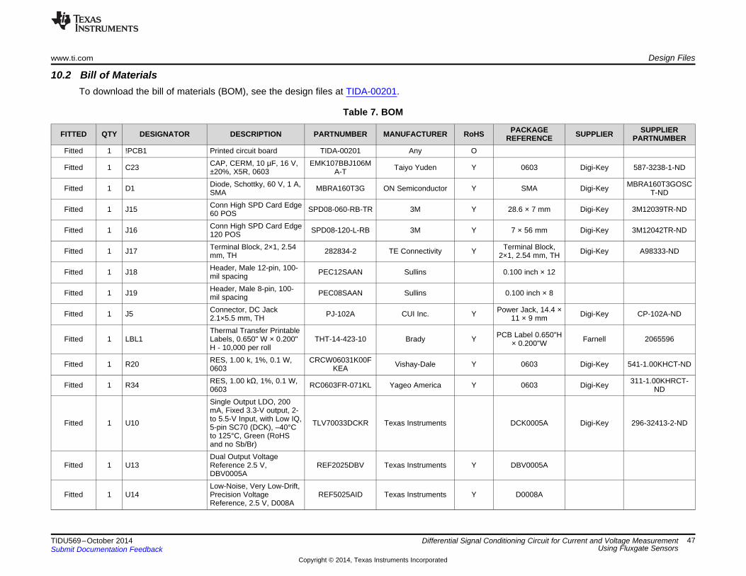
www.ti.com Design Files
10.2 Bill of MaterialsTo download the bill of materials (BOM), see the design files at TIDA-00201.
Table 7. BOM
PACKAGE SUPPLIERFITTED QTY DESIGNATOR DESCRIPTION PARTNUMBER MANUFACTURER RoHS SUPPLIERREFERENCE PARTNUMBERFitted 1 !PCB1 Printed circuit board TIDA-00201 Any O
CAP, CERM, 10 µF, 16 V, EMK107BBJ106MFitted 1 C23 Taiyo Yuden Y 0603 Digi-Key 587-3238-1-ND±20%, X5R, 0603 A-TDiode, Schottky, 60 V, 1 A, MBRA160T3GOSCFitted 1 D1 MBRA160T3G ON Semiconductor Y SMA Digi-KeySMA T-NDConn High SPD Card EdgeFitted 1 J15 SPD08-060-RB-TR 3M Y 28.6 × 7 mm Digi-Key 3M12039TR-ND60 POSConn High SPD Card EdgeFitted 1 J16 SPD08-120-L-RB 3M Y 7 × 56 mm Digi-Key 3M12042TR-ND120 POSTerminal Block, 2×1, 2.54 Terminal Block,Fitted 1 J17 282834-2 TE Connectivity Y Digi-Key A98333-NDmm, TH 2×1, 2.54 mm, THHeader, Male 12-pin, 100-Fitted 1 J18 PEC12SAAN Sullins 0.100 inch × 12mil spacingHeader, Male 8-pin, 100-Fitted 1 J19 PEC08SAAN Sullins 0.100 inch × 8mil spacingConnector, DC Jack Power Jack, 14.4 ×Fitted 1 J5 PJ-102A CUI Inc. Y Digi-Key CP-102A-ND2.1×5.5 mm, TH 11 × 9 mmThermal Transfer Printable PCB Label 0.650"HFitted 1 LBL1 Labels, 0.650" W × 0.200" THT-14-423-10 Brady Y Farnell 2065596× 0.200"WH - 10,000 per rollRES, 1.00 k, 1%, 0.1 W, CRCW06031K00FFitted 1 R20 Vishay-Dale Y 0603 Digi-Key 541-1.00KHCT-ND0603 KEARES, 1.00 kΩ, 1%, 0.1 W, 311-1.00KHRCT-Fitted 1 R34 RC0603FR-071KL Yageo America Y 0603 Digi-Key0603 NDSingle Output LDO, 200mA, Fixed 3.3-V output, 2-to 5.5-V Input, with Low IQ,Fitted 1 U10 TLV70033DCKR Texas Instruments DCK0005A Digi-Key 296-32413-2-ND5-pin SC70 (DCK), –40°Cto 125°C, Green (RoHSand no Sb/Br)Dual Output Voltage
Fitted 1 U13 Reference 2.5 V, REF2025DBV Texas Instruments Y DBV0005ADBV0005ALow-Noise, Very Low-Drift,
Fitted 1 U14 Precision Voltage REF5025AID Texas Instruments Y D0008AReference, 2.5 V, D008A
47TIDU569–October 2014 Differential Signal Conditioning Circuit for Current and Voltage MeasurementUsing Fluxgate SensorsSubmit Documentation Feedback
Copyright © 2014, Texas Instruments Incorporated

Design Files www.ti.com
Table 7. BOM (continued)PACKAGE SUPPLIERFITTED QTY DESIGNATOR DESCRIPTION PARTNUMBER MANUFACTURER RoHS SUPPLIERREFERENCE PARTNUMBER
20 MHz, Low Noise, RRIO,CMOS OperationalAmplifier with Shutdown,
Fitted 1 U15 1.8 to 5.5 V, –40°C to OPA322AIDBVR Texas Instruments DBV0005A Digi-Key 296-29488-2-ND125°C, 5-pin SOT23(DBV0005A), Green(RoHS & no Sb/Br)36-V, 1-A, 4.17-µVRMS, RFFitted 1 U5 TPS7A4700RGW Texas Instruments Y RGW0020ALDO, RGW0020A
C37, C38, C39, C40, CAP, CERM, 1 µF, 25 V, GRM188R71E105Fitted 10 C54, C55, C56, C57, MuRata Y 0603 Digi-Key 490-5307-1-ND±10%, X7R, 0603 KA12DC58, C59C5, C6, C7, C10, C25, CAP, CERM, 0.1 µF, 16 V, C0603C104J4RACFitted 10 C32, C33, C34, C35, Kemet Y 0603 Digi-Key 399-1097-1-ND±5%, X7R, 0603 TUC36R2, R4, R5, R7, R8, RES, 3.30 kΩ, 1%, 0.1 W, RC0603FR- 311-3.30KHRCT-Fitted 10 R10, R11, R13, R91, Yageo America Y 0603 Digi-Key0603 073K3L NDR93
CAP, CERM, 0.1 µF, 10 V, C0603C104K8RACFitted 2 C15, C20 Kemet Y 0603 Digi-Key 399-1095-1-ND±10%, X7R, 0603 TURES, 10 kΩ, 5%, 0.1 W, CRCW060310K0JFitted 2 R44, R45 Vishay-Dale Y 0603 Digi-Key 541-10KGCT-ND0603 NEAIC ADC 12-BIT 1MSPSFitted 2 U11, U12 ADS7854 Texas Instruments Y 16TSSOPDual 16TSSOPLED SmartLED Green 570 LG L29K-G2J1-24-Fitted 3 LD1, LD2, LD3 OSRAM 0603 Digi-Key 475-2709-2-NDNM ZRES, 1.0 kΩ, 5%, 0.1 W, CRCW06031K00J 71-CRCW0603J-Fitted 3 R110, R111, R112 Vishay-Dale Y 0603 Mouser0603 NEA 1.0K-E3CAP, CERM, 0.01 µF, 16 GRM188R71C103Fitted 4 C26, C27, C28, C29 MuRata Y 0603 Digi-Key 490-1525-1-NDV, ±10%, X7R, 0603 KA01DMachine Screw, Round, NY PMS 440 0025 BandF FastenerFitted 4 H1, H2, H3, H4 #4–40 × 1/4, Nylon, Philips Y Screw Digi-Key H542-NDPH SupplypanheadStandoff, Hex, 0.5"L #4–40Fitted 4 H5, H6, H7, H8 1902C Keystone Y Standoff Digi-Key 1902CK-NDNylonRES, 0.22 Ω, 1%, 0.1 W,Fitted 4 R18, R19, R24, R25 ERJ-3RQFR22V Panasonic Y 0603 Digi-Key P.22AJDKR-ND0603Sensor Current 50-A, 5-VFitted 4 U1, U2, U3, U4 CKSR X-NP LEM USA Inc Y Module Digi-Key 98-1098-5-NDMOD
48 Differential Signal Conditioning Circuit for Current and Voltage Measurement TIDU569–October 2014Using Fluxgate Sensors Submit Documentation Feedback
Copyright © 2014, Texas Instruments Incorporated

www.ti.com Design Files
Table 7. BOM (continued)PACKAGE SUPPLIERFITTED QTY DESIGNATOR DESCRIPTION PARTNUMBER MANUFACTURER RoHS SUPPLIERREFERENCE PARTNUMBER
Ultra Low Power, Rail-to-Rail Output, Fully-Fitted 4 U17, U18, U19, U20 THS4531IDGK Texas Instruments Y DGK0008ADifferential Amplifier,DGK0008ACAP, CERM, 10 µF, 16 V, GRM21BR61C106Fitted 5 C1, C3, C4, C9, C13 MuRata Y 0805 Digi-Key 490-3886-1-ND±10%, X5R, 0805 KE15LConn Term Block, 2POS,Fitted 5 J1, J2, J3, J4, J6 1751248 Phoenix Contact Y 11 × 8.5 × 7.3 mm Digi-Key 277-5719-ND3.5 mm, THRES, 20.0 kΩ, 1%, 0.1 W, CRCW060320K0FFitted 5 R3, R6, R9, R12, R92 Vishay-Dale Y 0603 Digi-Key 541-20.0KHCT-ND0603 KEAIC, Dual DifferentialFitted 5 U6, U7, U8, U9, U16 TLC372 Texas Instruments SO-8Comparators, 2 to 36 Vin
C2, C8, C14, C21, CAP, CERM, 1 µF, 10 V, C0805C105K8RACFitted 6 Kemet Y 0805 Digi-Key 399-1172-1-NDC22, C53 ±10%, X7R, 0805 TUFID1, FID2, FID3, Fiducial mark. There isFitted 6 N/A N/A FiducialFID4, FID5, FID6 nothing to buy or mount.R16, R17, R22, R23, RES, 47 Ω, 5%, 0.1 W, CRCW060347R0JFitted 7 Vishay-Dale Y 0603 Digi-Key 541-47GCT-NDR31, R81, R82 0603 NEAC11, C12, C16, C17, CAP, CERM, 10 µF, 25 V, C1608X5R1E106MFitted 8 TDK Y 0603 Digi-Key 445-9015-1-NDC18, C19, C30, C31 ±20%, X5R, 0603 080ACC45, C46, C47, C48, CAP, CERM, 0.039 µF, 16 GRM188R71C393 GRM188R71C393Fitted 8 MuRata Y 0603 Digi-KeyC49, C50, C51, C52 V, ±10%, X7R, 0603 KA01D KA01D-NDC60, C61, C62, C63, CAP, CERM, 1000 pF, 16 GRM188R71C102 GRM188R71C102Fitted 8 MuRata Y 0603 Digi-KeyC64, C65, C66, C67 V, ±10%, X7R, 0603 KA01D KA01D-NDD2, D3, D4, D5, D6, Diode, Zener, 3.6 V, 500 MMSZ5227B-Fitted 8 MMSZ5227B-7-F Diodes Inc. Y SOD-123 Digi-KeyD7, D8, D9 mW, SOD-123 FDICT-NDJ7, J8, J9, J10, J11, Emerson NetworkFitted 8 Connector, TH, SMA 142-0701-201 Y SMA Digi-Key J500-NDJ12, J13, J14 PowerR125, R126, R127, RES, 7.87 k, 1%, 0.1 W, CRCW06037K87FFitted 8 R128, R129, R130, Vishay-Dale Y 0603 Digi-Key 541-7.87KHCT-ND0603 KEAR131, R132R137, R138, R139, RES, 205, 1%, 0.1 W, CRCW0603205RFFitted 8 R140, R141, R142, Vishay-Dale Y 0603 Digi-Key 541-205HCT-ND0603 KEAR143, R144R83, R84, R85, R86, RES, 10 Ω, 5%, 0.1W, CRCW060310R0JFitted 8 Vishay-Dale Y 0603 Digi-Key 541-10GCT-NDR87, R88, R89, R90 0603 NEAR95, R97, R99, R101, RES, 10.9 k, 0.5%, 0.1 W, RT0603DRE0710KFitted 8 R103, R105, R107, Yageo America Y 06030603 9LR109
49TIDU569–October 2014 Differential Signal Conditioning Circuit for Current and Voltage MeasurementUsing Fluxgate SensorsSubmit Documentation Feedback
Copyright © 2014, Texas Instruments Incorporated

Design Files www.ti.com
Table 7. BOM (continued)PACKAGE SUPPLIERFITTED QTY DESIGNATOR DESCRIPTION PARTNUMBER MANUFACTURER RoHS SUPPLIERREFERENCE PARTNUMBER
R1, R14, R15, R21,R26, R27, R28, R29,R30, R33, R35, R36,R39, R40, R41, R42,R43, R46, R47, R48,R49, R50, R51, R52,R53, R54, R56, R57,R58, R59, R60, R61,R62, R63, R64, R65,R66, R67, R68, R69,R70, R71, R72, R73, RES, 0 Ω, 5%, 0.1 W, CRCW06030000Z0Fitted 80 Vishay-Dale Y 0603 Digi-Key 541-0.0GCT-NDR74, R75, R76, R77, 0603 EAR78, R79, R80, R94,R96, R98, R100, R102,R104, R106, R108,R113, R114, R115,R116, R117, R118,R119, R120, R133,R134, R135, R136,R145, R154, R155,R156, R157, R158,R159, R160, R161
CAP, CERM, 0.1 µF, 10 V, C0603C104K8RACNot Fitted 0 C24 Kemet Y 0603 Digi-Key 399-1095-1-ND±10%, X7R, 0603 TUCAP, CERM, 0.039 µF, 16 GRM188R71C393 GRM188R71C393Not Fitted 0 C41, C42, C43, C44 MuRata Y 0603 Digi-KeyV, ±10%, X7R, 0603 KA01D KA01D-NDRES, 100 kΩ, 1%, 0.1 W, CRCW0603100KFNot Fitted 0 R32 Vishay-Dale Y 0603 Digi-Key 541-100KHCT-ND0603 KEA
R37, R38, R55, R121,R122, R123, R124, RES, 0 Ω, 5%, 0.1 W, CRCW06030000Z0Not Fitted 0 R146, R147, R148, Vishay-Dale Y 0603 Digi-Key 541-0.0GCT-ND0603 EAR149, R150, R151,R152, R153
50 Differential Signal Conditioning Circuit for Current and Voltage Measurement TIDU569–October 2014Using Fluxgate Sensors Submit Documentation Feedback
Copyright © 2014, Texas Instruments Incorporated

www.ti.com Design Files
10.3 PCB Layout
NOTE: The total dimension of the board is 112 × 90 mm.
10.3.1 Layout Guidelines
Layout of Amplifier SectionThe THS4531 datasheet provides some general guidelines for the layout of the external components nearthe amplifier, ground plane construction, and power routing:1. Keep signal routing direct and as short as possible into and out of the op-amp.2. Make the feedback path short and direct to avoid vias if possible.3. Remove the ground or power planes from directly under the amplifier’s input and output pins.4. Place a series output resistor as near to the output pin as possible.5. Place a power supply decoupling capacitor within 2 inches of the device and share with other op-amps.
For a split supply, use a capacitor for both supplies.6. Place a 0.1-μF power supply decoupling capacitor as near to the power supply pins as possible,
preferably within 0.1 inch. For a split supply, use a capacitor for both supplies.7. The PD pin uses TTL logic levels referenced to the negative supply voltage (VS–). When not used, tie
the PD pin to the positive supply to enable the amplifier. When used, actively drive the pin high or low,and do not leave it in an indeterminate logic state. Although it is not required, use a bypass capacitorfor robustness in noisy environments.
Layout of ADC SectionThe most important considerations in designing the PCB layout are as follows:1. Keep the length of traces from the reference buffer circuit (REF, THS, and OPA) to the REFP input pin
of the ADC as small as possible to minimize the trace inductance that can lead to instability andpotential issues with the accurate settling of the reference voltage.
2. Locate the input driver circuit, comprised of the THS4521, as close as possible to the inputs of theADC to minimize loop area, making the layout more robust against EMI/RFI rejection. Similarly, keepthe resistors and capacitor of the anti-aliasing filter at the inputs of the ADC close together and close tothe inputs of the ADC to minimize the loop area.
3. Keep the traces feeding the differential input voltage from the source up to the differential inputs of theADC symmetrical without any sharp turns.
51TIDU569–October 2014 Differential Signal Conditioning Circuit for Current and Voltage MeasurementUsing Fluxgate SensorsSubmit Documentation Feedback
Copyright © 2014, Texas Instruments Incorporated

Design Files www.ti.com
10.3.2 Layer PlotsTo download the layer plots, see the design files at TIDA-00201.
Figure 61. Top Overlay Figure 62. Top Solder
Figure 63. Top Layer Figure 64. Top Paste
52 Differential Signal Conditioning Circuit for Current and Voltage Measurement TIDU569–October 2014Using Fluxgate Sensors Submit Documentation Feedback
Copyright © 2014, Texas Instruments Incorporated

www.ti.com Design Files
Figure 65. Bottom Paste Figure 66. Bottom Layer
Figure 67. Bottom Solder Figure 68. Bottom Overlay
53TIDU569–October 2014 Differential Signal Conditioning Circuit for Current and Voltage MeasurementUsing Fluxgate SensorsSubmit Documentation Feedback
Copyright © 2014, Texas Instruments Incorporated

Design Files www.ti.com
Figure 69. M1 Board Outline
54 Differential Signal Conditioning Circuit for Current and Voltage Measurement TIDU569–October 2014Using Fluxgate Sensors Submit Documentation Feedback
Copyright © 2014, Texas Instruments Incorporated

www.ti.com Design Files
10.4 Altium ProjectTo download the Altium project files, see the design files at TIDA-00201.
Figure 70. Top Layer Figure 71. PWR Layer
Figure 72. GND Layer Figure 73. Bottom Layer
55TIDU569–October 2014 Differential Signal Conditioning Circuit for Current and Voltage MeasurementUsing Fluxgate SensorsSubmit Documentation Feedback
Copyright © 2014, Texas Instruments Incorporated

Design Files www.ti.com
10.5 Gerber FilesTo download the Gerber files, see the design files at TIDA-00201.
Figure 74. Fabrication Drawing
56 Differential Signal Conditioning Circuit for Current and Voltage Measurement TIDU569–October 2014Using Fluxgate Sensors Submit Documentation Feedback
Copyright © 2014, Texas Instruments Incorporated
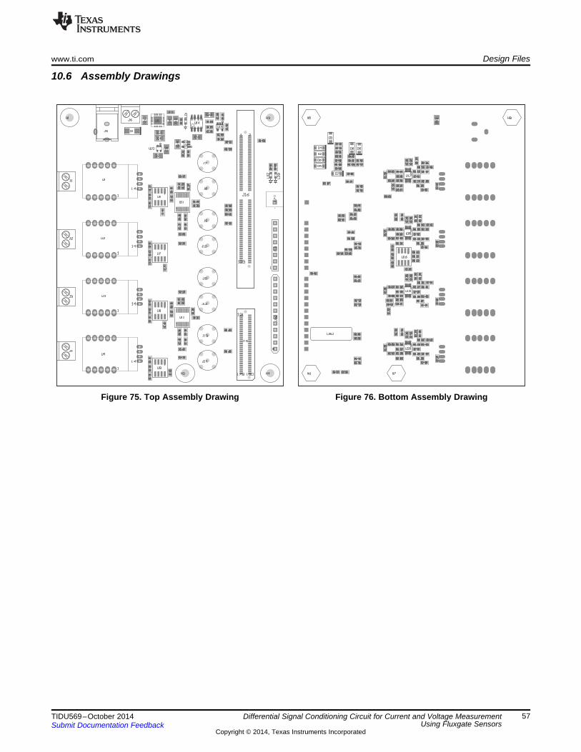
www.ti.com Design Files
10.6 Assembly Drawings
Figure 75. Top Assembly Drawing Figure 76. Bottom Assembly Drawing
57TIDU569–October 2014 Differential Signal Conditioning Circuit for Current and Voltage MeasurementUsing Fluxgate SensorsSubmit Documentation Feedback
Copyright © 2014, Texas Instruments Incorporated
References www.ti.com
11 References
1. LEM Technologies (Link).2. Dominggus Yosua Suitella, Dr. Ir. Djoko Windarto, MT, High Precision Fluxgate Current Sensor (PDF).3. Krzysztof Iniewski, ed. Smart Sensors for Industrial Applications, CRC Press.4. Vaibhav Kumar. 18-Bit, 1MSPS Data Acquisition Block (DAQ) Optimized for Lowest Distortion and
Noise, Texas Instruments (SLAU515).5. Data Acquisition at 1KHz AC, 1mW, 18bit, 1Msps Reference Design, Texas Instruments (Tool Folder).6. FilterPro™ Software (Link)7. Current Transducer CKSR series Datasheet, LEM Technologies (PDF)8. Industry Current & Voltage Transducers Industry Catalog, LEM Technologies (PDF)9. ADSxx54 Dual, High-Speed, 16-, 14-, and 12-Bit, Simultaneous-Sampling, Analog-to-Digital
Converters, Texas Instruments (SBAS556)
12 About the AuthorSANJAY PITHADIA is a systems engineer at Texas Instruments where he is responsible for developingsubsystem design solutions for the Industrial Motor Drive segment. Sanjay has been with TI since 2008and has been involved in designing products related to energy and smart grid. Sanjay brings to this rolehis experience in analog design, mixed signal design, industrial interfaces, and power supplies. Sanjayearned his bachelor of technology in electronics engineering at VJTI, Mumbai.
N. NAVANEETH KUMAR is a systems architect at Texas Instruments where he is responsible fordeveloping subsystem solutions for motor controls within Industrial Systems. N. Navaneeth brings to thisrole his extensive experience in power electronics, EMC, analog, and mixed signal designs. He hassystem-level product design experience in drives, solar inverters, UPS, and protection relays. N.Navaneeth earned his bachelor of electronics and communication engineering from Bharathiar University,India and his master of science in electronic product development from Bolton University, UK.
58 Differential Signal Conditioning Circuit for Current and Voltage Measurement TIDU569–October 2014Using Fluxgate Sensors Submit Documentation Feedback
Copyright © 2014, Texas Instruments Incorporated
IMPORTANT NOTICE FOR TI REFERENCE DESIGNS
Texas Instruments Incorporated ("TI") reference designs are solely intended to assist designers (“Buyers”) who are developing systems thatincorporate TI semiconductor products (also referred to herein as “components”). Buyer understands and agrees that Buyer remainsresponsible for using its independent analysis, evaluation and judgment in designing Buyer’s systems and products.TI reference designs have been created using standard laboratory conditions and engineering practices. TI has not conducted anytesting other than that specifically described in the published documentation for a particular reference design. TI may makecorrections, enhancements, improvements and other changes to its reference designs.Buyers are authorized to use TI reference designs with the TI component(s) identified in each particular reference design and to modify thereference design in the development of their end products. HOWEVER, NO OTHER LICENSE, EXPRESS OR IMPLIED, BY ESTOPPELOR OTHERWISE TO ANY OTHER TI INTELLECTUAL PROPERTY RIGHT, AND NO LICENSE TO ANY THIRD PARTY TECHNOLOGYOR INTELLECTUAL PROPERTY RIGHT, IS GRANTED HEREIN, including but not limited to any patent right, copyright, mask work right,or other intellectual property right relating to any combination, machine, or process in which TI components or services are used.Information published by TI regarding third-party products or services does not constitute a license to use such products or services, or awarranty or endorsement thereof. Use of such information may require a license from a third party under the patents or other intellectualproperty of the third party, or a license from TI under the patents or other intellectual property of TI.TI REFERENCE DESIGNS ARE PROVIDED "AS IS". TI MAKES NO WARRANTIES OR REPRESENTATIONS WITH REGARD TO THEREFERENCE DESIGNS OR USE OF THE REFERENCE DESIGNS, EXPRESS, IMPLIED OR STATUTORY, INCLUDING ACCURACY ORCOMPLETENESS. TI DISCLAIMS ANY WARRANTY OF TITLE AND ANY IMPLIED WARRANTIES OF MERCHANTABILITY, FITNESSFOR A PARTICULAR PURPOSE, QUIET ENJOYMENT, QUIET POSSESSION, AND NON-INFRINGEMENT OF ANY THIRD PARTYINTELLECTUAL PROPERTY RIGHTS WITH REGARD TO TI REFERENCE DESIGNS OR USE THEREOF. TI SHALL NOT BE LIABLEFOR AND SHALL NOT DEFEND OR INDEMNIFY BUYERS AGAINST ANY THIRD PARTY INFRINGEMENT CLAIM THAT RELATES TOOR IS BASED ON A COMBINATION OF COMPONENTS PROVIDED IN A TI REFERENCE DESIGN. IN NO EVENT SHALL TI BELIABLE FOR ANY ACTUAL, SPECIAL, INCIDENTAL, CONSEQUENTIAL OR INDIRECT DAMAGES, HOWEVER CAUSED, ON ANYTHEORY OF LIABILITY AND WHETHER OR NOT TI HAS BEEN ADVISED OF THE POSSIBILITY OF SUCH DAMAGES, ARISING INANY WAY OUT OF TI REFERENCE DESIGNS OR BUYER’S USE OF TI REFERENCE DESIGNS.TI reserves the right to make corrections, enhancements, improvements and other changes to its semiconductor products and services perJESD46, latest issue, and to discontinue any product or service per JESD48, latest issue. Buyers should obtain the latest relevantinformation before placing orders and should verify that such information is current and complete. All semiconductor products are soldsubject to TI’s terms and conditions of sale supplied at the time of order acknowledgment.TI warrants performance of its components to the specifications applicable at the time of sale, in accordance with the warranty in TI’s termsand conditions of sale of semiconductor products. Testing and other quality control techniques for TI components are used to the extent TIdeems necessary to support this warranty. Except where mandated by applicable law, testing of all parameters of each component is notnecessarily performed.TI assumes no liability for applications assistance or the design of Buyers’ products. Buyers are responsible for their products andapplications using TI components. To minimize the risks associated with Buyers’ products and applications, Buyers should provideadequate design and operating safeguards.Reproduction of significant portions of TI information in TI data books, data sheets or reference designs is permissible only if reproduction iswithout alteration and is accompanied by all associated warranties, conditions, limitations, and notices. TI is not responsible or liable forsuch altered documentation. Information of third parties may be subject to additional restrictions.Buyer acknowledges and agrees that it is solely responsible for compliance with all legal, regulatory and safety-related requirementsconcerning its products, and any use of TI components in its applications, notwithstanding any applications-related information or supportthat may be provided by TI. Buyer represents and agrees that it has all the necessary expertise to create and implement safeguards thatanticipate dangerous failures, monitor failures and their consequences, lessen the likelihood of dangerous failures and take appropriateremedial actions. Buyer will fully indemnify TI and its representatives against any damages arising out of the use of any TI components inBuyer’s safety-critical applications.In some cases, TI components may be promoted specifically to facilitate safety-related applications. With such components, TI’s goal is tohelp enable customers to design and create their own end-product solutions that meet applicable functional safety standards andrequirements. Nonetheless, such components are subject to these terms.No TI components are authorized for use in FDA Class III (or similar life-critical medical equipment) unless authorized officers of the partieshave executed an agreement specifically governing such use.Only those TI components that TI has specifically designated as military grade or “enhanced plastic” are designed and intended for use inmilitary/aerospace applications or environments. Buyer acknowledges and agrees that any military or aerospace use of TI components thathave not been so designated is solely at Buyer's risk, and Buyer is solely responsible for compliance with all legal and regulatoryrequirements in connection with such use.TI has specifically designated certain components as meeting ISO/TS16949 requirements, mainly for automotive use. In any case of use ofnon-designated products, TI will not be responsible for any failure to meet ISO/TS16949.IMPORTANT NOTICE
Mailing Address: Texas Instruments, Post Office Box 655303, Dallas, Texas 75265Copyright © 2014, Texas Instruments Incorporated