digipile family tps 01t - warsash...
TRANSCRIPT
w ww .exce l i ta s . co m
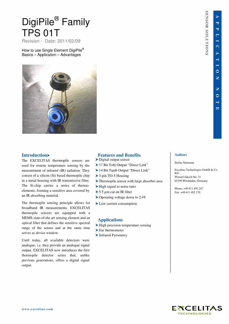
Introduction The EXCELITAS thermopile sensors are
used for remote temperature sensing by the
measurement of infrared (IR) radiation. They
consist of a silicon (Si) based thermopile chip
in a metal housing with IR transmissive filter.
The Si-chip carries a series of thermo-
elements, forming a sensitive area covered by
an IR absorbing material.
The thermopile sensing principle allows for
broadband IR measurements. EXCELITAS
thermopile sensors are equipped with a
MEMS state-of-the art sensing element and an
optical filter that defines the sensitive spectral
range of the sensor and at the same time
serves as device window.
Until today, all available detectors were
analogue, i.e. they provide an analogue signal
output. EXCELITAS now introduces the first
thermopile detector series that, unlike
previous generations, offers a digital signal
output.
Features and Benefits Digital output sensor
17 Bit Tobj Output “Direct Link”
14 Bit Tamb Output “Direct Link”
3-pin TO-5 Housing
Thermopile sensor with large absorber area
High signal to noise ratio
5.5 µm cut on IR filter
Operating voltage down to 2.4V
Low current consumption
Applications
High precision temperature sensing
Ear thermometer
Infrared Pyrometry
Authors
Stefan Naumann
Excelitas Technologies GmbH & Co.
KG.
Wenzel-Jaksch-Str. 31
65199 Wiesbaden, Germany
Phone: +49 611 492 247
Fax: +49 611 492 170
DigiPile® Family
TPS 01T Revision - Date: 2011/02/09 How to use Single Element DigiPile
®
Basics – Application – Advantages
SE
NS
OR
SO
LU
TIO
NS
A
PP
LI
CA
TI
ON
N
OT
E

w ww .exce l i ta s . co m TPS 0 1 T 2
AP
PL
IC
AT
IO
N
NO
TE
Table of Contents
1 Definitions................................................................................................. 3
2 Electrical Configuration.......................................................................... 3
2.1 From Analogue to Digital .................................................................................................. 3
2.2 The Digital Zero Signal Line ............................................................................................. 3
2.3 Data Communication ......................................................................................................... 4
2.4 Pull up/down current .......................................................................................................... 5
2.5 Direct Link interface Read Out .......................................................................................... 6
2.6 Electrical Data.................................................................................................................... 8
3 Software Filter Recommendation .......................................................... 9
4 Typical Application Circuit .................................................................... 9
5 Ambient Temperature Compensation ................................................... 9
6 Operating and Handling ....................................................................... 10
6.1 Handling .......................................................................................................................... 10
6.2 Soldering Conditions ....................................................................................................... 10
6.3 Product Safety & RoHS ................................................................................................... 10
6.4 Performance Advice......................................................................................................... 10
7 Frequently Asked Questions ................................................................. 11
List of Figures
Figure 1 Block diagram of DigiPile® ............................................................................................... 3
Figure 2 DigiPile® connections ........................................................................................................ 4
Figure 3 DigiPile® Data representation ............................................................................................ 4
Figure 5 DigiPile® read-out flow chart ............................................................................................. 6
Figure 6 DigiPile® read-out program example ................................................................................. 8
Figure 7 Typical application circuit ................................................................................................. 9
List of Tables
Table 1 DigiPile® electrical data ..................................................................................................... 8

w ww .exce l i ta s . co m TPS 0 1 T 3
AP
PL
IC
AT
IO
N
NO
TE
1 Definitions
Element: This is a sensing surface with a defined size. As all units work with optics, this element and the optics will
determine the performance.
Detector / Sensor: A detector gives a pure output signal; the sensor has a processed signal output.
Direct link interface: The direct link is the interface between DigiPile® and any micro controller. It is a bidirectional
single wire connection specially designed for this kind of application.
Data Rate: The refresh time of data (availability of new data block).
Resolution: The analogue value of one bit.
Clock Time: This refers to the n x (1 / internal clock frequency (the frequency of internal command processing)).
2 Electrical Configuration
The DigiPile® consists of a single element thermopile chip that is connected to a special integrated circuit. It
contains the analogue -to-digital converters that are generating 17-bit Tobj and 14 bit Tamb signals, a second-
order digital low-pass filter, an on-chip low-power oscillator, and a serial interface. The functional block
diagram is shown below.
Figure 1 Block diagram of DigiPile®
2.1 From Analogue to Digital
The DigiPile® is a Thermopile Sensor that displays information in “bit” as compared to mV signals of analogue
detectors. For engineers traditionally laying out systems in respect to analogue signals, the following rough
comparison may be helpful:
• Resolution: 1 count ≙ 0.8 µV
• Range: 0 to 130000 count ≙ ± 52.0 mV
• DC offset 64500 counts ≙ 0V typical
• Noise: ≈ 10 counts ≙ 8 µV (with low-pass)
2.2 The Digital Zero Signal Line
Due to the principle of thermopile temperature measurement, the thermopile voltage can be positive or negative
depending on if the object temperature is higher or lower than the ambient temperature. In order to allow signal
processing of negative voltages with a single supply system, the thermopile signal needs an electrical offset to
process the signals. The internal voltage reference provides this offset. To the user, this offset appears as a
digital zero line ranging at a value of 64500 (decimal) and may differ in series from one part to the next. To
recognize the zero line of the individual detector, the user may use either a digital band-pass or subtract the
measured offset from the signal. To do so, the detector must be covered from incidental radiation and protected
from possible air drafts and indirect radiations. The detector output is then monitored. The resulting signal
direct link
communication
(Single line
bi-directional
interface)
ADC Tobj
Decimator
&
Low Pass
Serial
Interface
Voltage
Reference
Decimator
&
Low Pass
Oscillator
ADC Tamb
direct link
VDD
VSS
TP
Power
Supply
w ww .exce l i ta s . co m TPS 0 1 T 4
AP
PL
IC
AT
IO
N
NO
TE
represents the individual zero line. Once the reading is stabilized, this value can be taken and stored in the
user’s µProcessor as the detector’s zero line.
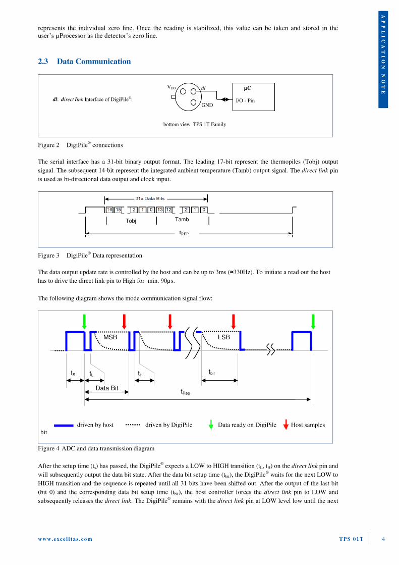
2.3 Data Communication
Figure 2 DigiPile® connections
The serial interface has a 31-bit binary output format. The leading 17-bit represent the thermopiles (Tobj) output
signal. The subsequent 14-bit represent the integrated ambient temperature (Tamb) output signal. The direct link pin
is used as bi-directional data output and clock input.
Figure 3 DigiPile® Data representation
The data output update rate is controlled by the host and can be up to 3ms (≈330Hz). To initiate a read out the host
has to drive the direct link pin to High for min. 90µs.
The following diagram shows the mode communication signal flow:
driven by host driven by DigiPile Data ready on DigiPile Host samples
bit
Figure 4 ADC and data transmission diagram
After the setup time (ts) has passed, the DigiPile® expects a LOW to HIGH transition (tL, tH) on the direct link pin and
will subsequently output the data bit state. After the data bit setup time (tbit), the DigiPile® waits for the next LOW to
HIGH transition and the sequence is repeated until all 31 bits have been shifted out. After the output of the last bit
(bit 0) and the corresponding data bit setup time (tbit), the host controller forces the direct link pin to LOW and
subsequently releases the direct link. The DigiPile® remains with the direct link pin at LOW level low until the next
dl: direct link Interface of DigiPile®: GND
bottom view TPS 1T Family
VDD
dl µC
I/O - Pin
Tobj Tamb
MSB LSB
tS tL tH tbit
Data Bit tRep
tREP
w ww .exce l i ta s . co m TPS 0 1 T 5
AP
PL
IC
AT
IO
N
NO
TE
signal sample read out is forced by the host or will change to HIGH level if read out rate (tREP) becomes slower
than15ms.
The data bit setup time tbit specified under electrical data is a minimum time. For the LOW level, it can vary
depending on the capacitive load of the direct link pin. It is recommended to start host interface implementation with
a longer data bit settling time tbit to ensure proper LOW level settling, reducing tbit empirically to optimize reliable
data transmission at maximum transmission speed. To avoid communication issues do not exceed the direct link Low
time.
If data transmission is interrupted during data clock low time (tL), the serial interface is updated with a new value,
provided tL lasts longer than the serial interface update time (tREP), which can cause a false reading if the data
transmission is continued. Therefore data transmission should preferable be interrupted during data clock high time
(tH). If interruption lasts longer than the serial interface update time (tREP), the serial interface will not be updated
with new values.
If a host reads the serial interface output faster than the maximum update rate of the serial interface (tREP), the data
bits are all read LOW.
2.4 Pull up/down current
Despite the fact that the direct link interface is designed is to be operated as input and as output, physically it is only
an output with limited current drive capabilities. This allows the host to overwrite the output by driving and sinking
the appropriate pull up and pull down currents.
When the data link pin drives HIGH level and the host forces low level, e.g. during data clock low time (tL) in order
to start readout sequence of the next bit, the host must be capable to sink the pull up current as specified, without
exceeding the maximum LOW level voltage.
When the data link pin drives LOW level and the host forces HIGH level, e.g. during data clock high time (tH), the
host must be capable to source the pull up current as specified, without falling below the minimum HIGH level
voltage.
Although the Pull up and Pull down currents exceed the maximum supply current considerably it becomes not
perceptible for the supply current, since it appears only during a very short time period while the host generates the
data clock. Therefore it is recommended to keep data clock low time (tL) and data clock high time (tH) as short as
possible in order to avoid unnecessary power consumption.
w ww .exce l i ta s . co m TPS 0 1 T 6
AP
PL
IC
AT
IO
N
NO
TE
2.5 Direct Link interface Read Out
Figure 5 DigiPile®
read-out flow chart
To transfer the above read-out flow chart into a software code, the following program code in C-language can be
applied. (Program code example for Microchip PIC 16 / PIC 18 family - as I/O- pin port B0 is used, CCS C
Compiler)
// DL: Direct Link Interface of the DigiPile®. A bidirectional single wire interface,
// directly connectable to most µC’s I/O- pins.
#TYPE LONG=32
#if defined(__PCM__) // if PIC 16 family is used
#include <16F886.h> // <=== type in the appropriate MC type here
#byte TrisReg_B=0x086 // <=== Look at datasheet for this value
#fuses INTRC_IO, NOWDT, NOPROTECT, NOLVP, NOBROWNOUT
#use delay(clock=8000000) // <=== type in the appropriate clock rate in Hz
#use rs232(baud=57600, xmit=PIN_C6, rcv=PIN_C7, stream=serial)
// ------ include files -------- ------------------------------------------------------------------------------------------------------
#include <stdlib.h>
#include <stdio.h>
#include <string.h>
Configure DL Pin as output
Set DL Port low for min. 200ns
Configure DL Port as output
Set DL Port High for min. 90µs
for (i=0; i < 14; i++)
Configure DL Port as output
Set DL Port low for min. 200ns
Set DL Port high for min. 200ns
Configure DL Port as input
Tamb << 1; shift bits left by 1 bit
if ( DL Port == high) Tamb++; // read 1
Configure DL Port as input
return()
Subroutine Read_DigiPile()
Clear data variables Tobj and Tamb
for (i=0; i <17; i++)
Configure DL Port as output
Set DL Port low for min. 200ns
Set DL Port high for min. 200ns
Configure DL Port as input
Tobj << 1; shift bits left by 1 bit
if ( DL Port == high) Tobj++; // read 1
Note: Make sure this routine is executed only once within 3 ms. Faster read out will cause false readings
w ww .exce l i ta s . co m TPS 0 1 T 7
AP
PL
IC
AT
IO
N
NO
TE
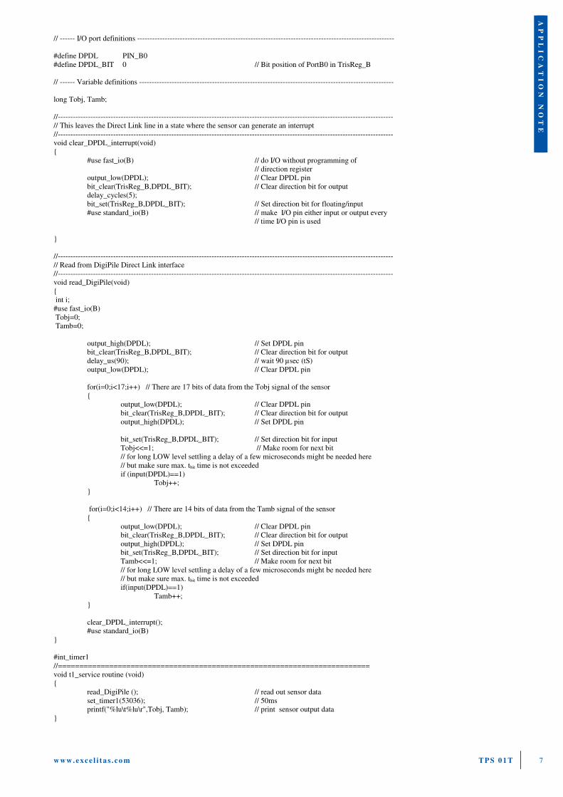
// ------ I/O port definitions ------------------------------------------------------------------------------------------------------
#define DPDL PIN_B0
#define DPDL_BIT 0 // Bit position of PortB0 in TrisReg_B
// ------ Variable definitions -----------------------------------------------------------------------------------------------------
long Tobj, Tamb;
//-------------------------------------------------------------------------------------------------------------------------------------
// This leaves the Direct Link line in a state where the sensor can generate an interrupt
//-------------------------------------------------------------------------------------------------------------------------------------
void clear_DPDL_interrupt(void)
#use fast_io(B) // do I/O without programming of
// direction register
output_low(DPDL); // Clear DPDL pin
bit_clear(TrisReg_B,DPDL_BIT); // Clear direction bit for output
delay_cycles(5);
bit_set(TrisReg_B,DPDL_BIT); // Set direction bit for floating/input
#use standard_io(B) // make I/O pin either input or output every
// time I/O pin is used
//-------------------------------------------------------------------------------------------------------------------------------------
// Read from DigiPile Direct Link interface
//-------------------------------------------------------------------------------------------------------------------------------------
void read_DigiPile(void)
int i;
#use fast_io(B)
Tobj=0;
Tamb=0;
output_high(DPDL); // Set DPDL pin
bit_clear(TrisReg_B,DPDL_BIT); // Clear direction bit for output
delay_us(90); // wait 90 µsec (tS)
output_low(DPDL); // Clear DPDL pin
for(i=0;i<17;i++) // There are 17 bits of data from the Tobj signal of the sensor
output_low(DPDL); // Clear DPDL pin
bit_clear(TrisReg_B,DPDL_BIT); // Clear direction bit for output
output_high(DPDL); // Set DPDL pin
bit_set(TrisReg_B,DPDL_BIT); // Set direction bit for input
Tobj<<=1; // Make room for next bit
// for long LOW level settling a delay of a few microseconds might be needed here
// but make sure max. tbit time is not exceeded
if (input(DPDL)==1)
Tobj++;
for(i=0;i<14;i++) // There are 14 bits of data from the Tamb signal of the sensor
output_low(DPDL); // Clear DPDL pin
bit_clear(TrisReg_B,DPDL_BIT); // Clear direction bit for output
output_high(DPDL); // Set DPDL pin
bit_set(TrisReg_B,DPDL_BIT); // Set direction bit for input
Tamb<<=1; // Make room for next bit
// for long LOW level settling a delay of a few microseconds might be needed here
// but make sure max. tbit time is not exceeded
if(input(DPDL)==1)
Tamb++;
clear_DPDL_interrupt();
#use standard_io(B)
#int_timer1
//=========================================================================
void t1_service routine (void)
read_DigiPile (); // read out sensor data
set_timer1(53036); // 50ms
printf("%lu\t%lu\r",Tobj, Tamb); // print sensor output data
w ww .exce l i ta s . co m TPS 0 1 T 8
AP
PL
IC
AT
IO
N
NO
TE
//=========================================================================
void main(void)
setup_timer_1(T1_INTERNAL | T1_DIV_BY_8); // Setup timer 1
enable_interrupts(INT_TIMER1);
enable_interrupts(GLOBAL);
port_b_pullups(FALSE); // disable Port B0 pull up resistor
clear_DPDL_interrupt();
while(1); // loop forever
Figure 6 DigiPile®
read-out program example
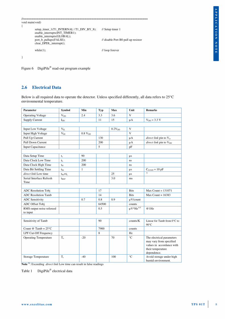
2.6 Electrical Data
Below is all required data to operate the detector. Unless specified differently, all data refers to 25°C
environmental temperature.
Parameter Symbol Min Typ Max Unit Remarks
Operating Voltage VDD 2.4 3.3 3.6 V
Supply Current IDD 11 15 µA VDD = 3.3 V
Input Low Voltage VIL 0.2VDD V
Input High Voltage VIH 0.8 VDD V
Pull Up Current 130 µA direct link pin to Vss
Pull Down Current 200 µA direct link pin to VDD
Input Capacitance 5 pF
Data Setup Time ts 90 µs
Data Clock Low Time tL 200 ns
Data Clock High Time tH 200 ns
Data Bit Settling Time tbit 1 µs CLOAD = 10 pF
direct link Low time tbit+tL 25 µs 1)
Serial Interface Refresh
Time
tREP 3.0 ms
ADC Resolution Tobj 17 Bits Max Count = 131071
ADC Resolution Tamb 14 Bits Max Count = 16383
ADC Sensitivity 0.7 0.8 0.9 µV/count
ADC Offset Tobj 64500 counts
RMS output noise refereed
to input
0.5 µV*Hz-0.5 @1Hz
Sensitivity of Tamb 90 counts/K Linear for Tamb from 0°C to
90°C
Count @ Tamb = 25°C 7900 counts
LPF Cut-Off Frequency 8 Hz
Operating Temperature To -20 70 °C The electrical parameters
may vary from specified
values in accordance with
their temperature
dependence.
Storage Temperature Ts -40 100 °C Avoid storage under high
humid environment.
Note 1): Exceeding direct link Low time can result in false readings
Table 1 DigiPile®
electrical data
w ww .exce l i ta s . co m TPS 0 1 T 9
AP
PL
IC
AT
IO
N
NO
TE
3 Software Filter Recommendation
The most unique feature of DigiPile® is the direct communication with the hosting microcontroller without requiring
any hardware filtering. Thus, it is recommended that software filters be implemented within the host.
Various websites give recommendations for software designed filters. You may also check at:
http://www-users.cs.york.ac.uk/~fisher/mkfilter/
http://www.atmel.com/dyn/resources/prod_documents/doc2527.pdf
Please note: The links above are to external websites and beyond EXCELITAS’s control or responsibility. For that
reason, EXCELITAS does not guarantee the accuracy of the content or any functions provided by these links.
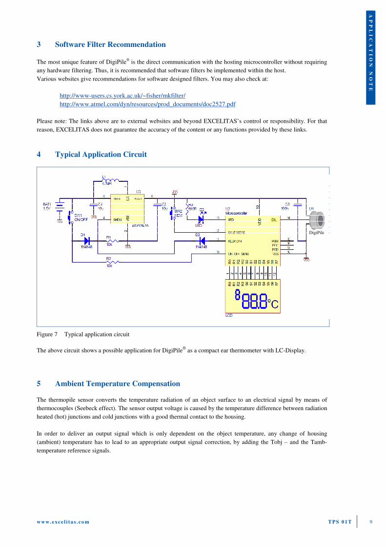
4 Typical Application Circuit
Figure 7 Typical application circuit
The above circuit shows a possible application for DigiPile®
as a compact ear thermometer with LC-Display.
5 Ambient Temperature Compensation
The thermopile sensor converts the temperature radiation of an object surface to an electrical signal by means of
thermocouples (Seebeck effect). The sensor output voltage is caused by the temperature difference between radiation
heated (hot) junctions and cold junctions with a good thermal contact to the housing.
In order to deliver an output signal which is only dependent on the object temperature, any change of housing
(ambient) temperature has to lead to an appropriate output signal correction, by adding the Tobj – and the Tamb-
temperature reference signals.
DigiPile
DL
w ww .exce l i ta s . co m TPS 0 1 T 1 0
AP
PL
IC
AT
IO
N
NO
TE
6 Operating and Handling
6.1 Handling Stresses above the absolute maximum ratings may cause damages to the device. Handle the detectors as ESD
sensitive devices and protect them from electrostatic discharges. Working areas should be conductive and grounded.
When handling detectors, operators must be grounded. Avoid mechanical stress on the housing and especially on the
leads. Be careful when cutting or bending leads to avoid damage. Do not bend leads less then 5 mm from their base.
Do not drop detectors on the floor. Do not expose the sensor to aggressive detergents such as Freon,
Trichloroethylene, etc. Avoid touching the detector window. To clean windows when necessary, use only ethyl
alcohol with a cotton swab.
6.2 Soldering Conditions For soldering the detectors within PCBs, the typically applied and recommended process is hand or wave soldering.
Hand soldering and wave soldering may be applied by a maximum temperature of 260°C for a dwell time less than
10 s. Avoid heat exposure to the top and the window of the detector. Reflow soldering is not recommended.
6.3 Product Safety & RoHS Modern high-tech materials are applied in the production of our Thermopile sensors. Some of these materials are
sensitive to high temperature exposure or to specific forms of stress. Our parts are compliant with environmental
regulations that may be reviewed on the EXCELITAS website. We recommend always checking your local
regulations. Disposal should only be carried out in accordance with the latest legislation and directives. In Europe,
WEEE directives must be followed. The Sensor fully complies with the European RoHS environmental directives
against the use of hazardous materials in electrical and electronic equipment.
6.4 Performance Advice Before taking a reading during testing, and/or operation, the unit must become thermally stable due to its nature as a
thermal detector and the high sensitivity of the device.
All data are specified at room temperature. When operating at other temperatures within the specified operating
range, parameters may vary. The detector might operate outside the quoted range, but may exhibit degraded
performance.
w ww .exce l i ta s . co m TPS 0 1 T 1 1
AP
PL
IC
AT
IO
N
NO
TE
7 Frequently Asked Questions
1. What is the data frame rate?
330Hz max.
2. Is the Thermopile output signal linear ?
No: The thermopile voltage shows a non-linear output characteristic versus the object temperature.
3. What is the Thermopile signal range?
Theoretically 0 to 131071. In the application it depends on the sensing range and the optical system.
4. Why do I have 64500 digits output with no radiation?
Digital offset / working point allows to measure below and above room temperature (25°C)
5. How often will the Master need to request a signal package? Is a 10 Hz sampling rate suitable?
The Master may repetitive request up to 330 times/s - one request = 1 package.
10 Hz may be sufficient with respect to the time constant and the LPF of the sensor. Higher data rates in
combination with averaging or low pass filtering may be of advantage for noise reduction.
6. Will I need signal filtering?
Filtering is not mandatory but may be of advantage for noise reduction.
7. Does the DigiPile® offer any cost saving advantages?
Yes, less component requirements, PCB space, and assembly work will result in lower system costs.
8. What is power supply requirement?
Minimum voltage requirement is 2.7 Volts, maximum supply current is 15 µA. As for any digital device,
the sensor may cause current peaks. Thus, a buffering capacitor of 100nF is recommended.
9. What are the advantages of DigiPile® compared to analogue version?
Thermopiles provide only very low voltage signals in the range of micro- to some milli-volts and have a
high output impedance. This makes them susceptible e.g. to RF disturbance. The DigiPile® output signal is
much more immune against RF. The signal does not need amplification and can be directly processed,
resulting in higher reliability for the complete system.
10. After power is applied how long before accurate readings can be obtained from the device?
a) The internal A/D- converter needs tREP = 3 ms to convert a value.
b) The detector has to reach thermal equilibrium with the environment. This can take a few seconds to
achieve accurate readings, which is typical for all thermal sensors.
11. What is the sampling rate?
Sampling rate is determined by the hosting µC and can be up to the specified refresh time of 3ms (≈ 1/330
Hz).
12. What is the content of a data package?
A data package consists of a ‘read data word’ signal (= high) initiated by the host. The microcontroller then
reads 17+14 bits. Data arrives with MSB first. The reading procedure is defined in chapter 2.3 data
communication.
13. How do I handle interrupts in data read out, without corrupting data?
The sensor only updates the data in the direct link interface, while it is at low level. There is no update if
direct link line is kept at high level.
If the controller has to serve an Interrupt, set the direct link line “high” for the duration of the interrupt.
When coming out of the interrupt routine, release it and read the value/bit. Continue reading as normal.
14. Output of the sensor: Is there a need for pull-up or may the sensor directly be hooked to the computer pin?
The DigiPile®
can be hooked directly to a digital I/O- pin of a microcontroller. But the µC must be able to
drive the pin to High and Low. With some µC's it might be necessary to have a pull-up resistor in the 25 kΩ
range, if the µC has problems to push the pin to High (the DigiPile®
input current is typ. 130 µA).
15. How to read the data output of TPS 1T Family by using a µC I/O port?
It should not be a problem to use an I/O- pin directly. The typical push/pull- current of the DigiPile®
is in
the range of 130 … 200 µA. This is enough for µC- input- impedance higher than 15kOhms. Please check
the output voltage with an oscilloscope. Does the voltage drop to Low too? If the DigiPile®
cannot produce
a High, a pull- up- resistor in the 15kOhm- range will help. But most likely it is a communication
problem/timing problem rather than a problem with the voltage levels.
16. Summary: The procedure to read the data from the DigiPile®
1. Drive the Direct Link interface high.
2. Then wait for 90 µs.
w ww .exce l i ta s . co m TPS 0 1 T 1 2
AP
PL
IC
AT
IO
N
NO
TE
3. Drive the line low for at least tL = 200 ns then pull it high for at least tH = 200 ns, then release it to read
(high impedance).
4. Then the detector will give the first bit (MSB) to the output.
5. Depending on your input capacitance, you have to wait with reading until there is a saturation of the
output (otherwise you will read a high)
6. Wait for at least tbit =1µs (for 10 pF on your input line, for higher C wait longer) to allow the line to
discharge your input capacitor.
7. Read the bit.
8. Repeat this (step 3 to 8) until all 17+14 data bits are read.
9. Then drive it low for at least tL = 200 ns, then release it (high impedance).
10. Wait minimum 2ms before reading the next value by repeating this procedure (steps 1 to 9) from the
start.
Excelitas GmbH & Co. KG.
Wenzel-Jaksch-Str. 31
65199 Wiesbaden, Germany
Telephone: (+49) 611-492-247
Fax: (+49) 611-492-170