digital combo multi-mode pfc and time-shift llc resonant
TRANSCRIPT

This is information on a product in full production.
March 2018 DocID030471 Rev 3 1/33
STNRG011
Digital combo multi-mode PFC and time-shift LLC resonantcontroller
Datasheet - production data
Features
Digital combo multi-mode PFC + time-shift LLC resonant half-bridge controller
Onboard 800 V startup circuit, line sense and X-cap discharge compliant with IEC 62368-1, for reduced standby power
Enhanced fixed on time multi-mode TM PFC controller with input voltage feedforward, THD optimizer and frequency limitation
Complete set of PFC protections
Time-shift control of resonant half-bridge
Enhanced burst-mode at light load with fast transient response and line adaptive half-bridge brown-out protection
Complete set of half-bridge protections
Available in SO20 package
Applications
Open frame SMPS
Flat screen TV SMPS
ATX power supply
AC-DC adapter
Figure 1. Block diagram
SO20
www.st.com

Contents STNRG011
2/33 DocID030471 Rev 3
Contents
1 Description . . . . . . . . . . . . . . . . . . . . . . . . . . . . . . . . . . . . . . . . . . . . . . . . . 5
2 Pin connection . . . . . . . . . . . . . . . . . . . . . . . . . . . . . . . . . . . . . . . . . . . . . . 6
3 Absolute maximum ratings and thermal data . . . . . . . . . . . . . . . . . . . . 7
4 Detailed block diagram . . . . . . . . . . . . . . . . . . . . . . . . . . . . . . . . . . . . . . . 8
5 Pin function . . . . . . . . . . . . . . . . . . . . . . . . . . . . . . . . . . . . . . . . . . . . . . . . 9
6 Electrical characteristics . . . . . . . . . . . . . . . . . . . . . . . . . . . . . . . . . . . . 11
7 Application schematics . . . . . . . . . . . . . . . . . . . . . . . . . . . . . . . . . . . . . 15
8 Architecture . . . . . . . . . . . . . . . . . . . . . . . . . . . . . . . . . . . . . . . . . . . . . . . 16
9 Functional description . . . . . . . . . . . . . . . . . . . . . . . . . . . . . . . . . . . . . . 18
9.1 HV startup and VCC management . . . . . . . . . . . . . . . . . . . . . . . . . . . . . . 18
9.2 AC line monitor and protection . . . . . . . . . . . . . . . . . . . . . . . . . . . . . . . . . 19
9.2.1 Brown-in/out . . . . . . . . . . . . . . . . . . . . . . . . . . . . . . . . . . . . . . . . . . . . . . 19
9.2.2 Line synchronization . . . . . . . . . . . . . . . . . . . . . . . . . . . . . . . . . . . . . . . 19
9.2.3 Line disconnection and X-cap discharge . . . . . . . . . . . . . . . . . . . . . . . . 19
9.2.4 Vline surge stop . . . . . . . . . . . . . . . . . . . . . . . . . . . . . . . . . . . . . . . . . . . 20
9.2.5 Line monitor for PFC control . . . . . . . . . . . . . . . . . . . . . . . . . . . . . . . . . 20
9.2.6 Early warning signal . . . . . . . . . . . . . . . . . . . . . . . . . . . . . . . . . . . . . . . . 20
9.3 Gate-drivers . . . . . . . . . . . . . . . . . . . . . . . . . . . . . . . . . . . . . . . . . . . . . . . 20
9.4 PFC control and fault management . . . . . . . . . . . . . . . . . . . . . . . . . . . . . 21
9.4.1 PFC resources . . . . . . . . . . . . . . . . . . . . . . . . . . . . . . . . . . . . . . . . . . . . 21
9.4.2 Vin reading . . . . . . . . . . . . . . . . . . . . . . . . . . . . . . . . . . . . . . . . . . . . . . . 21
9.4.3 PFC output voltage feedback reading . . . . . . . . . . . . . . . . . . . . . . . . . . 21
9.4.4 PFC OVP comparator . . . . . . . . . . . . . . . . . . . . . . . . . . . . . . . . . . . . . . 21
9.4.5 PFC RECOT comparator . . . . . . . . . . . . . . . . . . . . . . . . . . . . . . . . . . . . 21
9.4.6 PFC OC1 comparator . . . . . . . . . . . . . . . . . . . . . . . . . . . . . . . . . . . . . . 21
9.4.7 PFC OC2 comparator . . . . . . . . . . . . . . . . . . . . . . . . . . . . . . . . . . . . . . 22

DocID030471 Rev 3 3/33
STNRG011 Contents
33
9.4.8 PFC ZCD . . . . . . . . . . . . . . . . . . . . . . . . . . . . . . . . . . . . . . . . . . . . . . . . 22
9.4.9 PFC state machine event driven (SMED) . . . . . . . . . . . . . . . . . . . . . . . 22
9.5 PFC algorithm . . . . . . . . . . . . . . . . . . . . . . . . . . . . . . . . . . . . . . . . . . . . . 22
9.5.1 Ramp enhanced COT improved (patented) . . . . . . . . . . . . . . . . . . . . . . 22
9.5.2 Operating modes . . . . . . . . . . . . . . . . . . . . . . . . . . . . . . . . . . . . . . . . . . 23
9.6 PFC protections . . . . . . . . . . . . . . . . . . . . . . . . . . . . . . . . . . . . . . . . . . . . 23
9.6.1 PFC OVP . . . . . . . . . . . . . . . . . . . . . . . . . . . . . . . . . . . . . . . . . . . . . . . . 23
9.6.2 PFC OCP2 . . . . . . . . . . . . . . . . . . . . . . . . . . . . . . . . . . . . . . . . . . . . . . . 23
9.6.3 Surge . . . . . . . . . . . . . . . . . . . . . . . . . . . . . . . . . . . . . . . . . . . . . . . . . . . 23
9.6.4 PFC soft-start timeout . . . . . . . . . . . . . . . . . . . . . . . . . . . . . . . . . . . . . . 23
9.6.5 PFC UVP . . . . . . . . . . . . . . . . . . . . . . . . . . . . . . . . . . . . . . . . . . . . . . . . 23
9.6.6 PFC_FB disconnection . . . . . . . . . . . . . . . . . . . . . . . . . . . . . . . . . . . . . 24
9.6.7 PFC_CS disconnection . . . . . . . . . . . . . . . . . . . . . . . . . . . . . . . . . . . . . 24
9.6.8 PFC_ZCD disconnection . . . . . . . . . . . . . . . . . . . . . . . . . . . . . . . . . . . . 24
9.7 LLC control and fault management . . . . . . . . . . . . . . . . . . . . . . . . . . . . . 24
9.7.1 LLC related resources . . . . . . . . . . . . . . . . . . . . . . . . . . . . . . . . . . . . . . 24
9.7.2 LLC OC1 comparator . . . . . . . . . . . . . . . . . . . . . . . . . . . . . . . . . . . . . . . 24
9.7.3 LLC OC2 comparator . . . . . . . . . . . . . . . . . . . . . . . . . . . . . . . . . . . . . . . 25
9.7.4 LLC ZCD comparator . . . . . . . . . . . . . . . . . . . . . . . . . . . . . . . . . . . . . . . 25
9.7.5 LLC_FB voltage reading: OPTO feedback loop error . . . . . . . . . . . . . . 25
9.7.6 Shutdown feature . . . . . . . . . . . . . . . . . . . . . . . . . . . . . . . . . . . . . . . . . . 25
9.7.7 SMEDs . . . . . . . . . . . . . . . . . . . . . . . . . . . . . . . . . . . . . . . . . . . . . . . . . . 25
9.7.8 Algorithm . . . . . . . . . . . . . . . . . . . . . . . . . . . . . . . . . . . . . . . . . . . . . . . . 25
9.7.9 Time-shift (patented) . . . . . . . . . . . . . . . . . . . . . . . . . . . . . . . . . . . . . . . 25
9.8 LLC protections . . . . . . . . . . . . . . . . . . . . . . . . . . . . . . . . . . . . . . . . . . . . 26
9.8.1 Anti-capacitive protection . . . . . . . . . . . . . . . . . . . . . . . . . . . . . . . . . . . . 26
9.8.2 LLC OLP . . . . . . . . . . . . . . . . . . . . . . . . . . . . . . . . . . . . . . . . . . . . . . . . 26
9.8.3 LLC OCP2 . . . . . . . . . . . . . . . . . . . . . . . . . . . . . . . . . . . . . . . . . . . . . . . 26
9.8.4 LLC soft-start timeout . . . . . . . . . . . . . . . . . . . . . . . . . . . . . . . . . . . . . . . 26
9.8.5 LLC OVP . . . . . . . . . . . . . . . . . . . . . . . . . . . . . . . . . . . . . . . . . . . . . . . . 26
9.8.6 LLC_CS disconnection . . . . . . . . . . . . . . . . . . . . . . . . . . . . . . . . . . . . . 26
9.8.7 LLC_AUX disconnection . . . . . . . . . . . . . . . . . . . . . . . . . . . . . . . . . . . . 26
9.9 ADC . . . . . . . . . . . . . . . . . . . . . . . . . . . . . . . . . . . . . . . . . . . . . . . . . . . . . 27
9.10 Burst-mode . . . . . . . . . . . . . . . . . . . . . . . . . . . . . . . . . . . . . . . . . . . . . . . . 27
9.10.1 Specific resources . . . . . . . . . . . . . . . . . . . . . . . . . . . . . . . . . . . . . . . . . 27
9.10.2 Algorithm . . . . . . . . . . . . . . . . . . . . . . . . . . . . . . . . . . . . . . . . . . . . . . . . 27

Contents STNRG011
4/33 DocID030471 Rev 3
9.11 Communication and configuration . . . . . . . . . . . . . . . . . . . . . . . . . . . . . . 28
9.11.1 Monitor . . . . . . . . . . . . . . . . . . . . . . . . . . . . . . . . . . . . . . . . . . . . . . . . . . 29
9.11.2 Black box . . . . . . . . . . . . . . . . . . . . . . . . . . . . . . . . . . . . . . . . . . . . . . . . 29
9.11.3 Patches . . . . . . . . . . . . . . . . . . . . . . . . . . . . . . . . . . . . . . . . . . . . . . . . . 29
10 Package information . . . . . . . . . . . . . . . . . . . . . . . . . . . . . . . . . . . . . . . . 30
10.1 SO20 package information . . . . . . . . . . . . . . . . . . . . . . . . . . . . . . . . . . . . 30
11 Ordering information . . . . . . . . . . . . . . . . . . . . . . . . . . . . . . . . . . . . . . . 32
12 Revision history . . . . . . . . . . . . . . . . . . . . . . . . . . . . . . . . . . . . . . . . . . . 32
DocID030471 Rev 3 5/33
STNRG011 Description
33
1 Description
The STNRG011 embodies a multi-mode (transition-mode and DCM) PFC controller, a high-voltage double-ended controller for the LLC resonant half-bridge, an 800 V-rated startup generator and a sophisticated digital engine, that manage optimal operation of three blocks.
The device comes in a 20-pin SO package and offers an advanced solution for power-factor-corrected high-efficiency converters supposed to comply with the most stringent energy saving regulations.
The power system and the control algorithms are managed by an 8-bit core with dedicated fast peripherals (SMED). Optimized digital algorithms together with HW analog IPs are implemented to guarantee a very high performance, BOM optimization and robustness.
The digital algorithms are stored into an internal ROM memory and all key application parameters can be stored into a device's NVM (non-volatile memory) memory during the production phase allowing wide configurability and calibration.
The device can also externally communicate through a 2-pin UART, allowing the monitoring function, the black box storing into an external E2PROM and the software patch upload from the external E2PROM.
Pin connection STNRG011
6/33 DocID030471 Rev 3
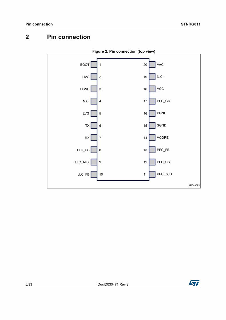
2 Pin connection
Figure 2. Pin connection (top view)

DocID030471 Rev 3 7/33
STNRG011 Absolute maximum ratings and thermal data
33
3 Absolute maximum ratings and thermal data
Table 1. Absolute maximum ratings
Symbol Pin Parameter Value Unit
VVAC VAC Voltage range -1 to 800 V
VBOOT BOOT Floating supply voltage, referred to GND -0.3 to 600 + VCC V
VFGND FGNDFloating ground voltage, connected to the half-bridge node
-3 up to a value included in the range BOOT - VCC and BOOT +0.3
V
dVFGND /dt FGND Floating ground max. slew rate 50 V/ns
VHVG HVG HVG voltage FGND -0.3 to BOOT +0.3 V
VVCC VCC IC supply voltage -0.3 to 19 V
VLVG
VPFC_GD LVG,
PFC_GDVoltage range -0.3 to VCC V
VVCORE VCORE Voltage range -0.3 to 5.5 V
IPFC_CS, ILLC_CS,
IPFC_ZCD,
PFC_CS, LLC_CS, PFC_ZCD
Clamped source current (pin voltage: < 0 V, self-limited)
2 mA
VPFC_CS, VLLC_CS, VPFC_ZCD
PFC_CS, LLC_CS, PFC_ZCD
Positive voltage range VCORE +0.3 V
VPFC_FB, VLLC_FB
PFC_FB. LLC_FB
Voltage range -0.3 to VCORE +0.3 V
VRX RX Voltage range -0.3 to VCORE +0.3 V
VTX TX Voltage range -0.3 to VCORE+ 0.3 V
Table 2. Thermal data
Symbol Parameter Value Unit
Rth j-amb Max. thermal resistance, junction to ambient 120 °C/W
Tj Junction temperature operating range -40 to 150 °C
Tstg Storage temperature -55 to 150 °C

Detailed block diagram STNRG011
8/33 DocID030471 Rev 3
4 Detailed block diagram
Figure 3. Detailed block diagram
DocID030471 Rev 3 9/33
STNRG011 Pin function
33
5 Pin function
Table 3. Pin function detailed description
No. Name Function
1 BOOT
High-side gate-drive floating supply voltage.
The bootstrap capacitor is connected between this pin and FGND.
A fast diode has to be connected from this pin and VCC to guarantee recharge of the bootstrap capacitor.
2 HVG
High-side gate-drive output.
The driver is capable of 0.5 A source and 0.75 A sink peak current (minimum values) to drive the upper MOSFET of the half-bridge leg.
A resistor internally connected to FGND ensures that the pin is never floating.
3 FGND
High-side gate-drive floating ground.
It is the return path for the high-side gate-drive current.
Layout carefully the connection of this pin to avoid too large spikes below ground.
4 N.C.High-voltage spacer.
The pin is not internally connected to isolate the high-voltage section and ease compliance with safety regulations (creepage distance) on the PCB.
5 LVG
Low-side gate-drive output.
The driver is capable of 0.5 A source and 0.75 A sink peak current (minimum values) to drive the lower MOSFET of the half-bridge leg.
The pin is actively pulled to GND during UVLO.
6 TX TX pin for UART/SDA pin for I2C interface
7 RX RX pin for UART/SCL pin for I2C interface
8 LLC_CS
LLC tank current sensing input. A voltage proportional to the tank current (usually obtained with a capacitive divider) has to be applied to this pin.
The information is used for zero-crossing detection (required by time-shift algorithm), the first and second level OCP.
9 LLC_AUXLLC_AUX is connected to a divider sensing the auxiliary voltage from the LLC transformer.
The LLC OVP detection is active on this pin.
10 LLC_FBThe voltage from this pin is used as the LLC feedback voltage. It has to be connected to the feedback phototransistor collector and a pull-up resistor to VCORE.
11 PFC_ZCDPFC ZCD input, connected to the PFC AUX winding through a resistor divider detecting the PFC inductor demagnetization.
12 PFC_CS
Current sense input for PFC.
The current flowing in the MOSFET is sensed through a resistor, and the resulting voltage is applied to this pin.
After GD turns on, a first voltage threshold cross allows enhanced COT control implementation.
A second level can be detected for overcurrent protection.
13 PFC_FBInput for PFC output voltage. It is used for closing the PFC loop and OVP protection. It has to be connected with a voltage divider to the bulk capacitor. If the early warning feature is enabled this pin is brought to 5 V when the EW pulse is released.
14 VCORE Internal VCORE bypass capacitor connection.

Pin function STNRG011
10/33 DocID030471 Rev 3
15 SGND Signal ground. Reference ground for analog signals.
16 PGNDPower ground. Current return for the PFC gate-driver and the low-side gate-driver of the half-bridge. Keep the PCB trace that goes from this pin to the sources of the PFC and the low-side MOSFETs separate from the trace that collects the grounding of the bias components.
17 PFC_GDPFC gate-driver output.
The output stage is able to drive power MOSFETs, it is capable of 0.7 A source current and 0.8 A sink current (minimum values).
18 VCC
Supply voltage of both the signal part of the IC and the gate-drivers. A bypass capacitor to GND is necessary to sustain the IC during startup and low power modes.
The voltage on the pin is internally clamped to protect the internal circuits from temporary excessive supply voltages.
19 N.C.The pin is not internally connected to isolate the high-voltage section and ease compliance with safety regulations (creepage distance) on the PCB.
20 VAC
High-voltage startup generator input.
The pin has to be connected directly to the mains voltage through two dedicated diodes.
If the voltage on the pin is higher than 50 V, an internal current source charges the capacitor connected between the pin VCC and GND until the voltage on the VCC pin reaches the startup threshold.
Normally, the generator is re-enabled when the voltage on the VCC pin falls below the UVLO threshold.
The pin is also used as the line voltage sensing input.
This pin is internally connected to a 20 M resistor divider. It is used for all line sense related functions: the AC brown-out, surge detection, line disconnection, input voltage feedforward, line synchronization.
When a line disconnection is detected, the internal current source is activated to discharge the X-capacitor.
Table 3. Pin function detailed description (continued)
No. Name Function

DocID030471 Rev 3 11/33
STNRG011 Electrical characteristics
33
6 Electrical characteristics
Tj = 0 to +125 °C, VCC = VBOOT = 15 V(a), CHVG = CLVG = CPFC_GD = 1 nF; unless otherwise specified.
a. Adjust VCC above VccOn before setting at 15 V.
Table 4. Electrical characteristics
Symbol Parameter Test condition Min. Typ. Max. Unit
Supply voltage
Vccz Vcc clamp voltage - 19 - - V
Vcc Operating range After turn-on 9.5 - 19 V
VccOn Processing turn-on threshold (1)Voltage rising 16 17 18 V
VccOff Processing turn-off threshold (1)Voltage falling 8 8.7 9.4 V
Hys Hysteresis - - 8.3 - V
VccCoreOn VCC threshold for VCore turn-on (1)Voltage rising - 8 - V
VccCoreOff VCC threshold for VCore turn-off (1)Voltage falling - 7 - V
VCore Operating range Isource 0 to 1 mA 4.75 - 5.25 V
Supply current
IVccs Quiescent current during sleep (BM)
T 25 °C - 0.5 - mA
IVccop
Operating supply current at fsw = 50 kHz, C = 1 nF, VCC = 12 V
PFC and LLC off - 18 -
mAPFC driver only (during PFC SS)
- 20 -
All drivers - 22 -
High-voltage startup generator
VVAC_BR Breakdown voltageIHV < 50 µA
VCC > VccOn800 - - V
IVAC_on ON-state VAC input current
VVAC > 40 V
VCC < 0.8 V- 1 -
mA
VVAC > 40 V
0.8 V < VCC < VccCoreOn- 6 -
VVAC > 100 V
VccCoreOn < VCC < 14 V- 6 -
VVAC > 100 V
14 V < VCC < VccOn- 4 -
40 V < VVAC < 100 V
VccCoreOn < VCC < 14 V- 20 -
40 V < VVAC < 100 V
14 V < VCC < VccOn- 10 -

Electrical characteristics STNRG011
12/33 DocID030471 Rev 3
IVcc_charge ON-state VCC charge current
VVAC > 40 V
VCC < 0.8 V-0.5 -0.75 -1
mA
VVAC > 40 V
0.8 V < VCC < VccCoreOn-3.5 -5 -7
VVAC > 100 V
VccCoreOn < VCC < 14 V- -5 -
VVAC > 100 V
14 V < VCC < VccOn- -3.5 -
40 V < VVAC < 100 V
VccCoreOn < VCC < 14 V- -18 -
40 V < VVAC < 100 V
14 V < VCC < VccOn- -8 -
IVAC_off OFF-state VAC input current VVAC = 400 V, VCC > VccOn - 20 40 µA
IVAC_HV_SINKVAC reading improvement current
VVAC = 100 V - 100 - µA
PFC - gate-driver
VOL Output low voltage Isink = 100 mA - - 0.7 V
VOH Output high voltage
Isource = -10 mA
VCC = 10 V,
VCC = 18 V
9.85
17.9
9.95
17.95
-
-
V
Isrcpk Peak source current Cgate = 4.7 nF(2) -0.7 -1.1 - A
Isnkpk Peak sink current Cgate = 4.7 nF(2) 0.8 1.3 - A
tf Voltage fall time - - 25 - ns
tr Voltage rise time - - 30 - ns
PFC_GD_uvlo UVLO saturation VCC = 0 to VccOn, Isink = 1 mA - 0.9 1.15 V
Low-side gate-driver (voltages referred to GND)
VOL Output low voltage Isink = 100 mA - - 0.7 V
VOH Output high voltage
Isource = -10 mA
VCC = 10 V
VCC = 18 V
9.85
17.85
9.9
17.9
-
-
V
Isrcpk Peak source current Cgate = 4.7 nF(2) -0.5 -0.8 - A
Isnkpk Peak sink current Cgate = 4.7 nF(2) 0.75 1.2 - A
tf Voltage fall time - - 25 - ns
tr Voltage rise time - - 40 - ns
LVG_uvlo UVLO saturation VCC = 0 to VccOn, Isink = 1 mA - 0.9 1.1 V
Table 4. Electrical characteristics (continued)
Symbol Parameter Test condition Min. Typ. Max. Unit

DocID030471 Rev 3 13/33
STNRG011 Electrical characteristics
33
High-side gate-driver (voltages referred to FGND)
VOL Output low voltage Isink = 100 mA - - 0.7 V
VOH Output high voltage
Isource = -10 mA
VBOOT= 10 V,
VBOOT = 18 V
9.85
17.85
9.9
17.9
-
-
V
Isrcpk Peak source current Cgate = 4.7 nF(2) -0.5 -0.8 - A
Isnkpk Peak sink current Cgate = 4.7 nF(2) 0.75 1.2 - A
tf Voltage fall time - - 25 - ns
tr Voltage rise time - - 40 - ns
HVG_pdw HVG-FGND pull-down resistor - - 25 - k
IFGND Current from VBOOT to FGND VBOOT = 200 V - 1.5 - A
X-CAP discharge
XCD_inact_time Inactivity detection time - - 50 - ms
IXCD Discharge current - 4 - - mA
Brown-in/out
BITH
Vline rising 112 114 116 V
BO Vline falling - 108 - V
BIBO_H HYST - 5.25 6 6.75 V
BO_mask Brown-out time - - 45 - ms
Overtemperature (by design)
OTPTH T rising 130 140 150 °CHYST T falling - -30 - °C
CK
Fck System clock in run mode - 57 60 63 MHz
ADC
ADC_res Resolution Vin ADC > 50 mV - 10 - bit
FSR_LConversion range
CS 0 - 1.5 V
FSR_H Other 0 - 2.5 V
DNL Differential non linearity Vin ADC > 50 mV - ±1.5 - lsb
Fck_ADC Clock frequency Vin ADC > 50 mV - 15 - MHz
Ts Sampling time Vin ADC > 50 mV - 7 -ADC Ck
cycles
Table 4. Electrical characteristics (continued)
Symbol Parameter Test condition Min. Typ. Max. Unit

Electrical characteristics STNRG011
14/33 DocID030471 Rev 3
TcTotal conversion time (sampling included)
Vin ADC > 50 mV - 18 -ADC Ck
cycles
Comparators
PFC_CS RECOT(3)TH RISING (DAC 6 bits)
Input pin PFC_CS
FSR = 125
STEP = 1.95 mV
HYST 5
PFC_CS OC1 TH RISING
Input pin PFC_CS- 500 -
mVTH FALLING - 450 -
PFC_CS OC2 TH RISING
Input pin PFC_CS- 900 -
mVTH FALLING - 850 -
PFC_ZCD ZCD(3)
TH FALLING (TH_F)
Input pin PFC_ZCD
0/50/100/200
mVTH RISING (TH_R)
210/110(4)/310/TH_F +10
PFC_FB OVPTH RISING
Input pin PFC_FB- 2.33 - V
HYST - 75 - mV
LLC_FB(3)
BURST
TH RISINGInput pin LLC_FB
0.75/1/1.25 V
HYST 5/10 mV
LLC_FB SHUTDOWN
TH RISING Input pin LLC_FB
- 145 -mV
TH FALLING - 125 -
LLC_AUX OVP TH RISING
Input pin LLC_AUX- 2.5 -
VTH FALLING - 2.4 -
LLC_AUX Ext. BMTH RISING
Input pin LLC_AUX- 0.9 -
VTH FALLING - 0.8 -
LINE SURGE TH RISING
Input pin VAC- 430 -
VTH FALLING - 410 -
LLC_CS OC1(3) TH RISING
Input pin LLC_CS
FSR = 500
STEP = 15.6 mV
HYST 20
LLC_CS OC2 TH RISING
Input pin LLC_CS- 700 -
mVTH FALLING - 650 -
1. Parameters tracking each other.
2. Guarantee by design, not production tested.
3. Thresholds and hysteresis are programmed by the software in use.
4. The selection for TH_R = 110 mV is not allowed if TH_F = 200 mV.
Table 4. Electrical characteristics (continued)
Symbol Parameter Test condition Min. Typ. Max. Unit
DocID030471 Rev 3 15/33
STNRG011 Application schematics
33
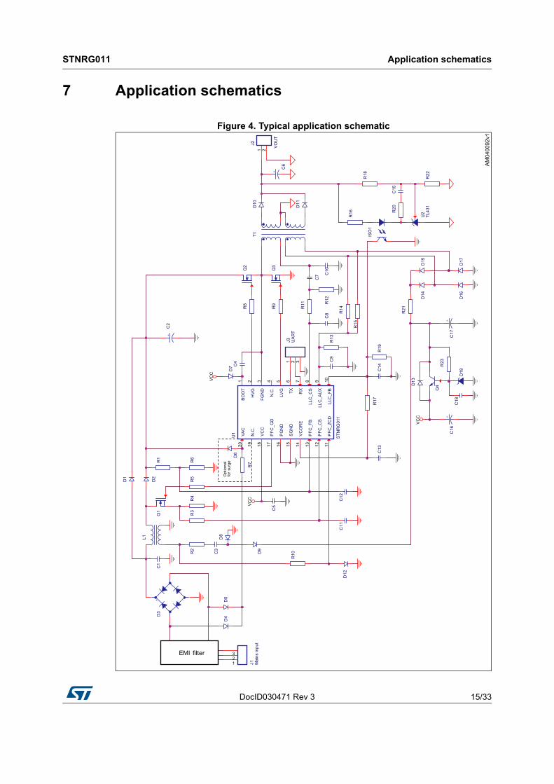
7 Application schematics
Figure 4. Typical application schematic
Architecture STNRG011
16/33 DocID030471 Rev 3
8 Architecture
The PFC and LLC external MOSFETs gates are managed by the “State Machine Event Driven” (SMEDs): 2 for PFC (PFC SMEDs) and 2 for LLC (LLC SMEDs).
The SMEDs are programmable state machine driven by events:
External events
– Analog comparators outputs
– Power manager generated events (protections)
Internal events
– Timers events
PFC SMEDs
Inputs events: PFC RECOT, PFC OC1, PFC ZCD
Outputs: PFC_GD
LLC SMEDs
Inputs events: LLC ZCD
Outputs: LVG, HVG
The µP subsystem manages dynamically the control loop.
Analog comparators thresholds setting
SMED configuration
SMED timers
ADC scheduler
Interrupt management
The multichannel ADC is controlled by a programmable event driven scheduler: sampling sequence can be configured and every sample can be triggered by a specific SMED state occurrence and an internal timer value. Different priorities can be programmed to allow fast sampling for real time control and slow sampling for state control (i.e. temperature).
The scheduler can be programmed to generate interrupts after completion of selectable conversions.
A dedicated AC line monitor easily follows the AC line providing system triggers.
The P reads data from the ADC and performs the loop calculation with the support of a dedicated 16-b x 16-b multiplier and a 32-b accumulator unit.
A Power management and burst-mode machine manages the system power state in order to have very low idle consumption and fast activity restart during the burst-mode operation.
Hard protections are managed with a very low propagation delay; the protection enable and the latched/not latched response are programmable.
The power manager controls also the brown-in/out, VCC charge/discharge, AC monitor and X-cap discharge.
A Watchdog resets the system in case of missed P signal for a long time.

DocID030471 Rev 3 17/33
STNRG011 Architecture
33
A communication peripheral allows serial communication at startup and during the normal operation for:
External memory communication for
– Black box external recording
– Patch SW upload
Monitoring
Internal memory R/W and OTP management
Test mode

Functional description STNRG011
18/33 DocID030471 Rev 3
9 Functional description
The main functions are:
HV startup and VCC management
Line monitor and protection
Drivers
PFC control and fault management
Resonant LLC HB control and fault management
Power management
Communication and configuration
9.1 HV startup and VCC management
The VAC pin voltage is a rectified sine wave at 100 Hz/120 Hz, connected to the mains AC line (Vline) through two dedicated diodes. The VAC pin is the device supply at the startup.
The VAC pin voltage is different from the PFC power path (Vin) where big caps are connected: the VAC pin partially follows the Vline also at no load condition while the Vin could be very close to a DC; this assumption allows to detect the AC line disconnection to implement the X-cap discharge function.
At the VAC pin a HV DMOS is internally connected to charge the capacitor connected to the VCC pin.
From the VCC pin an internal LDO provides the 5 V VCore for analog and digital circuitry; the digital section is supplied by the internal LDO from the VCORE pin.
At startup, from the HV DMOS the capacitor connected to the VCC pin is charged to provide the power supply to the whole device; then the HV DMOS is turned off.
The VCC pin starts sourcing current to the connected capacitor after a minimum 15 V VAC pin voltage.
The VCC capacitor charge current is limited to 0.75 mA during the first charge phase to limit the temperature increase in case the VCC pin is short-circuited at startup. After the VCC pin voltage is above 0.8 V, the charging current rises to 5 mA.
VCORE pin voltage rises when the VCC pin crosses 8 V (VccCoreOn). There is a VCORE overload protection that limits the VCC charging current below 1 mA in case the VCORE pin is short-circuited at startup. Then the VCC capacitor charge continues with an average current higher than 6 mA: the current is increased during the time the VAC pin voltage is below 100 V.
Once the VCC pin crosses the 17 V VccOn rising threshold the HV DMOS turns off and the whole device starts working: the P boots.
If the VCC pin goes below the 9 V VccOff falling threshold (UVLO threshold) the P stops working and the HV DMOS turns on again.

DocID030471 Rev 3 19/33
STNRG011 Functional description
33
If the VCC pin falls below 7 V (VccCoreOff) the device stops working and the capacitor connected to the VCORE pin discharges. The VCC pin can rise again only after the voltage on the VCORE pin falls below 1 V.
The worst case average charging current from the 0.8 V to the Vccon threshold is estimated in 4.63 mA and 4.11 mA, in case the mains voltage is 115 Vac - 60 Hz and 230 Vac - 50 Hz respectively.
9.2 AC line monitor and protection
A HV voltage divider is internally connected to the VAC pin to generate Vline_sense for the AC line monitoring and protection:
Brown-in/out
Line synchronization
Line disconnection and X-cap discharge
Surge detection and stop
Line monitor for PFC control
9.2.1 Brown-in/out
Brown-in and -out functions are implemented based on the Vline_sense information.
The peak VAC voltage is monitored to enable and disable the PFC.
The PFC is enabled when the AC line crosses the brown-in threshold. The PFC is disabled after 45 ms the AC line is below the brown-out threshold.
In order to improve AC line reading and avoid false brown-in, the HV DMOS is turned on sinking IXCD current for 100 ms in case of brown-out or line disconnection events. This function can be enabled / disabled through the dedicated NVM bit.
9.2.2 Line synchronization
A dedicated digital peripheral manages the PFC synchronization with the AC line sine wave.
In order to improve AC line reading and synchronization, the HV DMOS is turned on sinking IVAC_HV_SINK current at startup. This function can be enabled / disabled through the dedicated NVM bit.
9.2.3 Line disconnection and X-cap discharge
The Vline_sense is monitored to detect the AC line disconnection in order to discharge the X-cap through the internal HV DMOS.
The detection is based on AC activity absence on the VAC pin (the X-cap discharge function is triggered if there is no line activity for more than 50 ms). To discharge the X-cap, the HV DMOS turns on sinking a current of 4 mA minimum.
In order to improve AC line reading and avoid false brown-in, the HV DMOS is turned on sinking IXCD current for 100 ms in case of brown-out or line disconnection events. This function can be enabled / disabled through the dedicated NVM bit.
The discharge current stays on until the VAC pin is discharged or the AC line activity is detected again.
Functional description STNRG011
20/33 DocID030471 Rev 3
9.2.4 Vline surge stop
A surge can be detected on the VAC pin (430 V).
During the surge the PFC activity is stopped for one half-cycle.
If a line surge is detected during the PFC soft-start, the system shuts down with a not latched fault.
9.2.5 Line monitor for PFC control
A 20 M voltage divider for the AC line monitor is internally connected from the VAC pin to GND.
9.2.6 Early warning signal
In case a brown-out or another stopping event (early warning managed faults) is detected then the STNRG011:
Stops the PFC
LLC continues switching for about 5 ms, trying to keep the LLC output voltage regulated
PFC_FB pin is pulled up to VCore voltage for about 5 msec (early warning signal)
The early warning managed faults are
Brown-out
X-cap
PFC UVP
LLC OLP
If any other faults/events will occur, the STNRG011 will stop both PFC and LLC and will generate an early warning signal for about 250 sec.
The early warning signal generation is active as soon as the device starts driving the PFC MOSFET.
This function can be enabled / disabled through the dedicated NVM bit.
9.3 Gate-drivers
The HVG and LVG are matched drivers. Deadtimes are programmable by the user.
During the burst-mode sleep phase, the HS BOOT capacitor discharges. The burst packets always start with a LVG pulse to recharge the bootstrap capacitor. A fast external bootstrap diode is necessary.
DocID030471 Rev 3 21/33
STNRG011 Functional description
33
9.4 PFC control and fault management
9.4.1 PFC resources
9.4.2 Vin reading
Input line voltage peak (Vin) reading on the VAC pin by the ADC at the AC line peak.
9.4.3 PFC output voltage feedback reading
PFC output voltage reading on the PFC_FB pin by the ADC.
9.4.4 PFC OVP comparator
The PFC OVP comparator sets the limit for the PFC output voltage.
It monitors the PFC_FB pin with respect to a fixed 2.3 V threshold.
9.4.5 PFC RECOT comparator
The PFC RECOT comparator implements the TON adjustment for the ramp enhanced constant on-time (RECOT) control.
It monitors the PFC_CS pin with respect to a programmable threshold.
Its output communicates to the PFC SMED.
9.4.6 PFC OC1 comparator
The PFC OC1 comparator sets the limit for the operational maximum allowed peak current into the PFC MOSFET. If the OC1 threshold is hit the PFC_GD is turned off. This protection works cycle by cycle.
It monitors the PFC_CS pin with respect to a fixed 500 mV threshold.
Its output communicates to the PFC SMED.
Table 5. Related pins
Pin name Description Level Function
PFC_CS PFC MOSFET current sense
0 - 125 mV 6-bit ramp enhanced
COT feature
500 mV OCP1
900 mV OCP2 fault
PFC_ZCD PFC auxiliary connection for ZCD detection - -
PFC_FB Reading for PFC Vout estimation ADC, 10 bits -
VAC Mains line voltage reading ADC, 10 bits -
PFC_GD PFC MOSFET gate-driver - -

Functional description STNRG011
22/33 DocID030471 Rev 3
9.4.7 PFC OC2 comparator
The PFC OC2 comparator sets an HW limit for the current flowing into the PFC MOSFET: it triggers the OCP fault.
It monitors the PFC_CS pin with respect to a fixed 900 mV threshold.
9.4.8 PFC ZCD
The PFC ZCD comparator performs the zero cross detection to implement the soft switching of the PFC MOSFET.
It monitors the PFC_ZCD pin with respect to two programmable rising and falling thresholds.
Its output communicates to the PFC SMED.
9.4.9 PFC state machine event driven (SMED)
The PFC high frequency operations are managed by a programmable 8-state ”State Machine Event Driven” (2 coupled 4-state SMEDs).
The SMED controls the PFC MOSFET based on the PFC comparators output and internally controlled counters.
It generates also the comparators' enable signals.
It works at 60 MHz.
9.5 PFC algorithm
The PFC operates based on a multi-mode scheme.
A constant on-time (COT) control is implemented; TON is calculated from the PFC feedback and the measured Vin peak.
TON is calculated and updated at the line cycle valley.
Based on the working PFC's operating state variables the working mode is changed to optimize the overall efficiency.
9.5.1 Ramp enhanced COT improved (patented)
The PFC control is based on the constant on-time scheme, with a proprietary improved algorithm: the calculated TON is applied only after the PFC RECOT comparator is triggered to balance the recovery diode energy and the EMI capacitor current.
The PFC RECOT comparator threshold is adjusted by the core with a 6-bit DAC and allows to apply the programmed base and ramp (defined by user into NVM).
This feature allows improving the total harmonic distortion (THD) and the power factor (PF) of the application.

DocID030471 Rev 3 23/33
STNRG011 Functional description
33
9.5.2 Operating modes
The PFC manager changes the operating modes by dynamically reconfiguring the SMEDs, obtaining optimal performances in term of both efficiency and THD/PF.
Transition mode (TM mode)
Valley skipping
Discontinuous mode (DCM)
9.6 PFC protections
9.6.1 PFC OVP
In case the bulk voltage triggers the PFC OVP comparator, the system enters the fault state; the overvoltage protection can be programmed as latched or not latched.
The device implements also software overvoltage protection (SW OVP) that allows turning off the PFC until the next line valley in case the SW OVP threshold is reached. The SW OVP threshold is a NVM parameter.
9.6.2 PFC OCP2
If the PFC OC2 comparator is triggered, the PFC gate is truncated and remains off until the beginning of a new line half cycle. In case the PFC OC2 comparator is triggered for more than a programmable number of consecutives half line cycles the device enters the OCP2 fault and it is turned off.
The OCP2 fault can be programmed as latched or not latched.
9.6.3 Surge
When the surge comparator signal is high the PFC MOSFET is turned off and an interrupt is generated. The device will turn on the PFC MOSFET at the new line half cycle if the surge comparator output is low.
9.6.4 PFC soft-start timeout
If the PFC soft-start is not finished after 1 s the system enters the PFC soft-start timeout fault state and it is turned off. The fault is not latched.
9.6.5 PFC UVP
If the PFC_FB pin is below a threshold set by the user the device enters the PFC UVP fault and it is shut down. The system provides two different times of intervention configurable by NVM: adaptive and slow.
The slow intervention allows to shut off the system in case the UVP threshold is confirmed for at least 100 ms. The adaptive one allows to shut off the device immediately in case also the mains AC line is sensed below the brownout threshold for at least 1 half line cycle. On the contrary, the shut off will be delayed as if the intervention is set to slow, until the UVP and the mains conditions remain.

Functional description STNRG011
24/33 DocID030471 Rev 3
9.6.6 PFC_FB disconnection
If the PFC_FB is stuck low the system enters the PFC_FB disconnection fault state (latched) and it is turned off if the disconnection faults detection is enabled in NVM.
9.6.7 PFC_CS disconnection
If the PFC_CS pin is stuck low (or high) during the the PFC soft-start the system enters the PFC_CS disconnection fault state (latched) and it is shut down if the disconnection faults detection is enabled in NVM. In case the PFC_CS is stuck high during the operative mode the system enters the PFC_CS disconnection fault state and it is turned off if the disconnection faults detection is enabled in NVM.
9.6.8 PFC_ZCD disconnection
If the PFC_ZCD pin is stuck low or high during the the PFC soft-start the system enters the PFC_ZCD disconnection fault (latched) and it is turned off if the disconnection faults detection is enabled in NVM.
9.7 LLC control and fault management
9.7.1 LLC related resources
9.7.2 LLC OC1 comparator
The LLC OC1 comparator implements the overload protection (OLP). It monitors the LLC_CS pin with respect to a programmable threshold. If the LLC_CS pin goes every cycle over the OC1 threshold for a programmable time, the IC shuts down and enters the OLP fault.
Both threshold and duration are programmable trough NVM parameters.
Table 6. Pin
Pin name Description Level Function
LLC_CS Low-side current sense0 - 500 mV 5-bit OLP
700 mV OCP2 fault
LLC_AUX LLC auxiliary winding voltage sense0.9 V External burst-mode
2.5 V LLC output OVP
LLC_FBLLC OPTO feedback sense, burst comparator and SHUTDOWN comparator
ADC, 10 bits Feedback sense
Programmable Burst comparator
125 mV Shutdown comparator
HVG High-side gate driving - -
LVG Low-side gate driving - -

DocID030471 Rev 3 25/33
STNRG011 Functional description
33
9.7.3 LLC OC2 comparator
The LLC OC2 comparator sets an HW limit for the current flowing into the LLC resonant tank: it triggers the OCP2 fault.
It monitors the LLC_CS pin with respect to a fixed 700 mV threshold. If this threshold is triggered for a programmable consecutive number of cycles, the OCP2 fault is triggered and the system shuts down.
9.7.4 LLC ZCD comparator
The LLC ZCD comparator detects the LLC current zero-crossing during the normal operation to implement the time-shift control and the anti capacitive protection.
Its output communicates to the LLC SMED.
The comparator’s hysteresis is programmable by NVM choosing between the available values 5 mV or 10 mV.
9.7.5 LLC_FB voltage reading: OPTO feedback loop error
The LLC_FB pin is connected to the optocoupler and its voltage is the error signal of the LLC loop.
The LLC_FB voltage is sampled by the ADC to calculate the time-shift.
9.7.6 Shutdown feature
If the LLC_FB pin is forced below 125 mV, the device shuts down. If the voltage returns over such threshold the system restarts performing the soft-start.
This feature can be enabled / disabled using a NVM bit.
9.7.7 SMEDs
HVG and LVG are driven by an event driven 60 MHz state machine (2 coupled 4-state SMEDs).
Driving events are the ZCD event and the elapsing of the programmable time which sets the high-side and low-side time-shift values and drivers deadtime.
9.7.8 Algorithm
The LLC operation is based on “Symmetric Time-Shift Control” (STSC), an improved version of time-shift control that guarantees 50% of the HB duty cycle. The time-shift value is calculated from the LLC_FB pin.
9.7.9 Time-shift (patented)
The TSC methodology consists in controlling the amount of time elapsing from a zero-crossing of the tank current to the switch-off of the MOSFET currently on.
Conceptually, with TSC an inner loop is closed and the outer loop that regulates the output voltage provides the reference for the inner loop. This inner loop is completely managed by SMEDs using the zero current detection information.
Functional description STNRG011
26/33 DocID030471 Rev 3
9.8 LLC protections
9.8.1 Anti-capacitive protection
Anti-capacitive control is applied at the SMEDs level using ZCD time events.
The IC monitors the phase relationship between the LLC tank current sensed on the LLC_CS pin and the voltage at the HVG and LVG, checking the time between the gate rising edge and the tank current zero cross detection.
If this time is below a programmable threshold, which is indicative of impending the capacitive-mode operation, the monitoring circuit activates the “Soft” ACP procedure: the time-shift is reduced (and therefore the switching frequency is increased) in order to keep the converter away from that dangerous condition.
If the time reaches “zero” the device is stopped immediately. This is called “Hard” ACP.
Both hard and soft ACP can be enabled and disabled through NVM.
9.8.2 LLC OLP
If the LLC OC1 comparator is triggered the system could enter the overload protection (OLP). During this phase the system regulates the output and checks for a programmable time if the OCP1 event is still present, in this case the device is shut down entering the OLP fault state that can be programmed as latched or not latched.
9.8.3 LLC OCP2
If the LLC OC2 comparator is triggered for a number of times greater than a threshold set by the user the device sets the OCP2 fault and it is shut down. The OCP2 fault can be programmed as latched or not latched.
9.8.4 LLC soft-start timeout
If the LLC output voltage cannot reach the regulation value within 100 ms, the device enters the LLC soft-start timeout fault and it is shut down. The fault can be programmed as latched or not latched.
9.8.5 LLC OVP
If the LLC_AUX pin voltage is higher than the LLC OVP comparator threshold (2.5 V) the system enters the LLC OVP fault state and it is turned off. The fault can be programmed as latched or not latched and can be disabled.
9.8.6 LLC_CS disconnection
If the LLC_CS pin is stuck at 0 V or 5 V during the soft-start the system enters the LLC_CS disconnection fault (latched) and it is shut down if the disconnection faults detection is enabled in NVM.
9.8.7 LLC_AUX disconnection
If the pure external burst-mode is enabled and the LLC_AUX pin is stuck at 0 V during the burst and the LLC_FB pin is higher than the burst comparator threshold, after 32 burst

DocID030471 Rev 3 27/33
STNRG011 Functional description
33
packets the system enters LLC_AUX disconnection protection (latched) and it is shut down if the disconnection faults detection is enabled in NVM.
9.9 ADC
The system ADC is an 8-channel 15-MHz SAR 10-bit A/D converter.
It needs 7 cycles (470 ns) for sampling and 11 cycles (740 ns) to convert the data.
It is controlled by a SW programmable scheduler allowing flexible system signals reading:
Fixed time sequence conversion
Event driven sequence conversion
9.10 Burst-mode
9.10.1 Specific resources
Burst comparator on LLC_FB pin
The LLC BURST comparator at the LLC_FB pin is used to wake-up the system, in order to perform a burst sequence.
The comparator is alive also during sleep and the wake-up threshold is programmable (0.75 V, 1 V, 1.25 V).
External burst-mode comparator on LLC_AUX pin
The external burst-mode comparator with the 0.9 V threshold on the LLC_AUX pin is used to enter / exit the burst-mode using an external digital signal. The external burst-mode operation can be enabled / disabled using a NVM bit.
30-kHz system oscillator
A 30-kHz oscillator (always on) keeps the system alive.
9.10.2 Algorithm
The system can manage the deep sleep state with very low VCC current consumption (500 A).
Table 7. ADC input signals
Signal Pin Notes FSR
Input line voltage VAC Internal voltage divider 484.5 V
PFC feedback voltage PFC_FB Direct reading 2.5 V
LLC feedback voltage LLC_FB Direct reading 2.5 V

Functional description STNRG011
28/33 DocID030471 Rev 3
The system in deep sleep
Monitors the AC line for X-cap discharge and brown-out condition
Monitors the burst comparator to detect wake condition
Monitors the VCC for data integrity
All RAM data are maintained
The device implements two different burst-mode algorithms: the LLC_FB burst or external burst. The first one is based on just the LLC_FB pin voltage, the second one is based on the external BM comparator on the LLC_AUX pin that can be driven sensing the output current.
The burst-mode can be programmed to depends either on the LLC_FB pin only, or LLC_AUX pin only, or both. This third possibility is called hybrid external burst.
In case of the LLC_FB burst-mode, the device enters the sleep mode if the LLC_FB pin voltage goes below a programmable threshold. The burst switching activity is enabled after the burst comparator is triggered.
The normal switching activity is restored if the time between two bursts is lower than a programmable threshold. This time defines a precise power level at which the controller exits the burst-mode. In order to have a faster response to the big load transient the system exits the burst-mode also if the LLC_FB pin voltage is still above the burst comparator threshold after one burst packet.
In case of the LLC_AUX pin driven burst mode, two types of external burst mode could be defined:
Pure external burst mode: only the external BM comparator manages the burst mode entering / exiting;
Hybrid external burst mode: if the external BM comparator is high, the system stays out of burst mode while if the external BM comparator is low, burst mode entering / exiting is managed by the LLC_FB pin settings.
In both external burst mode cases, the burst switching activity is anyway managed by the LLC_FB pin and the burst comparator.
The PFC and LLC switching activities during the burst-mode are synchronized.
The LLC can perform a burst without the PFC, depending on the system conditions.
9.11 Communication and configuration
The device communicates with an external digital device through a serial interface.
The serial interface uses two dedicated pins with a standard UART protocol. It implements also an I2C protocol for external E2PROM writing and reading.
The serial interface allows the user
To write the NVM to configure the device in a specific application: 20 bytes are available.
To write into the RAM for test and SW patch purpose
To read the NVM content
To read the RAM content
To read registers content
To configure the device for specific tests

DocID030471 Rev 3 29/33
STNRG011 Functional description
33
Based on a specific code into the NVM the serial interface functionality can be reduced for security reasons.
9.11.1 Monitor
Some internal data can be provided to an external digital device trough the UART interface for monitoring purposes.
9.11.2 Black box
Black box data are written into the external E2PROM during the normal operation.
9.11.3 Patches
SW patches (if necessary) are uploaded by the device from the external E2PROM at the startup.
Maximum patch size is 2.5 kB.
Package information STNRG011
30/33 DocID030471 Rev 3
10 Package information
In order to meet environmental requirements, ST offers these devices in different grades of ECOPACK® packages, depending on their level of environmental compliance. ECOPACK specifications, grade definitions and product status are available at: www.st.com. ECOPACK is an ST trademark.
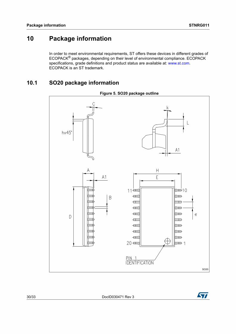
10.1 SO20 package information
Figure 5. SO20 package outline

DocID030471 Rev 3 31/33
STNRG011 Package information
33
Table 8. SO20 package mechanical data
Symbol
Dimensions
mm inch
Min. Typ. Max. Min. Typ. Max.
A 2.35 - 2.65 0.093 - 0.104
A1 0.10 - 0.30 0.004 - 0.012
B 0.33 - 0.51 0.013 - 0.020
C 0.23 - 0.32 0.009 - 0.013
D 12.60 - 13.00 0.496 - 0.512
E 7.40 - 7.60 0.291 - 0.299
e - 1.27 - - 0.050 -
H 10.00 - 10.65 0.394 - 0.419
h 0.25 - 0.75 0.010 - 0.030
L 0.40 - 1.27 0.016 - 0.050
K 0° (min.), 8° (max.)

Ordering information STNRG011
32/33 DocID030471 Rev 3
11 Ordering information
12 Revision history
Table 9. Order codes
Part number Package Packing
STNRG011 SO20 Tube
STNRG011TR SO20 Tape and reel
Table 10. Document revision history
Date Revision Changes
25-Oct-2017 1 Initial release.
15-Dec-2017 2Updated Figure 4: Typical application schematic on page 15 (replaced by new figure).
15-March-2018 3 Updated Table 9: Order codes on page 32.

DocID030471 Rev 3 33/33
STNRG011
33
IMPORTANT NOTICE – PLEASE READ CAREFULLY
STMicroelectronics NV and its subsidiaries (“ST”) reserve the right to make changes, corrections, enhancements, modifications, and improvements to ST products and/or to this document at any time without notice. Purchasers should obtain the latest relevant information on ST products before placing orders. ST products are sold pursuant to ST’s terms and conditions of sale in place at the time of order acknowledgement.
Purchasers are solely responsible for the choice, selection, and use of ST products and ST assumes no liability for application assistance or the design of Purchasers’ products.
No license, express or implied, to any intellectual property right is granted by ST herein.
Resale of ST products with provisions different from the information set forth herein shall void any warranty granted by ST for such product.
ST and the ST logo are trademarks of ST. All other product or service names are the property of their respective owners.
Information in this document supersedes and replaces information previously supplied in any prior versions of this document.
© 2018 STMicroelectronics – All rights reserved