digital control applications in power electronics lez3
TRANSCRIPT
October 1999 1Simone Buso - University of Padova - Lesson 3
LessonLesson 3 3
DigitalDigital Control of Three Control of Three--PhasePhase DC/AC DC/ACConvertersConverters:: Current Control Techniques Current Control Techniques
LinearLinear Current Control Current Control
October 1999 2Simone Buso - University of Padova - Lesson 3
Current SensingCurrent Sensing
•• Current sensingCurrent sensing is normally is normally notnot a a troublesome troublesomepart part of the control designof the control design.. Several solutions Several solutionscan be adoptedcan be adopted::
•• resistive shuntsresistive shunts;;
•• current transformerscurrent transformers;;
•• LEM (LEM (Hall effect basedHall effect based)) sensors sensors..
•• In In DC/DC converterDC/DC converter applications applications,, resistive resistiveshunts or current transformersshunts or current transformers,, if isolated if isolatedsensing is requiredsensing is required, are, are the the preferredpreferred,, cost cost--driven choicesdriven choices..
October 1999 3Simone Buso - University of Padova - Lesson 3
Current SensingCurrent Sensing
•• InIn VSI’s applicationsVSI’s applications ((suchsuch as as drives drives,, rectifiers rectifiers,,UPS’sUPS’s),), the cost of three the cost of three ((or two if the system hasor two if the system hasonly three wiresonly three wires)) Hall effect sensors is Hall effect sensors is normallynormallyreasonablereasonable..
•• This solution This solution greatly simplifiesgreatly simplifies the design of the the design of thecurrent control systemcurrent control system,, providing providing isolated andisolated andrelatively large bandwidthrelatively large bandwidth ( (≈≈≈≈ 100 kHz)100 kHz) current currentsensingsensing..
•• Only simple Only simple filteringfiltering ( (high frequency noisehigh frequency noise)) and andlevel adjusting circuitrylevel adjusting circuitry (to (to get get A/D converter A/D convertercompatible voltagecompatible voltage ranges) are ranges) are normally required normally required..
October 1999 4Simone Buso - University of Padova - Lesson 3
LinearLinear Current Control Current Control
•• The The simplestsimplest way of achieving way of achieving currentcurrentregulationregulation in in a DC/AC a DC/AC or or AC/DC AC/DC power powerconverterconverter is is to to employemploy linear linear regulators regulators((usually ofusually of PI PI type type).).
•• The The design anddesign and digital digital implementation implementation of such of suchregulators isregulators is quitequite straightforward straightforward and andnormally effectivenormally effective,, unless unless demanding staticdemanding staticand dynamicand dynamic performance performance specifications specifications are aregivengiven for for the current loop the current loop..
•• SomeSome basic guidelinesbasic guidelines can be given can be given for a for asuccesfull implementationsuccesfull implementation..
October 1999 5Simone Buso - University of Padova - Lesson 3
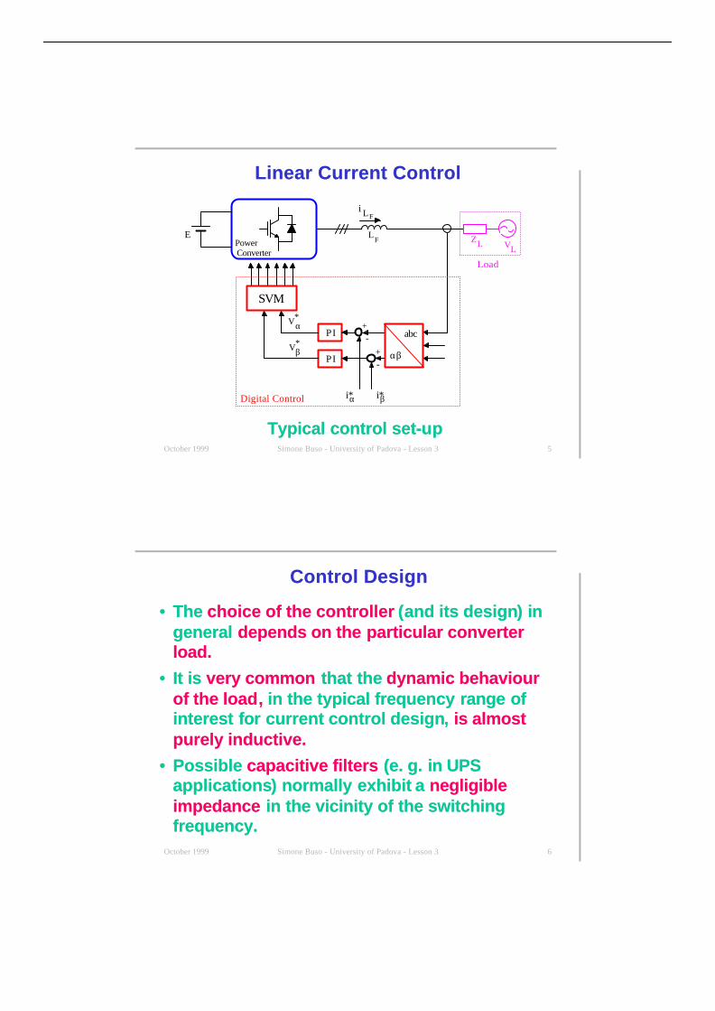
LF
abc
αβPI
PI
i* i*βα
SVM
E
+-
+-
PowerConverter
V*α
V*β
i LF
ZL VL
Load
Digital Control
LinearLinear Current Control Current Control
Typical control setTypical control set--upup
October 1999 6Simone Buso - University of Padova - Lesson 3
Control DesignControl Design
•• The The choice of the controllerchoice of the controller ( (and its designand its design)) in ingeneralgeneral depends on thedepends on the particular converter particular converterloadload..
•• It is It is very commonvery common that the that the dynamic behaviourdynamic behaviourof the loadof the load,, in the typical frequency in the typical frequency range range of ofinterestinterest for for current control design current control design,, is almostis almostpurely inductivepurely inductive..
•• Possible Possible capacitive filterscapacitive filters (e. g. (e. g. in in UPS UPSapplicationsapplications)) normally exhibit normally exhibit a a negligiblenegligibleimpedanceimpedance in the vicinity of the switching in the vicinity of the switchingfrequencyfrequency..

October 1999 7Simone Buso - University of Padova - Lesson 3
TypicalTypical Inverter Inverter Loads Loads
Can represent both aCan represent both adrivedrive or an or an active filteractive filterapplication or application or rectifierrectifier(with a (with a suitable suitable choice ofchoice ofthe the model parameters).model parameters).
Represents the typicalRepresents the typicalUPSUPS application. application.IILoadLoad
+LL RR
EE
LLCC
October 1999 8Simone Buso - University of Padova - Lesson 3
Design ExampleDesign Example
C = 100 C = 100 µµµµFF,, R = 0.1 R = 0.1 Ω,Ω,Ω,Ω, L = 2 L = 2 mHmH
VVdcdc = 400 V= 400 V ffswsw = 10 kHz= 10 kHz
LL RRCC IILoadLoad
VVdcdc/2/2
VVdcdc/2/2

October 1999 9Simone Buso - University of Padova - Lesson 3
TypicalTypical Inverter Inverter Loads Loads
Frequency (rad/sec)
Phas
e (d
eg);
Mag
nitu
de (
dB)
Bode Diagrams
0
20
40
60
80
103
104
105
106
0
50
100
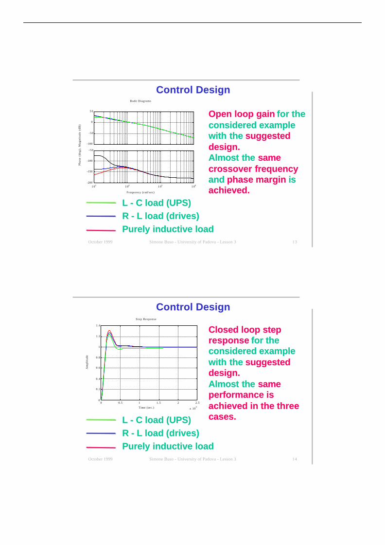
In the area around theIn the area around thepossible possible current loopcurrent loopcross-over frequencycross-over frequencythe inverter load isthe inverter load is‘seen’ as almost purely‘seen’ as almost purelyinductive.inductive.The controllerThe controller design designcan be verycan be very simple. simple.
L - C load L - C load (UPS)(UPS)R - L load R - L load (drives)(drives)Purely inductivePurely inductive load load
October 1999 10Simone Buso - University of Padova - Lesson 3
•• The The typically adoptedtypically adopted controller structure is the controller structure is theproportionalproportional-integral (PI).-integral (PI).
•• The The designdesign of the of the controller parameterscontroller parameters((proportional andproportional and integral integral gains gains)) isisstraightforward in the continousstraightforward in the continous time time domain domain..
•• The The discretizationdiscretization of the controller can be of the controller can beeasily easily performedperformed as as the the final final step step,, according according to toone of the various one of the various integration methodsintegration methods (e.g. (e.g.Euler orEuler or trapezoidal trapezoidal integration integration).).
•• There is There is normallynormally no no reason reason to to consider consider more moresofisticated approachessofisticated approaches..
Control DesignControl Design
October 1999 11Simone Buso - University of Padova - Lesson 3
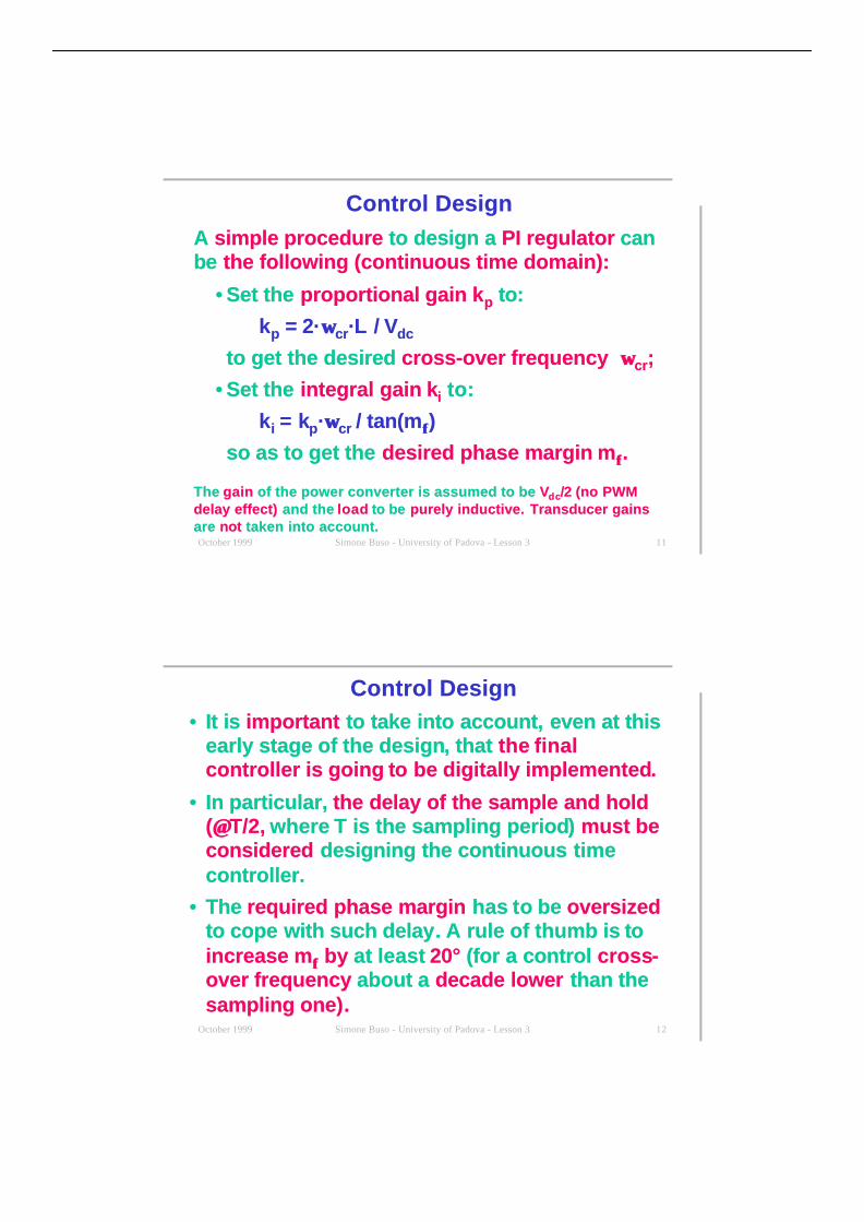
Control DesignControl DesignA A simple proceduresimple procedure to design a to design a PI regulator PI regulator cancanbebe the following (continuous time domain): the following (continuous time domain):
•• Set the Set the proportional gain proportional gain kkpp to: to:
kkpp = 2· = 2· ωωωωcrcr·L /·L / V Vdcdc
to get the desired to get the desired cross-over frequencycross-over frequency ωωωωcrcr;;
•• Set the Set the integral gain integral gain kkii to: to:
kkii = = kkpp··ωωωωcrcr / tan(/ tan(mmφφφφ))
so as to get the so as to get the desired phase margin desired phase margin mmφφφφ..
The The gaingain of the power converter is assumed to be of the power converter is assumed to be VVdcdc/2/2 (no PWM(no PWMdelay effect)delay effect) and the and the loadload to be to be purely inductive.purely inductive. Transducer gainsTransducer gainsare are notnot taken into account. taken into account.
October 1999 12Simone Buso - University of Padova - Lesson 3
Control DesignControl Design•• It is It is importantimportant to to take into account take into account,, even at this even at this
early stage of the designearly stage of the design,, that that thethe final finalcontroller is goingcontroller is going to to be digitally implemented be digitally implemented..
•• In particular,In particular, the delay of the sample and holdthe delay of the sample and hold((≅≅≅≅ T/2,T/2, wherewhere T T is the sampling period is the sampling period)) must bemust beconsideredconsidered designing the continuous designing the continuous time timecontrollercontroller..
•• The The required phase marginrequired phase margin has has to to be be oversizedoversizedto copeto cope with such delay with such delay. A. A rule of thumb is rule of thumb is to toincrease mincrease mφφφφ by by at leastat least 20° 20° (for a (for a control control crosscross--over frequency over frequency aboutabout a a decade lower decade lower than thethan thesampling onesampling one).).
October 1999 13Simone Buso - University of Padova - Lesson 3
Control DesignControl Design
Frequency (rad/sec)
Phas
e (d
eg);
Mag
nitu
de (
dB)
Bode Diagrams
-100
-50
0
5 0
1 03 1 04 1 05 1 06-200
-150
-100
-50
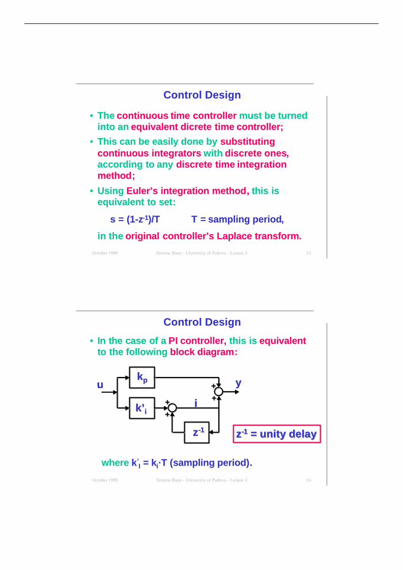
L - C load (UPS)L - C load (UPS)R - L load (drives)R - L load (drives)Purely inductive loadPurely inductive load
Open loop gainOpen loop gain for the for theconsidered exampleconsidered examplewith the with the suggestedsuggesteddesign.design.Almost theAlmost the same samecrossover frequencycrossover frequencyand and phase margin phase margin isisachieved.achieved.
October 1999 14Simone Buso - University of Padova - Lesson 3
Control DesignControl Design
Time (sec.)
Am
plit
ude
S tep Response
0 0.5 1 1.5 2 2.5
x 10-3
0
0.2
0.4
0.6
0.8
1
1.2
1.4
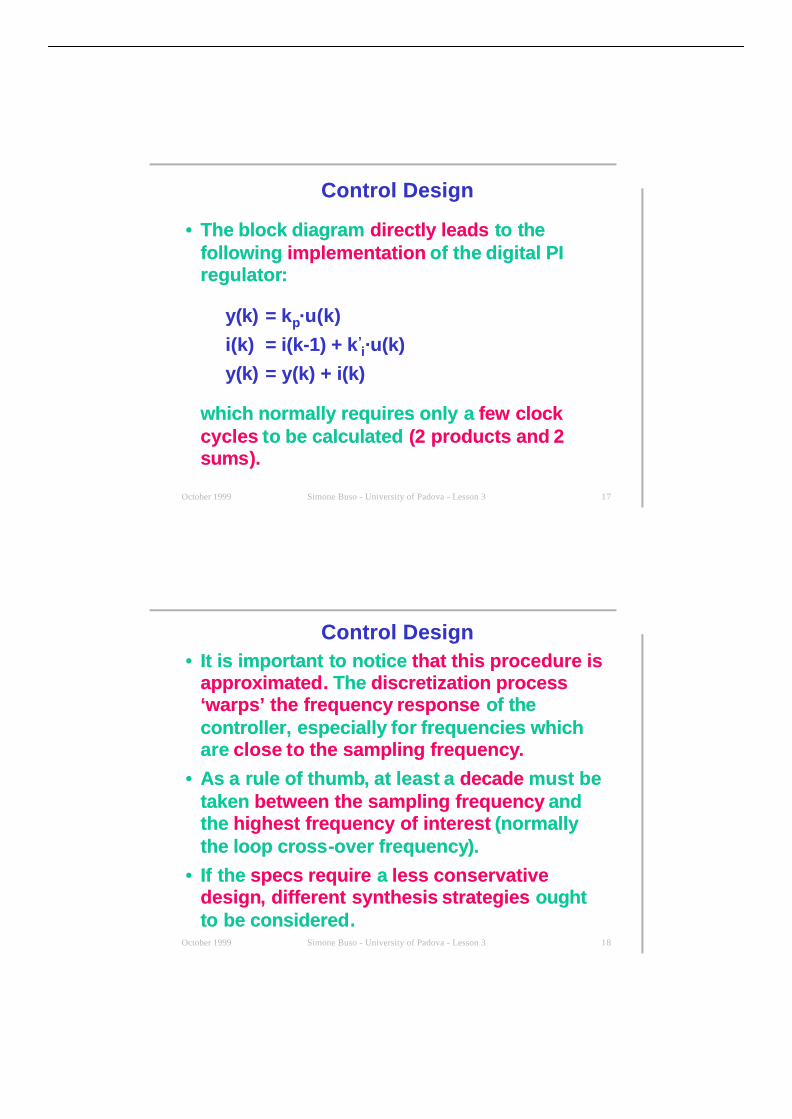
L - C load (UPS)L - C load (UPS)R - L load (drives)R - L load (drives)Purely inductive loadPurely inductive load
Closed loop stepClosed loop stepresponseresponse for the for theconsidered exampleconsidered examplewith the with the suggestedsuggesteddesign.design.Almost theAlmost the same sameperformance isperformance isachieved in the threeachieved in the threecases.cases.
October 1999 15Simone Buso - University of Padova - Lesson 3
Control DesignControl Design
•• TheThe continuous continuous time time controller controller must be turnedmust be turnedinto aninto an equivalent dicrete equivalent dicrete time time controller controller;;
•• This can be easily done byThis can be easily done by substituting substitutingcontinuous integrators continuous integrators withwith discrete ones discrete ones,,accordingaccording to to any any discrete discrete time time integration integrationmethodmethod;;
•• Using Using Euler’s integration methodEuler’s integration method,, this isthis isequivalentequivalent to to set set::
s = (1-zs = (1-z-1-1)/T)/T T =T = sampling period sampling period,,
in thein the original original controller’s Laplace transform controller’s Laplace transform..
October 1999 16Simone Buso - University of Padova - Lesson 3
Control DesignControl Design
•• InIn the the case case of of a a PIPI controller controller,, this is this is equivalentequivalenttoto the following the following block diagramblock diagram::
where where kk’’II = = k kii·T (·T (sampling periodsampling period).).
z-1 = unity delayzz-1-1 = unity delay = unity delay
+++
+++
++++++
kpkkpp
k’ik’k’ii
z-1zz-1-1
uuu yyy
iii
October 1999 17Simone Buso - University of Padova - Lesson 3
Control DesignControl Design
•• The block diagram The block diagram directly leadsdirectly leads to to the thefollowing following implementationimplementation of the of the digital PI digital PIregulatorregulator::
y(k)y(k) == k kpp·u(k)·u(k)
i(k)i(k) = i(k-1) += i(k-1) + k k’’ii·u(k)·u(k)
y(k)y(k) = y(k) + i(k)= y(k) + i(k)
which normally requires onlywhich normally requires only a a few clockfew clockcyclescycles to to be calculated be calculated (2(2 products and products and 2 2sumssums).).
October 1999 18Simone Buso - University of Padova - Lesson 3
Control DesignControl Design•• It is importantIt is important to to notice notice that this procedure isthat this procedure is
approximatedapproximated.. The The discretization processdiscretization process‘‘warps’ the frequencywarps’ the frequency response response of the of thecontrollercontroller,, especially especially for for frequencies which frequencies whichareare closeclose to to the sampling frequency the sampling frequency..
•• As aAs a rule of thumb rule of thumb,, at least at least a a decade decade must bemust betaken taken between the sampling frequencybetween the sampling frequency and andthe the highest frequency of interesthighest frequency of interest ( (normallynormallythe loop crossthe loop cross--over frequencyover frequency).).
•• If the If the specs requirespecs require aa less conservative less conservativedesigndesign,, different synthesisdifferent synthesis strategiesstrategies ought oughttoto be considered be considered..
October 1999 19Simone Buso - University of Padova - Lesson 3
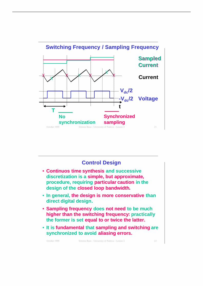
Switching FrequencySwitching Frequency / / Sampling Frequency Sampling Frequency
•• The The current waveformscurrent waveforms in VSI’s exhibit in VSI’s exhibit a asignificant significant high frequency harmonic contenthigh frequency harmonic contentduedue to to the the PWM PWM modulation modulation ((rippleripple).).
•• The The current control loopcurrent control loop is normally needed is normally needed to tocontrol the control the average valueaverage value of the converter’s of the converter’scurrentscurrents..
•• Sampling at Sampling at very high frequenciesvery high frequencies to toreconstruct thereconstruct the completecomplete current waveform current waveform((including the rippleincluding the ripple)) is therefore is therefore notnotnecessarynecessary..
October 1999 20Simone Buso - University of Padova - Lesson 3
Switching FrequencySwitching Frequency / / Sampling Frequency Sampling Frequency
•• On the other handOn the other hand,, sampling at highsampling at highfrequencies increasesfrequencies increases the achievable the achievable currentcurrentloop bandwidthloop bandwidth..
•• ThereforeTherefore, a, a simple or doublesimple or double sampling sampling per permodulation period is modulation period is normally adoptednormally adopted..
•• The basic idea is thatThe basic idea is that sampling and switching sampling and switchingmust bemust be synchronized synchronized toto avoid avoid errors errors..
•• CurrentsCurrents areare typically typically sampled at the sampled at thebeginning and in the middle beginning and in the middle of the modulationof the modulationperiodperiod..
October 1999 21Simone Buso - University of Padova - Lesson 3
Switching FrequencySwitching Frequency / / Sampling Frequency Sampling Frequency
TTSynchronizedSynchronizedsamplingsampling
NoNosynchronizationsynchronization
VoltageVoltage
CurrentCurrent
SampledCurrentSampledCurrent
tt--VVdcdc/2/2
VVdcdc/2/2
October 1999 22Simone Buso - University of Padova - Lesson 3
Control DesignControl Design
•• ContinuosContinuos time time synthesis synthesis and successive and successivediscretization isdiscretization is a a simplesimple,, but approximate but approximate,,procedureprocedure,, requiring requiring particularparticular caution caution in the in thedesign of the design of the closed loop bandwidthclosed loop bandwidth..
•• In general,In general, the design is the design is more more conservative conservative thanthandirectdirect digital digital design design..
•• Sampling frequencySampling frequency does does not neednot need to to be much be muchhigher than the switching frequencyhigher than the switching frequency:: practically practicallythe former is set the former is set equalequal to to or twice the latter or twice the latter..
•• It isIt is fundamentalfundamental that that sampling and switchingsampling and switching are aresynchronizedsynchronized to to avoid avoid aliasing errorsaliasing errors..

October 1999 23Simone Buso - University of Padova - Lesson 3
3 3.5 4 4.5 5 5.5 6 6.5 7 7.5 8
x 10-3
-30
-20
-10
0
10
20
30
Control DesignControl DesignTime domain simulation with PWM modulationTime domain simulation with PWM modulation
The controller’sThe controller’sresponse is goodresponse is goodbut somebut someovershootovershoot is isvisible at the endvisible at the endof of saturated modesaturated modeof operation.of operation.This can beThis can beimproved byimproved by anti antiwind-upwind-upimplementation.implementation.
October 1999 24Simone Buso - University of Padova - Lesson 3
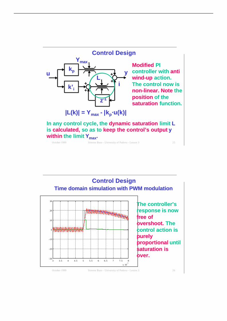
Control DesignControl Design
•• The The overshootovershoot is due is due to to the the integralintegral part part of the of thecontrollercontroller,, which gets which gets ““overchargedovercharged”” during duringthe saturated modethe saturated mode of operation of operation.. This has This has nonorelationrelation with the open loop with the open loop phase marginphase margin..
•• As aAs a consequence consequence, a, a negativenegative error error will be will beneededneeded to to removeremove the accumulated the accumulated positivepositiveerror.error. This generates the overshoot This generates the overshoot..
•• AA good good solutionsolution to to this problem is the so this problem is the so--calledcalledanti windanti wind--up actionup action..
•• This basically consists in theThis basically consists in the dynamic dynamicsaturation of thesaturation of the integral integral part part of the controllerof the controller..
October 1999 25Simone Buso - University of Padova - Lesson 3
Control DesignControl Design
In any control cycle, the In any control cycle, the dynamic saturationdynamic saturation limit limit LLis is calculated,calculated, so as to so as to keep the control’s outputkeep the control’s output yywithinwithin the limit the limit YYmaxmax..
|L(k)| = |L(k)| = YYmaxmax - |- |kkpp·u(k)|·u(k)|
ModifiedModified PI PIcontroller with controller with antiantiwind-upwind-up action. action.The control now isThe control now isnon-linear. Note non-linear. Note thetheposition position of theof thesaturation saturation function.function.
++++
++++
kkpp
k’k’ii
zz-1-1
uu yy
iiLL
YYmaxmax
October 1999 26Simone Buso - University of Padova - Lesson 3
3 3.5 4 4.5 5 5.5 6 6.5 7 7.5 8
x 10-3
-30
-20
-10
0
10
20
30
Control DesignControl DesignTime domain simulation with PWM modulationTime domain simulation with PWM modulation
The controller’sThe controller’sresponse is nowresponse is nowfree offree ofovershoot.overshoot. The Thecontrol action iscontrol action ispurelypurelyproportionalproportional until untilsaturation issaturation isover.over.
October 1999 27Simone Buso - University of Padova - Lesson 3
Three Phase ImplementationThree Phase Implementation
•• The control of The control of threethree--phase VSI’sphase VSI’s requires requires,, in ingeneral,general, three indipendentthree indipendent,, but normally but normallyidenticalidentical,, current controllers current controllers..
•• If theIf the neutralneutral is not connected is not connected,, currents currents are are notnotindipendentindipendent,, and therefore it is possible and therefore it is possible to tocontrol only control only two currents out of threetwo currents out of three..
•• It is therefore It is therefore also possiblealso possible to: to:
üü useuse Park’s transformationPark’s transformation to move to move from the from thea,a, b, c b, c toto thethe αααα, , ββββ fixed reference frame fixed reference frame;;
üü use use d, qd, q rotating reference frame rotating reference frame..
October 1999 28Simone Buso - University of Padova - Lesson 3
Three Phase ImplementationThree Phase Implementation
•• TheThe use use of of d, qd, q rotating reference rotating reference frame is frame is quite quitecommoncommon in adjustable speed in adjustable speed drive applicationsdrive applicationstoto simplify the dynamics of the electricalsimplify the dynamics of the electricalmachinemachine..
•• It can also be used in It can also be used in rectifierrectifier, UPS, UPS or active or activefilter applications of VSI’sfilter applications of VSI’s.. The advantage is the The advantage is thepossibility of possibility of controlling very preciselycontrolling very precisely the thefundamentalfundamental component component of any variable of any variable..
•• InIn any any case, case, the the d, qd, q transformation modifies transformation modifiesthe the dynamic equationsdynamic equations of the system of the system.. This Thismust be consideredmust be considered in the controller’s design in the controller’s design..
October 1999 29Simone Buso - University of Padova - Lesson 3
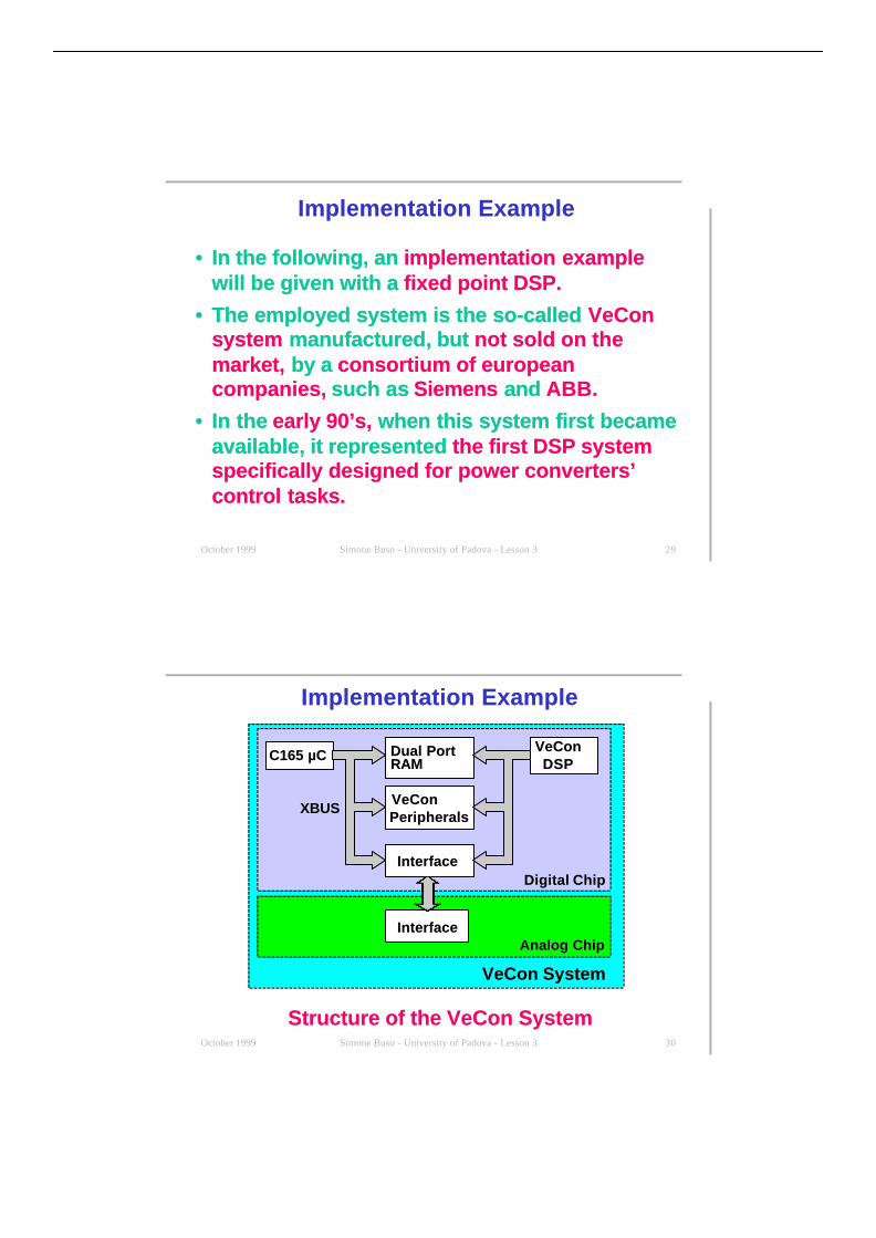
Implementation ExampleImplementation Example
•• In the following, an In the following, an implementation exampleimplementation examplewill be given with a will be given with a fixed point DSP.fixed point DSP.
•• The employed system is the so-calledThe employed system is the so-called VeConVeConsystemsystem manufactured, but manufactured, but not sold on thenot sold on themarket,market, by a by a consortium of europeanconsortium of europeancompanies,companies, such as such as SiemensSiemens and and ABB.ABB.
•• In the In the early 90’s,early 90’s, when this system first became when this system first becameavailable, it represented available, it represented the first DSP systemthe first DSP systemspecifically designed for power converters’specifically designed for power converters’control tasks.control tasks.
October 1999 30Simone Buso - University of Padova - Lesson 3
Dual PortDual PortRAMRAM
C165 µCC165 µCVeConVeConDSPDSP
Analog ChipAnalog Chip
VeConVeConPeripheralsPeripherals
XBUSXBUS
InterfaceInterface
InterfaceInterface
Digital ChipDigital Chip
VeConVeCon System System
Implementation ExampleImplementation Example
Structure of the Structure of the VeCon VeCon SystemSystem
October 1999 31Simone Buso - University of Padova - Lesson 3
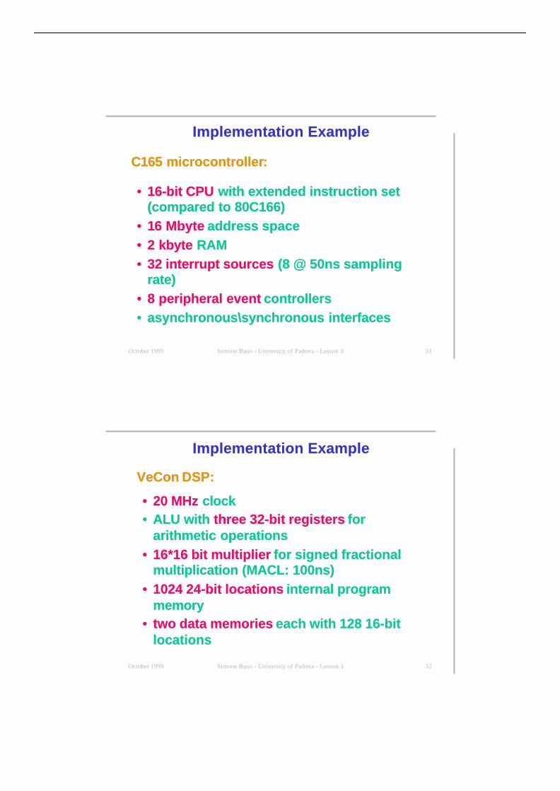
•• 16-bit CPU16-bit CPU with extended instruction set with extended instruction set(compared to 80C166)(compared to 80C166)
•• 1616 Mbyte Mbyte address space address space•• 22 kbyte kbyte RAM RAM•• 32 interrupt sources32 interrupt sources (8 @ 50ns sampling (8 @ 50ns sampling
rate)rate)•• 8 peripheral event8 peripheral event controllers controllers•• asynchronous\synchronous interfacesasynchronous\synchronous interfaces
C165C165 microcontroller microcontroller::
Implementation ExampleImplementation Example
October 1999 32Simone Buso - University of Padova - Lesson 3
Implementation ExampleImplementation Example
•• 20 MHz20 MHz clock clock•• ALU with ALU with three 32-bit registersthree 32-bit registers for for
arithmetic operationsarithmetic operations•• 16*16 bit multiplier16*16 bit multiplier for signed fractional for signed fractional
multiplication (MACL: 100ns)multiplication (MACL: 100ns)•• 1024 24-bit locations1024 24-bit locations internal program internal program
memorymemory•• two data memoriestwo data memories each with 128 16-bit each with 128 16-bit
locationslocations
VeConVeCon DSP: DSP:

October 1999 33Simone Buso - University of Padova - Lesson 3
•• Position sensorPosition sensor evaluation evaluation•• Inverter triggering Inverter triggering (PWM)(PWM)•• Interface to Interface to Analog ChipAnalog Chip•• Synchronous serial interfaceSynchronous serial interface
Peripheral Units:Peripheral Units:
Implementation ExampleImplementation Example
October 1999 34Simone Buso - University of Padova - Lesson 3
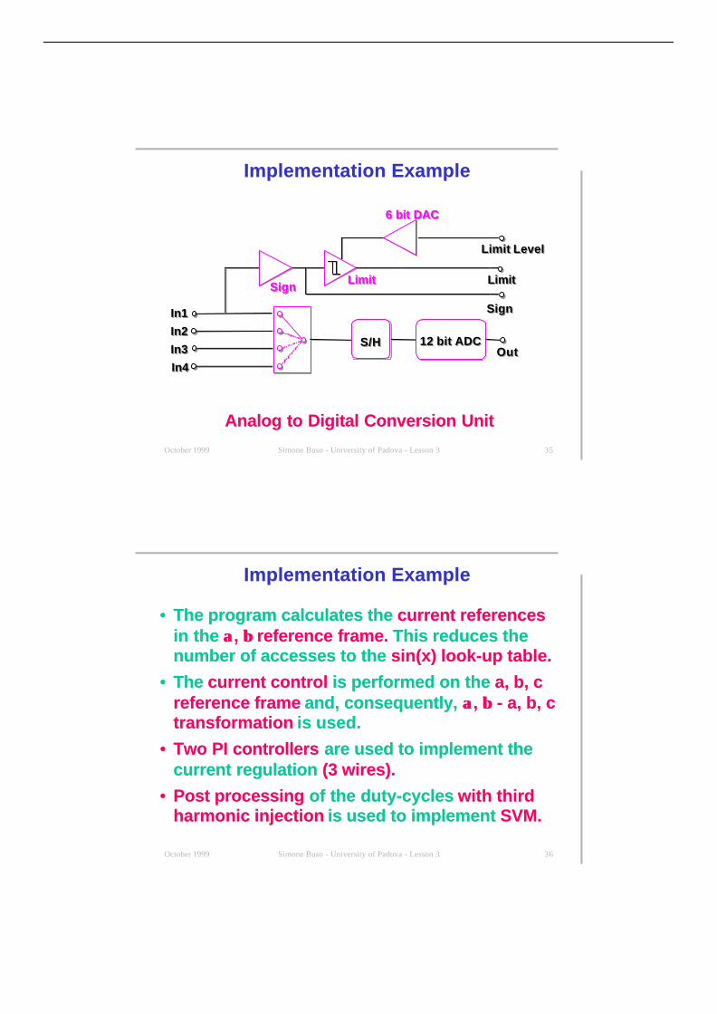
•• 3 12-bit 103 12-bit 10µµµµs A/Ds A/D converters each with 4 converters each with 4multiplexed inputsmultiplexed inputs
•• 77 comparators comparators to check input signals sign to check input signals sign•• 44 hysteresis comparators hysteresis comparators to check to check
overcurrentovercurrent condition condition•• 6-bit D/A converters6-bit D/A converters to set to set overcurrent overcurrent limit limit•• 4 additional sample & hold circuits4 additional sample & hold circuits
The analog ASIC includes:The analog ASIC includes:
Implementation ExampleImplementation Example
October 1999 35Simone Buso - University of Padova - Lesson 3
In1In1In1
In2In2In2
In3In3In3
In4In4In4
6 bit DAC6 bit DAC6 bit DAC
SignSignSign LimitLimitLimit
S/HS/HS/H 12 bit ADC12 bit ADC12 bit ADCOutOutOut
SignSignSign
LimitLimitLimit
Limit LevelLimit LevelLimit Level
Analog to Digital Conversion UnitAnalog to Digital Conversion Unit
Implementation ExampleImplementation Example
October 1999 36Simone Buso - University of Padova - Lesson 3
Implementation ExampleImplementation Example
•• The program calculates the The program calculates the current referencescurrent referencesin the in the αααα, , ββββ reference frame. reference frame. This reduces the This reduces thenumber of accesses to the number of accesses to the sin(x) look-up table.sin(x) look-up table.
•• The The current controlcurrent control is performed on the is performed on the a, b, ca, b, creference framereference frame and, consequently, and, consequently, αααα, , ββββ - a, b, c - a, b, ctransformationtransformation is used. is used.
•• Two PI controllersTwo PI controllers are used to implement the are used to implement thecurrent regulation current regulation (3 wires).(3 wires).
•• Post processingPost processing of the duty-cycles of the duty-cycles with thirdwith thirdharmonic injectionharmonic injection is used to implement is used to implement SVM.SVM.

October 1999 37Simone Buso - University of Padova - Lesson 3
; ; Alfa-Beta Current Reference GenerationAlfa-Beta Current Reference Generation;; MOVE MOVE X1,INCREMX1,INCREM ; Load increment; Load increment MOVE MOVE A1,THETA ; Load current result in the A1,THETA ; Load current result in the ; accumulator; accumulator ADD A1,X1 ADD A1,X1 ; Sum THETA + INCREM and; Sum THETA + INCREM and MOVE MOVE THETA,A1 ; move the result in THETATHETA,A1 ; move the result in THETA;;SINSIN MOVE MOVE X0,THETAX0,THETA ; Calculate sin; Calculate sin TAB SINTAB,7TAB SINTAB,7 ;; MOVE MOVE IA_REF,A1IA_REF,A1 ; Store it in IA_REF=Sin(THETA); Store it in IA_REF=Sin(THETA) MOVE MOVE A1,THETA A1,THETA ;; MOVE MOVE X1,HALF X1,HALF ; THETA + 90 degrees; THETA + 90 degrees ADD ADD A1,X1A1,X1 ;; MOVE X0,A1 MOVE X0,A1 ;; TAB SINTAB,7 TAB SINTAB,7 ;; MOVE IB_REF,A1 ; IB_REF=Sin(THETA+90) MOVE IB_REF,A1 ; IB_REF=Sin(THETA+90)
Implementation ExampleImplementation Example
October 1999 38Simone Buso - University of Padova - Lesson 3
Implementation ExampleImplementation Example; Alfa-Beta -> U,V,Z Transform; Alfa-Beta -> U,V,Z Transform;;TRSF23TRSF23 MOVE MOVE X1,TWO_THIRDSX1,TWO_THIRDS ; ; MOVE MOVE Y1,IA_REFY1,IA_REF ;; MUL MUL X1,Y1X1,Y1 X0,SIN_60X0,SIN_60 ;; MOVE MOVE IU_REF,A1IU_REF,A1 ; IU_REF = 2/3*IA_REF; IU_REF = 2/3*IA_REF MOVE MOVE Y0,IB_REFY0,IB_REF ;; MUL MUL X0,Y0X0,Y0 ;; MOVE MOVE X0,A1X0,A1 ;; MUL MUL X0,X1 X0,X1 Y0,SIN_30Y0,SIN_30 ;; MOVE MOVE X0,A1X0,A1 ;; MOVE MOVE Y1,IU_REFY1,IU_REF ;; MUL MUL Y0,Y1Y0,Y1 ;; ADDADD -A1,X0-A1,X0 ; ; MOVE MOVE IV_REF,A1IV_REF,A1 ; IV_REF = 1/SQRT(3)*IB_REF; IV_REF = 1/SQRT(3)*IB_REF
-1/3*IA_REF-1/3*IA_REF

October 1999 39Simone Buso - University of Padova - Lesson 3
PI_UPI_U ; PI phase U; PI phase U MOVE MOVE X1,IU_ANAX1,IU_ANA ;; MOVE MOVE A1,IU_RFA1,IU_RF ;; SUBL SUBL A1,X1A1,X1 ;; MOVE MOVE ERROR,A1ERROR,A1 ; Control input variable; Control input variable MOVE MOVE Y1,KPUY1,KPU ; Proportional gain; Proportional gain MOVE MOVE X1,A1X1,A1 ;; MUL MUL X1,Y1X1,Y1 X0,UCOMPX0,UCOMP ; Proportional part OK; Proportional part OK ADDL ADDL A1,X0A1,X0 X0,LIMPOSX0,LIMPOS ; Feed-forward compensation; Feed-forward compensation LIMSLIMS A1,X0A1,X0 Y0,LIMNEGY0,LIMNEG ;; LIMI LIMI A1,X0A1,X0 PROPU,A1PROPU,A1 ; Anti wind-up for the; Anti wind-up for the MOVE MOVE A,INTEGUA,INTEGU ; integral part; integral part MOVE MOVE Y1,KIUY1,KIU ;; MACLMACL X1,Y1X1,Y1 ;; LIM LIM X0,Y0 X0,Y0 X1,PROPUX1,PROPU ;; ADDL ADDL A1,X1 A1,X1 INTEGU,AINTEGU,A ; N.B. The ; N.B. The movemove is executed is executed ; before the ; before the addadd MOVE MOVE UREF,A1UREF,A1 ; end PI phase U; end PI phase U
Implementation ExampleImplementation Example
October 1999 40Simone Buso - University of Padova - Lesson 3
MODULAMODULA ; SVM part of the program; SVM part of the program MOVE MOVE Y0,UREFY0,UREF ;; MOVE MOVE Y1,VREFY1,VREF ;; HAR3 HAR3 MOVE MOVE Y1,A1Y1,A1 ;; MOVE MOVE THIRD,Y1THIRD,Y1 ;;;;; Switching instants; Switching instants;; MOVE MOVE X0,MODE_UX0,MODE_U ; Load PWM mode; Load PWM mode MOVE MOVE Y1,THIRDY1,THIRD ; Calculate ‘third harmonic’; Calculate ‘third harmonic’ MOVE MOVE Y0,TMOD_1Y0,TMOD_1 ; Limit to TMOD - 1 (PWM); Limit to TMOD - 1 (PWM) MOVE MOVE A1,UREFA1,UREF ; Load voltage reference; Load voltage reference MOVE MOVE X1,TMOD_2X1,TMOD_2 ;; ADD ADD A1,Y1A1,Y1 ; Load third harmonic; Load third harmonic PWMPWM A1,X1A1,X1 ; Calculate instant TU1; Calculate instant TU1 LIMULIMU A1,Y0A1,Y0 ; Limit TU1 to TMOD_1; Limit TU1 to TMOD_1 MOVE MOVE TU1,A1TU1,A1 ; Store the result; Store the result
Implementation ExampleImplementation Example

October 1999 41Simone Buso - University of Padova - Lesson 3
[1][1] L.L. Rossetto Rossetto, L., L. Malesani Malesani, P., P. Tenti Tenti, S., S. Buso Buso, A., A.PollmannPollmann: : "Fully Digital Control of a Three Phase UPS"Fully Digital Control of a Three Phase UPSbyby VeCon VeCon Integrated Controller" Integrated Controller" IEEE Industry IEEE IndustryApplications Society (IAS) Annual Meeting,Applications Society (IAS) Annual Meeting, Orlando Orlando,,October 8-12, 1995, pp. 2663-2669.October 8-12, 1995, pp. 2663-2669.
[2][2] E. Kiel and W.E. Kiel and W. Schumacher Schumacher, , ""VeConVeCon: A High-: A High-Performance Single-Chip-Performance Single-Chip-ServocontrollerServocontroller for AC for ACDrives",Drives", IPEC IPEC Conf Conf.. Proc Proc., 1995, pp. 1284-1289.., 1995, pp. 1284-1289.
ReferencesReferences