digital electronics (extended candidates)
TRANSCRIPT
Save My Exams! – The Home of RevisionFor more awesome GCSE and A level resources, visit us at www.savemyexams.co.uk/
Digital electronics (extended
candidates)
Question Paper 1
Level IGCSE
ExamBoard CIE
Topic Electricity and Magnetism
Sub-Topic Digital electronics (extended candidates)
Paper Type (Extended) Theory Paper
Booklet Question Paper 1
Time Allowed: 58 minutes
Score: /48
Percentage: /100
Subject Physics

1 (a) (i) Fig. 10.1 shows the symbol for a circuit component.
Fig. 10.1
Name this component.
................................................................................................................................ [1]
(ii) In the space below, draw the symbol for a NOT gate.
[1](b) Fig. 10.2 shows a digital circuit.
AB
D E
C
Fig. 10.2
Complete the truth table for this circuit.
output Einput Doutput Cinput Binput A
000
100
010
110
001
101
011
111
[3]
Save My Exams! – The Home of Revision For more awesome GCSE and A level resources, visit us at www.savemyexams.co.uk/

Suggest a modification to the circuit in Fig. 10.2 to produce the output Z in the truth table below.It may help you to compare this truth table with the truth table in (b).
(c)
output Zinput Dinput Binput A
0000
0100
0010
0110
0001
0101
0011
1111
...........................................................................................................................................
........................................................................................................................................... [1]
[Total: 6]
Save My Exams! – The Home of Revision For more awesome GCSE and A level resources, visit us at www.savemyexams.co.uk/

2 (a) (i) Fig. 11.1 shows the symbol for a logic gate and its truth table.
outputA
B
input A input B output0101
0011
0001
Fig. 11.1
State the name of this logic gate. ............................................................[1]
(ii) Complete the truth table for the logic gate shown in Fig. 11.2.
outputA
B
input A input B output0101
0011
Fig. 11.2[2]
(b) Fig. 11.3 shows the system of logic gates used to ensure the security of the strongroom of abank.
A
B
C
D
E
F
Fig. 11.3
The strongroom door will only open when the output F is logic 1.
Complete the table to show the logic states at A, B, C, D and E when the strongroom door can be opened.
input A input B input C output D output E output F
1
[3]
[Total: 6]
Save My Exams! – The Home of Revision For more awesome GCSE and A level resources, visit us at www.savemyexams.co.uk/

3 Fig. 8.1 is a schematic diagram of an electronic circuit controlling a lamp.
temperaturesensor
lightsensor
relay lamp
AB
Fig. 8.1
The output of the temperature sensor is high (logic 1) when it detects raised temperatures. The output of the light sensor is high (logic 1) when it detects raised light levels.
The lamp is lit when the input to the relay is high (logic 1).
(a) Complete the truth table by giving the outputs of A and B.
[2]
(b) State the conditions under which the lamp is lit.
[1]
(c) Suggest why B is connected to a relay, rather than directly to the lamp.
[2]
[Total: 5]
Save My Exams! – The Home of Revision For more awesome GCSE and A level resources, visit us at www.savemyexams.co.uk/

4 (a) Fig. 10.1 shows the symbol for a logic gate.
Fig. 10.1
(i) State the name of this gate. ......................................... [1]
[1] (ii) On Fig. 10.1, label an input and an output.
(iii) In the space below, draw the symbol for a NAND gate.
[1]
Save My Exams! – The Home of Revision For more awesome GCSE and A level resources, visit us at www.savemyexams.co.uk/

(b) A very low frequency alternating voltage is applied between A and B in the circuit shown inFig. 10.2.
A
centre-zeroammeter
A B
Fig. 10.2
On each diagram, draw a possible position of the indicator needle of the ammeter at the time in the cycle when
(i) A is positive and B is negative,
–1 0 +1–2 +2
A
(ii) there is no p.d. between A and B,
–1 0 +1–2 +2
A
(iii) A is negative and B is positive.
–1 0 +1–2 +2
A
[3]
[Total: 6]
Save My Exams! – The Home of Revision For more awesome GCSE and A level resources, visit us at www.savemyexams.co.uk/

5 (a) Fig. 9.1 shows the symbol for a logic gate.
Fig. 9.1
(i) State the name of this gate.
...........................................................................................................................................
(ii) On Fig. 9.1, clearly label an input and an output.[2]
(b) In the space below, draw the symbol for a fuse.
[1]
(c) Fig. 9.2 shows a circuit.
A
B
6 V
Fig. 9.2
Component A is not emitting light. It only emits light when the p.d. across it is greater than 1 V.
(i) A change to the environment around component B causes component A to emit light.
State the environmental change.
.......................................................................................................................................[1]
Save My Exams! – The Home of Revision For more awesome GCSE and A level resources, visit us at www.savemyexams.co.uk/

(ii) Explain your answer to (i).
...........................................................................................................................................
...........................................................................................................................................
...........................................................................................................................................
.......................................................................................................................................[3]
(d) The combined resistance of the two resistors shown in Fig. 9.3 is 4.0 Ω.
R
6.0
Fig. 9.3
Calculate the resistance of resistor R.
resistance of R = ...........................................................[2]
[Total: 9]
Save My Exams! – The Home of Revision For more awesome GCSE and A level resources, visit us at www.savemyexams.co.uk/

6 (a) Fig. 10.1 shows a digital logic circuit, not using the recognised symbols.
AND gate
OR gate
D
output E
input A
input B
input C
Fig. 10.1
Complete the table below to indicate the logic levels of points D and E in the circuit, when points A, B and C are at the logic levels indicated.0 represents low or off. 1 represents high or on.
A B C D E
00 0
00 0
11 1
[3]
(b) Draw the recognised symbol for an AND gate.
[1]
(c) A NAND gate can be replaced by an AND gate and a NOT gate.
Draw a diagram to show how the AND gate and the NOT gate should be connected. Labelclearly the logic gates and any input or output.
[2]
[Total: 6]
Save My Exams! – The Home of Revision For more awesome GCSE and A level resources, visit us at www.savemyexams.co.uk/

7 Fig. 10.1 is the symbol for a NAND gate with inputs A and B.
input A
input Boutput
Fig. 10.1
(a) Input A and input B can be set to 1 (high) or to 0 (low).
Complete the table below to give the outputs for this NAND gate.
input A
inputB
output
00
10
1 0
1 1
[1]
(b) The two inputs of the NAND gate are joined together and connected to an input C, asshown in Fig. 10.2.
input C output
Fig. 10.2
(i) Determine the output of this NAND gate when
1. input C is set to 0,
output = .......................................................
2. input C is set to 1.
output = .......................................................[1]
Save My Exams! – The Home of Revision For more awesome GCSE and A level resources, visit us at www.savemyexams.co.uk/

(ii) State the name of the logic gate that behaves in the same way as the NAND gate inFig. 10.2.
............................................................................................................................. [1]
(c) A circuit combines three NAND gates.
The inputs to the circuit are P and Q, as shown in Fig. 10.3.
P
Q
TR
S
Fig. 10.3
Points R, S and T in the circuit are also labelled.
Input P is set to 0 and input Q is set to 1.
Determine the logic states (0 or 1) of points R, S and T.
point R = ..............................
point S = ..............................
point T = ..............................[2]
[Total: 5]
Save My Exams! – The Home of Revision For more awesome GCSE and A level resources, visit us at www.savemyexams.co.uk/
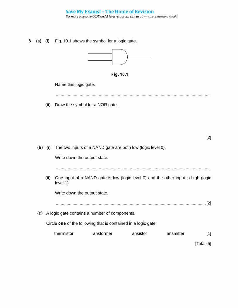
8 (a) (i) Fig. 10.1 shows the symbol for a logic gate.
Fig. 10.1
Name this logic gate.
..................................................................................................................................
(ii) Draw the symbol for a NOR gate.
[2]
(b) (i) The two inputs of a NAND gate are both low (logic level 0).
Write down the output state.
..................................................................................................................................
(ii) One input of a NAND gate is low (logic level 0) and the other input is high (logiclevel 1).
Write down the output state.
.............................................................................................................................. [2]
(c) A logic gate contains a number of components.
Circle one of the following that is contained in a logic gate.
thermistoror ansformer ansistorst ansmitter [1]
[Total: 5]
Save My Exams! – The Home of Revision For more awesome GCSE and A level resources, visit us at www.savemyexams.co.uk/