digital electronics it0203 semester 3 4.pdf · digital electronics & it0203 semester ‐3 ......
TRANSCRIPT

DIGITAL ELECTRONICS & it0203Semester ‐ 3
P.Rajasekar & C.M.T.KarthigeyanAsst.Professor
SRM University, Kattankulathur
1

Disclaimer
The contents of the slides are solely for the purpose of teaching students at SRM University. All copyrights and Trademarks of organizations/persons apply even if not specified explicitly.
2

UNIT 4 ‐ SEQUENTIAL CIRCUIT
3

Overview
• Synchronous Sequential Logic– Introduction to sequential circuits
– Types of sequential circuits
– Storage elements• Latches
• Flip‐flops
– Sequential circuit analysis• State tables
• Design Procedure
4

Introduction to Sequential Circuits
• A Sequential circuit contains:– Storage elements:
Latches or Flip‐Flops – Combinational Logic:
• Implements a multiple‐output switching function
• Inputs are signals from the outside.• Outputs are signals to the outside.• Other inputs, State or Present State, are signals from storage elements.
• The remaining outputs, Next State are inputs to storage elements.
Combina‐tionalLogicStorage
Elements
Inputs Outputs
StateNextState
5

• Combinatorial Logic– Next state function
Next State = f(Inputs, State)– Output function (Mealy)
Outputs = g(Inputs, State)– Output function (Moore)
Outputs = h(State)• Output function type depends on specification and affects the
design significantly
Combina‐tionalLogicStorage
Elements
Inputs Outputs
StateNextState
Introduction to Sequential Circuits
6

7
Types of Sequential Circuits
• Depends on the times at which:– storage elements observe their inputs, and – storage elements change their state
• Synchronous– Behavior defined from knowledge of its signals at discrete
instances of time– Storage elements observe inputs and can change state only
in relation to a timing signal (clock pulses from a clock)
• Asynchronous– Behavior defined from knowledge of inputs an any instant of
time and the order in continuous time in which inputs change
– If clock just regarded as another input, all circuits are asynchronous!
– Nevertheless, the synchronous abstraction makes complex designs tractable!

Basic (NAND) S – R Latch
• “Cross‐Coupling” two NAND gates gives the S ‐RLatch:
• Which has the time sequence behavior:
• S = 0, R = 0 is forbidden as input pattern
QS (set)
R (reset) Q
R S Q Q Comment1 1 ? ? Stored state unknown1 0 1 0 “Set” Q to 11 1 1 0 Now Q “remembers” 10 1 0 1 “Reset” Q to 01 1 0 1 Now Q “remembers” 00 0 1 1 Both go high1 1 ? ? Unstable!
Time
8

Basic (NOR) S – R Latch
• Cross‐coupling twoNOR gates gives theS – R Latch:
• Which has the time sequence behavior:
S (set)
R (reset)Q
Q
R S Q Q Comment0 0 ? ? Stored state unknown0 1 1 0 “Set” Q to 10 0 1 0 Now Q “remembers” 11 0 0 1 “Reset” Q to 00 0 0 1 Now Q “remembers” 01 1 0 0 Both go low0 0 ? ? Unstable!
Time
9

Clocked S ‐ R Latch
• Adding two NANDgates to the basicS ‐ R NAND latchgives the clockedS – R latch:
• Has a time sequence behavior similar to the basic S‐R latch except that the S and R inputs are only observed when the line C is high.
• C means “control” or “clock”.
S
R
Q
C
Q
10
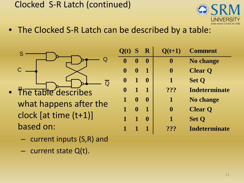
Clocked S‐R Latch (continued)
• The Clocked S‐R Latch can be described by a table:
• The table describeswhat happens after theclock [at time (t+1)]based on:– current inputs (S,R) and
– current state Q(t).
Q(t) S R Q(t+1) Comment0 0 0 0 No change0 0 1 0 Clear Q0 1 0 1 Set Q0 1 1 ??? Indeterminate1 0 0 1 No change1 0 1 0 Clear Q1 1 0 1 Set Q1 1 1 ??? Indeterminate
S
R
Q
Q
C
11

D Latch
• Adding an inverterto the S‐R Latch,gives the D Latch:
• Note that there areno “indeterminate”states!
Q D Q(t+1) Comment
0 0 0 No change0 1 1 Set Q1 0 0 Clear Q1 1 1 No Change
The graphic symbol for aD Latch is:
C
D Q
Q
DQ
C
Q
12

Flip‐Flops
• The latch timing problem
• Master‐slave flip‐flop
• Edge‐triggered flip‐flop
• Standard symbols for storage elements
• Direct inputs to flip‐flops
13
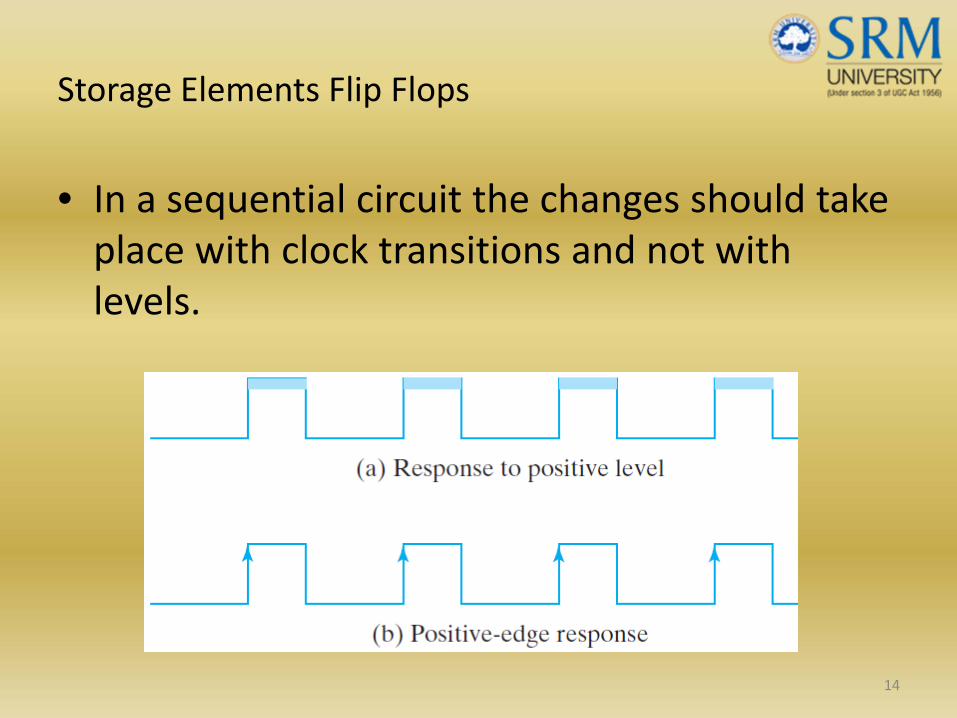
Storage Elements Flip Flops
• In a sequential circuit the changes should take place with clock transitions and not with levels.
14

• Consists of two clockedS‐R latches in serieswith the clock on the second latch inverted
• The input is observedby the first latch with C = 1
• The output is changed by the second latch with C = 0 • The path from input to output is broken by the difference
in clocking values (C = 1 and C = 0).• The behavior demonstrated by the example with D driven
by Y given previously is prevented since the clock must change from 1 to 0 before a change in Y based on D can occur.
C
S
R
Q
Q
CR
Q
Q
C
S
R
QS
Q
S‐R Master‐Slave Flip‐Flop
15

Flip‐Flop Solution
• Use edge‐triggering instead of master‐slave
• An edge‐triggered flip‐flop ignores the pulse while it is at a constant level and triggers only during a transition of the clock signal
• Edge‐triggered flip‐flops can be built directly at the electronic circuit level, or
• A master‐slave D flip‐flop which also exhibits edge‐triggered behavior can be used.
16

Edge‐Triggered D Flip‐Flop
• The edge‐triggered D flip‐flop is thesame as the master‐slave D flip‐flop
• It can be formed by:– Replacing the first clocked S‐R latch with a clocked D latch or
– Adding a D input and inverter to a master‐slave S‐R flip‐flop
• The change of the D flip‐flop output is associated with the negative edge at the end of the pulse
• It is called a negative‐edge triggered flip‐flop
C
S
R
Q
QC
Q
QC
D QD
Q
17
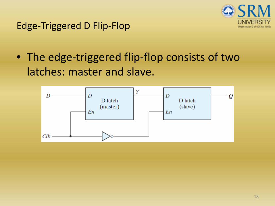
Edge‐Triggered D Flip‐Flop
• The edge‐triggered flip‐flop consists of two latches: master and slave.
18

JK Flip‐Flop
• Other types of flip‐flops may be constructed from D flip‐flop. Two other types less commonly used are JK and T flip flops.
19

T Flip‐Flop
20

Flip Flop Characteristic Table
21

Flip Flop Characteristic Equations
22

Sequential Circuit Analysis
• General Model– Current Stateat time (t) is stored in an array offlip‐flops.
– Next State at time (t+1) is a Boolean function of State and Inputs.
– Outputs at time (t) are a Boolean function of State(t) &(sometimes)Inputs (t).
Combina‐tionalLogic
Inputs
StateNextState
Outputs
Storage Elements
CLK
23

Example
• Input: x(t)
• Output: y(t)
• State: ((A(t), B(t))
• What is the Output Function?
• What is the Next State Function?
AC
D Q
Q
C
D Q
Q
y
x A
B
CP
24

State Table Characteristics
• State table – a multiple variable table with the following four sections:– Present State – the values of the state variables for each allowed state.
– Input – the input combinations allowed.– Next‐state – the value of the state at time (t+1) based on the present state and the input.
– Output – the value of the output as a function of the present state and (sometimes) the input.
• From the viewpoint of a truth table:– the inputs are Input, Present State– and the outputs are Output, Next State
25

Example: State Table
• The state table can be filled in using the next state and output equations: A(t+1) = A(t)x(t) + B(t)x(t) B(t+1) =⎯A (t)x(t) y(t) =⎯x (t)(B(t) + A(t))
Present State Input Next State OutputA(t) B(t) x(t) A(t+1) B(t+1) y(t)0 0 0 0 0 00 0 1 0 1 00 1 0 0 0 10 1 1 1 1 01 0 0 0 0 11 0 1 1 0 01 1 0 0 0 11 1 1 1 0 0
26

Example: Alternate State Table
• 2‐dimensional table that matches well to a K‐map. Present state rows and input columns in Gray code order. – A(t+1) = A(t)x(t) + B(t)x(t)
– B(t+1) =⎯A (t)x(t)– y(t) =⎯x (t)(B(t) + A(t))
Present State
Next Statex(t)=0 x(t)=1
Outputx(t)=0 x(t)=1
A(t) B(t) A(t+1)B(t+1) A(t+1)B(t+1) y(t) y(t)0 0 0 0 0 1 0 00 1 0 0 1 1 1 01 0 0 0 1 0 1 01 1 0 0 1 0 1 0
27

State Diagram
28

Analysis with JK Flip Flops
• Determine flip‐flop input equations in terms of present state and inputs.
• For each JKFF determine J=f(Q(t),x(t)) and K=g(Q(t),x(t))
• Using the flip‐flop characteristic table determine the next state values in the state table.
• Substitute equations for J and K into Q(t+1)=JQ’+K’Q to calculate the values of next‐states
29

Analysis with JK FF
30

State Table
31

State Diagram
32

Excitation Tables
• Input equations for D‐FF is obtained directly from next state
• For JK and T FFs FF input equations cannot be obtained easily from state table.
• A table that lists the inputs for a given change of state is needed.
• It is called excitation table
33

Excitation Tables
34
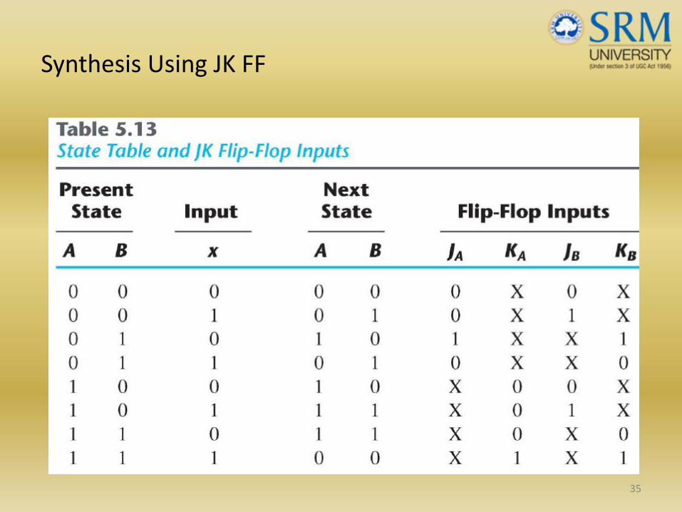
Synthesis Using JK FF
35

Synthesis Using JK FF
36

Synthesis Using JK FF
37

Shift Register
• A register capable of shifting the binary information held in each cell to its neighboring cell, is called a shift register.
• Serial input is shifted to right with each clock pulse.After four clock pulses serial input appears
• at the Serial output.
38

Serial Transfer
• A digital system operates at serial mode: information transferred and manipulated one bit at a time.
• Serial transfers take place with the system clock.
• In the next clock contents of shift register A is transferred to shift register B.
39

Serial Transfer
40
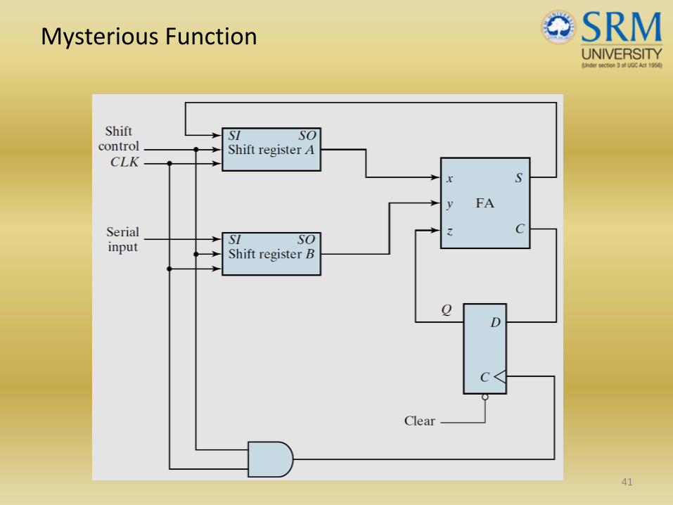
Mysterious Function
41

Serial Adder• Two binary numbers to be added are stored in two shift registers A and B.
• The shift registers are shifted right starting with least significant bit, the bits are added by the full adder and carry is stored in a D flip‐flop.
• When the addition is completed the sum is in regiater A.
• Serial adder will require n clock pulses for adding n‐bit numbers. A parallel adder can perform the n‐bit addition in one clock pulse period.
• However a parallel adder will have n full adders.
42
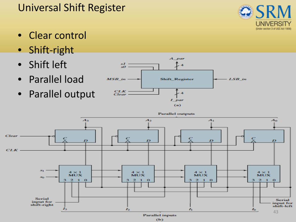
Universal Shift Register
• Clear control • Shift‐right • Shift left • Parallel load • Parallel output
43

Counters
• A register that goes through a prescribed sequence of states upon application of input pulses is called a counter.
• A counter that follows binary number sequence is called a binary counter
• n‐bit binary counter consists of n flip‐flops and count from 0 to 2^n‐1.
44
Ripple Counters
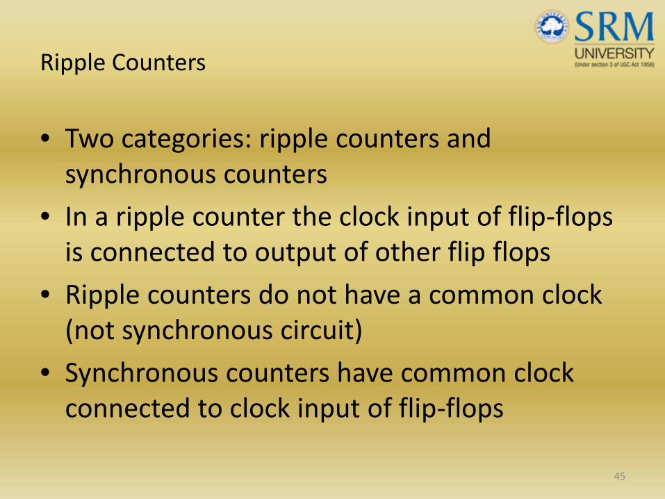
• Two categories: ripple counters and synchronous counters
• In a ripple counter the clock input of flip‐flops is connected to output of other flip flops
• Ripple counters do not have a common clock (not synchronous circuit)
• Synchronous counters have common clock connected to clock input of flip‐flops
45

Ripple Counters
Chapter 6 ‐ Fall 10 46

Up‐Down Counter
47

BCD Counter
48

BCD Counter
49

Ring Counter
50

Johnson Counter
Chapter 6 ‐ Fall 10 51

Counters With Unused States
52
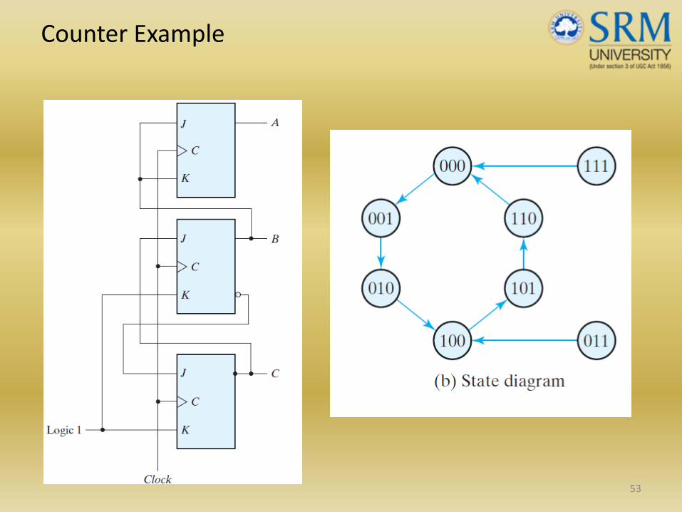
Counter Example
53

bibliography
• Charles H. Roth‐ Jr., Fundamentals of logic design, Thomson Asia,5th edition‐2004 (CH1,CH2,CH3,CH4,CH5,CH6,CH7,CH9,CH11,CH12)
• M. Morris Mano, Digital Logic and Computer Design, Prentice Hall of India
• Floyd, Digital Fundamentals, Universal Book Stall, 3rd Edition,1986
• Morris Mano, Digital Design, Prentice Hall of India, 2nd Edition 1991
• Bigell & Donovan, Digital Electronics, Thomson Asia Pvt. Ltd., 4th Edition
54

Review questions
1. State the difference between combinational circuits and sequential circuits?
2. What do you mean by Latches?3. Give the difference between latches and
flip flops?4. Define Flipflops?5. List the design procedures for designing a
sequential circuit?6. State the operation of S‐R flipflop?7. State the operation of T‐fliflop?8. State the features of clocked T flipflop?
55

Review questions
9. Give the characteristics equation for S‐R , T,J‐K and D‐flipflop?
10.What is a counter?11.What is a buffer register?12.List the types of shift register?13.How do you convert JR flipflop into D
flipflop?14.How do you convert T flipflop into D‐
flipflop?15.Give the counter applications?
56