digital hardware design laboratory mini-projectneeraj/ta/cs316/2005-2006/project/final/... ·...
TRANSCRIPT

DIGITAL HARDWARE DESIGN LABORATORY MINI-PROJECT
LOGIC ANALYSER
By:-
Pulkit Gambhir (2003cs10181) Aditya Dev Nayar (2003cs50207) CYCLE 1
Instructor: Prof M. Balakrishnan Teaching Assistant: Anant Vishnoi
INDEX:
(click on any of the following links) (1) Title page (above) (2) Specifications(3) Design Description (4) Simulation (5) Implementation Results(6) Conclusions
ANNEXURE
(i) VHDL code(ii) C++ code(iii) Matlab code
List of tools used:
a) Xilinx foundation 4 for the whole circuit design b) Altera maxplus 2 baseline for VHDL simulation c) INCODE to download/upload data from FPGA d) GNU c++ compiler to convert txt files to readable format e) Matlab to display a snapshot of captured history

The bigger picture:
RAM writing logic
Micro- controller & PC interfacing
GUI display on the PC
Capture now signal
Data ready controls
4 input channels
Keyboard
Registers to store trigger pattern
Registers to capture actual data from
channels
4 input channels
Comparison logic
P L A
Special decoding logic for OR (**) cases
Capture now signal
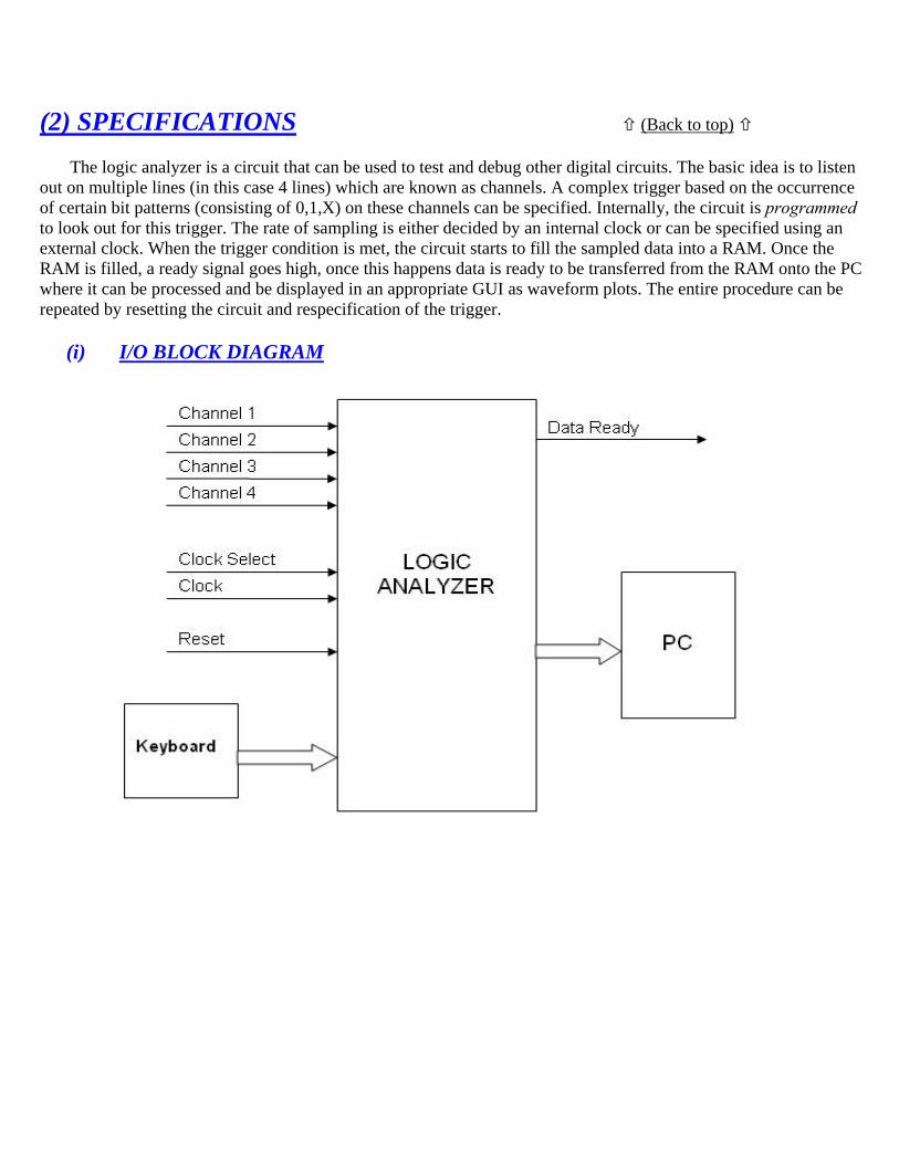
(2) SPECIFICATIONS (Back to top)
The logic analyzer is a circuit that can be used to test and debug other digital circuits. The basic idea is to listen out on multiple lines (in this case 4 lines) which are known as channels. A complex trigger based on the occurrence of certain bit patterns (consisting of 0,1,X) on these channels can be specified. Internally, the circuit is programmed to look out for this trigger. The rate of sampling is either decided by an internal clock or can be specified using an external clock. When the trigger condition is met, the circuit starts to fill the sampled data into a RAM. Once the RAM is filled, a ready signal goes high, once this happens data is ready to be transferred from the RAM onto the PC where it can be processed and be displayed in an appropriate GUI as waveform plots. The entire procedure can be repeated by resetting the circuit and respecification of the trigger.
(i) I/O BLOCK DIAGRAM

(ii) User Interface (Back to top)
Input Interface
(a) Master reset: In the beginning the circuit must be reset to bring all state machines into their initial states, and to clear all registers of any junk data if any, then set it back to low.
(b) Clock select / EXT clock / INT clock :
Clock select = high To sample your input at the internal clock of 490 Hz
Clock select = low To sample your input with an optionally provided external clock
(c) Specifying the trigger condition to start capture
User input is needed to specify the trigger condition. This is done using a keyboard whose key-maps are explained below.
0
Logic 0
1
Logic 1
X
Don’t Care
CH1
Channel 1 select
CH2
Channel 2 select
CH3
Channel 3 select
CH4
Channel 4 select
, comma, sequence
delimiter
** Double star, OR
operator
* Star, start symbol for
circuit
@
At-Rate, AND operartor
#
Hash, end symbol
Symbol/Key Meanings
* : Start Symbol # : End Symbol
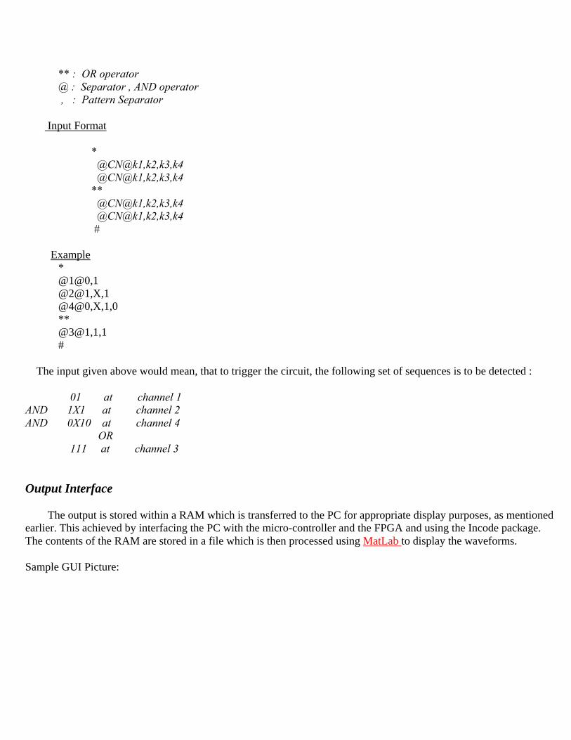
** : OR operator @ : Separator , AND operator , : Pattern Separator
Input Format
* @CN@k1,k2,k3,k4 @CN@k1,k2,k3,k4 ** @CN@k1,k2,k3,k4 @CN@k1,k2,k3,k4 #
Example
* @1@0,1 @2@1,X,1 @4@0,X,1,0 ** @3@1,1,1 #
The input given above would mean, that to trigger the circuit, the following set of sequences is to be detected :
01 at channel 1 AND 1X1 at channel 2 AND 0X10 at channel 4 OR 111 at channel 3
Output Interface
The output is stored within a RAM which is transferred to the PC for appropriate display purposes, as mentioned earlier. This achieved by interfacing the PC with the micro-controller and the FPGA and using the Incode package. The contents of the RAM are stored in a file which is then processed using MatLab to display the waveforms.
Sample GUI Picture:
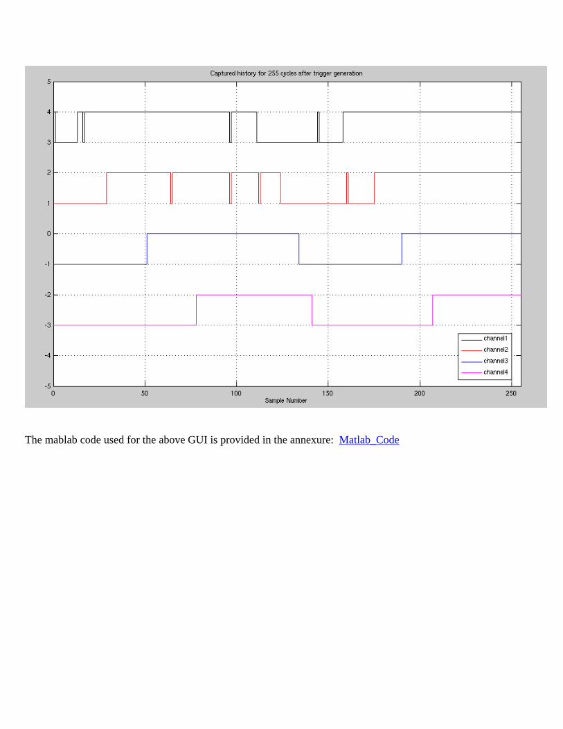
The mablab code used for the above GUI is provided in the annexure: Matlab_Code

(3) Design Description (Back to top)
Design Modules: The whole circuit can be described by the following 9 modules (data part and control part shown separately)
(i) Trigger Programming & Capturing Portion
Data Part:
1. Keyboard interfacing module 2. Register for trigger pattern storage 3. Circuit to check pattern match 4. mini-PLA to generate trigger output
Control Part:
5.Input state machine
(ii) RAM Writing, storing the state of the circuit after trigger generation
Data Part:
6. 256 X 8 Synchronous RAM
Control Part:
7. State machine to write into RAM sequentially
(iii) Communication Portion, PC interfacing to upload data to a file, through INCODE
8. Micro-controller interfacing with RAM to transfer data to PC 9. Matlab generated waveforms of captured data.
(I) Trigger Programming & Capturing Portion
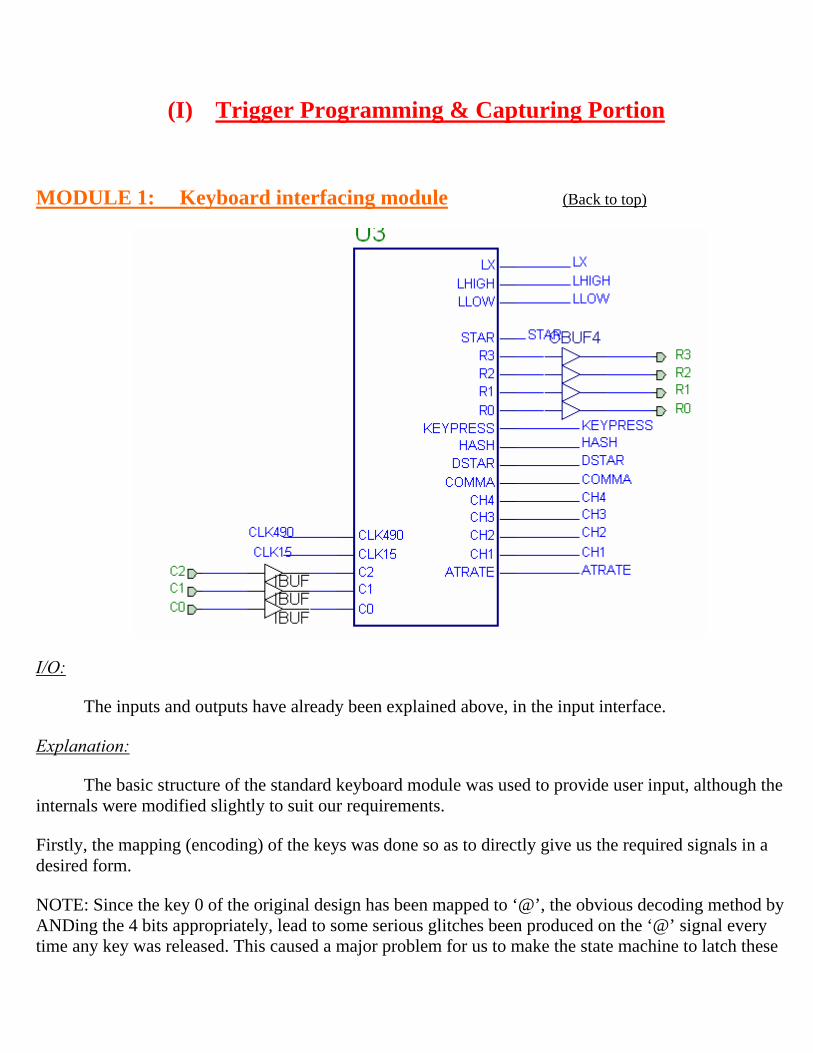
MODULE 1: Keyboard interfacing module (Back to top)
I/O:
The inputs and outputs have already been explained above, in the input interface.
Explanation:
The basic structure of the standard keyboard module was used to provide user input, although the internals were modified slightly to suit our requirements.
Firstly, the mapping (encoding) of the keys was done so as to directly give us the required signals in a desired form.
NOTE: Since the key 0 of the original design has been mapped to ‘@’, the obvious decoding method by ANDing the 4 bits appropriately, lead to some serious glitches been produced on the ‘@’ signal every time any key was released. This caused a major problem for us to make the state machine to latch these

outputs. This problem was corrected by introducing FLIP-FLOP’s in the original ‘K-BORD’ module which delayed the output bits by one cycle. The constraints and the UCF files for this modulehave been provided at the end of the report.
MODULE 2: Register for trigger pattern storage (Back to top)
There are 4 such registers, one for each channel.
I/O:
Inputs: 0,1,X goes high if data from Keyboard is logic zero, one or
don’t care respectively
LDBIT_CLK goes high if current channel’s data is to be latched.
INCBIT_CLK goes high if current channel’s next bit is about to come
ie, when the user has pressed comma on the current channel
CLR_REG when the full circuit is reset, this clears the data already stored
CLR_CNT when the full circuit is reset, this clears the counter keeping
Account of how many data bit have been input
Outputs: REG_OUT[7:0] The final output of the circuit is a sequence of encoded 8 bits

finally encoded and ready for equality check. The encoding
has been described below
Storing the trigger pattern Working and explanation
The trigger pattern can consist of a series of 0 , 1 and X. This circuit supports patterns of maximum length 4. In case a pattern of more than 4 characters is entered by the user, the last 4 bits of that pattern are used. Any pattern of less than 4 bits is padded with X's as far as internal implementation is concerned. On the same lines, if no pattern is specified for a particular channel, the pattern is taken to be XXXX. The pattern is encoded as per the following key :
10 → 0 11 → 1 00 → X The particular choice of coding has been made because by setting 00 to don't care; the patterns are all automatically reset to XXXX, whenever the entire circuit is reset and all registers cleared.

The logic at the top converts the 0 , 1 , X signals from the keyboard to the encoded form mentioned above. A 2-bit counter is run from 0 through till 3 along with a decoder in order to decide which (encoded) bit is being written in the register. Note that since each symbol is encoded into 2 bits and a maximum of 4 bit pattern may be entered, a register of length 8 has been used. The multiplexers ensure that when no bit is being written, the old value of the register is continually recycled back into it. The final output of the module is the current contents of the register.
MODULE 3: Checking Pattern Match (Back to top)
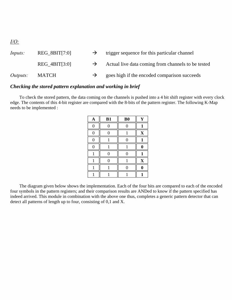
I/O:
Inputs: REG_8BIT[7:0] trigger sequence for this particular channel
REG_4BIT[3:0] Actual live data coming from channels to be tested
Outputs: MATCH goes high if the encoded comparison succeeds
Checking the stored pattern explanation and working in brief
To check the stored pattern, the data coming on the channels is pushed into a 4 bit shift register with every clock edge. The contents of this 4-bit register are compared with the 8-bits of the pattern register. The following K-Map needs to be implemented :
A B1 B0 Y 0 0 0 1 0 0 1 X 0 1 0 1 0 1 1 0 1 0 0 1 1 0 1 X 1 1 0 0 1 1 1 1
The diagram given below shows the implementation. Each of the four bits are compared to each of the encoded four symbols in the pattern registers; and their comparison results are ANDed to know if the pattern specified has indeed arrived. This module in combination with the above one thus, completes a generic pattern detector that can detect all patterns of length up to four, consisting of 0,1 and X.


MODULE 4: PLA for trigger generation (Back to top)
PLA
4 4 4 4
Decoded outputs for sequential latching of trigger, for all 4 channels
4 Sequence select
4 Comparator outputs, high if match occurs
Trigger generated
Explanation: Once the input has been decoded and the registers programmed to look out for specific patterns; the problem is to make the particular AND-OR specification out of the 4 outputs from the first part. For this a mini-PLA has been implemented, which is 'programmed' as per the needs of the trigger.
The mini-PLA can be programmed to implement any 4 variable function (as is required in the current context). The inputs to the mini-PLA are through latched decoders so that as each term of the function to be implemented is selected, the last selected term is not 'forgotten'.
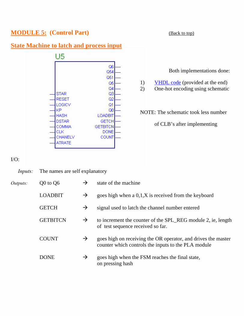
MODULE 5: (Control Part) (Back to top)
State Machine to latch and process input
Both implementations done:
1) VHDL code (provided at the end) 2) One-hot encoding using schematic
NOTE: The schematic took less number
of CLB’s after implementing
I/O:
Inputs: The names are self explanatory
Outputs: Q0 to Q6 state of the machine LOADBIT goes high when a 0,1,X is received from the keyboard GETCH signal used to latch the channel number entered GETBITCN to increment the counter of the SPL_REG module 2, ie, length of test sequence received so far. COUNT goes high on receiving the OR operator, and drives the master counter which controls the inputs to the PLA module DONE goes high when the FSM reaches the final state, on pressing hash

0
1
2
3
4
5
6
@
@
*
CN / getch
loadbit
logicV /
54
51
not*
not @
not CN
not @
not logicV /
X /
comma /
#
X
** /
logicV /
X /
RESET
not(getch) not(getbitcn) not(loadbit)
getbitcn
not(loadbit) getbitcn
done
count loadbit
count
(II) RAM Writing, storing the state of the circuit after trigger generation
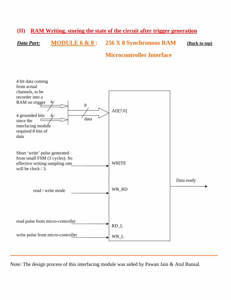
Data Part: MODULE 6 & 8 : 256 X 8 Synchronous RAM (Back to top)
Microcontroller Interface
Note: The design process of this interfacing module was aided by Pawan Jain & Atul Bansal.
AD[7:0] WRITE WR_RD RD_L WR_L
4
4
8
4 bit data coming from actual channels, to be recorder into a RAM on trigger
4 grounded bits since the interfacing module required 8 bits of data
data
Short ‘write’ pulse generated from small FSM (3 cycles). So effective writing sampling rate will be clock / 3.
read / write mode
Data ready
read pulse from micro-controller
write pulse from micro-controller

MODULE 7: State machine to write into RAM sequentially (Back to top)
Control Part:
The module is implemented using a generic state machine realization that increments a counter (whose output is used as write address ) and successfully generates read/write signals for the RAM. As a result the circuit when in write-mode can sample the inputs ( 4 channels ) at a rate proportional to the clock provided (divided by number of states in the machine) and store it in the RAM

0
1 / CE
2 / RW
(IV) Communication Portion, PC interfacing to upload data to a file, through INCODE
MODULE 9: Matlab generated waveforms of captured history. (Back to top)
3 4
RESET
X
X
X not(TC)
TC

RAM with written
data
INCODE kit TXT
file
GNU C++ compiler
ch1.txt ch2.txt ch3.txt ch4.txt
MATLAB
Snapshot results
1) From the uploaded file from INCODE, we generated txt file using the g++ GNU compiler in matlab readable format for each of the 4 channels.
ch1.txt g++ Code (provided in the annexure)
ch2.txt
ch3.txt
ch4.txt
2) Run matlab, and observe output. Matlab Code (provided in the annexure)

(4) SIMULATION (Back to top)
simulation state showing MATCH-B and CAPTURE-NOW


(5) IMPLEMENTATION RESULTS: (Back to top)
(i) UCF constraint file specs:
######################################### # CN 14 INPUTS from CN 10 or CN 11 # ######################################### NET CH1_SLI LOC=P39; NET CH2_SLI LOC=P40; NET CH3_SLI LOC=P44; NET CH4_SLI LOC=P45; NET FULL_RESET LOC=P35; NET CLK_SEL LOC=P36; NET EXT_CLK LOC=P37; #################################### # CN 17 for Key Board Inputs # #################################### NET R0 LOC=P56; NET R1 LOC=P57; NET R2 LOC=P58; NET R3 LOC=P59; NET C0 LOC=P60; NET C1 LOC=P61; NET C2 LOC=P62; #################################### # CN 13 OUTPUTS to CN 1 # #################################### NET VHDL_CSP0 LOC=P14; NET VHDL_CSP1 LOC=P15; NET VHDL_CSP2 LOC=P16; NET VHDL_CSP3 LOC=P17; NET VHDL_CSP4 LOC=P18; NET VHDL_CSP5 LOC=P19; NET VHDL_CSP6 LOC=P20; NET WRITE_READ LOC=P23; NET RESET_WRITE LOC=P24; NET TC_L_O LOC=P25; NET CAPTURE_NOW LOC=P26;

#################################### # Micro-controller connections # #################################### NET AD<0> LOC=P9; NET AD<1> LOC=P8; NET AD<2> LOC=P7; NET AD<3> LOC=P6; NET AD<4> LOC=P5; NET AD<5> LOC=P4; NET AD<6> LOC=P3; NET AD<7> LOC=P84; NET RD_L LOC=P83; NET WR_L LOC=P82;
(ii) Implementation Log Files (reports)
Design Summary: Number of errors: 0 Number of warnings: 2 Number of CLBs: 205 out of 400 51% CLB Flip Flops: 139 4 input LUTs: 251 (2 used as route-throughs) 3 input LUTs: 39 (10 used as route-throughs) 32X1 RAMs: 64 Number of bonded IOBs: 35 out of 61 57% IOB Flops: 0 IOB Latches: 0 Number of TBUFs: 89 out of 880 10% Number of OSC: 1 out of 1 100% Total equivalent gate count for design: 11120 Additional JTAG gate count for IOBs: 1680 Removed Logic Summary: 81 block(s) removed 97 block(s) optimized away 81 signal(s) removed Device utilization summary: Number of External IOBs 35 out of 160 57% Flops: 0
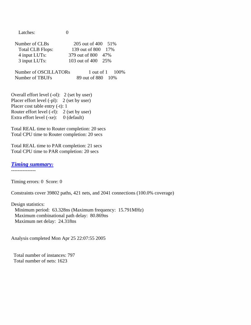
Latches: 0 Number of CLBs 205 out of 400 51% Total CLB Flops: 139 out of 800 17% 4 input LUTs: 379 out of 800 47% 3 input LUTs: 103 out of 400 25% Number of OSCILLATORs 1 out of 1 100% Number of TBUFs 89 out of 880 10% Overall effort level (-ol): 2 (set by user) Placer effort level (-pl): 2 (set by user) Placer cost table entry (-t): 1 Router effort level (-rl): 2 (set by user) Extra effort level (-xe): 0 (default) Total REAL time to Router completion: 20 secs Total CPU time to Router completion: 20 secs Total REAL time to PAR completion: 21 secs Total CPU time to PAR completion: 20 secs Timing summary: --------------- Timing errors: 0 Score: 0 Constraints cover 39802 paths, 421 nets, and 2041 connections (100.0% coverage) Design statistics: Minimum period: 63.328ns (Maximum frequency: 15.791MHz) Maximum combinational path delay: 80.869ns Maximum net delay: 24.318ns Analysis completed Mon Apr 25 22:07:55 2005 Total number of instances: 797 Total number of nets: 1623

(6) Conclusions / Possible Refinements: (Back to top)
This design was prepared in order to help debugging of digital circuits. However, due to the time and effort required by the first draft of the design, it was kept down to a 4 channel logic analyzer. Extending the design to larger number of channels on the same FPGA chip should not be a very big problem since the design is highly scalable. This is due to the fact that currently our CLB usage is just over 50% and there is lots of room for enhancement. A possible extension would be to make the design scalable to 6 or 8 channels so that it is more practical to use.
The design basically exhibits how information about an arbitrary trigger can be taken from the user and then be used to generate a trigger for a circuit. Hence, another possibility can be to provide with a start as well as an end trigger.
The PC communication module still does not provide 100% reliable data and it can possibly be refined further.

ANNEXURE: (Back to top)
(i) VHDL code for state machine of module # 5
LIBRARY ieee; USE ieee.std_logic_1164.ALL; USE ieee.std_logic_arith.ALL; -- fsm for trigger capture ENTITY logic_fsm IS PORT ( -- inputs kp : IN STD_LOGIC; -- key press star : IN STD_LOGIC; -- * hash : IN STD_LOGIC; -- # atrate : IN STD_LOGIC; -- @ dstar : IN STD_LOGIC; -- ** comma : IN STD_LOGIC; -- , logicv : IN STD_LOGIC; -- 0,1,X chanelv : IN STD_LOGIC; -- 1.2.3.4 clk : IN STD_LOGIC; -- clock reset : IN STD_LOGIC; -- reset -- outputs count : OUT STD_LOGIC; -- Count the total getch : OUT STD_LOGIC; -- Get channel number getbitcn : OUT STD_LOGIC; -- Increment bit counter loadbit : OUT STD_LOGIC; -- Load bit value done : OUT STD_LOGIC; -- Done cs : OUT STD_LOGIC_VECTOR(6 downto 0) ); END logic_fsm; ARCHITECTURE logic_fsm_beh OF logic_fsm IS -- type declarations TYPE state IS (st0,st1,st2,st3,st4,st5,st6,st51,st54); -- the states of the fsm -- signal declarations SIGNAL current_state : state; -- the current state signal SIGNAL star_comes : STD_LOGIC; SIGNAL atrate_comes : STD_LOGIC; SIGNAL hash_comes : STD_LOGIC; SIGNAL dstar_comes : STD_LOGIC; SIGNAL comma_comes : STD_LOGIC; SIGNAL chanelv_comes : STD_LOGIC; SIGNAL logicv_comes : STD_LOGIC; -- component declarations BEGIN

-- Concurrent Signal Assignment star_comes <= kp AND star; hash_comes <= kp AND hash; atrate_comes <= kp AND atrate; dstar_comes <= kp AND dstar; comma_comes <= kp AND comma; chanelv_comes <= kp AND chanelv; logicv_comes <= kp AND logicv; -- Process Statement PROCESS(clk) BEGIN IF clk='1' AND clk'event THEN IF reset='1' THEN current_state <= st0; ELSE CASE current_state IS WHEN st0 => cs <= "0000001"; IF (NOT(star_comes)='1') THEN current_state <= st0; ELSE current_state <= st1; END IF; WHEN st1 => cs <= "0000010"; IF (NOT(atrate_comes)='1') THEN current_state <= st1; ELSE current_state <= st2; END IF; WHEN st2 => cs <= "0000100"; IF (NOT(chanelv_comes)='1') THEN current_state <= st2; ELSE current_state <= st3; getch <= '1'; END IF; WHEN st3 => cs <= "0001000"; IF (NOT(atrate_comes)='1') THEN current_state <= st3; getch <= '1'; ELSE current_state <= st4; END IF; WHEN st4 => cs <= "0010000"; getch <= '0'; getbitcn <= '0';
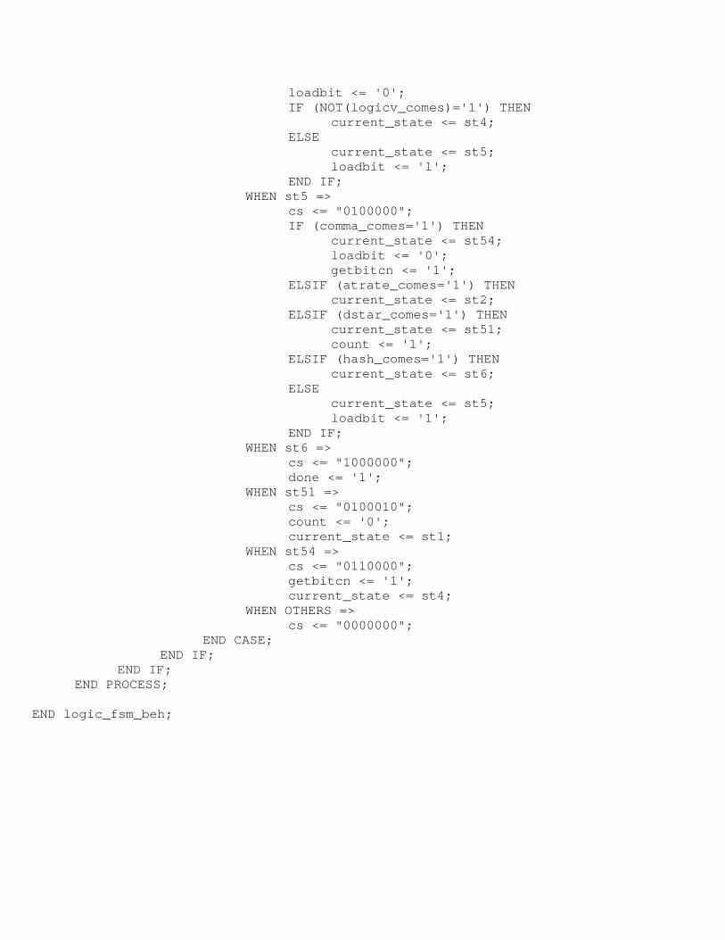
loadbit <= '0'; IF (NOT(logicv_comes)='1') THEN current_state <= st4; ELSE current_state <= st5; loadbit <= '1'; END IF; WHEN st5 => cs <= "0100000"; IF (comma_comes='1') THEN current_state <= st54; loadbit <= '0'; getbitcn <= '1'; ELSIF (atrate_comes='1') THEN current_state <= st2; ELSIF (dstar_comes='1') THEN current_state <= st51; count <= '1'; ELSIF (hash_comes='1') THEN current_state <= st6; ELSE current_state <= st5; loadbit <= '1'; END IF; WHEN st6 => cs <= "1000000"; done <= '1'; WHEN st51 => cs <= "0100010"; count <= '0'; current_state <= st1; WHEN st54 => cs <= "0110000"; getbitcn <= '1'; current_state <= st4; WHEN OTHERS => cs <= "0000000"; END CASE; END IF; END IF; END PROCESS; END logic_fsm_beh;

(ii) g++ Code for converting txt file from INCODE to matlab readable format (Back to top)
#include<fstream> #include<iostream> using namespace std; int converter(char s) { switch(s) { case '0' : return 0; case '1' : return 1; case '2' : return 2; case '3' : return 3; case '4' : return 4; case '5' : return 5; case '6' : return 6; case '7' : return 7; case '8' : return 8; case '9' : return 9; case 'A' : return 10; case 'B' : return 11; case 'C' : return 12; case 'D' : return 13; case 'E' : return 14; case 'F' : return 15; default : throw 1; } } int main(int argc,char** argv) { ++argv; --argc; ifstream IFS(argv[0]); ofstream OF1("ch1.txt"); ofstream OF2("ch2.txt"); ofstream OF3("ch3.txt"); ofstream OF4("ch4.txt"); char ch[101]; int cycle=0; while(!IFS.eof()) { IFS.getline(ch,100); for(int i=3;i<=93;i+=6) { int val=converter(ch[i]); OF4<<cycle<<"\t\t"<<(val%2)<<endl; OF3<<cycle<<"\t\t"<<((val%4)-(val%2) > 0)<<endl; OF2<<cycle<<"\t\t"<<((val%8)-(val%4) > 0)<<endl; OF1<<cycle<<"\t\t"<<((val%16)-(val%8) > 0)<<endl; cycle++; } } IFS.close(); OF1.close(); OF2.close(); OF3.close(); OF4.close(); return 0; }

(iii) Matlab Code for generating the snapshot of captured history (Back to top)
load ch1.txt; load ch2.txt; load ch3.txt; load ch4.txt; cycle = ch1(:,1); val1 = ch1(:,2); val1 = val1 + 3; val2 = ch2(:,2); val2 = val2 + 1; val3 = ch3(:,2); val3 = val3 - 1; val4 = ch4(:,2); val4 = val4 - 3; stairs(cycle,val1,'k-'); hold on; stairs(cycle,val2,'r-'); stairs(cycle,val3,'b-'); stairs(cycle,val4,'m-'); hold off; axis([0 255 -5 5]); grid on; legend('channel1','channel2','channel3','channel4','Location','SouthEast'); xlabel('Sample Number'); title('Captured history for 255 cycles after trigger generation'); (Back to top)