digital vlsi design lecture 1: introduction€¢ and provided a location for each and every gate....
TRANSCRIPT
Disclaimer: This course was prepared, in its entirety, by Adam Teman. Many materials were copied from sources freely available on the internet. When possible, these sources have been cited;
however, some references may have been cited incorrectly or overlooked. If you feel that a picture, graph, or code example has been copied from you and either needs to be cited or removed,
please feel free to email [email protected] and I will address this as soon as possible.
Digital VLSI Design
Lecture 8: Clock Tree Synthesis
Semester A, 2016-17
Lecturer: Dr. Adam Teman
22 January 2017
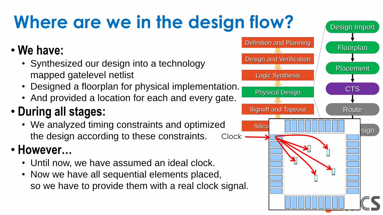
Where are we in the design flow?
• We have:• Synthesized our design into a technology
mapped gatelevel netlist
• Designed a floorplan for physical implementation.
• And provided a location for each and every gate.
• During all stages:• We analyzed timing constraints and optimized
the design according to these constraints.
• However…• Until now, we have assumed an ideal clock.
• Now we have all sequential elements placed,
so we have to provide them with a real clock signal.
Silicon Validation
Definition and Planning
Design and Verification
Logic Synthesis
Physical Design
Signoff and Tapeout
Design Import
Floorplan
Placement
CTS
Route
Finish DesignClock
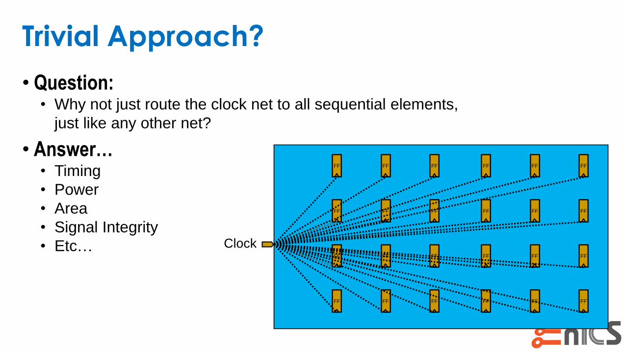
Trivial Approach?
• Question:• Why not just route the clock net to all sequential elements,
just like any other net?
• Answer…• Timing
• Power
• Area
• Signal Integrity
• Etc…
FF FF FF
FF FF FF
FF FF FF
FF FF FF
FF FF FF
FF FF FF
FF FF FF
FF FF FF
FF FF FF
FF FF FF
FF FF FF
FF FF FF
FF FF FF
FF FF FF
FF FF FF
FF FF FF
Clock
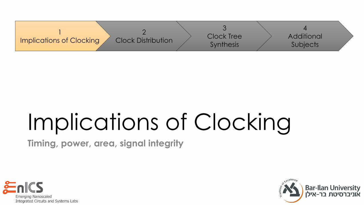
Implications of ClockingTiming, power, area, signal integrity
1
Implications of Clocking
2
Clock Distribution
3
Clock Tree
Synthesis
4
Additional
Subjects

Implications on Timing
• Let’s remember our famous timing constraints:
• Max Delay:
• Min Delay:
skew logic marginCQ SUT t t t
logic margin skewCQ holdt t t
Launch Clock
Capture Clock
Launch Clock
Capture Clock
Skew and Jitter
Implications
on Timing
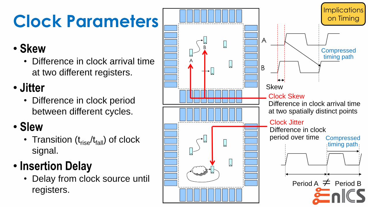
Clock Parameters
• Skew• Difference in clock arrival time
at two different registers.
• Jitter• Difference in clock period
between different cycles.
• Slew• Transition (trise/tfall) of clock
signal.
• Insertion Delay• Delay from clock source until
registers.
Clock SkewDifference in clock arrival time at two spatially distinct points
A
B
Skew
Compressed timing path
Clock JitterDifference in clock period over time
Period A Period B
Compressed timing path
Implications
on Timing
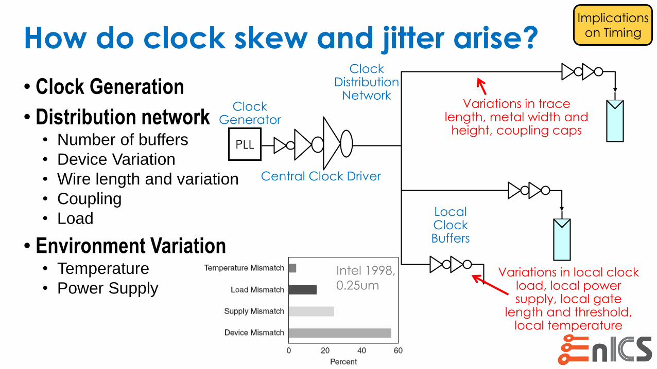
How do clock skew and jitter arise?
• Clock Generation
• Distribution network• Number of buffers
• Device Variation
• Wire length and variation
• Coupling
• Load
• Environment Variation• Temperature
• Power Supply
Central Clock Driver
Clock Distribution
Network
Local Clock Buffers
Variations in trace length, metal width and height, coupling caps
Variations in local clock load, local power supply, local gate
length and threshold, local temperature
Implications
on Timing
Intel 1998,
0.25um
PLL
Clock Generator
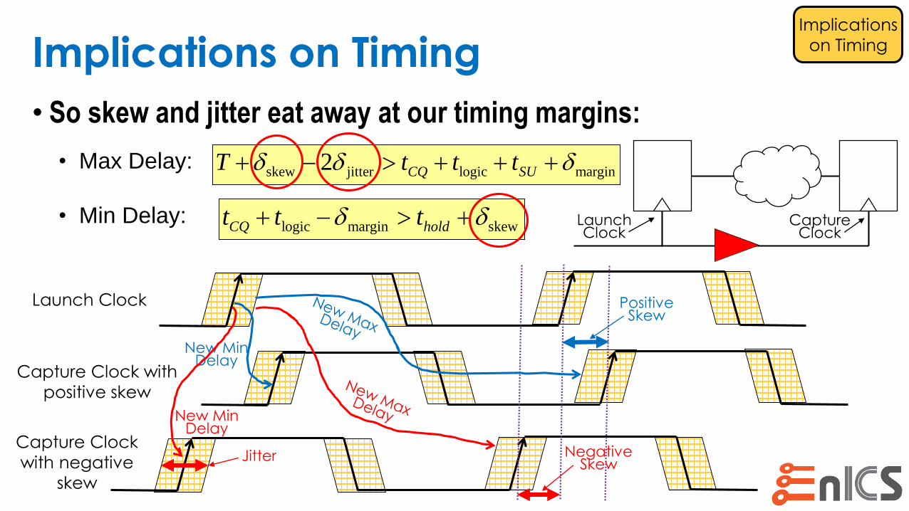
Implications on Timing
• So skew and jitter eat away at our timing margins:
• Max Delay:
• Min Delay:
skew jitter logic margin2 CQ SUT t t t
logic margin skewCQ holdt t t
Launch Clock
Capture Clock with
positive skew
Launch Clock
Capture Clock
Capture Clock
with negative
skew
Positive Skew
Negative Skew
Jitter
New Min Delay
New Min Delay
Implications
on Timing
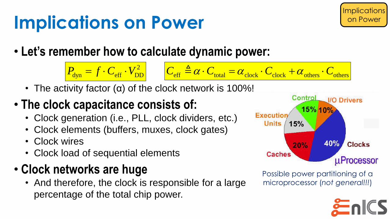
Implications on Power
• Let’s remember how to calculate dynamic power:
• The activity factor (α) of the clock network is 100%!
• The clock capacitance consists of:• Clock generation (i.e., PLL, clock dividers, etc.)
• Clock elements (buffers, muxes, clock gates)
• Clock wires
• Clock load of sequential elements
• Clock networks are huge• And therefore, the clock is responsible for a large
percentage of the total chip power.
Implications
on Power
2
dyn eff DDP f C V eff total clock clock others othersC C C C
Possible power partitioning of a
microprocessor (not general!!!)
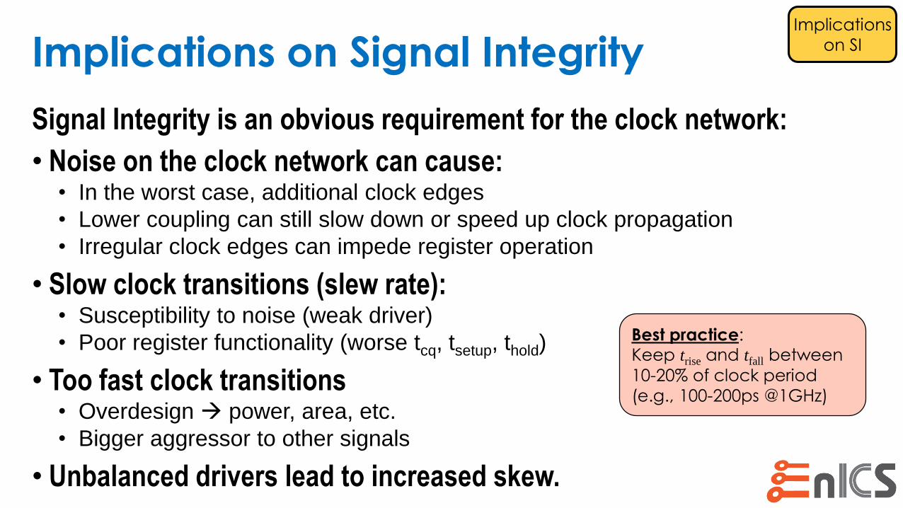
Implications on Signal Integrity
Signal Integrity is an obvious requirement for the clock network:
• Noise on the clock network can cause:• In the worst case, additional clock edges
• Lower coupling can still slow down or speed up clock propagation
• Irregular clock edges can impede register operation
• Slow clock transitions (slew rate):• Susceptibility to noise (weak driver)
• Poor register functionality (worse tcq, tsetup, thold)
• Too fast clock transitions• Overdesign power, area, etc.
• Bigger aggressor to other signals
• Unbalanced drivers lead to increased skew.
Implications
on SI
Best practice:Keep trise and tfall between
10-20% of clock period
(e.g., 100-200ps @1GHz)
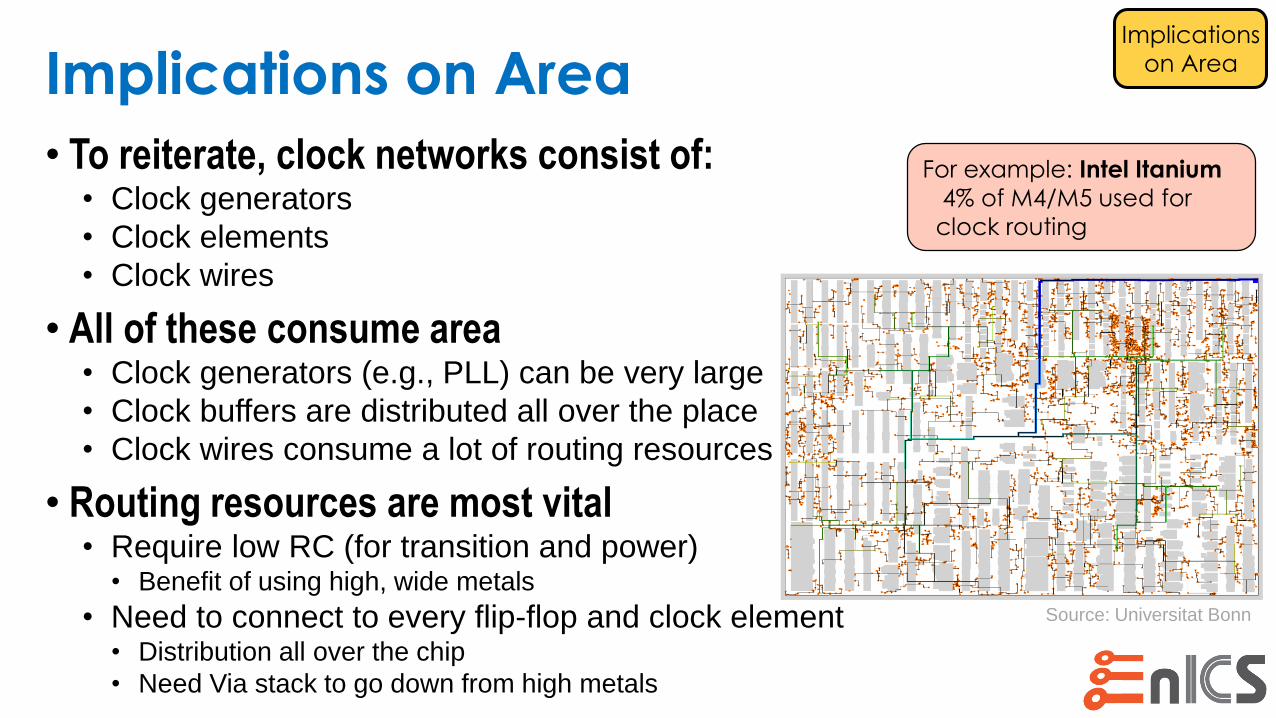
Implications on Area
• To reiterate, clock networks consist of:• Clock generators
• Clock elements
• Clock wires
• All of these consume area• Clock generators (e.g., PLL) can be very large
• Clock buffers are distributed all over the place
• Clock wires consume a lot of routing resources
• Routing resources are most vital• Require low RC (for transition and power)
• Benefit of using high, wide metals
• Need to connect to every flip-flop and clock element• Distribution all over the chip
• Need Via stack to go down from high metals
Implications
on Area
Source: Universitat Bonn
For example: Intel Itanium
4% of M4/M5 used for
clock routing
Clock DistributionSo how do we build a clock tree?
1
Implications of Clocking
2
Clock Distribution
3
Clock Tree
Synthesis
4
Additional
Subjects
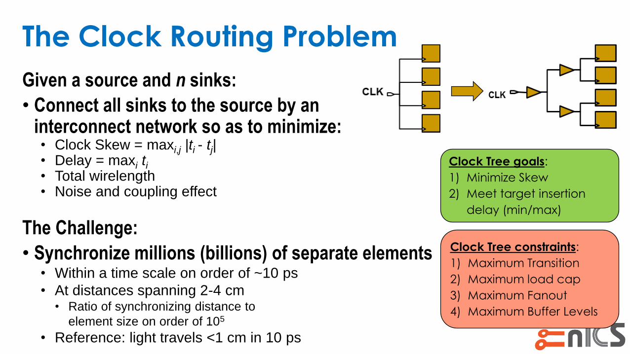
The Clock Routing Problem
Given a source and n sinks:
• Connect all sinks to the source by an interconnect network so as to minimize:• Clock Skew = maxi,j |ti - tj|• Delay = maxi ti• Total wirelength• Noise and coupling effect
The Challenge:
• Synchronize millions (billions) of separate elements• Within a time scale on order of ~10 ps
• At distances spanning 2-4 cm• Ratio of synchronizing distance to
element size on order of 105
• Reference: light travels <1 cm in 10 ps
Clock Tree goals:
1) Minimize Skew
2) Meet target insertion
delay (min/max)
Clock Tree constraints:
1) Maximum Transition
2) Maximum load cap
3) Maximum Fanout
4) Maximum Buffer Levels
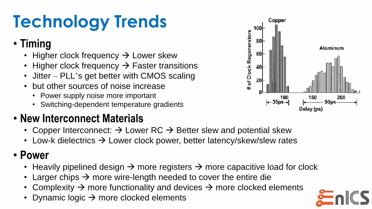
Technology Trends• Timing
• Higher clock frequency Lower skew
• Higher clock frequency Faster transitions
• Jitter – PLL’s get better with CMOS scaling
• but other sources of noise increase• Power supply noise more important
• Switching-dependent temperature gradients
• New Interconnect Materials• Copper Interconnect: Lower RC Better slew and potential skew
• Low-k dielectrics Lower clock power, better latency/skew/slew rates
• Power• Heavily pipelined design more registers more capacitive load for clock
• Larger chips more wire-length needed to cover the entire die
• Complexity more functionality and devices more clocked elements
• Dynamic logic more clocked elements
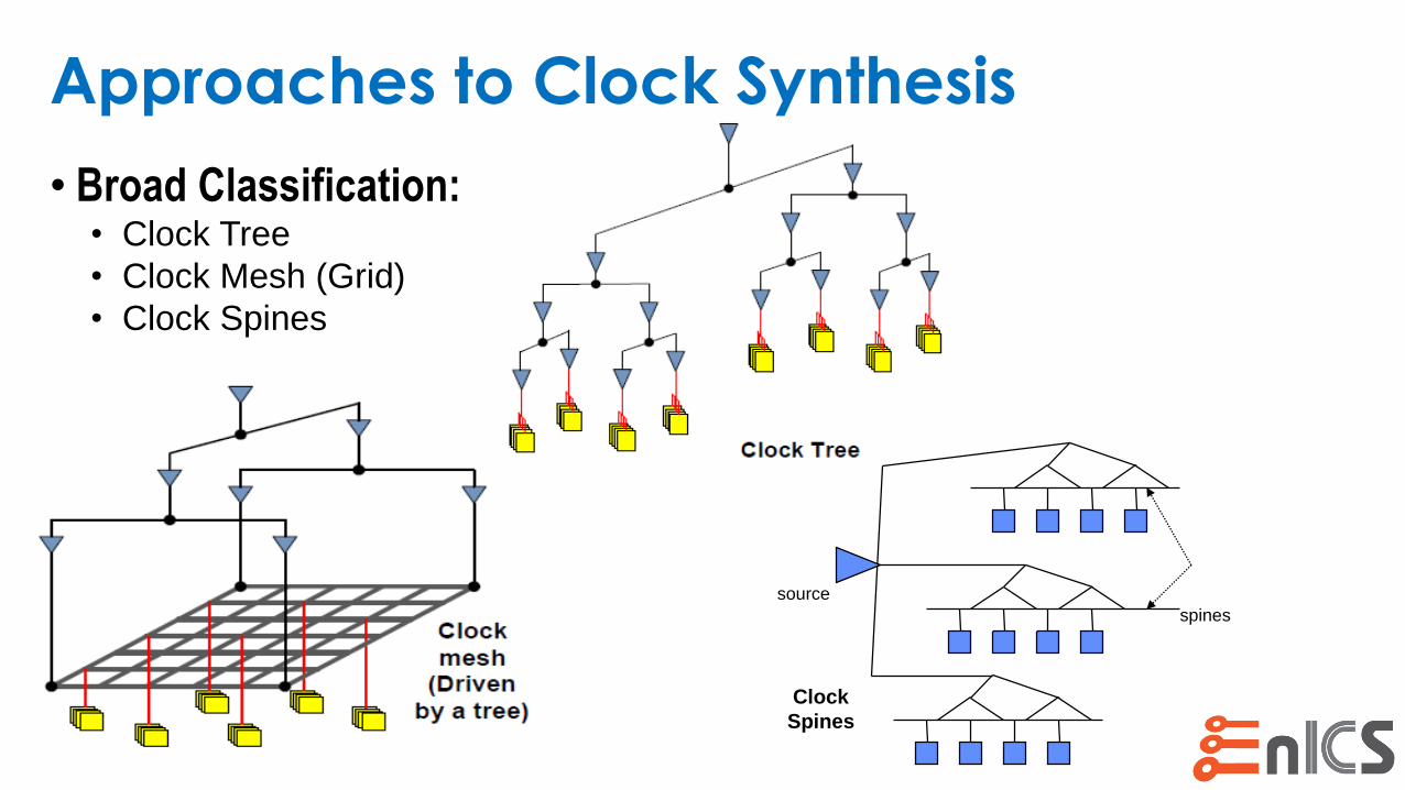
Approaches to Clock Synthesis
• Broad Classification:• Clock Tree
• Clock Mesh (Grid)
• Clock Spines
Clock
Spines
spines
source
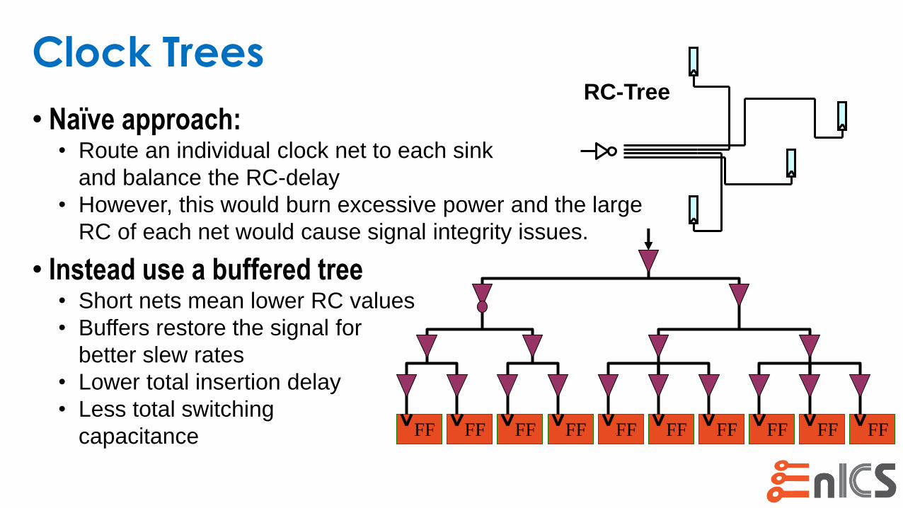
Clock Trees
• Naïve approach:• Route an individual clock net to each sink
and balance the RC-delay
• However, this would burn excessive power and the large
RC of each net would cause signal integrity issues.
• Instead use a buffered tree• Short nets mean lower RC values
• Buffers restore the signal for
better slew rates
• Lower total insertion delay
• Less total switching
capacitance FF FF FF FF FFFF FF FFFF FF
RC-Tree
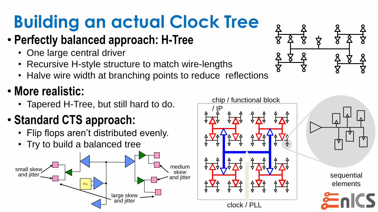
Building an actual Clock Tree• Perfectly balanced approach: H-Tree
• One large central driver
• Recursive H-style structure to match wire-lengths
• Halve wire width at branching points to reduce reflections
• More realistic:• Tapered H-Tree, but still hard to do.
• Standard CTS approach:• Flip flops aren’t distributed evenly.
• Try to build a balanced tree
clock / PLL
chip / functional block
/ IP
sequential
elementsPLL
large skew and jitter
medium skew
and jitter
small skew and jitter
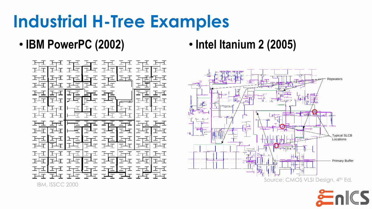
Industrial H-Tree Examples
• Intel Itanium 2 (2005)
Primary Buffer
Repeaters
Typical SLCB
Locations
Source: CMOS VLSI Design, 4th Ed.
• IBM PowerPC (2002)
IBM, ISSCC 2000
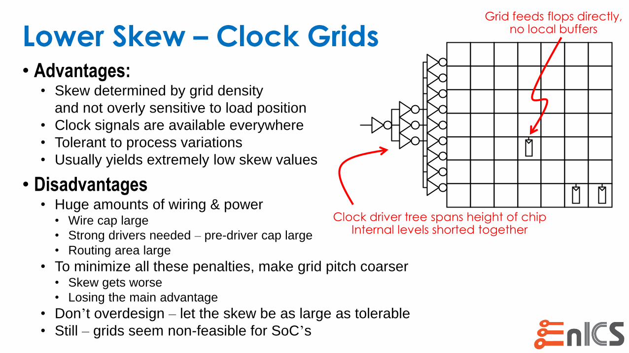
Lower Skew – Clock Grids• Advantages:
• Skew determined by grid density
and not overly sensitive to load position
• Clock signals are available everywhere
• Tolerant to process variations
• Usually yields extremely low skew values
• Disadvantages• Huge amounts of wiring & power
• Wire cap large
• Strong drivers needed – pre-driver cap large
• Routing area large
• To minimize all these penalties, make grid pitch coarser• Skew gets worse
• Losing the main advantage
• Don’t overdesign – let the skew be as large as tolerable
• Still – grids seem non-feasible for SoC’s
Grid feeds flops directly, no local buffers
Clock driver tree spans height of chipInternal levels shorted together
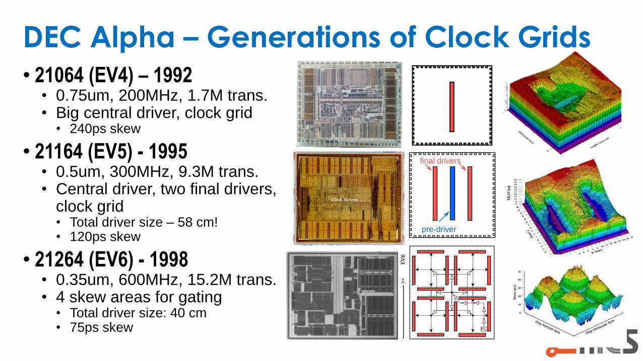
DEC Alpha – Generations of Clock Grids• 21064 (EV4) – 1992
• 0.75um, 200MHz, 1.7M trans.• Big central driver, clock grid
• 240ps skew
• 21164 (EV5) - 1995• 0.5um, 300MHz, 9.3M trans.• Central driver, two final drivers,
clock grid• Total driver size – 58 cm!• 120ps skew
• 21264 (EV6) - 1998• 0.35um, 600MHz, 15.2M trans.• 4 skew areas for gating
• Total driver size: 40 cm• 75ps skew
pre-driver
final drivers
Clock Drivers
PLL
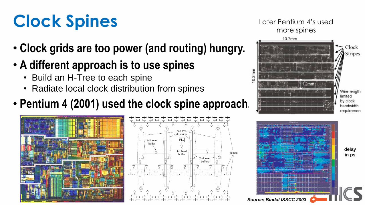
Clock Spines
• Clock grids are too power (and routing) hungry.
• A different approach is to use spines• Build an H-Tree to each spine
• Radiate local clock distribution from spines
• Pentium 4 (2001) used the clock spine approach.
Source: Bindal ISSCC 2003
delay
in ps
Later Pentium 4’s used
more spines
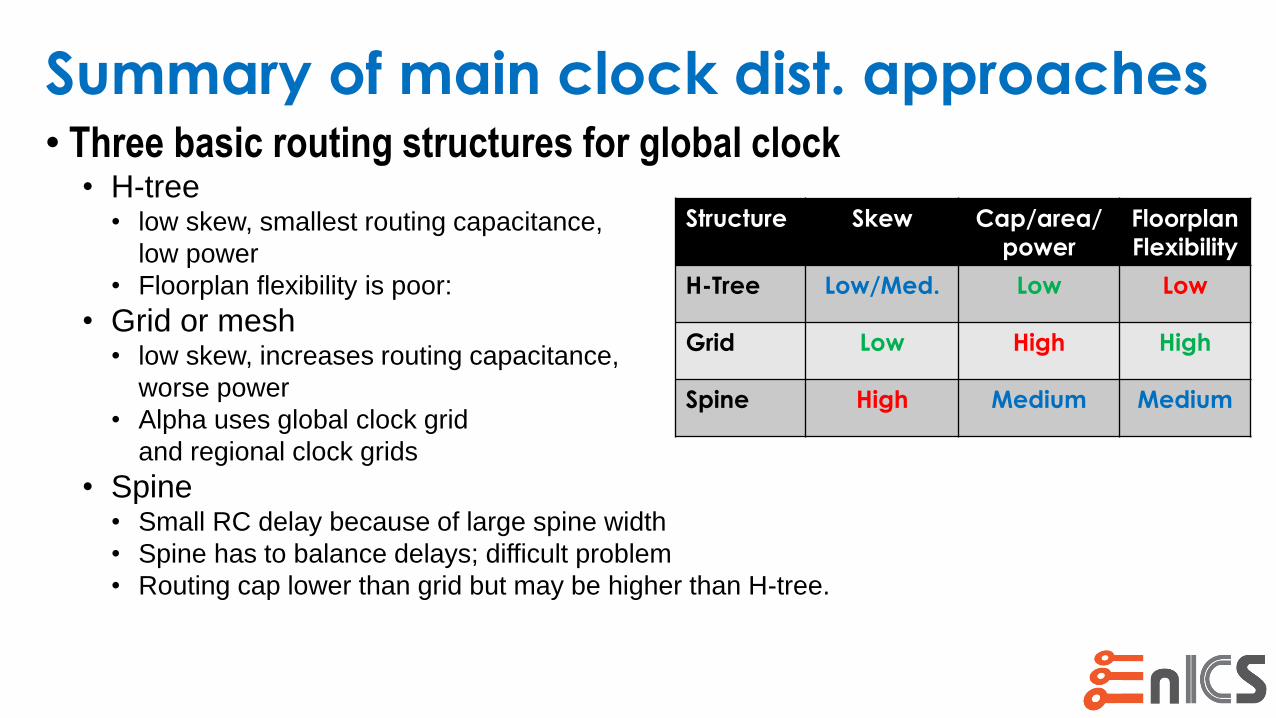
Summary of main clock dist. approaches• Three basic routing structures for global clock
• H-tree• low skew, smallest routing capacitance,
low power
• Floorplan flexibility is poor:
• Grid or mesh• low skew, increases routing capacitance,
worse power
• Alpha uses global clock grid
and regional clock grids
• Spine• Small RC delay because of large spine width
• Spine has to balance delays; difficult problem
• Routing cap lower than grid but may be higher than H-tree.
Structure Skew Cap/area/
power
Floorplan
Flexibility
H-Tree Low/Med. Low Low
Grid Low High High
Spine High Medium Medium
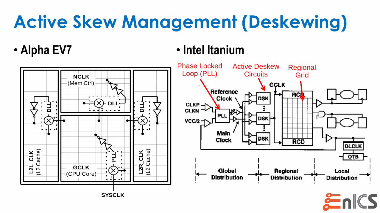
Active Skew Management (Deskewing)
• Alpha EV7
GCLK
(CPU Core)L2L
_C
LK
(L2
Cach
e)
L2R
_C
LK
(L2
Cach
e)
NCLK
(Mem Ctrl)
DLL
PL
L
SYSCLK
DL
L
DL
L• Intel Itanium
Active DeskewCircuits
Phase Locked Loop (PLL)
Regional Grid
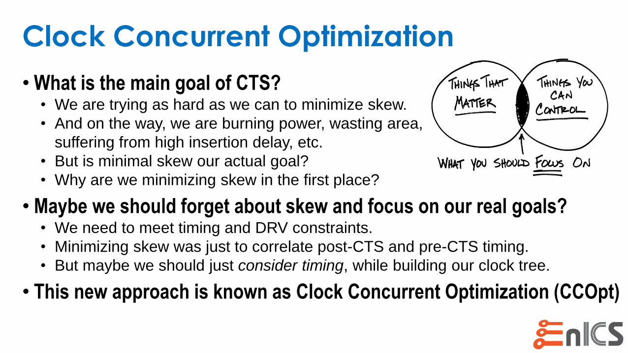
Clock Concurrent Optimization
• What is the main goal of CTS?• We are trying as hard as we can to minimize skew.
• And on the way, we are burning power, wasting area,
suffering from high insertion delay, etc.
• But is minimal skew our actual goal?
• Why are we minimizing skew in the first place?
• Maybe we should forget about skew and focus on our real goals?• We need to meet timing and DRV constraints.
• Minimizing skew was just to correlate post-CTS and pre-CTS timing.
• But maybe we should just consider timing, while building our clock tree.
• This new approach is known as Clock Concurrent Optimization (CCOpt)
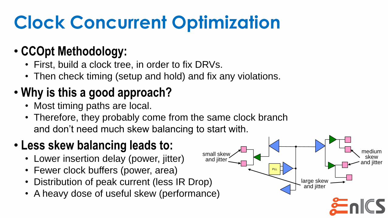
Clock Concurrent Optimization
• CCOpt Methodology:• First, build a clock tree, in order to fix DRVs.
• Then check timing (setup and hold) and fix any violations.
• Why is this a good approach?• Most timing paths are local.
• Therefore, they probably come from the same clock branch
and don’t need much skew balancing to start with.
• Less skew balancing leads to:• Lower insertion delay (power, jitter)
• Fewer clock buffers (power, area)
• Distribution of peak current (less IR Drop)
• A heavy dose of useful skew (performance)
PLL
large skew and jitter
medium skew
and jitter
small skew and jitter
Clock Tree Synthesis in EDA
1
Implications of Clocking
2
Clock Distribution
3
Clock Tree
Synthesis
4
Additional
Subjects
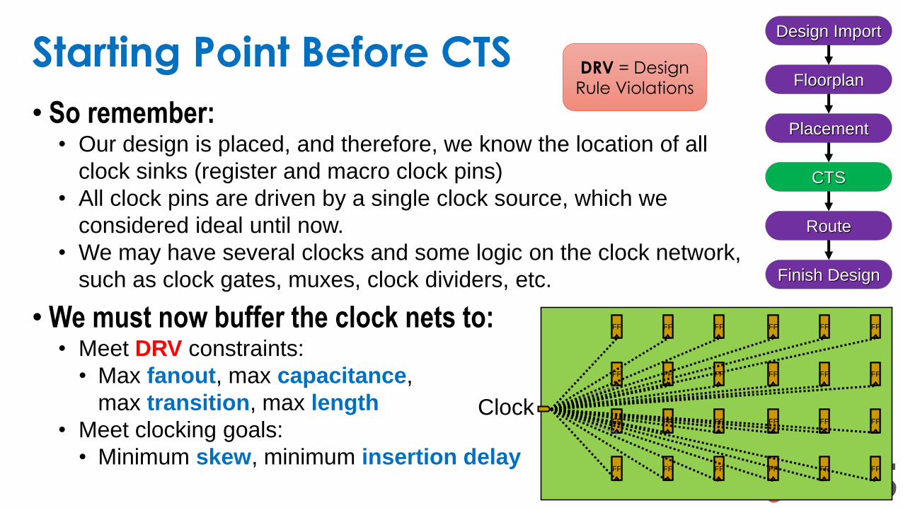
Starting Point Before CTS
• So remember:• Our design is placed, and therefore, we know the location of all
clock sinks (register and macro clock pins)
• All clock pins are driven by a single clock source, which we
considered ideal until now.
• We may have several clocks and some logic on the clock network,
such as clock gates, muxes, clock dividers, etc.
• We must now buffer the clock nets to:• Meet DRV constraints:
• Max fanout, max capacitance,
max transition, max length
• Meet clocking goals:
• Minimum skew, minimum insertion delay
FF FF FF
FF FF FF
FF FF FF
FF FF FF
FF FF FF
FF FF FF
FF FF FF
FF FF FF
FF FF FF
FF FF FF
FF FF FF
FF FF FF
FF FF FF
FF FF FF
FF FF FF
FF FF FF
Clock
Design Import
Floorplan
Placement
CTS
Route
Finish Design
DRV = Design
Rule Violations
CTS Definitions – Sources and Sinks
• Clock Source• The pin that a clock fans out from.
• This can be:• A primary input (port) to our design
• An output pin of an IP (e.g., PLL)
• An output pin of a gate
(e.g., clock mux, clock gate).
• Clock Sink• All pins that receive the clock signal.
• This can be:• Clock input of a register (FF, latch)
• Clock input of an IP (e.g., SRAM)
• Primary output (if the clock is
driven outside the block)
CLK
Clock Source –
Primary Input
CLK PLL
Clock Source –
Macro output
CLK1
CLKSEL
CLK2
Clock Source –
Gate output
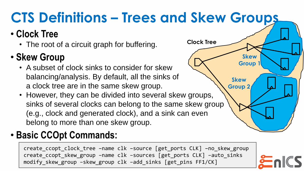
• Clock Tree• The root of a circuit graph for buffering.
• Skew Group• A subset of clock sinks to consider for skew
balancing/analysis. By default, all the sinks of
a clock tree are in the same skew group.
• However, they can be divided into several skew groups,
sinks of several clocks can belong to the same skew group
(e.g., clock and generated clock), and a sink can even
belong to more than one skew group.
• Basic CCOpt Commands:
Clock Tree
Skew
Group 1
Skew
Group 2
CTS Definitions – Trees and Skew Groups
create_ccopt_clock_tree –name clk –source [get_ports CLK] –no_skew_groupcreate_ccopt_skew_group –name clk –sources [get_ports CLK] –auto_sinksmodify_skew_group –skew_group clk –add_sinks [get_pins FF1/CK]
CTS Definitions – Stop/Ignore/Exclude Pins
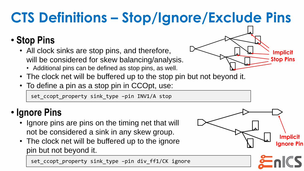
• Stop Pins• All clock sinks are stop pins, and therefore,
will be considered for skew balancing/analysis.• Additional pins can be defined as stop pins, as well.
• The clock net will be buffered up to the stop pin but not beyond it.
• To define a pin as a stop pin in CCOpt, use:
• Ignore Pins• Ignore pins are pins on the timing net that will
not be considered a sink in any skew group.
• The clock net will be buffered up to the ignore
pin but not beyond it.
set_ccopt_property sink_type –pin INV1/A stop
set_ccopt_property sink_type –pin div_ff1/CK ignore
Implicit
Stop Pins
Implicit
Ignore Pin
CTS Definitions – Stop/Ignore/Exclude Pins
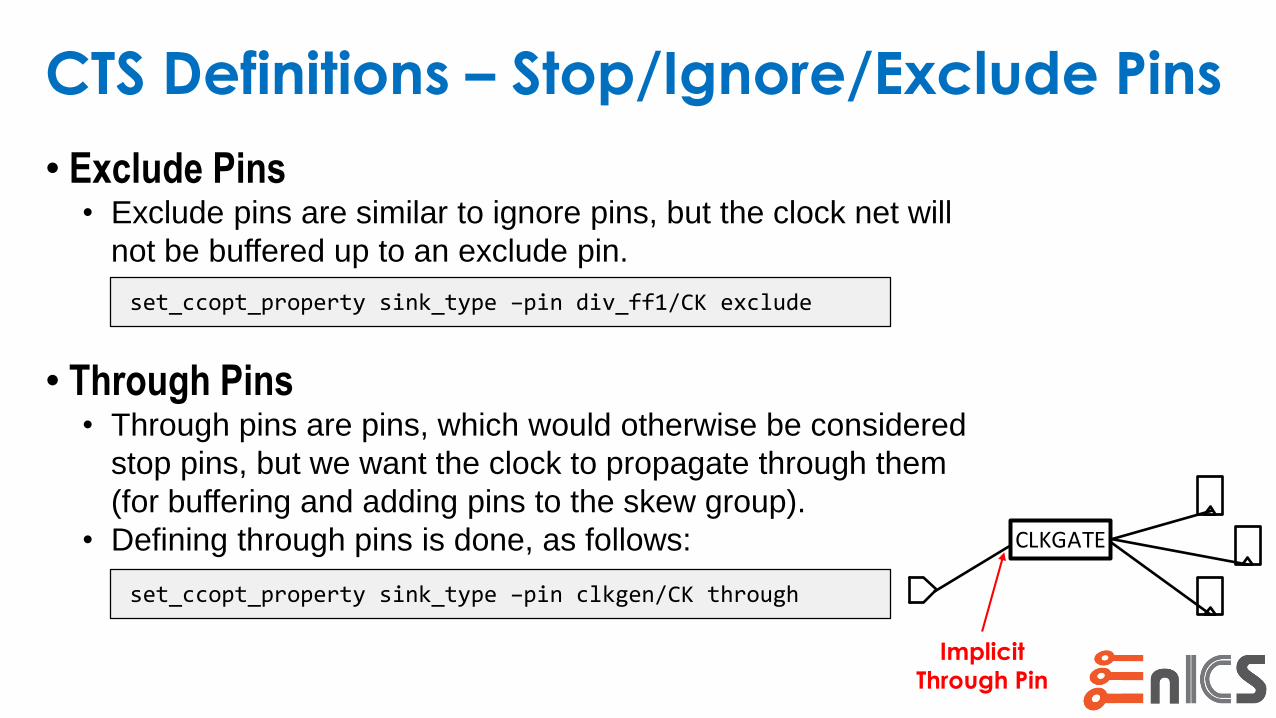
• Exclude Pins• Exclude pins are similar to ignore pins, but the clock net will
not be buffered up to an exclude pin.
• Through Pins• Through pins are pins, which would otherwise be considered
stop pins, but we want the clock to propagate through them
(for buffering and adding pins to the skew group).
• Defining through pins is done, as follows:
set_ccopt_property sink_type –pin div_ff1/CK exclude
set_ccopt_property sink_type –pin clkgen/CK through
CLKGATE
Implicit
Through Pin
CTS Definitions – Insertion Delay Pin
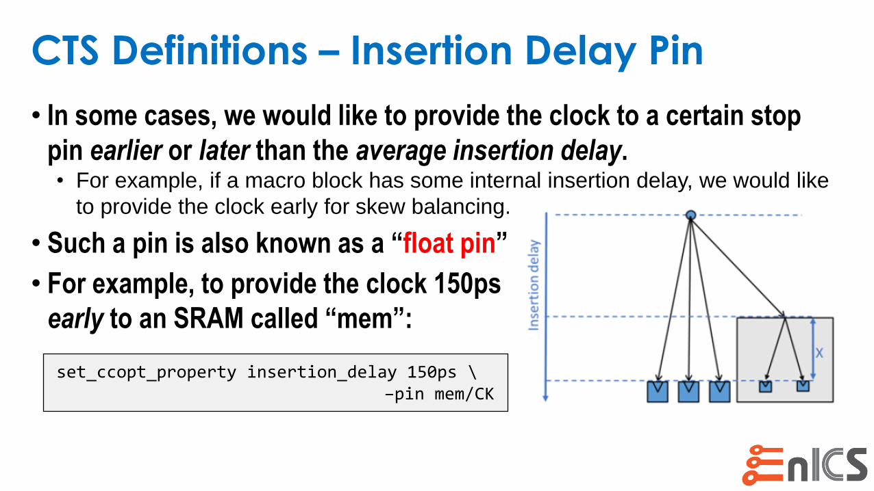
• In some cases, we would like to provide the clock to a certain stop
pin earlier or later than the average insertion delay.• For example, if a macro block has some internal insertion delay, we would like
to provide the clock early for skew balancing.
• Such a pin is also known as a “float pin”
• For example, to provide the clock 150ps
early to an SRAM called “mem”:
set_ccopt_property insertion_delay 150ps \–pin mem/CK
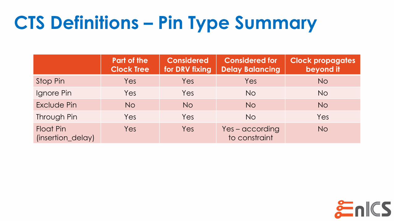
CTS Definitions – Pin Type Summary
Part of the
Clock Tree
Considered
for DRV fixing
Considered for
Delay Balancing
Clock propagates
beyond it
Stop Pin Yes Yes Yes No
Ignore Pin Yes Yes No No
Exclude Pin No No No No
Through Pin Yes Yes No Yes
Float Pin
(insertion_delay)
Yes Yes Yes – according
to constraint
No
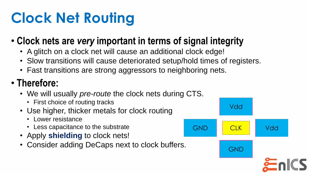
Clock Net Routing
• Clock nets are very important in terms of signal integrity• A glitch on a clock net will cause an additional clock edge!
• Slow transitions will cause deteriorated setup/hold times of registers.
• Fast transitions are strong aggressors to neighboring nets.
• Therefore:• We will usually pre-route the clock nets during CTS.
• First choice of routing tracks
• Use higher, thicker metals for clock routing • Lower resistance
• Less capacitance to the substrate
• Apply shielding to clock nets!
• Consider adding DeCaps next to clock buffers.
Vdd
GND
GND VddCLK
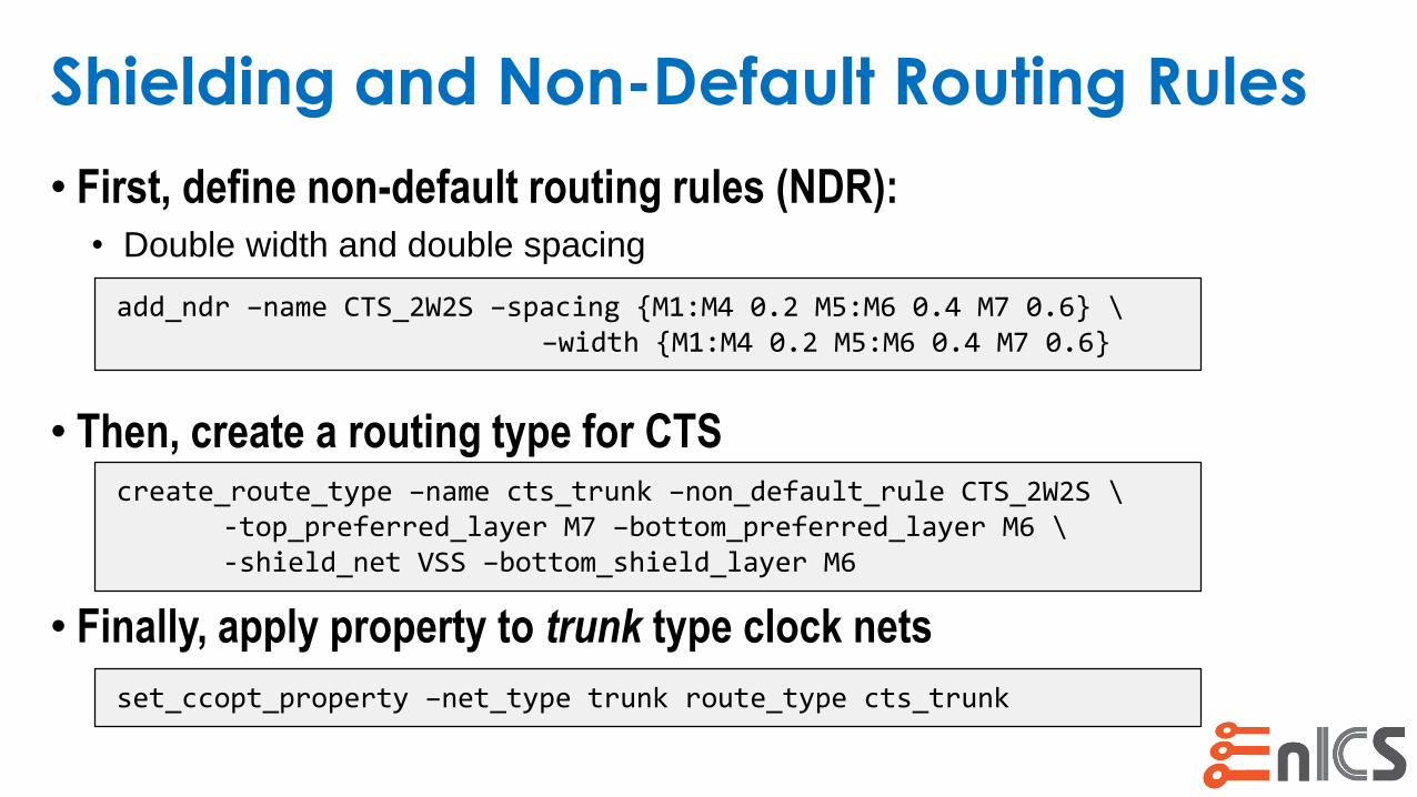
Shielding and Non-Default Routing Rules
• First, define non-default routing rules (NDR):• Double width and double spacing
• Then, create a routing type for CTS
• Finally, apply property to trunk type clock nets
add_ndr –name CTS_2W2S –spacing {M1:M4 0.2 M5:M6 0.4 M7 0.6} \–width {M1:M4 0.2 M5:M6 0.4 M7 0.6}
set_ccopt_property –net_type trunk route_type cts_trunk
create_route_type –name cts_trunk –non_default_rule CTS_2W2S \-top_preferred_layer M7 –bottom_preferred_layer M6 \-shield_net VSS –bottom_shield_layer M6
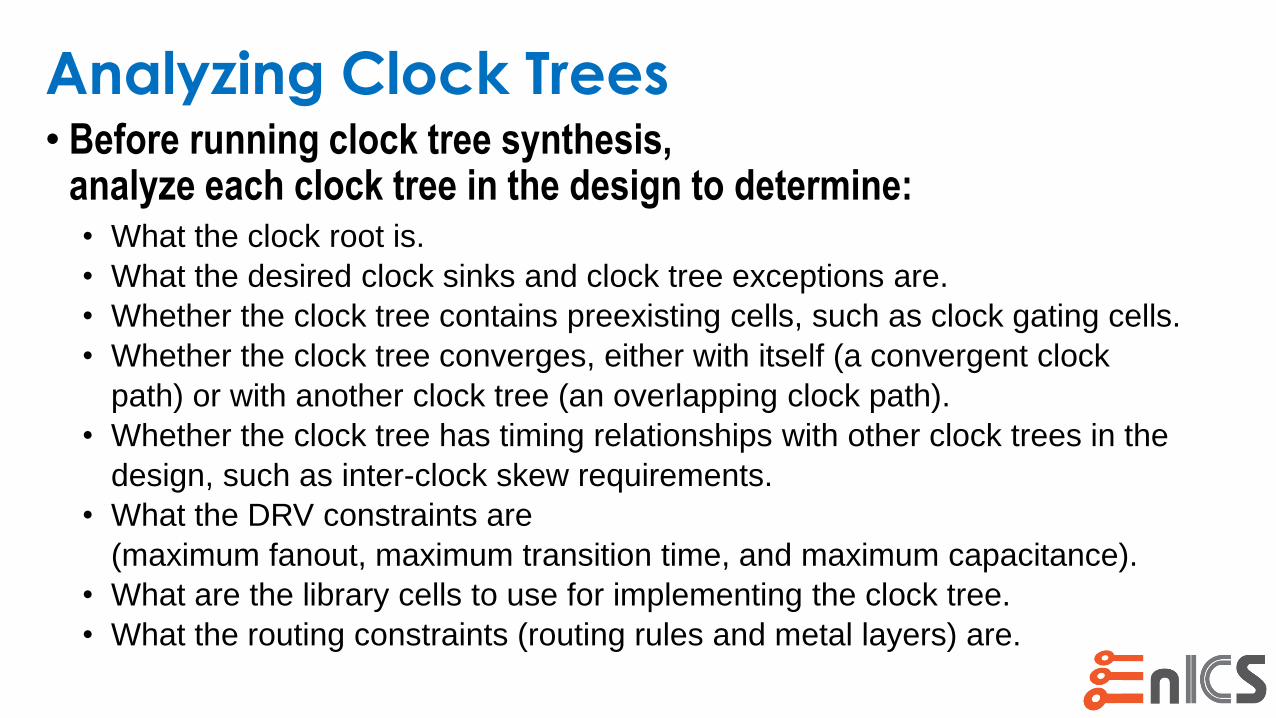
Analyzing Clock Trees• Before running clock tree synthesis,
analyze each clock tree in the design to determine:• What the clock root is.
• What the desired clock sinks and clock tree exceptions are.
• Whether the clock tree contains preexisting cells, such as clock gating cells.
• Whether the clock tree converges, either with itself (a convergent clock
path) or with another clock tree (an overlapping clock path).
• Whether the clock tree has timing relationships with other clock trees in the
design, such as inter-clock skew requirements.
• What the DRV constraints are
(maximum fanout, maximum transition time, and maximum capacitance).
• What are the library cells to use for implementing the clock tree.
• What the routing constraints (routing rules and metal layers) are.
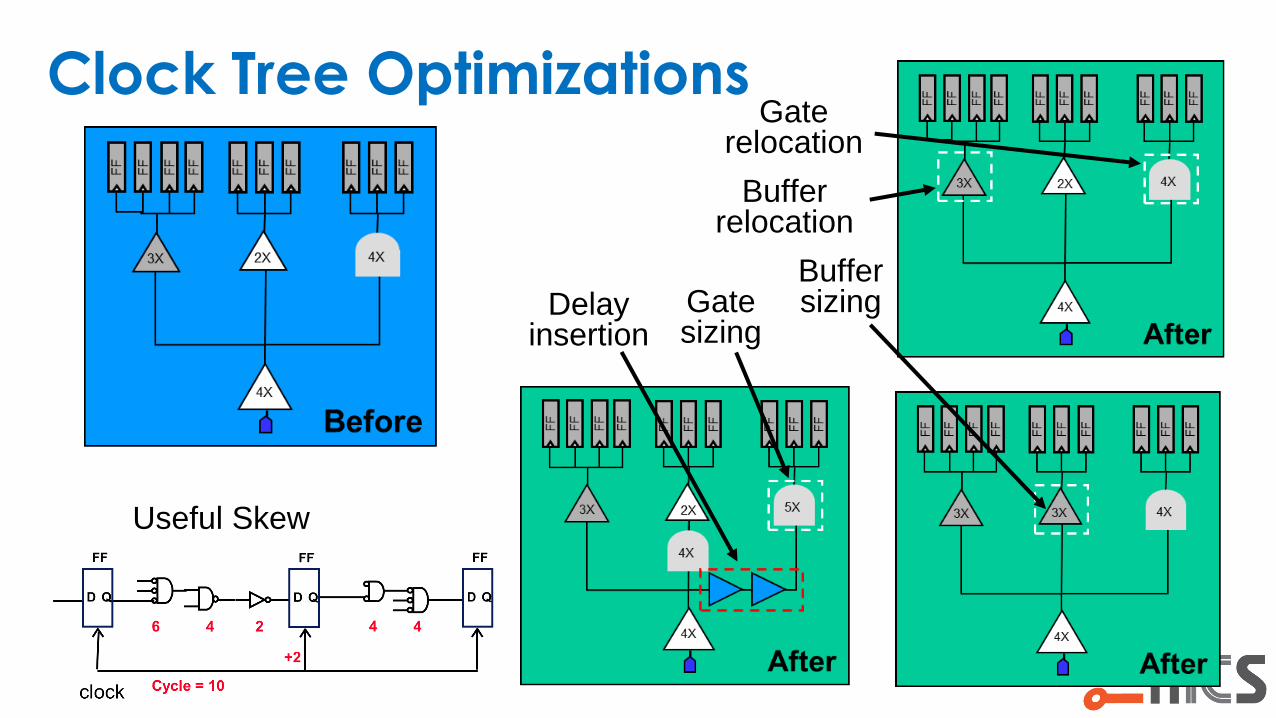
Clock Tree Optimizations
Buffer sizingGate
sizingDelay
insertion
Gate relocation
Buffer relocation
Useful Skew
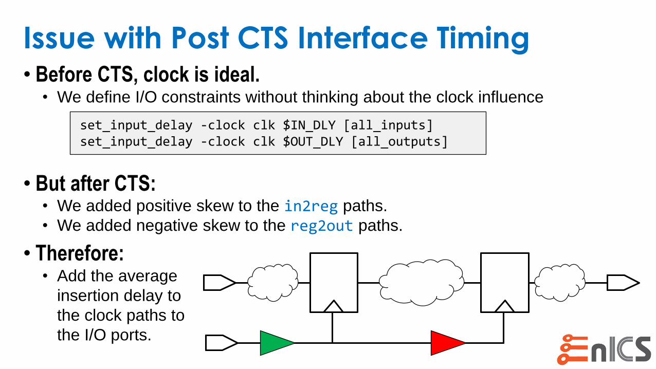
Issue with Post CTS Interface Timing• Before CTS, clock is ideal.
• We define I/O constraints without thinking about the clock influence
• But after CTS:• We added positive skew to the in2reg paths.
• We added negative skew to the reg2out paths.
• Therefore:• Add the average
insertion delay to
the clock paths to
the I/O ports.
set_input_delay -clock clk $IN_DLY [all_inputs]set_input_delay -clock clk $OUT_DLY [all_outputs]
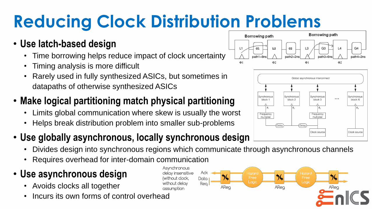
Reducing Clock Distribution Problems• Use latch-based design
• Time borrowing helps reduce impact of clock uncertainty
• Timing analysis is more difficult
• Rarely used in fully synthesized ASICs, but sometimes in
datapaths of otherwise synthesized ASICs
• Make logical partitioning match physical partitioning• Limits global communication where skew is usually the worst
• Helps break distribution problem into smaller sub-problems
• Use globally asynchronous, locally synchronous design• Divides design into synchronous regions which communicate through asynchronous channels
• Requires overhead for inter-domain communication
• Use asynchronous design• Avoids clocks all together
• Incurs its own forms of control overhead
Main References
• Berkeley EE141
• Rabaey “Digital Integrated Circuits”
• Synopsys University Courseware
• IDESA
• Gil Rahav
• Dennis Sylvester, UMICH
• MIT 6.375 Complex Digital Systems
• Horowitz, Stanford