digital vlsi lab assignment 1 - · pdf filedigital vlsi lab assignment 1 ... between manual...
TRANSCRIPT

DIGITAL VLSI
LAB ASSIGNMENT 1
Problem 1: NMOS and PMOS plots using Cadence.
In this exercise, you are required to generate both NMOS and PMOS I-V device characteristics (I/P and O/P) using Cadence (Use 65nm process Technology). Plot your results. Compare the current levels for the two devices in saturation when they are minimum sized.
Now connect the PMOS and NMOS transistors to form a CMOS inverter. Plot the voltage transfer characteristics, and observe the variation by varying the pull-up to pull-down device ratios. Please report the width of the PMOS for which symmetric switching is achieved. Calculate the Noise Margin in the form of NML and NMH from plot.
Solution:
NMOS: N type MOSFET is form by taking p substrate and two high doped n is diffused in this p substrate. These two are taking as drain and source. Between drain and source channel is formed. NMOS is in the cut off region when gate to source voltage (Vgs) is negative. So for enhancement mode Vgs is greater than threshold voltage.
Doing in cadence we give positive supply to gate and drain. Value of this positive supply is 1.2V (Because we are working in 65nm process technology so that the maximum supply voltage is 1.2V). we do the analysis in the range of 0 to 1.2V.
Schematic diagram of NMOS in Cadence

Two different types of analysis:
1) Curve B/W Id and Vds Taking Vgs constant (1.2V). (Output characteristics). It comes in 1st quadrant.
2). Curve B/W Id and Vgs Taking Vds constant(1.2V) (Input characteristics). This comes in 1st quadrant.

PMOS:
PMOS is behaving just opposite to NMOS. PMOS is made by taking N type substrate and doped TWO high doped P in N type substrate. PMOS is working when gate to source voltage is negative. So in this analysis we apply negative voltage to gate and drain. Also do it analysis to -1.2 to 0.
Schematic of PMOS in cadence
We do analysis of two types:
1). Curve B/W Id and Vds Taking Vgs constant. (Output characteristics)
This curve is B/W Id and Vds for different values of Vgs (-1.2 to 0 linear steps 4). Values of Vgs is varies by taking a variable and do it simulation. Characteristic is come 3rd quadrant.

2). Curve B/W Id and Vgs Taking Vds constant.( input characteristics)
This curve is B/W Id and Vgs for different values of Vds (-1.2 to 0 linear steps 4). The characteristic is come 3rd quadrant.
CMOS INVERTER:
CMOS INVERTER is combination of NMOS and PMOS. NMOS is used as a pull down system and PMOS is used as a pull up system. The output is inverse of the input which is given to CMOS inverter. In CMOS we give Vgs and Vds as 1.2V. In B/W the NMOS and PMOS we take the output.

Schematic of CMOS Inverter:
We analysis the transfer characteristics.( Vout v/s Vin ).
Then take a variable which varies the width of PMOS and do the analysis where symmetric switching is obtained (at symmetric switching Vin=Vout= Vdd/2 is occur so we at that width ratio which is nearest to this point).
Transfer characteristics:

I take a variable PMOS width=w and sweep it firstly 0 to 4 and then i plot a graph than for exact calculation i take w= 2.5 to 2.75 and sweep it taking linear step of 6. Then I found for approximate symmetric switching I get 2.625 width ratio of PMOS to NMOS.
Approximate switching width ratio 2.625. For Noise margin we take the points where slope -1 and 1. We take that point and calculate the noise margin:

Where slope is -1.
Voh=Vout = 1.06 V
Vil=Vin= 0.514
Where slope is 1
Vol=Vout=.129
Vin=0.68V
Noise margin Nlow
Noise Margin Nhigh
2. (a) Analyze and plot Vout vs. Vin with Vin varying from 0 to 1.2 volts (use steps of 0.25 V) for the MOS circuit shown below. Consider VDD= 1.2 V.
(b) Repeat (a) using Cadence.
c) Repeat (a) and (b) using a MOS transistor with (W/L) = 3/1. While doing so, vary the resistance values and report the results for 16K, 32K, and 64K Ohms. Is the discrepancy between manual and computer analysis larger or smaller (perform hand calculations for only resistance 64K)? Explain why. Also plot the voltage transfer characteristics and comment on noise margins. Can this circuit be used as an inverter?
Solution:
Using Cadence: firstly I do with 8K resistor and draw the transfer characteristics
Schematic characteristic:

vgs
i take Vgs and vds is equal to 1.2V and do simple analysis by which i can get transfer charcterstics of this circuit.

Transfer Characteristics for taking Vout v/s Vin taking Step Size of Vin is 0.25:
For question (c) change the width ratio by 3/1 mean width of NMOS is multiplied by 3. And take the resistor as a variable and varies it from 8 to 64 by taking times stepping of 2. So we get these types of transfer characteristics graph for 8K, 16K, 32K, 64K ohm resistor. also take Vds is taking in step size of 0.25.
As the resistance increases switching characteristics is decreases mean 64K is most away from its switching characteristics. As the resistance increases graph goes down.
No this circuit can’t be used as inverter because for 8K ohm resistor Vout does not goes to Zero. As the resistance increases Vout goes towards to zero. But not exact to be zero. So this circuit cannot behave like inverter.

(a).manual calculation of a and c part:

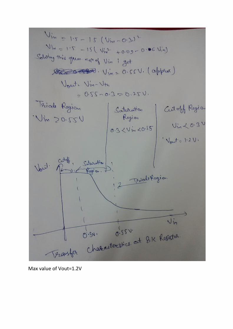
Max value of Vout=1.2V
