diluted magnetic semiconductor resonant tunneling structures …praveens/spintronics... ·...
TRANSCRIPT

Diluted magnetic semiconductorResonant Tunneling Structures
for spin manipulation
A Thesis submitted for the degreeof Doctor of Philosophy
Bavarian Julius–Maximilians–UniversitatWurzburg
submitted by
Anatoliy Slobodskyy
Wurzburg, February 2005

Submitted: . . . . . . . . . . . . . . . . . . . . . . . . . . . . . . . . . . . . . . . . . . .
Faculty of physic and astronomy
1. Supervisor: Prof. Dr. L.W. Molenkamp
for the dissertation
1. Prufer:
2. Prufer:
for oral exam
Day of the oral exam: . . . . . . . . . . . . . . . . . . . . . . . . . . . . . . . . .
Doktorurkunde ausgehandigt am: . . . . . . . . . . . . . . . . . . . . . .

Contents
1 Introduction. 1
1.1 Spin electronics. . . . . . . . . . . . . . . . . . . . . . . . . . . . . . . . . . . 1
1.2 Spin injection and manipulation. . . . . . . . . . . . . . . . . . . . . . . . . . 3
1.3 Spin detection. . . . . . . . . . . . . . . . . . . . . . . . . . . . . . . . . . . 4
2 Theory of Resonant tunneling. 7
2.1 Resonant tunneling. . . . . . . . . . . . . . . . . . . . . . . . . . . . . . . . . 7
2.1.1 Basics of resonant tunneling. . . . . . . . . . . . . . . . . . . . . . . . 7
2.1.2 Coherent versus incoherent resonant tunneling process. . . . . . . . . . 16
2.1.3 Elastic and inelastic scattering mechanisms, phonon replica. . . . . . . 20
2.2 Magnetic field influence on RTDs. . . . . . . . . . . . . . . . . . . . . . . . . 22
2.2.1 Magnetic field perpendicular to the QW. . . . . . . . . . . . . . . . . . 22
2.2.2 Magnetic field in-plane of the QW. . . . . . . . . . . . . . . . . . . . . 24
3 Experiment. 27
3.1 Diluted magnetic semiconductors. . . . . . . . . . . . . . . . . . . . . . . . . 27
3.1.1 Giant Zeeman splitting. . . . . . . . . . . . . . . . . . . . . . . . . . . 27
3.1.2 [Zn,Be,Mn]Se DMS. . . . . . . . . . . . . . . . . . . . . . . . . . . . 29

iv CONTENTS
3.2 Setup and sample design. . . . . . . . . . . . . . . . . . . . . . . . . . . . . . 32
3.2.1 Measurement setup and technique. . . . . . . . . . . . . . . . . . . . . 32
3.2.2 Charges in a RTD. . . . . . . . . . . . . . . . . . . . . . . . . . . . . 33
3.2.3 Multistabilities in resonant tunneling structures. . . . . . . . . . . . . . 34
3.2.4 Sample design. . . . . . . . . . . . . . . . . . . . . . . . . . . . . . . 37
4 Spin selection in RTDs with magnetic QW. 39
4.1 Introduction. . . . . . . . . . . . . . . . . . . . . . . . . . . . . . . . . . . . . 39
4.2 Details of the experiment. . . . . . . . . . . . . . . . . . . . . . . . . . . . . . 41
4.3 Results and simulation of spin resolved current through the device. . . . . . . . 42
4.4 Summary. . . . . . . . . . . . . . . . . . . . . . . . . . . . . . . . . . . . . . 47
5 RTD with magnetic QW as a spin detector. 49
5.1 Spin polarization at high magnetic field. . . . . . . . . . . . . . . . . . . . . . 49
5.2 Influence of spin-polarized current on RTDs I-V characteristics. . . . . . . . . 50
5.3 Temperature dependence of the effect. . . . . . . . . . . . . . . . . . . . . . . 53
6 Double RTD with magnetic QWs for current spin polarization and detection. 57
7 RTD with magnetic injector or barriers for spin manipulation. 61
7.1 Introduction and the magnetic injector sample design. . . . . . . . . . . . . . . 61
7.2 Magnetic field induced change of I-V characteristic of RTD structure with mag-netic injector. . . . . . . . . . . . . . . . . . . . . . . . . . . . . . . . . . . . 63
7.3 Explanation of magnetic field influence on the transport in RTD with magneticinjector. . . . . . . . . . . . . . . . . . . . . . . . . . . . . . . . . . . . . . . 64
7.4 RTD with magnetic barriers for spin manipulation. . . . . . . . . . . . . . . . 67

CONTENTS v
8 Spin resolved resonant tunneling in self-assembled quantum dots. 71
8.1 Self-Assembled II-V Quantum Dot as a Voltage-Controlled Spin-Filter. . . . . 71
8.2 Sample and measurements details. . . . . . . . . . . . . . . . . . . . . . . . . 72
8.3 Magnetic field evolution of the resonance peaks. . . . . . . . . . . . . . . . . . 73
8.4 Understanding the effect of an external magnetic field. . . . . . . . . . . . . . 75
Summary 79
Zusammenfassung 83
Bibliograhy 95

vi CONTENTS

Chapter 1
Introduction.
1.1 Spin electronics.
Spin electronics, or in short spintronics, is a multidisciplinary field whose central theme is theactive manipulation of the freedom of spin degree of charge carriers in solid-state systems. Thegeneration of spin polarization usually means creating a nonequilibrium spin population. Thiscan be achieved in several ways. Traditionally, spin has been oriented using optical techniquesin which circularly polarized photons transfer their angular momenta to electrons, for deviceapplications, however, electrical spin injection is more desirable. In electrical spin injection, amagnetic electrode is connected to the sample. When the current drives spin-polarized electronsfrom the electrode to the sample, nonequilibrium spin accumulates at the interface. The rate ofspin accumulation is decreased by spin relaxation, the process of bringing the accumulated spinpopulation back to equilibrium.
Injection and detection of a spin-polarized current in semiconductors was successfully demon-strated by R. Fiederling et al. [FKR+99], achieving a high spin injection efficiency of more than90% as detected by electroluminescence emitted from a [Al,Ga]As light-emitting diode (LED).The experiment was carried out with a [Zn,Be,Mn]Se spin aligner to inject polarized electronsinto the diode (LED).
A step towards understanding the process of electrical spin injection was made by G. Schmidtet al. [SFM+00]. They showed that the very low efficiency of electrical spin injection from fer-romagnetic metals into semiconductor is explained in terms of conductance mismatch. In thenonmagnetic semiconductor, the conductance of both spin channels is identical and the differ-ence in the conductance of spin channels in ferromagnetic metal causes the spin-polarization ofthe current. Due to a large conductance mismatch between metal and semiconductor, electrontransport through the spin channels is totally dominated by the conductance of semiconductor.This fact limits the use of ferromagnetic metals as a material for spintronics, not only because ofthe relatively low ∼ 45% spin-polarization of carriers within the ferromagnet, but also because

2 Introduction.
of the low resistance of the spin injecting metal as compared to the semiconductor into whichthe spin-polarized electrons are to be injected.
Although, ferromagnetic metals have a high Curie temperature which gives possibility for spinmanipulation at room temperature without external magnetic field. An effective way to over-come the conductivity mismatch problem is to use 100% spin-polarized materials. One of thepromising families of materials in this sense, are half metals, Heusler alloys [dGMvE83]. Halfmetal means that the only available states at the Fermi level in these materials are spin-polarized,resulting in 100% spin polarization. Moreover, the materials are ferromagnetic at room temper-atures.
Another big issue in the field of spintronics in recent years is to design new ferromagnetic semi-conductor materials with room temperature ferromagnetism. In order to achieve ferromagneticbehaviour, semiconductors are diluted with magnetic ions to make diluted magnetic semicon-ductors (DMS). The advantage of DMS, compared to metals, is that conductivity of the injectoris similar to that of the nonmagnetic semiconductor used in applications, and in this way theconductance mismatch problem can be overcome.
Applications of spin electronics are successfully used in the ”read” heads for magnetic harddisk drives, because of extreme sensitivity to external magnetic field. The effect used is knownas giant magnetoresistance (GMR) [BBF+88] and results from the effect of the scattering ofelectrons on the interface of alternate ferromagnetic/paramagnetic layers. Depending on parallelor anti-parallel orientation of the layers, the resistance of the structure will be changed. Theinterfaces are normally used with a tunnel barrier in order to increase the effect and are calledtunneling magnetoresistance (TMR). At the same time, GMR based random access memory(RAM), magnetic random access memory (MRAM), and computer hard disks are under rapiddevelopment.
A long-term goal for spintronics applications is quantum computation [LD98, Kan98]. Thequantum algorithms require that the internal state of the quantum computer will be controlledwith extraordinary precision, so that the coherent quantum state, upon which the quantum algo-rithms rely, is not destroyed.
In this thesis, we will discuss our recent results of measurements and simulation of magneticRTD structures as possible applications for semiconductor spintronics. The thesis is organizedas follows: In chapter 1 we discuss the principles of spin injection and manipulation. Chapter 2reviews the theory of resonant tunneling. In chapter 3 we describe the details of the experiment.In the subsequent chapters we show our experiment results on spin selection (chapter 4) andspin detection (chapter 5), in all-II-VI RTD with magnetic QW, a two parallel RTD system(chapter 6), spin manipulation with RTDs with magnetic injector or barriers (chapter 7), andspin resolved resonant tunneling in self-assembled quantum dots (chapter 8). An overview ofthe results is presented as the summary. Finally, we present related results on ”Spin Injection inthe Nonlinear Regime: Band Bending Effects” as an appendix.

1.2 Spin injection and manipulation. 3
1.2 Spin injection and manipulation.
In 1990, Datta and Das proposed a design for a spin-polarized field-effect transistor, or SFET[DD90]. In a conventional FET, a narrow semiconductor channel runs between two electrodes- source and drain. When voltage is applied to the gate electrode, which is above the channel,the resulting electric field drives electrons out of the channel (for instance), turning the channelinto an insulator. The Datta-Das spin FET has a spin-polarizer source and drain so that thecurrent flowing into the channel is spin-polarized. When a voltage is applied to the gate, thespins rotate as they pass through the channel and the drain rejects these anti-aligned electrons.Naturally, in order to achieve proper spin selectivity at the drain, transport of the carriers mustbe quantum mechanically coherent. Flipping an electron’s spin takes much less energy andcan be done much faster than pushing an electron out of the channel. One can also imaginechanging the orientation of the source or drain with a magnetic field, introducing an additionaltype of control: logic gates whose functions can be changed on the fly.
One of the most important and at the same time most complicated tasks in such kind of devices isto inject and manipulate spin-polarized electric current in the nonmagnetic media. Using DMSor Heusler alloys not necessarily means that 100% of spin-polarized current can be injected,because of the scattering on interface states. High electric-field diffusive regime, which has noanalogue in metals, was shown to improve the spin injection efficiency [YF02]. The idea is thatat reasonably high electric-fields, the spin-diffusion lengths will be different for different spinoriented currents. The enhancement of the spin injection efficiency also occurs for high electric-field spin injection through a spin-selective interfacial barrier. Additional interface effects andeffects of band bending are analysed in [SGG+04].
There are many options to manipulate spin within the NMS. One of the effects being exploredin order to manipulate spin within the material is the fact that in the presence of an electric field,the spin and momentum states of an electron can be coupled; this is known as spin–orbit (SO)coupling. An important SO coupling effect induced by structural inversion asymmetry is knownas the Rashba effect [Ras60a, Ras60b, BR84]. Due to the Rashba SO interaction in a two-dimensional electron gas (2DEG) where an interfacial electric-field, arising from an asymmetricconfining potential, is present, a momentum dependent splitting between the two spin directionsappears. It is typically more important in small-gap zinc–blend–type semiconductors becauseof the proximity of the valence band and can be tuned by external electric fields (gate voltages).The Dresselhaus SO coupling is due to bulk inversion asymmetry and the interface inversionasymmetry [Dre55].
Quantum dots (QD) are considered an important instrument to manipulate spin orientation ofcurrent [RSL00]. The quantum coulomb blockade regime is assumed in order to incorporatethe functionality of the quantum mechanical device. This puts additional limitations on theconditions at which the device could be operated. These conditions limit the use of the spinselector to very low temperatures (dilution refrigerators) and the injector Fermi energy mustbe smaller then the splitting of the levels in the QW. At the same time the spin injection froma ferromagnetic source into a semiconductor through a paramagnetic ion-doped nanocrystal

4 Introduction.
[ERR01] can either enhance the injection coefficient by several times or suppress it, dependingon voltage.
1.3 Spin detection.
Very convincing optical methods of spin detection are proven to be useful [FKR+99]. Time-resolved photoluminescence also gives the possibility of following the dynamics of a spin overtime, that allows the investigation of basic properties of structures for spintronics [MBSA01].Effective optical detection of the spin injection is realised through measurements of the Hanleeffect. The effect uses the degree of circular polarization of photons from recombination tomeasure the component of carrier spin along the direction of observation. For the Hanle effect,magnetic field B must have a component perpendicular to the orientation axes of the injectedspins. Only projection of B perpendicular to the spin axis applies a torque and dephases thespins. There is a discrepancy in how to interpret the circular polarized light out of Spin-LED.In particular, the publication from Y. Ohno et al. [OYB+99] is based on the measurement ofside emitted light. This quasi-Voigt geometry gives rise to different selection rules for opticaltransitions in GaAs based QWs compared to those applicable for top emission. This discrepancywas analysed in [FGO+03] where no significant effect of spin-polarized current in the sideemitted light is seen.
One needs electrical methods of efficient spin detection in order to effectively implement it todevices. In external magnetic fields and in low temperatures, one could use diluted magneticsemiconductor. The spin-polarized materials alone are not spin detectors. In order to detectcurrent spin-polarization one needs some strong indication of the spin current itself. Search forreliable spin-polarized current detectors has also stimulated the development of a novel detec-tion technique that uses scanning tunneling spectroscopy combined with pulsed quasiparticlespin injection to minimize Joule heating. However, for a quantitative interpretation of the mea-sured polarization, important additional factors need to be considered. For example, the Fermisurface may not be spherical, or the magnetic resonance force microscopy MRFM is vary pre-cise and allows single spin detection [RBMC04].
Several spin diodes have recently been proposed or demonstrated with the goal of either max-imising the sensitivity of the current-voltage (I-V) characteristics to spin and magnetic field,or facilitating spin injection and its detection through semiconductor interfaces comprising amagnetic semiconductor as the injector. Magnetic tunneling diodes have been used for spininjection from a ferromagnetic to a nonmagnetic semiconductor, in p-GaMnAs/n-GaAs p-njunctions [KOT+01, JHLK+02, DLR+04]
Spin resonant tunneling diodes demonstrated in [SGS+03] have strong spin splitting of the lev-els in the QW that can be positively used for spin detection. The spin dependent transport troughthe device is obvious and is easy to observe, even at intermediate fields and helium tempera-tures. Properly understanding and explaining the effect of the spin resolved transport makes

1.3 Spin detection. 5
it possible to control the detected spin orientation by applying voltage to the device. Minia-turisation of the devices can lead to the possibility of integrating it into practical realisationschemes.

6 Introduction.

Chapter 2
Theory of Resonant tunneling.
2.1 Resonant tunneling.
2.1.1 Basics of resonant tunneling.
Studies of superlattices were launched by the work of L. Esaki and R. Tsu (1970) [ET70], whoconsidered the electron transport in a superlattice, i.e. in an additional periodic potential createdby doping or changing the composition of semiconductor materials with the period larger than,but comparable to, the lattice constant of crystal. In this “man-made crystal,” as Esaki called it,a parabolic band breaks into minibands separated by small forbidden gaps with Brillouin zonesdetermined by this period.
Later, Tsu and Esaki considered resonant tunneling in superlattice structures [TE73] where theyassumed a finite superlattice and calculated the tunneling probability for the structure using thetransfer matrix method. The authors show the presence of a negative differential resistance(NDR) and resonant peaks in the current-voltage (I-V) characteristics.
The first experimental demonstration of quantum well (QW) heterostructure physics was doneby (Chang et al., 1974) [CET74]. They measured the tunneling current and conductance asa function of an applied voltage in GaAs-GaAlAs double barriers and found current maximaassociated with resonant tunneling. Later in the same year Esaki and Chang (1974) [EC74]observed resonant tunneling in superlattices that typically comprised of fifty periods.
To understand the principles of the resonant tunneling peak formation in the I-V characteristicof a resonant tunneling diode (RTD) let us look at the simplified picture that is shown in Fig. 2.1
A schematic drawing of an RTD is shown in Fig. 2.1(a). The device consists of five components.1) Doped injector. 2) First tunnel barrier. 3) Quantum well with quantized states. 4) Second

8 Theory of Resonant tunneling.
1 2 43 5
a) b)
C) d)
ÄV
ÄEl
a) b) c) d)
Figure 2.1: The principles of resonant tunneling. a) Double barrier quantum well structure at0 bias. b) The structure at bias ∆V . Level in the quantum well is aligned with the Fermi level inthe injector. Resonant current begins to flow. c) At a higher bias the bottom of the conductionband in the injector is aligned with the level in the quantum well. Maximum resonant current.d) Increased bias pushes the level in the quantum well below the occupied states in the injector.Resonant current does not flow in this configuration.

2.1 Resonant tunneling. 9
kx
ky
kz
a)
b)
two-dimensionalelectron gas
Figure 2.2: L. Esaki’s picture of res-onant tunneling. Construction of shad-ows of energy surfaces on two ky-kzplanes corresponding to two barriers.a) RTD at resonance bias. b) The struc-ture out of resonance.
tunnel barrier. 5) Doped collector.
Because of the quantization of the states in the quantum well and energy conservation duringtunneling process, tunneling electrons passing the first barrier cannot find states in the QW withthe appropriate energy and resonant tunneling is suppressed.
At a bias ∆V across the structure, as shown in Fig. 2.1(b) the energy shift of the levels in theQW with respect to the injector is ∼ e∆V/2, for a symmetric structure. When the level inthe QW is aligned in energy with the Fermi level in the injector, the resonant tunneling currentstarts to flow and defines the beginning of the resonant peak in the I-V characteristic.
As the applied voltage is increased, the resonant tunneling current increases and reaches itsmaximum at the point where the level in the quantum well reaches the bottom of the injectorconduction band as it is shown in Fig. 2.1(c). From this simple picture one can see that thevoltage difference from the beginning of the resonant peak to its maximum point is basicallytwice the Fermi energy in the injector divided by e.
At an even higher bias the level in the quantum well is moved below the conduction band levelsin the injector (see Fig. 2.1(d)) and the resonant tunneling current turns off.
A similar but more detailed picture of the process of resonant tunneling is presented in Fig. 2.2.This picture was presented by L. Esaki in his Nobel Lecture, 1973 ”Long journey into tunnel-ing” [Esa73]. In addition to energy conservation during the tunneling process that is discussedin Fig. 2.1 the Esaki picture adds the idea of in-plane momentum conservation.

10 Theory of Resonant tunneling.
In the figure, the two ky-kz planes correspond to the two barriers in the RTD structure. Thesphere on the left side of the double barrier structure represents a Fermi sphere in the injector.The sphere on the right side of the structure represents an energy sphere in which electrons havethe same total energies as electrons in the Fermi sphere on the left. The ring structure betweenthe barrier planes depicts the DOS in the quantum well.
The overlap between the levels in the injector, quantum well and collector is shown by theoverlap of their projections onto the planes of the barriers. The two conditions of energy andk-vector conservation are thus satisfied.
Fig. 2.2(a) presents the resonant tunneling structure under resonance conditions, where the over-lap of the projections of the Fermi sphere in the injector and the two-dimensional DOS in theQW onto the plane of the first tunnel barrier is obvious. The energy sphere in the collector is bigenough to overlap with both projections of the DOS. The maximum resonant tunneling currentwill flow through the structure in this configuration.
Fig. 2.2(b) presents the RTD out of resonance. The overlap between the injector DOS and theDOS in the QW is absent. The ring structure in the QW is formed because the only statespresented are the two dimensional states with the energies of the tunneling electrons. Thisrepresentation corresponds to the total energy conservation during tunneling process. Althoughthere is an overlap between the DOS in the QW and the collector, the resonant condition thatrequires an overlap of the states on both barriers is broken. At higher bias voltages, the radiusof the DOS ring in the QW will increase and the radius of the energy sphere in the collector willincrease even more. The resonance current will therefore reach a maximum when the radius ofthe DOS in the QW is equal to the radius of the Fermi sphere in the injector and will abruptlyvanish after this. An important property of the RTD structure shown in the figure is the widthof the allowed energy states in the QW. It shows that, due to broadening, the states have somewidth and distribution which play a role on the device I-V characteristic.
The next sophistication to the description was brought by S. Luryi in 1985 [Lur85] and is de-picted in Fig. 2.3. His idea includes all that is previously presented and introduces the influenceof band banding and the effect of density of states in the injector.
At zero bias the resonant state in the QW is higher in energy than the levels in the injector andthe tunneling current does not flow through the system. The situation is depicted in Fig. 2.3(a)in the same manner as was shown in Fig. 2.1(a).
At bias V, as shown in Fig. 2.3(b), the tunneling electrons will have states available in the QWand a resonant tunneling current will flow through the structure. The situation is similar to theone depicted in Fig. 2.1(b)(c) except that in this case a charge accumulation region is shown inthe injector area just before the first barrier. This feature is very important and can dramaticallychange the properties of the device. Very often, a two-dimensional electron gas (2DEG) isformed in the charge accumulation region and the picture of resonant tunneling must be treatedwith a two-dimensional DOS in the injector instead of a Fermi sphere. In the present example,we consider the case that no 2DEG is yet formed. This is also the case for the experimental

2.1 Resonant tunneling. 11
a)
E0
EF
zz1 z2
V
kz
ky
kx
b)
c)
Figure 2.3: S. Luryi’s picture of resonant tunneling. a) RTD without bias. EF - Fermi energy.E0 - quantized energy level in the QW. b) The structure at the resonance. V - applied bias. c)k-vector representation of the resonant condition in the structure.
structures we study later in this thesis.
On the collector side of the structure, a depletion region is formed just after the second tunnelbarrier. The main influence of this feature is that the shape of the second barrier is changed,this also has an influence on the resonant tunneling current because, as it will be shown, animportant requirement for high resonant tunneling current is symmetry between the barriers.
In Fig. 2.3(c), the sphere represents the Fermi sphere in the injector and the shaded area isthe overlap in energy between the sphere and the plane of the QW energy level. The shadedarea represents the states in the injector from which the electrons can take part in the resonanttunneling process. The energy level in the QW is presented as a plane in kx-ky. This is correctaccording to the parabolic band approximation. The shaded area will be shifted down in kz athigher bias.
As one can see with increased bias the overlap area between the Fermi sphere and the level inthe QW will be increased, thus indicating increased number of states taking part in the resonanttunneling and thus increased current flow.
When the plane of the level in the QW crosses zero kz, the negative states can no longer takepart in the tunneling process and the resonant current does not flow through the structure.
From the diagrams previously considered, one can conclude that the I-V characteristics of anRTD should have peaks that begin at the point when the level in the QW is aligned with theFermi level in the injector and they have a maximum when the bottom of the conduction bandin the injector is aligned with the level in the QW. Thereafter the current should stop and onlyincrease again when the second QW level is aligned with the states in the injector.

12 Theory of Resonant tunneling.
E
E
a)
c)
x
PO
TE
NT
IAL
EN
ER
GY
1 2 3 4 5
E
E2
E3
E4
E5
H G F E D C B A
b)
Figure 2.4: Wave function across an symmetric RTD structure a) at resonant conditions, c) outof resonant conditions along with b) the structure of asymmetric RTD.
In comparison with a Fabry-Perot resonator in optics, one can expect a resonant enhancementof the tunneling current in RTD at certain voltages. This occurs when the energy of an incidentelectron (one near the Fermi level in the emitter) matches that of the unoccupied state in QWcorresponding to the same lateral momentum. Under such conditions, the amplitude of the reso-nant mode builds up in the QW to the extent that the wave, leaking in both directions, practicallycancels the incident wave and enhances the transmitted one. The diagram is schematically de-picted in Fig. 2.4(a) and shows that the tunneling probability for such a device can be as big asone.
According to Ricco and Ya. Azbel in [RA84] and Kane [Kan69], for the potential-energydiagram of Fig. 2.4(b), the global transmission coefficient TG of the whole barrier (i.e. frompoints H to A) can be exactly derived and given by:
TG =C0
C1TlTr + C2Tl
Tr
+ C3Tr
Tl
+ C41
TlTr
(2.1)
where Tl and Tr represent the transmission coefficient of the left and right barrier respectively,(between points G-F and C-B) and are exponentially dependent on energy. In Eq. (2.1) the Ci
are (phase) factors which are exhibiting much weaker energy dependence and, in primary order,can essentially be treated as constants (of the same order of magnitude). Let us consider thecase of “strong localization” which requires all T’s to be small (¿ 1 ). Under this condition, thedenominator of Eq. (2.1) is dominated by the last term, and the global transmission coefficientTG simplifies to the “normal” transmission coefficient TGN corresponding to TG in the absenceof a resonance
TGN ≈ C0
C4
TlTr ≈ TlTr (2.2)

2.1 Resonant tunneling. 13
In this case, the presence of the potential-energy well between the two barriers has, in practice,little or no effect. In particular, it were as if points E and D in Fig. 2.4 (b) were coincidental andno well was present. This suppresses the tunneling probability as shown in Fig. 2.4(c)
The energy levels En of a finite square-well potential of width L and depth V0 are given by[Sch68]
En =~2
2m(L/2)2ξ2n (2.3)
for n = 1,2,..., where ξn denotes one of the positive solutions of
ξ tan ξ =
√A2 − ξ2 for n odd
ξ cot ξ = −√
A2 − ξ2 for n even,
where
A ≡ L/2
~√
2mV0
At the energies calculated from Eq. (2.3), the coefficient C4 in Eq. (2.1) goes to zero; the leadingterm is consequently cancelled out, and a resonance occurs. In this case, as seen from Eq. (2.1),the global (resonance) transmission coefficient TG res becomes
TG res ≈ CTmin
Tmax
≈ Tmin
Tmax
(2.4)
where Tmin and Tmax represent the smaller and larger among Tl and Tr, respectively, while C iseither C0/C2 or C0/C3 depending on whether Tmax = Tl or Tr.
By directly comparing Eqs. (2.2) and (2.4) it is obvious that the resonance always implies anincreased transmission coefficient since the ratio is
TG res/TGN = 1/T 2max (2.5)
Such an increase is, therefore, greater for the smaller Tmax and vanishes in the limiting case ofTmax → 1 (which, on the other hand, is incompatible with the assumption of strong localiza-tion).

14 Theory of Resonant tunneling.
At the resonant energies defined by Eq. (2.3) TG res there is unity when Tl = Tr. Eq. (2.5) clearlyindicates that the transmission coefficient can easily increase by several orders of magnitude forarbitrary small changes in Tmax.
Because Tl and Tr are non zero, the localised states are, strictly speaking, quasi eigenstates witha finite lifetime and energy width. The assumption of strong localisation, however, implies thatthey can be considered as “real” eigenstates for all practical purposes.
The peak produced by the resonance in the transmission coefficient and (hence in the measuredcurrents) has a finite energy width ∆E which is physically due to the non zero probability oftunneling out of the well. Such a width is related to the (resonant) state lifetime and is termed“natural (homogeneous) broadening”. For this reason, ∆E increases with the electron escapeprobability, thus essentially with Tmax [RA84],
∆E ∝ Tmax (2.6)
The finite width of the resonance peaks plays a relevant role in experiments. It makes the energymatching condition required to produce a resonance less critical (although the amplitude of theeffect decreases away from the level centre).
An illustration of the ideas described by Eqs. (2.2), (2.4) and (2.6) is presented in Fig. 2.5. Theprevious conclusions were done on the basis of the WKB approximation, which is not an exactsolution, they are perfectly valid for small energies (smaller than the height of the barriers). Inparticular, as one can see from the figure, the tunneling probability for the RTD of the resonanceand for the single barrier are similar at low energies.
Spreading in the particle energies will cause broadening of the resonance. Assuming that theelectron distribution can be considered constant over the whole ∆E, the current contributiondue to the resonant peak is
Jres ∝ TmaxTmin
Tmax
(2.7)
where the first term accounts for the fraction of electrons involved and the second represents theglobal transmission coefficient at resonances. Without resonance the same amount of carrierswould produce a current Joff , given by
Joff ∝ T 2maxTmin (2.8)

2.1 Resonant tunneling. 15
1 2 3 4 5 6
E [a.u.]
0.2
0.4
0.6
0.8
1
Tu
nn
elin
g p
rob
alili
ty
0
Figure 2.5: Tunneling probability of an symmetric RTD solved by transfer matrix method (redline) as compared with tunneling probability of a single tunnel barrier (without QW - blackline).
It is then obvious that a resonance can give rise to an extremely large current increase.
Jres
Joff
=1
T 2max
, (2.9)
in agreement with the results obtained for the tunneling probabilities (2.5).
It should be noted that the conclusions about tunneling probability were based on solutions ofthe time-independent Schrodinger equation and hence describe a stationary situation. This, inturn, requires the carrier wave function at resonance (strongly) localised within the well (to adegree which decreases with increasing Tmax), in other words TG res to be ≈ Tmin/Tmax.
Such a requirement, from a physical point of view, means that the carriers must be predomi-nantly localised (trapped) within the well or, equally, that QW must be “filled up” with carrier(up to the level described by the stationary wave function), before resonant tunneling is fullyestablished.
The effect should be taken into account every time the states in the QW are not occupied at thestarting point of an experiment. This is often the case, for example when the levels are higherthan the Fermi level in the injector and collector. Under this condition, a transient width timeconstant τ0 is required for the system to approach its final configuration. During such a transienttime, the incoming (tunneling) particles essentially become trapped within the well where theprobability density coefficient gradually increases.

16 Theory of Resonant tunneling.
Although τ0 must depend on the initial condition, it is commonly accepted that it should be ofthe order of the resonant state lifetime, hence exponentially increases with the battier phase area[HK86].
τ0 ≈ ~∆E
∝ 1
Tmax
(2.10)
2.1.2 Coherent versus incoherent resonant tunneling process.
In fact, the tunneling mechanisms as they are discussed in the previous section 2.1.1 can bedivided into two extreme interpretations [Lur89, Pri87, But88]: 1) The incoherent (classical)“sequential tunneling” description of resonant tunneling first into and then by a distinct process,out of, a localised QW state [Lur85]. 2) The coherent description of resonant tunneling as anelectron wave phenomenon analogous to the resonant transmission of light through a Fabry-Perot etalon [RA84].
The inherent width ∆E of the resonance peak in the coherent tunneling transmission probabilityT (E), compared with ~/τscat, gives us an estimate of the dominating process in the tunneling.Here τscat is the lifetime for lateral scattering of an electron in the two-dimensional subbandassociated with the resonant quasilevel and E is the energy associated to the perpendicular tothe plane momentum of the electron.
If (∆E/~)τscat À 1, then one expects coherent resonant tunneling.
If (∆E/~)τscat ¿ 1, sequential process should prevail.
It may be applied by taking τscat ≈ µ m∗/e, where µ is the electron mobility for the “well”subband.
While the packet is momentarily “trapped” in the well, its wave function is essentially that of astate of the well subband, with the assigned value of the wavevector parallel to the heterostruc-ture plane. Then if τscat is substantially less than this resting time the packet state will scatterwithin the well, to states outside the resonance range of E and with loss of coherence — hencethe resonance character of the state will be destroyed. But if τscat is substantially greater thanthis resting time the scattering will not occur and the resonance will not be destroyed. We expectthis resting time to be, essentially, the transient width time constant (2.10).
The foregoing discussion does not tell us what happens when (∆E/~)τscat ' 1. Obviously inthat situation a more sophisticated analysis of the electrons’ encounter with the heterostructureis required.
In three-dimensional RTD, the negative differential resistance NDR arises solely as a conse-

2.1 Resonant tunneling. 17
quence of the dimensional confinement of states in a QW, and the conservation of energy andlateral momentum in tunneling. This statement being true for both the coherent and the sequen-tial pictures. It should be noted that in the sequential picture the NDR is only associated withthe first tunneling step and the device designer is free to describe it by a circuit element in serieswith an ordinary resistance, corresponding to the second tunneling barrier. In contrast, in thecoherent picture the NDR is an overall property of the RTD system.
The total transmission probability for a carrier to traverse the sample is
Ttot = Tc + Tj
where Tc is the probability for a carrier to traverse the sample coherently and Tj is the transmis-sion probability for carriers which have suffered an inelastic event. The coherent transmissionprobability cannot be calculated as if there were no inelastic events in the sample, since it isalso affected by the presence of these processes.
In a completely coherent limit Tj = 0 the coherent transmission probability through two barriersin series exhibits resonances near the energies of quasi-eigenstates of the well,
Tc = Tres
1
4Γ2
e
(E − Er)2 +1
4Γ2
e
with a peak value at resonance
Tres =4T1T2
(T1 + T2)2
The peak value is 1 if the transmission probabilities of the two barriers are equal, and given byTres ' 4T1/T2 in the case that T1 ¿ T2, see Eq. (2.4). Γe = Γ1 + Γ2 is the total elastic width;Γ1 and Γ2 are the partial elastic widths of the resonant level. 1/τe = Γe/~ is the decay rate ofthe resonant state. For a double barrier structure using WKB approximation
Γ1 = ~νT1, Γ2 = ~νT2
Here ν is an attempt frequency, and in the case of a square well is given by ν = 2w/υ, where wis the width of the well and υ is the velocity of a carrier in the well at the resonant energy Er. Atenergies E away from Er, transmission is still coherent but typically many orders of magnitudesmaller than Tres, and, approximately,

18 Theory of Resonant tunneling.
Tc = Toff ∝ 1
4T1T2
The equation was already used, see Eq. (2.2). The peak-to-valley ratio Tres/Toff is exponen-tially large if the transmission probabilities are exponentially small, see Eq. (2.5). Such hugepeak-to-valley ratios have not been observed experimentally; inelastic scattering is one reasonfor this discrepancy. But there are also other reasons, e.g., the averaging over an energy rangedue to a three-dimensional incident distribution [Lur85], deviations from an ideal planar struc-ture, and elastic scattering due to impurities [Pri87]
In the case of completely incoherent transmission, every carrier reaching the inelastic scattererloses phase. In this limit a carrier cannot travel from one side of the resonant well to the otherwithout being scattered inelastically. This process is a special limit of the sequential tunnelingprocess. In general, the sequential tunneling process permits many oscillations in the wellwith frequency ν before the carrier loses phase memory. Total transmission probability in thislimiting case is
Tj =T1T2
T1 + T2
=
[1
T1
+1
T2
]−1
Using R = (~/e2)T−1tot = (~/e2)T−1
j the equation yields the series addition of resistors,R = R1 + R2. If inelastic scattering is so strong that every carrier loses phase memory whiletraversing the well, the resistance of the structure contains no detailed information about thegeometrical arrangements of the scatterers (separation of the barriers), but is the sum of theresistances due to the individual scatterers.
The crossover from coherent resonant to sequential transmission can be studied by applyingthe formula of Breit and Wigner [BW36, LL77]. The applicability of this formula to tunnelingthrough disordered conductors in the presence of inelastic scattering is mentioned in by Azbelet al. [AHD84]. However, the results presented in the article are not compatible with the Breitand Wigner approach. Subsequently results which are compatible with the Breit and Wignerformula were obtained for a symmetrical double barrier by Stone and Lee [SL85]
The key point of Breit and Wigner is the notation that if there is elastic resonant transmissionfrom channel 1 to channel 2
T21 =Γ1Γ2
(E − Er)2 +1
4Γ2
(2.11)
then the weakly coupled inelastic channels are also characterised by resonant transmission andcouple to the elastic transmission with partial width Γ3 and Γ4. Where Γ is the sum of all the

2.1 Resonant tunneling. 19
Cu
rren
tI
Voltage V
Ipeak
Ivalley
Ä ~(V ÄE/e)*2ÄE
Figure 2.6: Illustration of broadening of the resonance peak (left) and the energy level in theQW (right).
partial rates and shown as ∆V in Fig. 2.6
Γ =
j=4∑j=1
Γj = Γe + Γi (2.12)
and Γi = Γ3 + Γ4 is the total inelastic width.
The total transmission probability is then
Ttot = Tres
1
4ΓeΓ
(E − Er)2 +1
4Γ2
where Tres = 4Γ1Γ2/Γ22. The peak value of the total transmission probability at resonance is
TresΓe/Γ. Thus the inclusion of inelastic or sequential events leads to a decrease of the peakvalue and broadens the resonance.
The resonance transmission probabilities for RTDs with resonant level at 100 meV and differentscattering parameters are presented in Fig 2.7.
In the crossover region Γe ' Γi we have not only a decrease of the peak value of the transmis-sion with inelastic scattering, but also an increase of the off-resonance transmission probability.
Ttot.off ∝ 1
4
Γ
Γe
T1T2
Using the same approach one can easily simplify the equation for the density of states in a

20 Theory of Resonant tunneling.
0
0.1
0.2
0.3
0.4
0.5
0.6
0.7
0.8
0.9
1
0 0.05 0.1 0.15 0.2
Energy, eV
Tra
nsm
issio
n p
robabili
ty1
2
34
Figure 2.7: Transmission probability of an RTD calculated by Breit and Wigner formula. 1.Initial parameters. 2. Γ2 is doubled. 3. Γi is doubled. 4. Γ1 is halved.
quantum well to the next compact formula in the presence of inelastic scattering [IP96]
ρw(E) ≈ 1
π
Γ
(E − Er)2 + (Γ/2)2(2.13)
This formula holds true if each partial width is much smaller than both the resonant energy Er
and the difference between the height of the barriers and Er.
2.1.3 Elastic and inelastic scattering mechanisms, phonon replica.
In the elastic scattering process [WLP+88, FS89, FHS90] the total energy of the particle remainsunchanged, but the wavevector is altered. The situation occurs, for example, in scattering bya dopant impurity ion, carrier-carrier scattering, plasmon scattering, alloy scattering, interfaceroughness and so on. Electron-electron, electron-hole and hole-hole scattering processes areimportant at high carrier concentrations. At high and intermediate concentrations, plasmonscattering (due to collective oscillations of the carrier gas) is of importance. Alloy scattering isimportant in ternary alloys, e.g. ZnMnSe, AlGaAs and others.
An inelastic scattering process [SL85, ZC92, BB98] is a scattering process where the electronsuffers a fixed energy loss as well as a change of the wavevector. This is the case for electronscattering by lattice vibrations (phonons) where the electron loses energy and the lattice gains
2.1 Resonant tunneling. 21
it.
The elastic scattering mechanisms can be relatively easily studied in RTD structures in magneticfields perpendicular to the plane of the QW [LAE+89]. If the width of resonant peak is smallerthan distance between Landau levels, one would expect formation of peaks in the valley region.The peaks are associated with Landau levels [LL77] in the quantum well. The Landau levels
energies are En = ~ωc(n +1
2) where n = 0, 1, 2, 3, ... the Landau level number and ωc =
eB
mis the cyclotron frequency. The role of the magnetic field perpendicular to the plane of theQW is to reduce in-plane movement of the electrons to defined (cyclotron) energies, in anotherwords the in-plane k-vector will be quantized. Taking into account the definition of the elasticscattering process, this means that the scattering will be suppressed in the space between theLandau levels and enhanced at the energies equal to the energies of the levels. Obviously, bycomparing the amplitude of the Landau oscillations in the valley current of the RTD one cangain information about the magnitude of the elastic scattering. The oscillations associated withLandau levels are not seen in the k-vector conserving resonant tunneling (with constant effectivemass), because in this case inter-Landau level transitions are not allowed.
On the other hand, in the valley of the resonant tunneling peak one can often find a phononreplica [GTC87a]. The phonon-assisted tunneling is an inelastic scattering that leads to a phasecoherence breaking [ZC92]. The physical picture of the inelastic electron-longitudinal(LO)-phonon scattering can be seen as follows. The electron tunneling form the emitting lead tothe collecting one, which will spend some time in the QW and if the time is longer than thescattering time, an LO phonos will be emitted and the k-vector component, as well as theenergy of the electron, will be changed. The electron will then tunnel sequentially. The changein energy is equal to the longitudinal phonon energy ELO that is material specific and can bemeasured by optical means (e.q. Raman spectroscopy [ASDR88]).
Under a perpendicular magnetic field applied to the QW plane the phonon energy will notchange. Although, separated by the distance En from the ELO the Landau levels’ peaks will beformed. So that at increased magnetic fields the Landau levels of the main resonance peak cancross the phonon replica peak. Under such conditions, in order to investigate elastic scattering,it is important that the main peak and the phonon replica are well separated.
The classical first resonant peak in the IV characteristic is shown in Fig 2.8. The main resonantpeak is located at 105 mV and has a peak to valley ratio of 2.5 (the ratio is important becauseit quantifies the part of the resonant current compared to background current). The broaderfeature which can be seen at approximately 165 mV is an LO phonon replica.

22 Theory of Resonant tunneling.
0.00 0.05 0.10 0.15 0.200
10
20
30
40T=1.3K
Voltage V,
Cu
rre
nt,
Aì
Figure 2.8: Typical I-V characteristic of an RTD at low temperature.
2.2 Magnetic field influence on RTDs.
2.2.1 Magnetic field perpendicular to the QW.
In the presence of a magnetic field perpendicular to the tunnel barriers in an RTD, the motionof the carriers in the well is no longer described by plane waves. The effect of the magneticfield on carriers is to force them to move in circular cyclotron orbits perpendicular to the field,quantizing an in-plane kinetic energy of the electron states into discrete Landau levels as it isdepicted in Fig. 2.9 (left). The total energies of the electrons are given by
E = EC + (n +1
2)~ωC ± 1
2g∗µBB
where EC is the confinement energy of the potential well and ωC is the cyclotron frequency
defined aseB
m∗‖
where m∗‖ is the in-plane (⊥B) effective mass of the circularly moving charge.
The last term of the equation is a regular Zeeman splitting with a Lande-factor g∗ and µB(=eh/2m0) is the Bohr magneton. The cyclotron diameter is given by:
dC = 2
√2(n + 1
2)~
eB

2.2 Magnetic field influence on RTDs. 23
Ex,y
B=0 Low B High B
EFn=4n=3n=2n=1n=0
n=0
n=1
dn/dEx,y
kz
ky
kx
Figure 2.9: From left is a density of states in a 2D electron gas in a magnetic field for the casesof zero magnetic field, low magnetic field, and high magnetic field. From right is the S. Luryi’s[Lur85] picture of sequential resonant tunneling in a perpendicular magnetic field. The shadedarea of each diagram indicates states occupied by electrons. For simplicity, additional splittingdue to the spin states is not taken into account in the diagrams. Note that the Fermi level (EF )does not necessarily remain independent of field as shown here.
If the effective masses in the injector and in the QW are equal as it is shown in Fig. 2.9 (right) thek-vector conservation will prevent inter-Landau levels’ transitions (oscillations in I-V curve).In other words, the electrons are tunneling through the structure preserving Landau number orits cyclotron orbit. But it is possible that on the positive differential slope of the resonanceadditional step-like features will appear in the perpendicular magnetic field as it is shown byZaslavsky et al. and T. Goncalves da Silva et al. [ZTSS89, dSM88]. The idea can be understoodas an increasing current step when the next cyclotron orbit crosses the Fermi level in the injector,see Fig. 2.9 (right).
In the case that the electron effective masses in the injector and quantum well are not equal,one can expect to observe features in the I-V curve at constant magnetic field or equivalentlyoscillations in current when magnetic field is swept at constant voltage. Charge accumulationin the injector can significantly increase the effect [GTC87b]. The current-voltage character-istics of resonant tunneling structures are drastically influenced by the difference of electroniceffective masses between the electrodes and the quantum well. In particular, if the mass in thewell is larger than that in the emitter, the current peak is shifted to lower voltages, relative to themore conventional case of equal masses [OMW90]. The effect is seen on the Luryi’s picture ofresonant tunneling Fig 2.3 as the QW energy level plane in kx−ky would be curved up or downin kz depending on whether the effective mass in the emitter is bigger or smaller than the one inthe QW.
With the k-vector not conserving “scattered” resonant tunneling, additional inter-Landau levelsoscillations are seen in an I-V curve under a perpendicular magnetic field that makes it possibleto study the elastic scattering process (see section 2.1.3).
24 Theory of Resonant tunneling.
Emitter QW
Ubegin
Ubroadening
ÄkII
2kF
Uinitial
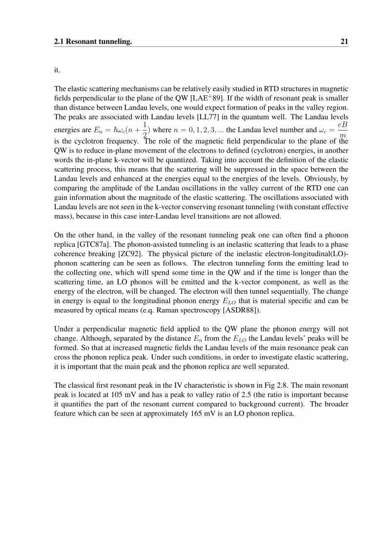
In-plane dispersion
Figure 2.10: Schematics of the broadening of the resonance. The interaction of the in-planedispersions of the emitter (black) and QW (grey) states represents the satisfaction of energy andmomentum conservation conditions. Notice that the Uinitial is much smaller than the Ubroadening.
2.2.2 Magnetic field in-plane of the QW.
Taking into account both energy and in-plane momentum conservation during tunneling intoa QW, a resonant peak in the I-V characteristic (at zero magnetic field) starts when a level inthe QW is aligned with Fermi energy in the injector. The resonant peak ends when this levelpasses the bottom of the conduction band in the injector (details in section 2.1.1). The effect ofa magnetic field perpendicular to the electron tunneling direction is to shift an electron k-vectorwhile tunneling (Lorentz force), so that it arrives in the quantum well with increased in-planemomentum. In this case, one needs to apply the energy conservation and “shifted” momentumconservation rule as depicted in Fig 2.10 and introduced by [ARM+90]. Uinitial is the Fermilevel in the injector and consequently the width of the resonance from the onset to maximum,Ubegin is a shift in the beginning of the resonance and Ubroadening is a new width of the resonance.Shift in the in-plane k-vector is
|∆kII | = eB∆z
~
As one can see Ubroadening > Uinitial means that the resonance is broadened in a traversal

2.2 Magnetic field influence on RTDs. 25
magnetic field. Moreover, the resonant is shifted to higher voltages (at the beginning of theresonance as well as at its maximum). The maximum of the resonant peak is not, in this case,the last energy at which the level in the QW overlaps with the levels in the injector (because themaximum overlap will occur before it).
Great experimental and theoretical attention was given to the problem of resonant tunneling un-der a transversal magnetic field. A quenching of the bistability in a bistable RTD with increasedin-plane magnetic field, that was observed experimentally [ZLT+90], can be used to investigateNDR region without use of NOR (see 3.2.3). At even higher magnetic fields, the broadeningdominates and the resonance is basically smeared out. Instead, formation of the magneticallyinduced oscillations is possible. These oscillations were explained in terms of the edge statesbound to the first barrier [HPE+89] and related to Landau levels’ quantization of the tunnelingelectrons. Theoretical investigation of coherent and sequential tunneling in double barriers withtransverse magnetic fields [PBT89] show that in some cases one can distinguish the level ofsequential tunneling from coherent with transverse magnetic field.
Very interesting experimental as well as theoretical investigation of RTD in a tilted magneticfield [GBGV91] evidently shows that in their RTD inter-Landau levels transitions are possiblein tilted magnetic field. Coherent transport model accounts for this affect and allows an ex-planation of the appearance of several satellites of the resonant current peak. Magnetic fielddependence is in good agreement with expected Landau levels spectra.
The big question about the in-plane magnetic field dependence of the phonon replica is not suf-ficiently addressed in literature. As it was shown in section 2.1.3, phonon-assisted tunneling isan inelastic scattering process which leads to the breaking of phase coherence. Inelastic scatter-ing means that the electron suffers energy loss as well as a change of wavevector. The energyloss is fixed by LO phonon energy, but the k-vector is partially randomised, still it is limited tothe allowed quantized values in the QW. Experimental observations of the transverse magneticfield dependence of the resonant peak and phonon replica [LKW+98] show quadratic shift inthe magnetic field of the resonant peak maximum and magnetic field independent position ofthe phonon replica.

26 Theory of Resonant tunneling.

Chapter 3
Experiment.
3.1 Diluted magnetic semiconductors.
3.1.1 Giant Zeeman splitting.
Paramagnetic DMS in a magnetic field has a spin splitting of the levels in the conduction andvalence band that is much larger than the value caused by the regular Zeeman term and is called“giant Zeeman splitting”.
The origin of the normal (regular) Zeeman effect is that in a magnetic field, the angular momen-tum quantum state can undergo a displacement from degeneracy, which can be understood clas-sically, as Lorentz predicted. For example, the p-orbital has three possible angular momentumquantum states that are degenerate (of the same energy) under normal circumstances. However,each angular momentum quantum state has a magnetic dipole moment associated with it, so theeffect of a magnetic field is to separate the three states into three different energy levels. Onestate increases in energy, one decreases in energy, and one remains at the same energy. Zeemandiscovered the effect, but under closer investigation it did not concur with Lorentz. The electronspin had not been discovered at the time of Zeeman’s original experiments, so the cases whereit contributed were considered anomalous. In fact, it was the anomalous Zeeman effect that ledto the discovery of spin.
In general, both orbital and spin moments are involved, and the Zeeman interaction takes theform
∆E =e
2m(−→L + 2
−→S ) · −→B = gLµBmjB (3.1)

28 Experiment.
where gL is the electron Lande g-factor and is one of the basic parameters in semiconductorsthat describes the magnitude of the Zeeman splitting of electronic states in magnetic fields. Theg-factor in semiconductors differs from the free electron g factor in vacuum, g=2.0023, due tothe spin-orbit interaction [RLZ59, BKR+03]. Depending on the semiconductor material, thisinteraction can change the effective g-factor by up to an order of magnitude and become positiveas well as negative. µB = e~
2me= 9.2740154 × 10⁻²⁴J/T = 5.788382 × 10⁻⁵eV/T is a Bohr
magneton. mj is a z-component of the total angular momentum. B is a magnetic field.
In the DMS materials a strong exchange interaction exist between the localised d-electrons ofmagnetic ions and the band electrons. When a magnetic field is applied the net alignment ofthe ions spin leads to the free carriers giant Zeeman energy splitting. This splitting is usuallymuch larger then the regular Zeeman one (Eq. 3.1) due to the direct action of magnetic field onelectron spin. In the case of giant Zeeman conduction band spin levels splitting ∆E of the DMSas a function of magnetic field B is given by a modified Brillouin function [GPF79]:
∆E = N0α x s0Bs (s g µBB/kB(T + Teff )) (3.2)
where N0α is the s-d exchange integral, x, s,and g are the manganese concentration, man-ganese spin, and g-factor respectively, and µB is the Bohr magneton. Bs is the Brillouinfunction of spin s. s0 and Teff are, respectively, the effective manganese spin and the ef-fective temperature. These phenomenological parameters are needed to account for antiferro-magnetic Mn++ −Mn++ exchange interactions [TvODP84, Fur88]. Functional dependenciesof these parameters on composition based on the data for Zn1−xMnxSe epilayers given bySeff = −0.804 + 0.364/(x− 0.109) and Teff = 47.2x− 281x2 + 714x3 [KYK+02].
Obviously, giant Zeeman splitting in low magnetic fields is stronger at lower temperatures. Theexplanation for this is that the material is in a paramagnetic state and the effect is a collectiveinfluence of oriented Mn++ atoms. Increased temperature disorients the manganese systemand in this way decreases the effect of the magnetic field. Therefore in order to reach the samegiant Zeeman splitting one has to apply higher magnetic fields. Simultaneously, decreasingtemperature below Teff does not make a great difference to the value of the splitting. Theconstant Teff term will dominate and the decreased temperature will not increase the value ofgiant Zeeman splitting in a constant magnetic field. This effect can be qualitatively understoodas an interaction between manganese atoms which dominates small temperature disorder at lowtemperatures.
The most pronounced influence of giant Zeeman splitting on properties of materials in magneticfield were observed in [Cd,Mn]Se, [Cd,Mn]Te, [Zn,Mn]Se, [Zn,Mn]Te [Sha86, SO87]. Wherethe effect of the density of states near Fermi energy produced large, but complicated magne-toresistance. Magnetic field induced change in the properties of the compound semiconductorscould be colossal if the carrier concentration was near to metal-insulator transition.

3.1 Diluted magnetic semiconductors. 29
a0
x [100]
y [010]
z [001]
0
XD
U
QL
Ã
L
S
S
ZWK
p4 /a
Figure 3.1: Zinc Blende crystal structure (left) with the first Brillouin zone for a fcc-Bravaislattice (right).
3.1.2 [Zn,Be,Mn]Se DMS.
The term “Diluted Magnetic Semiconductors” (DMS) was coined around 1980 [Gal79,PPV+82] and represents alloys of semiconductors and magnetic ions (transition metals or rareearths) which exhibit a variety of cooperative effects via spin exchange interactions [FK86].The exchange interaction between the conduction carriers and the localised moments of themagnetic ions can drastically alter the transport, optical, and magnetic properties of the hostsemiconductor. In general, DMS are based on II-VI and III-V semiconductors.
One of the most promising magnetic ions is manganese (Mn). The manganese Mn2+ has ahalf-filled d-shell that gives spin (5/2) per Mn atom. It does not produce carriers which areincorporated in II-VI semiconductors (isovalent) that allow control of the carriers type andconcentration independent of the Mn concentration.
Incorporation of the Mn ions in majority semiconductors is complicated by the fact that themanganese tends to segregate into separate phase, because of the fact that advanced growthmethods are required in order to receive good material quality.
ZnSe is a well-known semiconducting material with band gap of 2.8 eV. Optical propertiesattract most attention in this wide band gap semiconductor. On the other hand, the materialis known to have interesting electrical properties. It can be successfully doped by both n andp-type dopands, this is important for investigation of the fundamental transport properties ofsemiconducting structures. A crystal structure along with first Brillouin zone of ZnSe crystallattice is shown in Fig. 3.1. The lattice structure of the ZnSe crystal is a zinc-blende face-centredcubic (fcc) Bravais lattice. The high-symmetry lines are indicated in the figure in red colour.
Semiconductor alloy [Zn,Be]Se is very interesting from optical as well as transport and deviceengineering points of view. Beryllium incorporated in the ZnSe semiconductor replaces zinc

30 Experiment.
Figure 3.2: Energy-band structure of ZnSe and BeSe along with band gap evolution inZn1−xBexSe with Be content (from left to right after [CC76, Stu70, CTF00] accordingly).
and thus have little influence on the electronic structure of the material. Growth of the alloyis non-trivial and the advanced growth technique as molecular beam epitaxy (MBE) is used toproduce good quality of ternary alloy. Taking into account the Vegard’s law for compositiondependence of the lattice constant (approximately linear) and the fact that for ZnSe lattice con-stant is of 5.6676 A and for BeSe it is 5.139 A that means that the [Zn,Be]Se-ternary alloycan be grown lattice matched to GaAs substrates with only 3% Be content. The simplifiedapproximation for the lattice constants [Zn,Be]Se is
α0(Zn1−xBexSe) = −0.52x + 5.66
where x is the Be content 0 6 x 6 1.
Another important influence of Be on ZnSe crystal is to change the band gap. The picture isillustrated in Fig. 3.2. As one can see the ZnSe crystal has direct Γ − Γ and BeSe has indirectΓ − X band gap. Detailed evolution of the band gap with Be content is shown in the lastright inset of the figure. It can be seen that the composition dependence of the band gap is notlinear but rather has a bowing parameter. As it is shown in the [CTF00] the best fit for thelow-temperature, direct band gap of Zn1−xBexSe alloys is
EΓg (x) = 2.8(1− x) + 5.6x− 0.97x(1− x)
where x is the Be content and the bowing parameter is b = 0.97 eV.
In addition to the band gap change the band offset is changed with Be incorporation. Bandoffset for the conduction band is shown to be ∼ 60% of the band gap change [KKL+00]. Thismakes possible to design fairly complicated structures in a very flexible way. For example,the tunneling or resonant tunneling structure can be grown with parameters very close to wellknown [Al,Ga]As structures. One of the major advantages of this structure as compared with a

3.1 Diluted magnetic semiconductors. 31
0 1 2 3 4 5 60
4
8
12
16
201.3K_8%4K_8%8K_8%30K_8%
Zeem
an
split
ting,m
eV
Field, T
Figure 3.3: Left - magnetic phase diagram of Zn1−xMnxSe ternary DMS (after [LB87]).Right - temperature dependence of the magnetic field induced conduction band giant Zeemansplitting for the DMS with 8% Mn.
known one is that the indirect transition is much higher in energy.
The diluted magnetic semiconductor [Zn,Mn]Se is intensively used for investigation of fun-damental properties of semiconductors. It is II-VI binary compound in which a magnetic ion(M++) is substitutionally incorporated into the host crystal in the place of group-II element(Zn). Solid solution of Zn1−xMnxSe crystallise in the zinc-blende structure at x 6 0.30 andin wurtzite at 0.33 6 x. A reasonably good quality of the material can be grown by MBE withmanganese concentration up to 55 %.
The band gap of the ternary compound has highly nonlinear composition dependence. So,that at low Mn content the band gap is decreased, but after that it is bowed up and at lowtemperatures it comes back to its initial value at around 4 %. At higher contents the band gapis basically linearly increased [BBK+86]. Additionally, the return point when the band gap isequal to the initial one strongly depends on temperature. The return point happens at higher Mnconcentrations for higher temperatures.
Magnetic phase of the DMS is shown in Fig. 3.3 (left). At higher Mn concentrations the mag-netic phase is changed from paramagnetic to spin glass (see [LB87]).
The most exciting property of this material is the giant Zeeman splitting that in a mediate mag-netic field and at low temperatures is as great as 100 meV. 20 % of the total splitting corre-sponds to splitting of the conduction band. As it is explained in the previous section 3.1.1 thesplitting has nonlinear magnetic field dependence and saturates at high fields. The tempera-ture dependence of the magnetic field induced giant Zeeman conduction band splitting for theZn0.92Mn0.08Se DMS is shown in Fig. 3.3.
Such a large splitting of the conduction band in magnetic field is shown to give an extremely

32 Experiment.
high electron polarization∼ 100 % even at low fields [FKR+99]. In the same way as Y. Shapiraused density of states in CdMnSe conduction band to explain magnetoresistance data [Sha86]one could use the idea to explain the electron spin polarization. So, with an increased magneticfield the density of states for different spin species of electrons will be split in energy. It ispossible (in the case DOS has irregular shape) that the states for one spin specie will be out ofthe Fermi level range and the only allowed states for electrons will be spin-polarized.
The quaternary compound [Zn,Be,Mn]Se is a novel material system. It can be used to inves-tigate basic properties of semiconductors, electrical devices and spin transport. This tuneablecompound material is ideal for quantum devices design. In particular, in this system the bandgap, magnetic properties, as well as carriers concentration can be tuned independently. Incor-poration of [Be,Mn] in ZnSe does not introduce carriers and the material can be grown withsufficient quality using MBE.
3.2 Setup and sample design.
3.2.1 Measurement setup and technique.
I-V characteristics were measured on RTD structures in order to detect the effect of resonanttunneling. The measurements were done in a wide range of temperatures using low temperaturecryostats depending on the temperature range desired. The majority of measurements wereperformed in a 4He bath cryostat equipped with a needle valve between the main 4He bath anda sample space. A standard 8 T superconducting magnet is used to apply magnetic field to thesample. A 3He measurement cryostat equipped with 10 T superconducting magnet is used toreach temperatures in the range below 1 K and down to ∼ 300 mK. A 3He / 4He DilutionRefrigerator with 16 T magnet is used to measure samples at temperatures below 300 mK.
The samples are bonded (normally with an ultrasonic needle and a gold wire) to chip carriercontact pads. The 18 pins chip carrier is placed on a sample stick and inserted in the cryostat.Electrical contacts to the chip carrier are ensured by gold covered springs supporting highlyconductive needles. Resistance of the wires going down a cryostat is normally of the order of 3- 5 ohms.
In order to prevent the measurement circuit from going into oscillations (see section 3.2.3)a voltage stabilised power supply is connected to the sample in parallel with low impedanceparallel resistance [LAE+89] as in Fig 3.4. Current flowing through the device is calculatedfrom a voltage drop measured over the low impedance reference resistance. Ideally (to improvevoltage stabilisation) one does not use Rserial and keeps Rreference and Rparallel as small aspossible. Although, as we already know, these precautions are not always sufficient to removebistabilities, in our case, use of NOR is extremely difficult. At the same time, first resonancescould be easily stabilised with parallel resistor.

3.2 Setup and sample design. 33
Rserial sample Rreference
Rparallel
Vs Vr
VA
Figure 3.4: Circuit diagram for the measurement setup with a voltage divider Rserial−Rparallel
3.2.2 Charges in a RTD.
The charge distribution through an RTD structure has two characteristic features that play animportant role in the functionality of the device. The first one is the principle of resonant tun-neling based on charge accumulation in the QW. The accumulation is characterised by specificresonant state lifetime (2.10), broadening of the level (2.12) and the density of states (2.13).
Another, important charge accumulation region is placed in the injector of the device and attractswide attention [WCL+90, KJP+90, WLC+91, Pri92, HGPB95]. A simplified picture of an RTDwith the accumulation region is shown in Fig. 3.5(a). As one can see, quantization of the statesin the injector accumulation region is possible and in many cases the effect was used to improvepeak to value ratio. The basic idea behind it, is that the number of the resonant electrons atthe peak voltage will be increased by the presence of a quantized level. For the mechanismof the resonant tunneling one can expect a diode current due to scattering into the resonance-associated levels from the cathode side and out of them to the anode side, for correspondingrange of the external bias.
One of the successful approaches is the use of an emitter spacer layer as it is shown in Fig. 3.5(b)where the biased spacer layer is depicted in the inset. The influence of the spacer layer on peakto value ratio was shown experimentally by C. R. Wie and Y. W. Choi [WC91] and studiedtheoretically by the authors [CW92]. From these studies, it has been shown that the deeper theinjector spacer layer, the better the peak to value ratio. Obviously one has to take into account

34 Experiment.
L R
a) b)
Figure 3.5: The charge accumulation in RTD structures.
the possible formation of two-dimensional electron gas in the injector, which will drasticallyinfluence the magnetic field dependence of the device. Furthermore, the investigations done byC. R. Wie and Y. W. Choi were done with the layer depth within a first quasi-bound state in theaccumulation layer. With even deeper spacer layer, additional singularities in I-V characteristic(associated with higher quasi-bound states in the accumulation layer) can be seen.
Sequentially, presence of spacer layers in RTD was studied by using capacitance-voltage (C-V)measurements [WS94]. It is shown that the longer cathode spacer layer can result in a higherpeak in the C-V characteristic, while the anode space layer has a relatively small effect on thepeak and cut-off frequency.
3.2.3 Multistabilities in resonant tunneling structures.
A distinguishing feature of the I-V characteristic of an RTD is a negative differential resistanceNDR on the upper voltage slope of the resonant peak. Because of the presence of NDR thedevice in series with a resistance can go to oscillations between two or more steady states“bistability” [GTC87a] and produce high (terahertz) frequencies [SKW+94].
One has to distinguish the two major origins of the oscillations. The first comes from theresistance that is in series with the RTD and is within the measured voltage. Then the measuredvoltage will be the voltage drop on the device plus the voltage drop on the series resistance.Basically, the real I-V characteristic of the RTD will be shifted in bias by the voltage dropacross the series resistance. And, because the shift is proportional to the current, it is possiblethat the NDR region will not be reachable for standard constant voltage measurement setups.The situation is illustrated in Fig. 3.7(a) as compared to the original I-V curve shown in Fig. 2.8.One can see that even in the case of an ideal measurement setup in the NDR region there arefew steady states with different currents. In this case the system will be oscillating betweenthe states (A and B at applied VA) and within short voltage range and will go from one stateto another. The dashed area of the real I-V characteristic of the device will not be seen in theexperiment. It is possible to investigate such kinds of transition and see some part of the hidden

3.2 Setup and sample design. 35
I-V. For this one can sweep bias up and down and the “step” will happen at different voltagesthat will show a part of the I-V. In Fig. 3.7(a,b) the sweep directions are indicated by the arrows.
Another origin for such kind of bistability, which is also called as tristability [MLSE94] (be-cause there is an additional “hidden” steady state at the same voltages) could be an internalproperty of the device, known as an internal (bi, tri) multistability [GTC87a]. The internal mul-tistabilities are explained in terms of an electrostatic feedback due to charge build-up “chargeaccumulation” in the QW [LFM+96]. The idea is that the accumulated space-charge will mod-ify the electric field in the collector barrier. Taking into account the fact that the QW densityof states defining the charge accumulation is proportional to the broadening of the levels and
the state lifetime (see Eqs. (2.13) (2.12) (2.10)) that in the last case τ ≈ ~TmaxE0
where E0 is
a energy of the first level, the effect is bigger for wider barriers. In other words, the way tounderstand the intrinsic multistabilities is to treat the second (collector) barrier as a series resis-tance in the device that can bring the device to a multistable stage and is a necessary “intrinsic”device part (sequential tunneling picture). This simplified picture gives a good estimate for theorigin of the intrinsic multistabilities which make it easy to explain the increased influence ofthe effect in the asymmetrical structures.
In a real experimental environment the multistabilities can be caused by using a non-optimalmeasurements setup. If the series resistance is not taken into account, there are two cases.One where the series resistance is within the measured voltage. Then the influence of theresistance is the some as internal multistabilities depicted in Fig. 3.7(a). And, the second casewhere the series resistance is outside measured voltage. The load line method can then beused to determine the slope of the “step” in I-V as it is shown in Fig. 3.7(b). Assuming thereis a perfectly vertical load line (within value of the series resistance) the only difference involtage at different currents will be caused by a series resistance. Taking this into account onecan estimate a value of the series resistance in the measurement setup. For example for themeasurement shown in Fig. 3.7(c) the estimated series resistance (difference in voltage dividedby difference in current during the multistability step) is 82 Ohm.
The NDR region can be investigated using a voltage supply designed to have a load line withpositive slope as it is shown in Fig. 3.6 [LMS+94], equivalent to a voltage source and negativeseries resistance. This enables the portion of the I-V characteristic inside the region of apparentbistability to be examined. Such a device is an active circuit designed to have a negative outputresistance (NOR) [MLSE94] that compensate for the presence of the series resistance.
In the multistability regime the measurement setup goes into oscillations and, depending on thecapacitance and conductance of the measurement setup and RTD, the frequency will vary. Inthe standard DC measurement setup the oscillations will be averaged and the resulting shapeof the NDR region can have a complicated form as is seen in Fig. 3.7(d). Because of the highfrequencies produced by the device (up to several terahertz) use of the NOR in the RTD devicesis a complicated task and requires good technical and structural optimization.

36 Experiment.
I
VDR3
R2
R1Vin
+-
Figure 3.6: Circuit diagram for a NOR voltage supply. The output voltage is given byVD = Vin + (R1 •R3/R2)
0.00 0.05 0.10 0.15 0.20Voltage V,
Curr
ent,
Aµ
VA
A
B
0.00 0.05 0.10 0.15 0.200
10
20
30
40
Voltage V, VA
A
B
0.21
a) b)
0.0 0.1 0.2 0.3 0.4 0.50.0
0.2
0.4
0.6
0.8
1.0
UpDown
Curr
ent, m
A
Voltage, V
c)
0.0 0.1 0.2 0.3 0.4 0.50.0
0.2
0.4
0.6
0.8
1.0
Cu
rre
nt,
mA
Voltage, V
d)
Figure 3.7: I-V characteristic of an RTD with series resistance at multistabilities.

3.2 Setup and sample design. 37
GaAs Substrate
300nm Zn0.97Be0.03Se(8 )x1018
30nm ZnSe (1.5 )x1019
100nm ZnSe(1.5 )x10
19
Al/Ti/Au
GaAs Substrate
Ti/Au
10nm
Zn1-xMnxSe (i)
10nm ZnSe (i)10nm Zn0.97Be0.03Se (1018)
9nm
ZnSe (i)
5nm Zn0.7Be0.3Se (i)
15nm Zn0.97
Be0.03
Se (1018)
5nm Zn0. 7Be0. 3Se (i)
470 460 450 440 430 420 410 400 390
3.6
3.4
3.2
3.0
2.8
Ec
[arb
.units
]
distance [arb.units]
[Zn,Be,Mn]Se
Figure 3.8: Left - conduction band profile of the double barriers quantum well structure withinjector and collector regions. Right - layer structure of the device grown by MBE on GaAssubstrate.
3.2.4 Sample design.
The versatility of the [Zn,Be,Mn]Se material is used to investigate properties of magnetic semi-conductor structures. All-II-VI RTD structures from the material are grown by MBE.
One of the biggest concerns while designing the structure for MBE growth is the strain. Thatmeans that the lattice constant should not have rapid variation within the structure. Or, if this isthe case, the strained layer should be sufficiently thin. This makes the design of the structuressomewhat limited.
In Fig. 3.8 (left) the conduction band profile of the RTD is depicted. The dashed line in thefigure represents the Fermi level. The undoped [Zn,Mn]Se DMS quantum well is sandwichedbetween Zn.7Be.3Se tunnel barriers. The injector and collector regions consist of undopedZnSe separated from highly n-type doped ZnSe by low n-type doped [Zn,Be]Se with 3% Be.The idea behind the injector and collector step-like structure is to improve peak to value ratioas is discussed in the section 3.2.2.
The indirect (Γ - X or Γ - L) transitions in [Zn,Be]Se barriers are almost 1 eV higher than thedirect (Γ - Γ) transition (with 30% Be) as it is shown in Fig. 3.2. The electron effective mass inthe compound is the same as in the ZnSe semiconductor [Stu70] which avoids observation ofinter Landau levels mixing [ZTSS89, dSM88].
In Fig. 3.8 (right) the layer structure of the RTD is presented. The bottom (red) layer is a GaAssubstrate. After degassing the substrate, 300 mn of lattice matched Zn0.97Be0.03Se buffer isgrown by MBE. The buffer is doped until n = 8 ∗ 1018 cm−3. 100 nm of highly doped(n = 1.5 ∗ 1019 cm−3) ZnSe is grown over the buffer as a back side contacting layer. Thecollector region is formed by 10 nm of n = 1 ∗ 1018 cm−3 doped Zn0.97Be0.03Se and 10 nm

38 Experiment.
of intrinsic ZnSe. 5 nm thick Zn0.7Be0.3Se barriers are placed around 9 nm of intrinsic ZnSeQW. The injector region consists of 10 nm of intrinsic ZnSe and 15 nm of Zn0.97Be0.03Se withn = 1 ∗ 1018 cm−3 doping. 30 nm of highly n = 1.5 ∗ 1019 cm−3 doped ZnSe top contactlayer finalise MBE growth.
The top contacts are normally done by the deposition of a metal contact layer consisting of10 nm Al to achieve good contact, 10 nm Ti as a diffusion barrier, and 30 nm Au to avoidoxidation. To increase the quality of the contacts the samples are transferred from MBE tothe electron beam evaporation machine under ultra high vacuum conditions. This procedurereliably yields low contact resistivities of the order of 10−3 cm2. Heterostructures are patternedinto square mesas with sides of 100, 120, and 150 µm by optical lithography with positivephotoresist followed by metal evaporation and lift-off. Since the bottom contact can only befabricated after processing, it must rely on an ex situ technique where the contact resistivity istypically 1–3 orders of magnitude higher. Its resistance is kept reasonably low by a combinationof the incorporation of a highly n doped 100 nm ZnSe contact layer in the heterostructure, andthe use of a relatively large (5002 µm2) Ti-Au contact pad.
Chapter 4
Spin selection in RTDs with magnetic QW.
4.1 Introduction.
The physics governing spin injection and detection in semiconductor structures is now wellunderstood [SFM+00, Ras00, FJ01]. The problems associated with the impedance mismatchbetween a magnetic layer and the semiconductor can be overcome, e.g. by using dilute magneticsemiconductor injectors [FKR+99, OYB+99, SRG+01], or by fitting metallic magnetic contactswith tunnel barriers [MdBD+02] . However, these options can only be utilised to transfer ma-jority spin from the magnetic material into the non-magnetic layer and, similar to the situationin magnetic metallic multilayers, contacts with different shape anisotropy must be used whenthe direction of the spin of the electrons in the semiconductor is to be detected. Rather thanhaving to use an external magnetic field to switch the contact magnetisation, it would be verydesirable to have devices where the spin character of the injected or detected electrons could bevoltage selected. Here we report on the successful operation of a magnetic resonant tunnellingdiode (RTD), which we hope will prove useful for voltage controlled spin-polarized injectionand detection [DiV99].
The idea behind the RTD scheme is fairly straightforward but its realisation was previouslyhampered by material issues [GKF+01]. Since the well is made of a magnetic material, theenergy levels in the well will split into spin-up and spin-down states, as sketched in Fig. 4.1(b).By selectively bringing the spin-up or spin-down state into resonance, one can dramaticallyincrease the transmission probability of the desired spin species.
In this chapter, we describe our experimental investigations of an all-II-VI semiconductor RTDbased on ZnBeSe, and with a ZnMnSe dilute magnetic semiconductor (DMS) quantum well. Inthe presence of a (constant) magnetic field, the DMS exhibits a giant Zeeman splitting that, atlow temperatures, leads to an energy splitting of the Zeeman levels in the conduction band ofabout 15 meV at fields of one to two Tesla. Our samples show typical RTD-like current-voltage(I-V) characteristics with peak to valley ratios of over 2.5 to one. As a function of applied
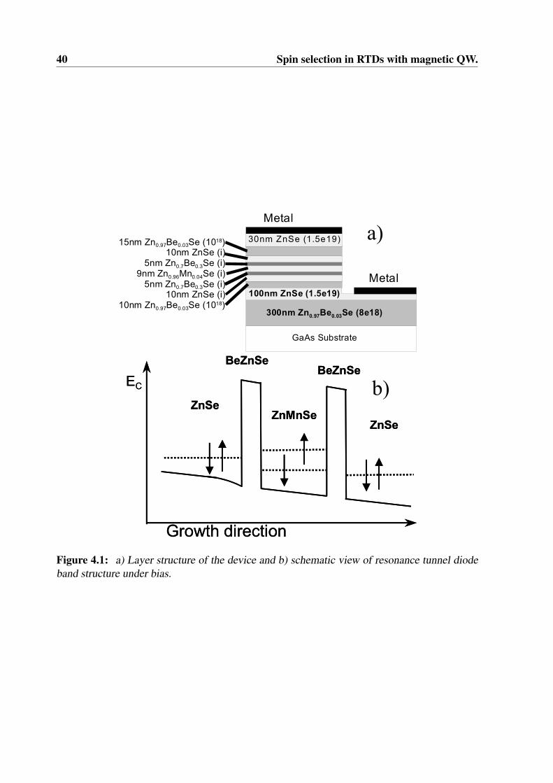
40 Spin selection in RTDs with magnetic QW.
GaAs Substrate
300nm Zn0.97Be0.03Se (8e18)
15nm Zn0.97Be0.03Se (1018)10nm ZnSe (i)
5nm Zn0.7Be0.3Se (i)9nm Zn0.96Mn0.04Se (i)
5nm Zn0.7Be0.3Se (i)10nm ZnSe (i)
10nm Zn0.97Be0.03Se (1018)
30nm ZnSe (1.5e19)
100nm ZnSe (1.5e19)
Metal
Metal
a)
b)EC
BeZnSe
Growth direction
ZnMnSeZnSe
ZnSe
BeZnSeEC
BeZnSe
Growth direction
ZnMnSeZnSe
ZnSe
BeZnSe
Figure 4.1: a) Layer structure of the device and b) schematic view of resonance tunnel diodeband structure under bias.

4.2 Details of the experiment. 41
magnetic field, the transmission resonance of the I-V curve splits into two peaks with a splittingcorresponding to the separation of the energy levels in the well.
4.2 Details of the experiment.
The investigated II-VI semiconductor heterostructures were grown by molecular-beam epitaxyon insulating GaAs substrates. The active region of the device consists of a 9 nm thick undopedZn.96Mn.04Se quantum well, sandwiched between two 5 nm thick undoped Zn.7Be.3Se barriers.The complete layer structure is shown in Fig. 4.1 along with a schematic of the potential energyprofile of the double-barrier structure under bias. The bottom 300 nm of Zn.97Be.03Se, highlyn-type doped with iodine to a concentration of n=8*1018cm−3, as well as the 15 and 10 nm thickZn.97Be.03Se layers with n=1*1018 cm−3 in the injector and collector contain 3% Be in orderto be lattice matched to the GaAs substrate. The barrier layers are clearly not lattice matchedto the substrate, but are sufficiently thin to be grown as fully strained epitaxial layers. Theheterostructure was patterned into square mesas with side of 100, 120 and 150 µm by opticallithography with positive photoresist followed by metal evaporation and lift off.
Special care must be taken in order to obtain good ohmic contact to the II-VI semiconductor.For the top contact, this can be achieved by in-situ growth of a metal contact layer consistingof 10 nm Al to achieve good contact, 10 nm Ti as a diffusion barrier, and 30 nm Au to avoidoxidation. This procedure reliably yields contact resistivities of the order of 10−3Ω.cm2. Sincethe bottom contact can only be fabricated after processing, it must rely on an ex-situ techniquewhere the contact resistivity is typically 1-3 orders of magnitude higher. Its resistance is keptreasonably low by a combination of the incorporation of a highly n doped 100 nm ZnSe contactlayer in the heterostructure, and the use of a relatively large (5002µm2) Ti-Au contact pad.
The samples were inserted into a 4He bath cryostat equipped with a 6 T superconducting mag-net, and were investigated using standard low noise electrical characterization techniques. Pre-cautions were taken to prevent problems associated with the measurement circuit going intooscillations. A stabilised voltage source was used to apply bias to the circuit, which consistsof the RTD, a 33 Ohm reference resistance in series and a 40 Ohm resistor in parallel. Such asetup is known to prevent bi-stability of the circuit in the region of negative differential resis-tance [LAE+89]. By measuring the voltage drop over the RTD and the reference resistor as thebias voltage is swept, I-V curves of the RTD can be extracted. The absence of charging in thedevice was confirmed by comparing I-V curves with a different sweep direction [MLSE94].
We studied devices with Mn concentrations of 4% and 8% in the quantum well layer. Thelayers’ thicknesses of the 4% sample are given in Fig. 4.1, whereas those for the 8% Mn sampleare all 6% thinner. For structures with 4% Mn in the well, the first resonance for positive biasoccurs at 105 mV and has a peak to valley ratio of 2.5 whereas for the 8% Mn sample theresonance is at 127 mV with a peak to valley ratio 2.25. The size of the mesas had no effect onthe position and strength of the resonance.

42 Spin selection in RTDs with magnetic QW.
4.3 Results and simulation of spin resolved current throughthe device.
I-V characteristics of the RTDs were measured in different magnetic fields in a range from 0to 6T applied either perpendicularly to or in the plane of the quantum well. The results forperpendicular magnetic fields are presented in Fig. 4.2 (lines). For clarity, subsequent curvesare offset by 10 µA. It is clear from the figure that the resonance is split into two parts andthat the splitting grows as a function of the magnetic field. At 6 T, the separation between themaxima of the split peaks is 36.5 mV and 42 mV for 4% and 8% Mn samples respectively. Thebroader feature which can be seen most prominently in the zero field curve at approximately165 mV (180 mV) for the 4% (8%) of Mn samples is an LO phonon replica [LAE+89].
To explain the magnetic field-induced behaviour of the resonance, we develop a model basedon the Giant Zeeman splitting for the spin levels in the DMS quantum well. First, we extractthe series contact resistance of the RTD from the measured I-V curve at zero magnetic field[MLSE94, LMS+94]. Then we assume that each of the two spin split levels have the sameconductance, and therefore that each carries half of the current in the device.
We neglect the slight relative change of barrier height caused by the change in energy of the lev-els, and assume that the conductivity of each level is independent of magnetic field in the sensethat for the same alignment between the emitter Fermi level and the well level, the conductivitywill be the same. In other words, the conductivity of each level as a function of applied voltagein the presence of a magnetic field can be given by a simple translation of the zero field curveby a voltage corresponding to the energy shift of the pertinent spin level in the well.
After translation, we add the conductivity contributions of both the spin-up and the spin-downcurves, and reinsert the series resistance to yield a modelled I-V curve at a given magnetic field.By comparing this I-V curve with the actual experimental curve at 6 T, we determine an optimalvalue of 330 Ohm (900 Ohm) for the series resistance for the 8% (4%) Mn sample. Using thisvalue of the series resistance for all modelled curves, and fitting the modelled curves at eachfield to the experimental ones, we extract the voltage splitting of the levels ∆V as a function ofthe magnetic field. Fig. 4.2 shows the modelled I-V curves as the circles, which compare verywell with the experimental data presented as the solid lines in the figure.
We now compare the values of ∆V extracted from this fitting procedure to the expected behav-iour of the spin levels in the wells. The spin level splitting ∆E of the DMS as a function ofmagnetic field B is given by a modified Brillouin function [GPF79]:
∆E = N0α x s0Bs (s g µBB/kB(T + Teff )) ,
where N0α is the s-d exchange integral, x, s, and g are the manganese concentration, manganesespin, and g-factor respectively, and µB is the Bohr magneton. Bs is the Brillouin function of

4.3 Results and simulation of spin resolved current through the device. 43
0.00 0.05 0.10 0.15 0.200
25
50
75
100
125
150
6T
3T
0T
8% Mn
T=1.3K
Voltage (V)
Cu
rrent
(µA
)
0.00 0.05 0.10 0.15 0.200
25
50
75
100
125
6T
3T
0T
4% Mn
T=1.3K
Voltage (V)
Cu
rre
nt
(µA
)
a)
b)
Figure 4.2: Experimental (lines) and modelled (circles) I-V curves for a resonance tunneldiode with a) Zn.92Mn.08Se and b) Zn.96Mn.04Se in the quantum well. Curves taken in 0.5Tintervals from 0 to 3T and in 1T intervals from 3T to 6T.

44 Spin selection in RTDs with magnetic QW.
spin s. s0 and Teff are, respectively, the effective manganese spin and the effective tempera-ture. These phenomenological parameters are needed to account for Mn interactions. Takingestablished values of Teff = 2.24 K, s0 = 1.13 [YTFP95] for x=8% (Teff= 1.44 K, s0 = 1.64 forx = 4%) and N0α 0.26 eV [TvODP84] from the literature, we obtain values for ∆E which areplotted as the solid lines in Fig. 4.3(a) for temperatures of 1.3, 4.2, and 8K and for Mn concen-trations of 4% and 8%. These curves are compared with the values of ∆E extracted from theexperiment (symbols in the same figure) for measurements taken at the respective temperatures.It is important to note that in order to correctly fit the amplitude to the Brillouin function, themeasured values of ∆V must be divided by a lever arm of 2.1. The agreement between themagnetic field dependence of the experimental values and the Brillouin function is remarkable,suggesting that our model of two spin level splitting in a magnetic field captures the essentialcharacter of the device. More over an identical value of the lever arm is found for both the 4%and 8% Mn samples.
The existence of a lever factor between the experimental voltage splitting and the theoreticalenergy splitting in the well is a well-known feature of RTDs. It occurs because only part of thevoltage applied to the device is dropped over the first barrier, and thus effective in determiningthe alignment condition for the resonance. Furthermore, extracting the lever factor for our diodeby comparing the observed voltage splitting in the B = 0 I-V curve between the first resonanceand the phonon replica to the known LO phonon energy of ZnSe (31.7 meV) [LB87] also yieldsa lever arm of around 2.
In Fig. 4.3(b) we compare measurements at 3T with magnetic field in the plane of, and perpen-dicular to the quantum well. The curves are offset for clarity. Evidently, the peaks in the I-Vcurve for in-plane magnetic fields are broader than those for perpendicular fields and are shiftedslightly towards higher bias voltages. This effect is known from GaAs based RTDs [AMR+88]and can be explained in terms of momentum conservation. For magnetic field in-plane (per-pendicular to the motion of the electrons) the Lorentz force will give the electrons an in-planemomentum. The conservation of in-plane momentum during the tunnelling process forces elec-trons to tunnel into finite momentum states of the quantum well, which are at a higher energythan the zero momentum ground state. Furthermore, the spread in in-plane k vectors leads toa broadening of the tunnelling resonance [AMR+88, DNPK87]. From the figure, it is obviousthat the splitting of the resonance peak is similar in both orientations of magnetic field. This isdue to the isotropic g-factor in the DMS. This observation directly rules out any explanation ofthe peak structure as resulting from Landau level splitting in the quantum well.
Temperature dependent measurements of the 6T I-V curves are presented in Fig. 4.4, again withthe curves offset for clarity. Qualitatively, an increase in temperature has a similar effect on theI-V curves as a reduction of the magnetic field (cf. Equ. 1). The peaks move closer togetherand eventually merge back into a single peak. On the other hand, the zero field I-V curves arepractically temperature independent in the range from 1.3 Kelvin to 30 Kelvin. The reductionof the splitting as a function of field can be anticipated from the results of Fig. 4.3, and is simplya manifestation of the temperature dependence of the giant Zeeman splitting of the DMS. Thissuggests that any operational limit imposed on the device by temperature is purely a function ofthe material in the well, and that no inherent limit from the tunnelling process is detected.

4.3 Results and simulation of spin resolved current through the device. 45
0.00 0.05 0.10 0.15 0.200
20
40
60
II
L
8% Mn
T=1.3K_3T
Voltage, V
Cu
rre
nt,
µA
0 1 2 3 4 5 60
4
8
12
16
20 1.3K_8%
4.2K_8%
8K_8%
1.3K_4%
4K_4%
8K_4%
Ze
em
an s
plit
ting
(m
eV
)
Field (T)
a)
b)
Figure 4.3: a) Giant Zeeman splitting versus magnetic field for both samples. The lines comefrom a Brillouin-like description of the well levels. The symbols represent the splitting in thepeak positions extracted from the experimental data. b) I-V curves for sample with 8% Mn,under 3T in-plane (II) or perpendicular (L) magnetic field.

46 Spin selection in RTDs with magnetic QW.
0.00 0.05 0.10 0.15 0.20
0
20
40
60
80
100
30K
8K
4.2K
1.3K
8% Mn
B=6T
Voltage (V)
Curr
ent
(µA
)
0.00 0.05 0.10 0.15 0.20
0
20
40
60
80
30K
8K
4.2K
1.3K
4% Mn
B=6T
Voltage (V)
Curr
en
t (µ
A)
a)
b)
Figure 4.4: Temperature dependence of the I-V curves of the first resonance, shown for eachof the diodes.

4.4 Summary. 47
4.4 Summary.
To summarise, we have presented results of all II-VI semiconductor RTDs based on the(Zn,Be)Se system, with magnetic impurities (Mn) in the quantum well. A strong splitting ofquantum well resonance is observed as a function of magnetic field, which originates from theGiant Zeeman splitting of the spin levels in the dilute magnetic semiconductor quantum well.An intuitive model that simulates the magnetic field dependence of the I-V characteristic of thedevice is discussed, and shows positive agreement with the experiment. The results thereforedemonstrate the possibility of devices based on tunnelling through spin resolved energy lev-els. Experiments aiming to measure the spin polarization of the current flowing through such adevice are currently underway.

48 Spin selection in RTDs with magnetic QW.

Chapter 5
RTD with magnetic QW as a spin detector.
5.1 Spin polarization at high magnetic field.
As was already mentioned in the section 3.1.2, because of giant Zeeman splitting, a high spinpolarization of the electron current (up to 100%) can be achieved in [Zn,Mn]Se DMS in inter-mediate magnetic fields [FKR+99]. Similarly, regular Zeeman splitting can, at high magneticfields, lead to a spin-polarized current in the injector. Regular Zeeman splitting has a linearmagnetic field dependence, and for ZnSe can be as big as 1.1 meV at 14 Tesla.
The conduction band profile for the RTD at high magnetic fields is shown in Fig. 5.1 with indi-cation of the regular Zeeman splitting of the conduction band levels in the injector. The splittingis present throughout the entire device, but the injector spin polarization is most important forour experiment. Even though the Fermi energy in the injector is much larger than the regularZeeman splitting, taking into account the conduction band profile, one can expect the incomingcurrent to be spin-polarized. The spin polarization will change the electro-chemical potentialin the injector and influence the resonance peaks. In the case of a nonmagnetic RTD, the spinpolarization in the injector will be partially compensated. As the electro-chemical potential forone spin species decreases with increased spin polarization, the other will also increase.
In our case of giant Zeeman split levels in the QW, we expect current spin polarization in theinjector to decrease the amplitude of the minority peak and increase that of the majority one.The majority current spin polarization is generated by the lower (in energy) regular Zeeman splitstates of the conduction band of the injector. The regular Zeeman splitting in ZnSe has the samesign as the giant Zeeman term for the [Zn,Mn]Se conduction band. This means that the majoritycurrent spin polarization corresponds to the lower giant Zeeman split level in the QW. The peakat higher bias (minority spin polarization) will thus decrease when the spin polarization of thecurrent in the injector is increased. The effect of the current spin polarization is mainly observedat high magnetic fields because the regular Zeeman splitting at intermediate fields is relativelysmall compared to the estimated Fermi energy.

50 RTD with magnetic QW as a spin detector.
470 460 450 440 430 420 410 400 390
3.8
3.6
3.4
3.2
3.0
2.8
Ec
[arb
.units
]
distance [arb.units]
Figure 5.1: At very high magnetic fields, the regular Zeeman splitting in the nonmagnetic ZnSeinjector spin polarizes the incoming current.
5.2 Influence of spin-polarized current on RTDs I-V charac-teristics.
The high magnetic field and low temperatures I-V dependence were measured in the 16 T 4Hebath cryostat and at Dilution Refrigerator.
In Fig. 5.2, I-V curves at 0 (red), 6 (blue) and 14 (magenta) T are shown. In the range ofmagnetic fields from 0 to 6 T the only major effect to be seen is the splitting of the levels in theQW that force the resonance peak to split in voltage. At magnetic fields higher than 6 T, thegiant Zeeman splitting is basically saturated and does not have a strong influence on the positionor the shape of the resonances with a greater increase in B. On the other hand, a very strongeffect is still observable at magnetic fields above 6 T. The high voltage resonance decreases inamplitude and the low voltage one increases. This dependence is expected for spin-polarizedcurrent in the injector (see section 5.1).
The magnetic field dependence of the I-V characteristic for the sample with 8% Mn in the QWat 1 K is shown in Fig. 5.2 (left). The curves are offset by 25 µA for clarity. At the same timeas the low voltage resonance increases in amplitude at high magnetic fields, the higher voltageresonance “practically“ vanishes by 14 T.
I-V curves are shown in Fig. 5.2 (right) for the 4% Mn in the QW sample at 1.3 K. With thecurves are offset by 15 µA. The effect of spin-polarized current on this RTD I-V curve is not

5.2 Influence of spin-polarized current on RTDs I-V characteristics. 51
0.00 0.05 0.10 0.15 0.200
25
50
75
100
125
0T
6T
14T
8% MnT=1K
Voltage (V)
Curr
ent(µ
A)
0.00 0.05 0.10 0.15 0.200
20
40
60
0T
6T
14T
4% MnT=1.3K
Voltage (V)
Curr
ent(µ
A)
Figure 5.2: I-V characteristics at high magnetic field are compared with 6 and 0 T curves. Left- the curves are shown for the sample with 8% Mn in the QW. Right - for the 4% Mn sample.In the range of magnetic fields from 6 to 14 T (when the giant Zeeman splitting is basicallysaturated) spin polarization of the current in the injector gradually suppresses the higher energyresonance and enhances the lower energy one.
as big as for the sample with 8% Mn. On the other hand, the fact that both spin peaks and theirphonon replicas are well pronounced at 14 T is obvious proof of the spin polarization in theinjector changing the peak ratio.
In order to take into account orbital effects in a magnetic field perpendicular to the QW, verydetailed (second derivative) analyses were performed. The negative of the second derivativeplot is useful to analyse the position of the peaks because the peaks preserve their positions.Moreover, the appearance of the peaks is significantly magnified and even inflaction on an I-Vcurve can become a full peak with a region of negative slope. For this reason, it is hard tointerpret the shape of the resonance but the position of the maximum can be analysed.
In Fig. 5.3 the second derivative of the I-V characteristics of the 4% Mn sample are shown forperpendicular magnetic field ranging from 0 to 14 T in half Tesla steps. The measurementsare done at 1.3 K and the curves are offset for clarity. Each resonance and its phonon replicapair at 14 T are identified by a number (1 or 2). The red line indicates a first Landau levelquantized sub-peak in the phonon replica of the first resonance peak. In the presence of aperpendicular magnetic field, landau level quantization within the phonon replica is expected[LAE+89] (see section 2.1.3). The voltage separation between the phonon replica peak and theLandau level at 14 T is indicated by the green arrow and corresponds to the expected energiesof the first Landau level with a leverage factor near 2.1 (similar to the results obtained fromthe giant Zeeman splitting of the levels in the QW). No additional peaks were found in theI-V characteristics, even in the second derivative plot, indicating that the elastic scattering isreasonably low in our samples.
The in-plane high magnetic field dependence of the I-V characteristic for the sample with 4%Mn in the QW at 1.3 K is shown in Fig. 5.4. The curves are measured every half Tesla and offsetfor clarity. The giant Zeeman split resonant peak seen up to 5 Tesla seem to be gone on the 14 T

52 RTD with magnetic QW as a spin detector.
0.05 0.10 0.15 0.20
-0.2
0.0
0.2
0.4
0.6
0.8
1.0
1.2
14T
0T4%Mn
-d2I/dV
2
Voltage, (V)
1 2hù
C
Figure 5.3: Negative of second derivative of the current versus voltage at 1.3 K measured inthe perpendicular magnetic fields from 0 to 14 Tesla (see Fig. 5.2 right). The black line showsthe phonon replica of the first resonance and the red line shows first Landau level.

5.3 Temperature dependence of the effect. 53
0.00 0.05 0.10 0.15 0.200
20
40
60
80
100
120
14T
0T
4%MnT=1.3K
Curr
ent,
(µA
)
Voltage, (V)
Figure 5.4: In-plane to the QW magnetic field dependence of the I-V curve at high magneticfields.
curve. As was shown in section 2.2.2 under in-plane magnetic field the k-vector conservationand Lorentz force smooth the resonance peak and the extreme case of this effect is seen in thefigure.
The second derivative analysis of the 14 T in-plane magnetic field I-V curve for the 4% Mnsample is show in Fig. 5.5. As one can see, the resonances are well detectable even though theyare not obvious in the I-V curve. Each resonance peak and its phonon replica pairs are indicatedby a number (1 or 2). Additionally, the second LO phonon resonance of the first resonance isindicated by 1’. It results from tunneling electrons getting into the QW resonance level energiesafter losing the energy of LO phonon twice.
5.3 Temperature dependence of the effect.
For [Zn,Mn]Se with 8% Mn, the Mn concentration dependent effective temperature (Teff ) inthe equation for the giant Zeeman splitting Eq. 3.2 has a value of 2.24 K [TvODP84]. Reducingthe temperature to much lower than Teff should not have a great effect on the value of giantZeeman splitting, especially at high magnetic fields. On the other hand, from the phase diagramof the DMS ternary compound Fig. 3.3 (left) one can guess that at low temperatures a magneticphase transition from paramagnetic to spin glass magnetic state can happen.
In Fig. 5.6, 40 mK I-V curves are shown in the magnetic field range from 0 to 16 T with 2 T

54 RTD with magnetic QW as a spin detector.
0.00 0.05 0.10 0.15 0.20
-0.03
-0.02
-0.01
0.00
0.01
1.3K_14TIn plane
4%Mn
-d2I/dV
2
Voltage, (V)
1 21’
Figure 5.5: Reversed second derivative of the current versus voltage at 1.3 K measured in thein-plane magnetic field 14 Tesla (see Fig. 5.4). By 1’ the second phonon replica of the firstresonance is shown.
steps. The curves are offset for clarity. The limiting factor for the temperature was a currentheating the sample but not the Dilution Refrigerator which has a base temperature of 5 mK.From the data, it is possible to conclude that the giant Zeeman splitting did indeed not changemuch in the temperature range between 1 K and 40 mK. Moreover, the fact that the splittingcorresponds to the value expected for the giant Zeeman splitting in the paramagnetic [Zn,Mn]Sesuggests that no magnetic phase transition took place at these temperatures.
In Fig. 5.7 (left), the regular Zeeman splitting dependence of the I-V characteristic of the RTDat various temperatures with a magnetic field chosen to keep giant Zeeman splitting (shown bydEGzeeman) constant, is presented. Under these conditions, one can see that at higher tempera-tures the spin resolved peak ratio is changed. The reason for this happening is simple. The giantZeeman splitting has a strong temperature dependence and thus the magnetic field needed toreach the chosen value of dEGzeeman at higher temperatures is much greater than at lower tem-peratures. The regular Zeeman splitting, however, is temperature independent and has a linearmagnetic field dependence. At higher temperatures, and accordingly at higher magnetic fields,the regular Zeeman splitting in the injector polarizes the current and the peak ratio changes.When the temperature is decreased, a lower magnetic field is needed to preserve the value ofthe giant Zeeman splitting and the smaller value of the regular Zeeman splitting is not sufficientto polarize the current in the injector as efficiently. This is why the peak ratio returns to the val-ues expected for a non polarized injector electrons. The temperatures at which the I-V curveswere measured are shown in the legend on the left side, whereas the right side legend gives thecorresponding values of the regular Zeeman splitting in the injector.

5.3 Temperature dependence of the effect. 55
0.00 0.05 0.10 0.15 0.20 0.250
25
50
75
100
125
150
6T
16T
0T
8% MnT=40mK
Voltage (V)
Curr
ent(µ
A)
Figure 5.6: Very low temperature (40 mK) I-V curves measured to high magnetic fields show-ing no magnetic phase transition in the 8% Mn DMS at this temperature.
0.00 0.05 0.10 0.15 0.200
5
10
15
20
25
30
35
0.97meV0.83meV0.68meV0.54meV0.38meV0.2meV
12K10K8K6K4K1.3K
4%MndEGzeeman=14.88meV
Curr
ent,
(µA
)
Voltage, (V)0.00 0.05 0.10 0.15 0.200
10
20
30
40
50
0.1meV0.52meV0.86meV1.3meV
1.2K6K10K15K
8%MnB=16TdE
zeeman=1.1meV
Curr
ent,
(µA
)
Voltage, (V)
Figure 5.7: Left - the regular Zeeman splitting dependence of the I-V characteristic of the RTDat different temperatures with magnetic field chosen to keep giant Zeeman splitting (shown bydEGzeeman) constant. The temperatures are shown in the legend on the left and correspondingvalues of regular Zeeman splitting are shown in the legend on the right. Right - temperaturedependence of the I-V curve at 16 Tesla (constant regular Zeeman splitting shown as dEzeeman).In the right legend kT calculated from the temperatures in the left legend are shown.

56 RTD with magnetic QW as a spin detector.
In Fig. 5.7 (right), the temperature dependence of the effect of the spin polarization in the in-jector is shown. The I-V characteristics measured at different temperatures and constant (high)16 T magnetic field. The regular Zeeman splitting (dEzeeman) at the magnetic field is 1.1 meV .In this temperature range the giant Zeeman splitting has a weak temperature dependence. Thetemperatures at which the I-V curves were measured are shown on the left side and the corre-sponding values of kT are shown in the legend on the right. At higher temperatures the peakratio changes its value to that observed at lower magnetic fields ≤ 6 T. This is caused by thetemperature-induced decrease in spin polarization of the current in the injector. By comparingthe values of the regular Zeeman spin splitting of the conduction band in the injector with thevalue of temperature broadening described by kT, one can already see at 12 K that kT is biggerthan the Zeeman splitting, causing the reduced spin polarization seen in our measurement.

Chapter 6
Double RTD with magnetic QWs forcurrent spin polarization and detection.
In Fig. 6.1, a schematic diagram of a non-local measurement scheme for a double RTD structureis shown. The RTDs are biased independently and connected (within spin flip length of eachother) in the collector contact. Current spin polarization created by one of the RTDs influencespotential drop over the other. The spin dependant difference in potential drop over the structureis caused by the difference in electro-chemical potential of spin polarized collector electrons.This can be understood in analogy to band bending in the injector when charge accumulationchanges the band profile. If the sign of collector spin polarization matches the spin polarizationof the resonance peak, the peak position is shifted to a lower bias at increased spin polariza-tion. This shift is proportional to the increased electro-chemical potential for the correspondingspin orientation. Correspondingly, the electro-chemical potential for minority spin-polarizedelectrons decreases, and the spin resonant peak shifts to higher bias at higher spin polarization.
A simulation procedure similar to the one used for the magnetic field dependence of the RTD
+ +
R
µ
µ
Figure 6.1: Schematic diagram of the double RTD with magnetic QW structure in magneticfield under bias.

58 Double RTD with magnetic QWs for current spin polarization and detection.
0
10
20
30
40
50
60
60 80 100 120 140 160 180Detector v , mVolage
V_injector=84mVV_injector=112mVV_injector=126mVD
ete
cto
r curr
ent, µ
A
Figure 6.2: I-V characteristics of the detector RTD as a function of the bias over the injectorRTD.
with magnetic QW (see section 4.3) is applied to predict the collector spin polarization de-pendence of the RTD I-V characteristic in constant magnetic field. The spin polarization isrecalculated from the I-V curve of the simulated RTD with magnetic QW.
Fig. 6.2 presents results of a calculation of the detector RTD I-V characteristics in a magneticfield and with the incoming current polarized by a similar RTD structure. To simplify thediscussion, one of the structures will be called the simulated RTD ”detector” and the RTDproducing the spin polarization ”injector”. In a real structure the devices will have a symmetricinfluence on each other and the problem should be solved self-consistently, but our simplifiedapproach illustrates the ideas.
Depending on the voltage drop on the injector RTD, the collector current spin polarization ofthe detector RTD will correspond to the lower or higher energy resonant peak. In the case ofspin polarization of the same sign as the lower energy peak, the first peak will shift to lowerbias and the higher energy peak will shift to a higher bias. The separation between the peakswill thus increase. This situation is shown in Fig. 6.2 by the red curve. When the collectorspin polarization corresponds to the spin polarization of the higher resonance, the separationbetween the peaks will decrease as shown by the blue curve in the figure. An intermediate statewith lower spin polarization is shown by the green curve.
A three dimensional representation of the injector RTD voltage drop influence on the I-V char-acteristic of the detector RTD is shown in Fig. 6.3. The peaks move apart when the spin polar-ization corresponds to the lower resonance in the injector RTD and becomes closer when thespin polarization is the same sign as the higher resonance. The peaks move to the expectedvalues when the spin polarization decreases.

59
Figure 6.3: Colour plot of the detector RTD current as a function of the bias over the injectorand the detector RTDs.

60 Double RTD with magnetic QWs for current spin polarization and detection.
Figure 6.4: Colour plot of the measured detector RTD current as a function of the bias overthe injector and the detector RTDs.
Fig. 6.4 presents preliminary results of measurements on a double RTD structure operated inthe configuration sketched in Fig. 6.1, done by A. Groger. The RTDs with [Zn,Mn]Se QW werepatterned in two 800 nm square mesas separated by a distance of 200 nm and measured at 4 Kand 6 T. The white lines are guides to the eye indicating the resonance peaks corresponding toone of the RTDs. The arrows show the crossing points of the resonance peaks of the injector andcollector RTDs. The crossing points are separated differently, depending on the resonance withwhich the crossing is happening. The result could be interpreted as an effect of the collectorspin polarization.

Chapter 7
RTD with magnetic injector or barriersfor spin manipulation.
7.1 Introduction and the magnetic injector sample design.
Some interesting designs for eventual spintronics devices are structures based on magnetic semi-conductor resonant tunneling diodes (RTDs) which have promising futures as spin filters andspin aligners. However, before these structures can make their way into actual devices, we mustfirst understand the basic behaviours of these magnetic structures and how they differ from theirnon-magnetic counterparts. We have previously explored the behaviour of RTDs with a mag-netic quantum well [SGS+03] and now turn our attention to RTDs fitted with magnetic injectors.Here, the polarization of spin originates in the bulk behaviour of the injector, and the RTD itselfis ostensively a non-magnetic device which is fed with a polarized source of electrons. As amagnetic field increases, we observe important changes in the transport characteristics of theRTD stemming from the realignment of the band profile in the device, and explain how this canbe understood in the framework of a Landauer-Buttiker–type model. The correct understand-ing of this mechanism is therefore essential before proceeding to more sophisticated devicestructures combining spin injection, detection and manipulation.
The studied sample is an all II-VI semiconductor resonant tunneling diode structure with aconduction band profile similar to that used in previous work on II-VI and III-V [SGS+03] andfitted with a dilute magnetic semiconductor (DMS) injector layer. The tunneling region consistsof a 9 nm thick ZnSe quantum well (QW) sandwiched between two 5 nm thick Zn.7Be.3Sebarriers. Below the tunneling region is a 10 nm thick ZnSe collector layer. The injector is a10 nm thick Zn.94Mn.06Se layer which is used to inject spin polarized electrons into the diode.The remaining layers are needed to ensure a proper doping profile and to allow for the fitting ofhigh quality ohmic contacts. Full details of the layer stack are given in Fig. 7.1(a).

62 RTD with magnetic injector or barriers for spin manipulation.
a)
GaAs Substrate
300nm Zn0.97Be0.03Se(8 )x1018
30nm ZnSe (1.5 )x1019
100nm ZnSe
(1.5 )x1019
Al/Ti/Au
GaAs Substrate
Ti/Au
10nm Zn0.94
Mn0.06
Se (i)
10nm ZnSe (i)
10nm Zn0.97
Be0.03
Se (1018)
9nm ZnSe (i)
5nm Zn0.7
Be0.3
Se (i)
15nm Zn0.97
Be0.03
Se (1018)
5nm Zn0.7
Be0.3
Se (i)
b)
ZnMnSe
ZnSe
ZnSe
ZnBeSe
ZnBeSe
Ec
Gro
ws
dir
ecti
on
Figure 7.1: a) Layer structure of the device and b) schematic view of resonance tunnel diodeband structure under an applied bias.
The contact resistance of the devices is kept to a minimum by using an in-situ Al(10 nm)/Ti(10 nm)/Au (30 nm) top contact, while the ex-situ bottom contact is fabricated by etching downto the very highly doped ZnSe layer, and using large area (5002µm2) Ti-Au contact pad. Thesample is patterned in 100 µm2 pillars using standard optical lithography, which wet each andlift-off.
Measurements are performed in 4He bath cryostat equipped with a high field superconductingmagnet using standard DC transport techniques. Care was taken to construct a circuit with alow (40 Ω) resistor in parallel to the diode to prevent the diode from going into oscillationsin the negative differential conductance region [LAE+89]. Current measurements consist ofmeasuring the voltage drop across a relatively small 30 Ohm series resistor.
A schematic of the band profile is shown in Fig. 7.1. Both the injector and collector sides ofthe tunneling structure are gradient doped in order to insure a relatively low Fermi energy atthe point of injection, and thus a sharp resonance [WC91]. Under the influence of an externalmagnetic field, the DMS injector exhibits giant Zeeman splitting of up to 20 mV in the conduc-tion band, and the degeneracy of its spin states is lifted following a Brillouin function [GPF79],creating a spin-polarized carrier population via the transfer of electrons from the higher energyspin band to the lower one. In order to maintain proper alignment of the Fermi energy, thisimbalance in the population of the two spin species must lead to a splitting of the bottom of thespin up and spin down conduction bands, leading to different band profiles for each of the spinspecies in the injector region, as indicated in the diagram.

7.2 Magnetic field induced change of I-V characteristic of RTD structure with magneticinjector. 63
0 25 50 75 100 125 1500
5
10
15
20
10T
0TCurr
ent,
µA
Voltage, mV
Figure 7.2: Magnetic field dependence of the I-V curves of the first resonance at 4.2 K.
7.2 Magnetic field induced change of I-V characteristic ofRTD structure with magnetic injector.
Current-voltage characteristics for the device for different amplitudes of perpendicular-to-planemagnetic fields (B) are shown in Fig. 7.2. At zero field, the sample has typical RTD behaviour,showing a strong resonance peak at 36 mV with a peak to valley ration of just over 1. Theadditional resonance visible at 96 mV in the B = 0 curve is the well known LO phonon replica[LAE+89], which is separated from the direct resonance by the energy of the LO phonon ofthe well material, and can be used to calibrate the voltage scale to energy levels in the QW. Aresonance associated with the second well level occurs at around 0.3 V (not shown in the figure).As is often the case, the resonances for the negative bias direction are not as pronounced. Weconfirmed the absence of charging effects in the device by verifying that I-V curves for differentsweep directions were identical [MLSE94].
As a magnetic field is applied, the peak shifts to higher voltages and strongly increases inamplitude. The strongest dependence of the peak amplitude and position on the magnetic fieldis observed at low fields, with the behaviour saturating before 10 T. The behaviour is thereforeconsistent with the Brillouin like behaviour expected from the giant Zeeman splitting of theinjector. Note also that the phonon replica causes a higher energy echo of the QW state, butsince the effects we are studying result from properties of the injector, the phonon replica peaksimply follows the magnetic field dependence of the main resonance.

64 RTD with magnetic injector or barriers for spin manipulation.
0 20 40 60 80 1000
2
4
6
8
10
12
14
0T
8K4 K.2
1.3KC
urr
ent,
µA
Voltage, mV
Figure 7.3: Temperature dependence of the resonance.
Figure 7.3 shows the temperature dependence of the 2 T I-V curve for temperatures from 1.3to 8 K. The B = 0 curve, which is temperature independent in this range, is included forcomparison. It is clear that the increase in temperature has a similar effect on the I-V curves asa lowering in the magnetic field would. Indeed, we verified that the only effect of temperatureis to rescale the effect of the magnetic field on the Zeeman splitting in the injector, exactly aswould be expected from the argument of the Brillouin function that scales as B/(T + Teff) asdescribed below.
7.3 Explanation of magnetic field influence on the transportin RTD with magnetic injector.
The slight shift of the peak to a higher bias with increasing magnetic field is fairly intuitive andcan be directly expected from the schematic of Fig. 7.1. It is well established that the maximumof resonance occurs when the bottom of the conduction band is brought into alignment withthe well level[Lur85]. As the field increases, the peak becomes evermore dominated by themajority spin conduction band. Since the bottom of this band is moving to lower energies, ahigher bias will be required to bring this band into alignment with the well level, producing ashift of resonance towards a higher bias.
The large increase in the current amplitude is also related to the change of the conduction

7.3 Explanation of magnetic field influence on the transport in RTD with magneticinjector. 65
band energy with magnetic field B, but its manifestation is somewhat more subtle. Let Eσ =Ec+sh/2 denote the spin-split band bottom with h as the spin splitting [s = +(−) for σ =↑(↓)].Due to the exchange interaction between localised Mn ions and band electrons there arises inthe DMS a giant Zeeman splitting,
h = N0αxS0BS[SgµBB/kB(T + Teff)] , (7.1)
where N0α is the exchange integral, x the Mn concentration of S = 5/2 Mn spins, g is the Landefactor, Bs the Brillouin function, and S0 and Teff are the Mn effective spin and temperature,respectively. One might naively expect that a spin splitting of the conduction band leaves theDMS injector electron density constant (keeping EF fixed). This is indeed correct for a 2Dinjector [SMP02] since the spin-dependent density nσ = (m/2π~2)(EF − Eσ) is independentof the energy because the density of states is constant. However, for a 3D system nσ dependsnonlinearly on h, thereby the total electron density n = n↑ + n↓ is shown to be an increasingfunction of h provided EF remains fixed. Since the current peak is mainly determined by n, itfollows from Eq. 7.1 that the peak amplitude increases with B. Therefore, the current increaseeffect has a geometrical origin.
To gain further insight, we perform numerical simulations of the electron transport along thez-direction [growth direction, see Fig. 7.1(b)]. Because a similar peak amplitude increase isalso observed when B is an in-plane magnetic field indicating that the effect is independent ofthe direction of the magnetic field, orbital effects are not taken into account. In addition, weneglect spin relaxation effects and the current density J = J↑ + J↓ is thus carried by both spinspecies in parallel,
Jσ =em
4π2~3
∞∫
eV +sh/2
dEzdE⊥ Tσ(Ez, ε0, V ) (7.2)
× [fL(Ez + E⊥)− fR(Ez + E⊥)] ,
with V the bias voltage applied to the structure. We take into account the spin splitting in thelongitudinal energy Ez. The Fermi functions fL and fR describe the distribution of electronswith total energy Ez + E⊥ in the left and right leads with electrochemical potentials µL = EF
and µL = EF − eV , respectively. Band-edge effects are incorporated in the lower limit of theintegral.
In Eq. 7.2, the transmission T conserves the momentum parallel to the interfaces and depends,quite generally, on Ez, V and the subband bottom energy ε0 of the quantum well. Close toresonance, it is a good approach to take a Lorentzian shape, Tσ = ΓL
σΓRσ /[(Ez − ε0)
2 + Γ2/4],where ΓL
σ (ΓRσ ) is the partial decay width due to coupling to the lead L (R) and Γ = ΓL + ΓR
the total broadening per spin. We hereinafter consider symmetric barriers for simplicity but it

66 RTD with magnetic injector or barriers for spin manipulation.
0 25 50 75 100 125 150Voltage (mV)
0
3
6
9
12
15
Cur
rent
(µA
)
0 1 2h/E
F
0
1
[Jp(h
)-J p(0
)]/J
p(0) Experiment
Theory Γ(E)Theory Γ=const
Figure 7.4: Theoretical I–V curves at 4 K for an RTD with a spin-polarized injector increasingthe spin splitting from h = 0 to h = 2EF in steps of h = 0.2EF (from bottom to top). Inset:normalized current peak Jp as a function of h. Experimental and model data are shown forcomparison.
is important in the strongly nonlinear regime (i.e. around the current peak) to take into accountthe energy (and voltage) dependence of the tunneling rates[BB99]. The barrier height is givenby the conduction band offset between ZnSe and Zn0.7Be0.3Se, which is approximately 0.6 eV.Using ZnSe parameters we find for the first resonant level ε0 = 21 meV. Now spin saturationtakes place at around h = 20 meV, thereby EF = 10 meV. This implies that for small resonancewidth the onset of the I–V curves of Fig. 7.2 should occur at ε0 − EF = 11 meV. This fact,together with the low peak-to-valley ratio that the I–V curves exhibit, suggests a large value ofΓ, probably due to disorder or interface roughness. Therefore, we set Γ = 15 meV at V = 0and h = 0 and fit the peak current at B = 0 with the experimental value.
We show the results in Fig. 7.4 from h = 0 to h = 2EF . The I-V curves reproduce the exper-imental observations and the agreement is fairly good. The negative differential conductanceregion extends all the way from the resonance peak because we consider only the first resonantlevel. We note that in Fig. 7.4 the voltage axis is scaled with a lever arm L = 2, consistedwith that extracted from the position of the phonon replica. Since the broadening is a largeenergy scale, we can expand Eq. 7.2 at zero temperature in powers of 1/Γ. We find for smallspin splittings that the resonance peaks at eVres/L = ε0 − EF /3 + h2/3EF . Substituting theparameters, we obtain Vres = 37 mV at h = 0, in accordance with Fig. 7.2. Moreover, thisexpression clearly shows the shift of Vres with increasing h. Inserting this result into Eq. 7.2 wefind to the leading order of 1/Γ that the current peak Jp = (em/2π2~3)E2
F (1 + h2/4E2F ) is in-
deed an increasing function of the magnetic field. In the inset of Fig. 7.4 we present the currentpeak as a function of h, showing a remarkable agreement with the experimental observations.

7.4 RTD with magnetic barriers for spin manipulation. 67
In comparison, we provide the current increase when the energy dependence of Γ is neglected,which qualitatively agrees with our results, indicating that the simple model (7.2) captures thekey points of the experiment.
The results we obtain are reminiscent of Ref. [CW92], where the In content of a GaInAs emitterin a III-V RTD is varied. As a consequence, the band alignment changes and the peak currentincreases. In our case, the increase is due exclusively to the giant spin splitting in the injector.Thus, the current increase can be tuned with a magnetic field without changing the sampleparameters.
In conclusion, we have presented I-V characteristics of a II-VI resonant-tunneling diode at-tached to a diluted magnetic semiconductor injector. We have observed both an enhancementand a voltage shift of the resonance current peak when the applied magnetic field increases. Theresults are consistent with a giant Zeeman splitting in the injector since the current saturates at afew Tesla and the temperature dependence follows the magnetisation of a paramagnetic system.The Zeeman splitting induced redistribution of spin carriers in the injector leads to a modifi-cation of the conduction band structure of the device which is responsible for the changes intransport properties. We have discussed a transport model which replicates most of the fea-tures seen in the experiment. Our findings offer the unique possibility of producing high peakcurrents which arise from spin effects only.
7.4 RTD with magnetic barriers for spin manipulation.
An interesting sample design with diluted magnetic material in the barriers of the RTD devicemight also be expected to trigger a rise in spin selection in the structure. In a magnetic fieldthe height of the barriers will be modified for each spin orientation. Taking into account thattunneling probability has as exponential dependence on the barrier height, even a small changein the barriers could drastically change the I-V characteristic.
The schematic conduction band profile for a sample with 6% Mn [Zn,Mn]Se DMS barriersunder a bias and an external magnetic field is shown in Fig. 7.5 (left). The green lines indicatethe splitting of the top of the barriers. In Fig. 7.5 (right) the sample layer structure as it is grownby MBE is depicted.
A 0 T and 4 K I-V characteristic is shown in Fig. 7.6. At positive bias the first resonance witha peak to valley ratio of 2.4 is seen at 69 mV and its phonon replica at around 135 mV . Thestructure is quite asymmetric and we will concentrate on the current direction with the mostpronounced resonance peak.
Perpendicular to the plane of the QW magnetic field dependence of the I-V peak at 4 K is shownin Fig. 7.7 (left). The magnetic field is swept from 0 to 13 T in 1 T steps. The dependence isrelatively small for such a large magnetic field range. The size of the effect can be understood

68 RTD with magnetic injector or barriers for spin manipulation.
GaAs Substrate
300nm Zn0.97Be0.03Se(8 )x1018
30nm ZnSe (1.5 )x1019
100nm ZnSe(1.5 )x10
19
Al/Ti/Au
GaAs Substrate
Ti/Au
10nm
ZnSe (i)
10nm ZnSe (i)10nm Zn0.97Be0.03Se (1018)
9nm5nm
15nm Zn0.97
Be0.03
Se (1018)
5nm Zn0. 64Be0. 3 Se (i)
470 460 450 440 430 420 410 400 390
3.8
3.6
3.4
3.2
3.0
2.8
[Zn,Be,Mn]Se
Ec
[arb
.units
]
distance [arb.units]
0.06Mn
Zn0. 64Be0. 3 Se (i)0.06
Mn
ZnSe (i)
Figure 7.5: Right - schematic conduction band profile under bias and magnetic field. Left -the sample layer profile.
0 50 100 150 2000
100
200
3006% MnT=4K; B=0
Voltage (mV)
Curr
ent(µ
A)
Figure 7.6: 0 T and 4 K I-V characteristic of the resonant tunneling structure with 6% Mn inboth barriers.

7.4 RTD with magnetic barriers for spin manipulation. 69
0 50 100 150 2000
50
100
150
200
250
300
B=13T
B=0T
6% MnT=4K
Curr
ent(µ
A)
Voltage (mV)0 50 100 150 200
0
50
100
150
200
250
300B=13T
B=0T
6% MnT=4K
Curr
ent(µ
A)
Voltage (mV)
Figure 7.7: Left - perpendicular to the QW plane magnetic field dependence of the I-V char-acteristic for the sample with 6% Mn in the barriers. Right - in-plane of the QW magnetic fieldmeasurements for the same sample.
taking into account the facts that the giant Zeeman splitting is small compared to the barriers,which are around ∼ 250 meV high, and the resonance peak is formed “basically“ at the bottomof the barriers. Moreover, in addition to the effect being small, its magnetic field behaviour isopposite to the one observed in the cases of the magnetic injector or quantum well. Namely,the magnetic field induced increase in the resonance current does not saturate, but instead thedistance between I-V characteristics is increased at higher fields. Again, such dependence canbe understood by assuming that the lower giant Zeeman split barrier starts to dominate theprocess exponentially. Under these conditions even a small change in the splitting at higherfields will produce great change in the I-V characteristic. This means that we could have muchstronger spin polarization effects than seen on I-V, especially at high fields.
In Fig. 7.7 (right) an in-plane magnetic field measurement of the structure is presented. Theeffect is a manifestation of the Lorentz force modified k-vector of the tunneling electrons (seesection 2.2.2).

70 RTD with magnetic injector or barriers for spin manipulation.

Chapter 8
Spin resolved resonant tunneling inself-assembled quantum dots.
8.1 Self-Assembled II-V Quantum Dot as a Voltage-Controlled Spin-Filter.
Nanomagnetics has produced a series of fascinating and often unanticipated phenomena overthe past few years. To name a few, molecular magnets exhibit quantum tunneling of the magneti-sation [TLB+96], magnetic atoms on a surface exhibit giant magnetic anisotropies [GRV+03],and magnetic domain walls are being harnessed as data carriers [RBG+03]. Here, we reporton another remarkable phenomenon: self-assembled quantum dots, fabricated from II-VI DMSthat macroscopically exhibit paramagnetism, possess a remnant magnetisation at zero externalfield. This allows us to operate the dots as voltage controlled spin filters, capable of spin-selective carrier injection and detection in semiconductors. Such spin filter devices could pro-vide a key element in the emergence of a full spintronics technology [WAB+01, Aws02, Ohn02].We present the first experimental observation of such a device using an approach based onthe incorporation of non-magnetic CdSe self-assembled quantum dots (SADs) in paramagnetic[Zn,Be,Mn]Se (see section 3.1.2).
We previously demonstrated a prototype of such a spin filter using a II-VI DMS-based resonanttunnelling diode [SGS+03]. However, while that device was tuned by a bias voltage, the spinfiltering mechanism still requires an external magnetic field. Moreover, ferromagnetic III-Vsemiconductors like [Ga,Mn]As are not suitable for resonant tunneling devices due to the shortmean free path of holes [MGJ+03]. Recent theoretical works [HGQ91, ERR01, FRB04] havesuggested that spin selection may be achievable in II-VI DMS without any external magneticfield by creating localised carriers that might mediate a local ferromagnetic interaction betweennearby Mn atoms.

72 Spin resolved resonant tunneling in self-assembled quantum dots.
GaAs Substrate
300nm Zn0.97Be0.03Se(8e18)
10nm ZnSe (i)
10nm ZnSe (i)
30nm ZnSe (1.5e19)
100nm ZnSe (1.5e19)
Al/Ti/Au
Ti/Au
15nm Zn0.97Be0.03Se (1018)
10nm Zn0.97Be0.03Se (1018)
1 3ML QD. CdSe (i)
5nm Zn0.64Be0.3Mn0.06Se (i)
5nm Zn0.64Be0.3Mn0.06Se (i)
GaAs Substrate
300nm Zn0.97Be0.03Se(8 10 )x18
10nm ZnSe (i)
10nm ZnSe (i)
30nm ZnSe (1.5 10 )x19
100nm ZnSe (1.5 10 )x19
Al/Ti/Au
Ti/Au
15nm Zn0.97Be0.03Se (1018)
10nm Zn0.97Be0.03Se (1018)
CdSe (i)
5nm Zn0.64Be0.3Mn0.06Se (i)
5nm Zn0.64Be0.3Mn0.06Se (i)
Figure 8.1: Full layer structure of the device and schematic of the transport mechanism. Aselectrons tunnel through the quantum dot, they mediate a local magnetic interaction betweennearby Mn ions causing them to align ferromagnetically.
8.2 Sample and measurements details.
Our sample is an MBE-grown all-II-VI RTD structure consisting of a single 9 nmthick semi-magnetic Zn0.64Be0.3Mn0.06Se tunnel barrier, sandwiched between gradient dopedZn0.97Be0.03Se injector and collector. Embedded within the barrier are 1.3 monolayers of CdSe.The lattice mismatch between the CdSe and the Zn0.64Be0.3Mn0.06Se induces a strain in theCdSe material, which is relaxed by the formation of isolated CdSe dots [MTB+01]. The fulllayer stack is given in Fig. 8.1. Standard optical lithography techniques were used to patternthe structure into 100 µm square pillars and contacts were applied to the top and bottom ZnSelayers in order to perform transport measurements vertically through the layer stack. More de-tails of the fabrication procedure are given in section 3.2.1. From the size of the pillars, andthe typical density of the dots, one would expect some million dots within our device. How-ever, despite this number, transport through similar III-V SAD-RTDs is usually dominated byonly a few dots that come into resonance at lower bias voltages [HPM+01, VLP+00, TIM+98].We, therefore, interpret the low bias transport through our sample as corresponding to electronstunneling from the injector into a single quantum dot and out of the dot into the collector asschematically depicted in Fig. 8.1. Based on calculations of energy levels of strained quan-tum dots, we find several quantum dot levels populated by electrons at zero bias. Hence, theelectrons tunnel through excited states of quantum dots containing a finite number of electrons.

8.3 Magnetic field evolution of the resonance peaks. 73
0 20 40 60 80 100 120 140 1600.0
0.5
1.0
1.5
2.0
2.5
3.0
T=4KB=0T
Curr
ent,
nA
Voltage, mV
45 50 55 60 65
40
50
60
70
80
4T
0T
Curr
ent,
pA
Voltage, mV
Figure 8.2: Current-voltage characteristic of the device, with a high-resolution view of thefirst resonance feature in the inset, clearly showing a strong magnetic field dependence of theresonances.
The experiments were carried out in a magnetocryostat and studied at temperatures as low as1.3 K and in fields from 0 to 6 T. Fig. 8.2 shows a full current voltage curve up to a biasvoltage of 170 mV. The first feature is observed at a bias of 55 mV, associated with the firstdot coming into resonance. At a bias voltage above 100 mV, several resonances, due to theensemble of dots, can also be observed. We will first focus on the low bias feature which isshown in the inset to the figure. These more detailed curves taken at 0 and 4 T clearly showthat the feature actually has a complex structure, consisting of four distinct peaks, which evolvewith the magnitude of the applied magnetic field. We verified that the evolution of the featuresdoes not appreciably depend on the direction of the magnetic field, indicating that the magneticresponse of the system cannot be associated with artefacts such as two-dimensional states in theinjector or wetting layer [SGS+03, HPM+01, VLP+00, TIM+98] and it must be a property ofthe dot or the barrier. We also verified that the sample does not exhibit any magnetic hysteresis.
8.3 Magnetic field evolution of the resonance peaks.
A better understanding of the evolution of the features with magnetic field can be obtained fromFig. 8.3. In Fig. 8.3(left), we plot the current through the device as a colour-scale surface withrespect to a bias voltage and magnetic field. This proves two very important features of the data.Firstly, that as the magnetic field is increased, features split apart with a behaviour reminiscent

74 Spin resolved resonant tunneling in self-assembled quantum dots.
Figure 8.3: On the left - a surface plot of the current through the device as a function of amagnetic field and bias voltage in the region of the first resonance feature. On the right - acolour-scale image of the resonances as a function of a magnetic field and voltage for higherbias resonances. Since these higher resonances are weaker and on a significant background, thecolour-scale on the right part is proportional to the voltage derivative of the current in order tobetter resolve the position of the resonances. In both cases, the data at higher magnetic fieldsclearly has Brillouin-like behaviour, as proved in the right figure, where Brillouin functions areplotted as lines. However, at fields below ∼ 500 mT, the behaviour departs from a Brillouinfunction, with the splitting becoming constant and remaining finite even at zero magnetic field.
of the Brillouin function, and secondly, that the splitting remains finite in zero external magneticfield. The same behaviour can be seen for many of the higher bias resonances presented inFig. 8.3(right). The first of these effects, that the levels should split following a Brillouinfunction, is not very surprising. It was previously observed in III-V devices that resonancessplit in a magnetic field following the Lande g factor of the material in the dots [TIM+98].
The main difference here is that in the present experiment it is the barrier, and not the dots,that are magnetic. Since the effect of the giant Zeeman splitting on the height of the barriersis negligible, the presence of Mn should have little effect on the barrier properties. However,given that electrons are not perfectly localised in the dots, but rather have wave functions whichextend into the barrier, it is not surprising that the quantum levels in the dots spin-split followingthe magnetisation of the Mn in the barriers, yielding results reminiscent of those previouslyobserved [SGS+03] in the case of tunneling through a dilute magnetic quantum well.
The observation that the splitting remains finite at B = 0 T is however more surprising sincethere is a priori nothing ferromagnetic in the sample. This observation can be understood byconsidering the effect of interactions between electrons in the dot and the Mn atoms in thevicinity of the dot.
8.4 Understanding the effect of an external magnetic field. 75
8.4 Understanding the effect of an external magnetic field.
Electrons populate quantum dot levels according to the Pauli exclusion principle, and Hundsrules [HK03] whenever there is orbital degeneracy. For a parabolic dot, the total electron spinfollows the sequence S = 1/2,0,1/2,1,1/2,0,1/2,1,3/2,. . . with increasing electron numbers.Hence, for almost all electron numbers, the total spin of the dot is finite. The interaction of thistotal net spin with the spin of Mn ions induces an effective ferromagnetic Mn-Mn interaction.This can be seen by considering the total Hamiltonian of the electronic and Mn system [HGQ91,ERR01, BlG97, HME+00]:
H = He + g∗µB~B ·
∑i
~Si − JC
∑
~R,i
~MR·~Siδ(~ri − ~R)
+∑
~R
gMnµB~B · ~M~R +
1
2
∑
~R,~R′
J~R,~R′~M~R· ~M~R′
Here ~M~R is the spin of Mn ions (M=5/2) at position ~R, Si is the spin of the i-th electron(S=1/2). Jc is the sp-d exchange constant between the conduction electrons and the d-electronsof the Mn shell and JRR′ is the anti-ferromagnetic Mn-Mn interaction. The first term is thespin independent Hamiltonian of electrons confined to a quantum dot in a magnetic field, andinteracting via a pair-wise potential. The full interaction between electron spins and Mn ionsin the barrier is an extremely complicated issue. We restrict ourselves here to a demonstrationthat the electron spin is capable of compensating the anti-ferromagnetic interaction among Mnions and lead to their ferromagnetic arrangement. We consider only a single electron in theground state and in the absence of external magnetic field, leaving the problem of interactingmany-electron dots for future analyses. The effective spin Hamiltonian now reads:
H = E0 − JC
∑
~R
|Φ(R)|2 ~MR·~S +1
2
∑
~R,~R′
J~R,~R′~M~R· ~M~R′ (8.1)
where E0 is the electron energy and |Φ(R)|2 is the probability of finding an electron at theposition ~R of a Mn ion. Even for such a simplified Hamiltonian the number of configura-tions is very large in the number of Mn ions. The physics of Mn-Mn interactions mediatedby electron spin can however be understood by examining an exactly solvable problem of twoanti-ferromagnetically coupled Mn ions. The energy spectrum of the coupled Mn-spin systemis characterised by the total spin J=M±1/2 where M is the total Mn spin and the ±1/2 cor-responds to the direction of the electron spin. The evolution of the energy of the system as afunction of the total Mn spin depends on the direction of the electron spin in the following way:

76 Spin resolved resonant tunneling in self-assembled quantum dots.
E(M, +) = −(JC
2)M + (
JNN ′
2)[M(M + 1)− 35
2]
E(M,−) = (JC
2)(M + 1) + (
JNN ′
2)[M(M + 1)− 35
2]
as shown in Fig. 8.4(left). In the absence of coupling to the electron spin (Jc = 0), it is obviousthat the minimum energy state for either electron spin corresponds to the total Mn spin M=0,i.e. an antiferromagnetic arrangement. However, as shown in Fig. 8.4(left), with couplingto the electron spin, the E(M, +) ground state of the combined system has a finite total Mnspin M∗ = ( JC
JNN′− 1)/2. To estimate the value of M∗ we approximate our quantum dot by a
spherical CdSe dot with radius R= 4 nm and a barrier potential of 1 eV estimated from strain andthe Bir-Pikus Hamiltonian. The effective electron-Mn exchange interaction for Mn ions on thesurface of the sphere is then given by JC = JC |Φ(R)|2 = 4.5 µeV. For a typical Mn separation inthe barrier of R12 = 1.2 nm, we estimate the antiferromagnetic interaction strength J12 = 1 µeV.Hence for our model system we find M∗ = 2 and the coupling to electron spin aligns spinsof nearest neighbouring Mn ions. Independent mean field calculations involving tens of Mnions randomly distributed in the barrier around a spherical or disk shaped quantum dots confirmthe existence of ferromagnetic ordering of Mn ions in the vicinity of quantum dots [FRB04].In Fig. 8.4(right), we show the calculated averaged Mn and electron spin magnetisation asa function of temperature for Mn ions localised in the barrier surrounding a spherical CdSequantum dot with radius of 4 nm and Mn concentration of 4%. We find the existence of themagnetic polaron, with the Mn magnetisation decaying as one moves away from the quantumdot. These finding are in agreement with previous calculations of magnetic polarons [HGQ91,ERR01, FRB04], and for reasonable parameters for our system shows that the presence ofelectrons in the dot will mediate a local ferromagnetic interaction between Mn atoms near thisdot.
The interpretation of our experimental observations is therefore clear. Electrons localised inthe dot mediate a local ferromagnetic interaction which causes a finite spin splitting even inthe absence of an external applied field. Our experiment is therefore tantamount to measuringtransport through a single magnetic polaron. The local interaction has a strength correspondingto an effective field of the order of some hundreds of mT, and can be randomly oriented. Whenan external magnetic field is then applied, the ferromagnetic order will first rotate towards thedirection of the applied field, but this will have no effect on the transport, which explains why inthe experimental data, the resonance positions are independent of the magnetic field for fieldsbelow ∼ 500 mT. However, as the magnetic field is further increased, it will start to dominateand the spin splitting will grow following the normal paramagnetic interaction of the dilute Mnsystem [SGS+03]. A question remains as to why the zero magnetic field splitting is observedhere while it was not seen in the optical measurements of Ref. [HME+00, MGN+04]. Thishowever can be understood by the fact that once current begins flowing through the dot, afeedback mechanism sets in where spin polarization of the current enhances the polarizationof Mn spins which in turn enhances the polarization of the current [HGQ91, ERR01]. This

8.4 Understanding the effect of an external magnetic field. 77
0 1 2 3 4 5
-10-8-6-4-202468
E(M,-)
E(M,+) M*
JC=4.5 meV,
J12
=1 meV
Energ
y(µ
eV
)
M0 10 20 30 40 50 60 70 80
0.0
0.2
0.4
0.6
0.8
1.0
1.2
1.4
1.6
<M><S>
<M
>(<
S>)
N=12, JNN'
=1.0 meV,
x=0.04,R=40 Å, L=1 Å
T (mK)
Figure 8.4: On the left - the energy levels E[+,M], E[-,M] for two different electron spinorientations as a function of total spin of two Mn ions M localised on a surface of sphericalquantum dot and on the right - average magnetisation as a function of temperature of Mn ionsrandomly distributed on a surface of spherical quantum dot.
dynamical effect also explains why spin polarization is observed at much a higher temperaturethan the predicted temperature dependence of magneto-polaron of Fig. 8.4(right).
In conclusion, we have shown that electrons in a quantum dot can mediate a local ferromag-netic interaction in a surrounding dilute Mn system and that this leads to a finite energy splittingof spin levels in the dot in the absence of an external magnetic field. Coupled with the reso-nant tunneling scheme which allows the bias controlled selection of which dot level is usedin tunneling, our results open up exciting new possibilities of a voltage controlled spin filter,which can operate in the absence of any external magnetic field, without relying on an inherentferromagnetism of the component materials.

78 Spin resolved resonant tunneling in self-assembled quantum dots.

Summary
Spintronics is a rapidly growing field in physics and presently attracts much attention. Spin-tronics aims to exploit the spin properties of the electron instead of, or in addition to, chargedegrees of freedom, for the development of a novel generation of devices.
In this work we investigate magnetic resonant tunneling diode (RTD) structures for spin manip-ulation. All-II-VI semiconductor RTD structures based on [Zn,Be]Se are grown by MBE. Weobserve a strong, magnetic field induced, splitting of the resonance peaks in the I-V character-istics of RTDs with [Zn,Mn]Se diluted magnetic semiconductors (DMS) quantum well (QW).The splitting saturates at high fields and has strong temperature dependence. A phonon replicaof the resonance is also observed and has similar behaviour to the peak.
We develop a model based on the giant Zeeman splitting of the spin levels in the DMS quantumwell in order to explain the magnetic field induced behaviour of the resonance. First, we extractthe series contact resistance of the RTD from the measured I-V curve at zero magnetic field[MLSE94, LMS+94]. Then we assume that each of the two spin split levels have the same con-ductance and that each, therefore, carries half of the current in the device. We also assume thatthe conductivity of each level as a function of applied voltage, and in the presence of a magneticfield can be given by a simple translation of the zero field curve by a voltage corresponding tothe energy shift of the pertinent spin level in the well. After translation, we add the conductivitycontributions of both the spin-up and spin-down channels, and reinsert the series resistance.By comparing this modelled I-V curve with the experimental curve we are able to determinethe optimal value of series’ resistance and the voltage splitting of the levels. The modelledI-V curves compare very well with the experimental data. Moreover, the series resistance ismagnetic field independent. We find a remarkable agreement between the magnetic field de-pendence of the experimental values and the modified Brillouin function [GPF79] describinggiant Zeeman splitting. The agreement is valid at all temperatures and Mn concentrations. Inorder to correctly fit the amplitude to the Brillouin function, the measured voltage splitting mustbe divided by a lever arm of ∼ 2.1. This value is confirmed by the voltage distance between theresonance and its LO phonon replica.
At magnetic fields higher than 6 T, the giant Zeeman splitting is basically saturated and nolonger has a strong influence on the position nor the shape of the resonances as B is furtherincreased. On the other hand, a very strong effect is still observable at magnetic fields above

80 SUMMARY
6 T. The high voltage resonance decreases in amplitude and the low voltage one increases. Thisis explained as an effect of spin polarized current in the injector created by a regular Zeemansplitting.
In the case of giant Zeeman split levels in the QW, we expect a current spin polarization in theinjector to decrease the amplitude of the minority peak and increase that of the majority one.The majority current spin polarization is generated by the lower (in energy) regular Zeeman splitstates of the conduction band of the injector. The regular Zeeman splitting in ZnSe has the samesign as the giant Zeeman term for the [Zn,Mn]Se conduction band. This means that the majoritycurrent spin polarization corresponds to the lower giant Zeeman split level in the QW. The peakat higher bias (minority spin polarization) will thus decrease when the spin polarization of thecurrent in the injector is increased. The effect of the current spin polarization is mainly observedat high magnetic fields because the regular Zeeman splitting at intermediate fields is relativelysmall compared to the estimated injector Fermi energy.
A study of the dependence of the I-V characteristic of the RTD on the regular Zeeman splittingin the injector was performed by measuring I-V curves at various temperatures with magneticfield chosen to keep the giant Zeeman splitting constant. This clearly illustrates that at lowerregular Zeeman splitting, the peak ratio returns to the values expected for non-polarized injectorelectrons. On the other hand, I-V characteristics measured at different temperatures and con-stant (high) 16 T magnetic field, at which the giant Zeeman splitting has a weak temperaturedependence and the regular Zeeman splitting is constant, show that at higher temperatures thepeak ratio changes its value to that observed at lower magnetic fields≤ 6 T. This is caused by thetemperature induced decrease in spin polarization of the current in the injector. By comparingthe values of the regular Zeeman spin splitting of the conduction band in the injector with thevalue of temperature broadening described by kT, one can see already at 12 K that kT is biggerthan the Zeeman splitting, causing the reduced spin polarization seen in our measurement.
After having understood the influence that a spin splitting in the magnetic QW has on the trans-port properties of RTD, we now turn to the influence of other parts of the structure being mag-netic. The resonance peak of an RTD with a Zn.94Mn.06Se DMS injector layer, used to injectspin polarized electrons into the diode, shows a strong magnetic field dependence. The peakshifts to higher voltages and strongly increases in amplitude as a magnetic field is applied. Thestrongest dependence of the peak amplitude and position in the magnetic field is observed atlower fields, with the behaviour saturating before 10 T. The behaviour is therefore consistentwith the Brillouin-like behaviour expected from the giant Zeeman splitting of the injector. Thephonon replica causes a higher energy echo of the QW state and the corresponding peak simplyfollows the magnetic field dependence of the main resonance. An increase in temperature hasa similar effect on the I-V curves as a lowering in the magnetic field would. Indeed, the onlyeffect of temperature is to rescale the effect of the magnetic field on the Zeeman splitting inthe injector exactly as would be expected from the argument of the Brillouin function scales asB/(T + Teff). The slight shift of the peak to higher bias with increasing magnetic field is fairlyintuitive and can be understood as a higher bias being required to bring the giant Zeeman splitbottom of the majority spin conduction band (dominating the peak as magnetic field increases)in alignment with the QW level. The strong increase in the current amplitude is also related

SUMMARY 81
to the change of the conduction band energy with magnetic field B. The results we obtain arereminiscent of Ref. [CW92], where the band alignment was changed by varying the In contentof a GaInAs emitter in a III-V RTD. In our case, the increase is exclusively due to the giant spinsplitting in the injector. Thus, the current increase can be tuned with a magnetic field withoutchanging the sample parameters.
Another potentially interesting sample design using diluted magnetic material in the barriers ofRTD devices, which might be expected to give rise to spin selection in the structure, did notshow strong magnetic field dependence. Moreover, in addition to the effect being small, itsmagnetic field induced increase in the resonance current does not saturate, the distance betweenI-V characteristics is increased at higher fields. Although, such dependence can be qualitativelyunderstood, more detailed analysis is required in order to correctly explain the change in theI-V characteristic.
In order to design real applications from the investigated structures it will be necessary to com-bine multiple devices. As a first step we analysed a non-local measurement scheme for a doubleRTD with magnetic QWs for current spin polarization and detection. As a result of currentspin polarization created by one of the RTDs influencing the potential drop over the other, theresonant peaks in the I-V characteristic shift. In the case of spin polarization of the same sign asthe lower energy peak, the peak will shift to a lower bias and the higher energy peak will shiftto a higher bias. The separation between the peaks will thus increase. When the collector spinpolarization corresponds to the spin polarization of the higher resonance separation between thepeaks will decrease.
Even though voltage controlled spin selection and detection are demonstrated in the magneticRTDs, an external magnetic field is still needed to achieve spin selection or detection. Surpris-ingly, the field is not needed in the case of a spin resolved resonant tunneling in self-assembledCdSe quantum dots embedded (instead of the QW) in a semi-magnetic Zn0.64Be0.3Mn0.06Setunnel barrier of a II-VI RTD. Despite the fact that there are many dots in the pillar structure,resonance peaks originating from the levels of a single quantum dot are known to be observedat low bias. The first separate low bias feature in the I-V curve of the RTD is associated witha single dot levels go into resonance. At higher bias voltage, several resonances due to theensemble of dots can also be observed. Firstly, we find that as the magnetic field is increased,features split apart with a behaviour reminiscent of the Brillouin function, and secondly, thatthe splitting remains finite in zero external magnetic field. Given that electrons are not perfectlylocalised in the dots, but rather have wave functions which extend into the barrier, it is not sur-prising that the quantum levels in the dots spin-split following the magnetisation of the Mn inthe barriers as for the case of the magnetic QW sample. The observation that the splitting re-mains finite at B = 0 T is however more surprising since there is a priori nothing ferromagneticin the sample. This observation is explained by considering the effect of interactions betweenelectrons in the dot and the Mn atoms in the vicinity of the dot, which results in a local carriermediated ferromagnetic interaction between Mn ions in the vicinity of the dot.
In this work we demonstrate the usefulness of magnetic resonant tunneling devices for spindetection and manipulation. Spin resolved transport has a strong influence on the magnetic RTD

82 SUMMARY
I-V characteristic, which could potentially be exploited in real applications. Spin selection anddetection in RTDs with magnetic QW, spin injection in an RTD with magnetic injector, spinresonant transport in quantum dots (even at zero external magnetic field) and the first steps incombining the components have been achieved.

Zusammenfassung
Die Spintronik ist ein schnell expandierendes Feld der Physik und seit einiger Zeit wird ihrgroße Aufmerksamkeit gewidmet. Hierbei wird versucht, anstatt bzw. zusatzlich zur Ladungdes Elektrons seinen Spin auszunutzen, um damit die Entwicklung einer neuen Generation vonBauelementen zu ermoglichen.
In dieser Arbeit werden magnetische resonante Tunneldioden (RTD) hinsichtlich ihrer Eig-nung zur Spin-Manipulation untersucht. [Zn, Be]Se basierende II-VI RTD-Strukturen wurdenmittels Molekularstrahlepitaxie (MBE) gewachsen. Man beobachtet eine starke, vom Mag-netfeld induzierte Aufspaltung der Resonanz in der U-I Kennlinie derjenigen RTDs, die ubereinen Quantentrog (QW) aus [Zn, Mn]Se verdunnt magnetischen Halbleiter (DMS) verfugen.Diese Aufspaltung hat eine starke Temperaturabhangigkeit und erreicht bei hohen Feldern eineSattigung. Eine Phononen-Replika der Resonanz wird ebenfalls beobachtet und hat ahnlicheEigenschaften wie die Resonanz selbst.
Es wird ein Modell entwickelt, welches auf der Giant-Zeeman-Aufspaltung der Spin-Aufgespalteten Niveaus des DMS-Quantentrogs basiert, um das magnetfeldabhangige Ver-halten der Resonanz zu erklaren. Dafur wird zuerst der Reihenwiderstand der RTD vonder gemessenen U-I Kennlinie ohne angelegtes Magnetfeld abgeleitet[MLSE94, LMS+94].Dann wird angenommen, daß jedes der beiden Spinniveaus dieselbe Leitfahigkeit aufweist unddemzufolge auf beide die Halfte des Stroms entfallt. Man nimmt außerdem die Leitfahigkeitjedes Niveaus als Funktion der Spannung an und passt in Anwesenheit eines magnetischenFeldes die Nullfeldfunktion durch die entsprechende Energieverschiebung der Niveaus an.Nach dieser Anpassung konnen beide Leitfahigkeiten addiert und der Serienwiderstand wiedereinbezogen werden. Durch einen Vergleich der simulierten U-I Kennlinie mit der Experi-mentellen ist es moglich, den optimalen Serienwiderstand und die Aufspaltung des Niveaus zubestimmen. Die Simulation stimmt gut mit experimentellen Daten uberein. Der Serienwider-stand ist unabhangig vom Magnetfeld. Es ergibt sich eine auffallige Ubereinstimmung zwischender Magnetfeldabhangigkeit der experimentellen Daten und der modifizierten Brillouinfunktion[GPF79], welche die Giant-Zeeman-Aufspaltung beschreibt. Diese Ubereinstimmung ist beiallen Temperaturen und Mn-Konzentrationen gultig. Um die Amplitude der Brillouinfunktionanzupassen muß ein Umrechnungsfaktor fur die gemessene Spannung von etwa 2.1 eingefuhrtwerden. Dieser Wert wird durch den Spannungsabstand zwischen der Resonanz und ihrer LO-Phononen Replika bestatigt.

84 ZUSAMMENFASSUNG
Ab Magnetfeldern von etwa 6T ist die Giant-Zeeman-Aufspaltung gesattigt und hat keinenstarken Einfluß mehr auf die Position oder die Kontur der Resonanz bei weiter steigender Mag-netfeldstarke. Andererseits ist ein sehr starker Effekt oberhalb von 6T zu beobachten. DieAmplitude der zweiten Resonanz nimmt ab, wahrend die Erste zunimmt. Dies kann als einEffekt des spinpolarisierten Stroms im Injektor erklart werden, der durch die normale Zeeman-Aufspaltung polarisiert wird.
Im Falle von durch den Giant-Zeeman-Efekt aufgespalteten Niveaus im Quantentrogist von einem spinpolarisierten Injektorstrom zu erwarten, daß die Amplitude der Mi-noritatsladungstragerresonanz abnimmt und die der Majoritatsladungstrager zunimmt. DieSpinmajoritat im spinpolarisierten Strom wird von dem energetisch niedrigeren Zustand dernormalen Zeeman-Aufspaltung des Injektorleitungsbandes gebildet. Die normale Zeeman-Aufspaltung in ZnSe hat das selbe Vorzeichen wie die Giant-Zeeman-Aufspaltung im Leitungs-band von [Zn,Mn]Se. Dadurch entspricht die Spinmajoritat des spinpolarisierten Stroms demdes niedrigeren Niveaus der Giant-Zeeman-Aufspaltung im Quantentrog. Die Resonanz beihoherer Spannung (Minoritatsspinpolarisation) wird daher abnehmen, wenn sich die Spinpolar-isation des Stroms im Injektor erhoht. Der Effekt der Stromspinpolarisation wird erst bei hohenMagnetfeldern beobachtet, da die normale Zeeman-Aufspaltung bei geringeren Feldstarken rel-ativ klein im Vergleich zur erwarteten Fermi-Energie im Injektor ist.
Die Abhangigkeit der U-I Kennlinie der RTD von der normalen Zeeman-Aufspaltung im In-jektor wurde ermittelt, indem U-I Kennlinien bei verschiedenen Temperaturen im Magnetfeldgemessen wurden, wobei das Magnetfeld so gewahlt wurde, daß die Giant-Zeeman-Aufspaltungkonstant ist. Damit laßt sich zeigen, daß fur niedrigere normale Zeeman-Aufspaltung dasVerhaltnis der Resonanzen auf den Wert fur einen unpolarisierten Injektorstrom zuruckkehrt.Messungen bei unterschiedlichen Temperaturen und bei hohem, konstantem Magnetfeld (16T),fur welches die Giant-Zeeman-Aufspaltung nur schwach und die normale Zeeman-Aufspaltunggar nicht temperaturabhangig ist, zeigen, daß bei hoheren Temperaturen das Verhaltnis der Res-onanzen wieder demjenigen von niedrigen Magnetfeldern ≤ 6 T entspricht. Dies wird durchden Ruckgang der Stromspinpolarisation im Injektor durch die Temperaturerhohung verursacht.Der Vergleich der Werte der normalen Zeeman-Aufspaltung des Injektorleitungsbandes mit derthermischen Verbreiterung zeigt, daß bereits bei 12K kT großer als die Zeeman-Aufspaltungist, was zur beobachteten Reduktion der Spin-Polarisation fuhrt.
Nachdem der Einfluß der Spinaufspaltung im magnetischen Quantentrog auf die Trans-porteigenschaften der RTD verstanden ist, wird nun der Einfluß des Einbaus magnetischerMaterialien an anderen Stellen in der Struktur untersucht. Die Resonanz einer RTD mitZn0.94Mn0.06Se DMS als Injektor, um spinpolarisierte Elektronen zu injizieren, zeigt eine starkeMagnetfeldabhangigkeit. Im Magnetfeld verschiebt sich die Resonanz zu hoheren Spannungenund ihre Amplitude vergroßert sich stark . Die starkste Abhangigkeit der Amplitude zeigtsich bei niedrigen Feldern. Außerdem zeigt sich eine Sattigung bei 10T, womit das Verhal-ten konsistent ist mit einem brillouinartigen Verhalten, welches man von der Giant-Zeeman-Aufspaltung im Injektor erwartet. Die Phononenreplika verursacht ein Echo des QW Zus-tands bei hoherer Energie und das zugehorige Maximum folgt der Magnetfeldabhangigkeit desHauptmaximums. Eine Temperaturzunahme hat einen ahnlichen Effekt wie eine Magnetfeldab-

ZUSAMMENFASSUNG 85
nahme. Tatsachlich liegt dieser Temperatureffekt nur in der Anpassung des Magnetfeldeffektsder Zeeman-Aufspaltung im Injektor, genau, wie man es von der B/(T + Teff) Abhangigkeitaus der Brillouinfunktion erwartet. Die Verschiebung des Maximums zu hoheren Spannun-gen mit großerem Magnetfeld kann intuitiv verstanden werden, da eine großere Spannungsd-ifferenz zwischen dem unteren Niveau des Leitungsbandes, welches das Majoritatsspinniveauist und somit die Resonanz bei steigendem Magnetfeld dominiert, und dem QW-Zustand liegt.Die starke Zunahme in der Stromamplitude hangt auch mit der Anderung der Leitungsban-denergie durch das Magnetfeld zusammen. Diese Resultate sind vergleichbar mit Ergebnissenan III-V RTDs deren Bandverlauf durch veranderten In-Gehalt im GaInAs-Emitter verandertwurde [CW92]. In unserem Fall ist die Zunahme ausschließlich auf die große Spinaufspaltungim Injektor zuruckzufuhren. Daher kann die Stromzunahme mit einem Magnetfeld beeinflußwerden, ohne die Probenparameter zu verandern.
Eine andere potentiell interessante Probenstruktur mit DMS in den Barrieren der RTD, waszu einer Spinselektion fuhren sollte, zeigte keine starke Magnetfeldabhangigkeit. Zudem sattigtdie magnetfeldinduzierte Stromerhohung nicht, sondern die Differenz der U-I Kennlinien erhohtsich mit steigenden Magnetfeldern. Obwohl diese Abhangigkeit qualitativ verstanden werdenkann, sind weitere Untersuchungen notwendig, um dieses Ergebnis korrekt zu erklaren.
Fur die Anwendung solcher Strukturen in Bauelementen, wird es notwendig sein, mehrereRTDs zu kombinieren. In einem ersten Schritt wird ein nicht-lokales Messungsschema einerDoppel-RTD mit magnetischen QWs zur Spinpolarisation und -detektion analysiert. Als Re-sultat der von der ersten RTD erzeugten Spinpolarisation, die den Spannungsabfall uber derZweiten beeinflusst, verschieben sich die Resonanzen dieser RTD. Im Falle einer Spinpolar-isation desselben Vorzeichens wie des niederenergetischen Maximums verschiebt sich dieseszu niedrigeren Spannungen und das hoherenergetische Maximum verschiebt sich zu hoherenSpannungen. Daher erhot sich die Aufspaltung der Maxima. Im umgekehrten Fall verringertsich die Aufspaltung.
Obwohl spannungskontrollierte Spinselektion und -detektion in magnetischen RTDs gezeigtwerden, wird immer noch ein externes Magnetfeld benotigt. Uberraschenderweise wird keinFeld bei selbstorganisierten CdSe Quantenpunkten (anstatt des Quantentroges) benotigt , die ineiner semimagnetischen Zn0.64Be0.3Mn0.06Se Tunnelbarriere einer II-VI RTD eingeschlossensind. Trotz der Tatsache, daß viele Punkte in einer Struktur sind, sind die Resonanzmaximaeinzelner Quantenpunkte bekanntermaßen bei niedrigen Spannungen zu beobachten. Die er-ste isolierte Struktur bei niedriger Spannung in der U-I Kennlinie der RTD kann mit einemeinzelnen, resonierenden Quantenpunkt in Verbindung gebracht werden. Bei hoheren Span-nungen konnen weitere Resonanzen der restlichen Punkte beobachtet werden. Es wird ein bril-louinartiges Auseinanderdriften der Spitzen mit zunehmenden Magnetfeld beobachtet, allerd-ings bleiben die Maxima selbst ohne externes Feld aufgespalten. Unter der Annahme, daß dieElektronen nicht perfekt in den Quantenpunkten lokalisiert sind, sondern ihre Wellenfunktionin die Barriere reicht, dann ist es nicht erstaunlich, daß die Quantenniveaus in den Punktenvergleichbar mit dem Fall des magnetischen Quantentrogs mit dem Magnetfeld aufspalten.Wesentlich uberraschender ist die Tatsache, daß die Aufspaltung auch bei B = 0 T bestehenbleibt, da a priori kein Ferromagnet in der Probe ist. Dies lasst sich durch die Interaktion

86 ZUSAMMENFASSUNG
zwischen den Elektronen im Quantenpunkt und den Mn-Atomen in der Umgebung des Punk-tes erklaren, welche zu einer lokalen durch die Ladungstrager vermittelten ferromagnetischenWechselwirkung zwischen den Mn-Atomen in der Nachbarschaft des Quantenpunkts fuhrt.
In dieser Arbeit wird die Nutzlichkeit von magnetischen resonanten Tunneldioden zur Detektionund Manipulation von Spins gezeigt. Der spinabhangige Transport hat einen starken Einflußauf die U-I Kennlinie der magnetischen RTDs, welche das Potential fur echte Anwendungenbesitzen. Die Selektion und Detektion von Spin in RTDs mit magnetischem Quantentrog, Spin-injektion in eine RTD mit magnetischem Injektor, spinresonanter Transport in Quantenpunkten(sogar ohne externes Magnetfeld) und die ersten Schritte zur Kombination dieser Komponentenwurden gezeigt.

Bibliography
[AHD84] M. Ya. Azbel, A. Hartstein, and D. P. DiVincenzo. T dependence of the conduc-tance in quasi one-dimensional systems. Phys. Rev. Lett., 52:1641, 1984.
[AMR+88] S. Ben Amor, K. P. Martin, J. J. L. Rascol, R. J. Higgins, A. Torabi, H. M. Harris,and C. J. Summers. Transverse magnetic field dependence of the current-voltagecharacteristics of double-barrier quantum well tunneling structures. Appl. Phys.Lett., 53:2540–2542, 1988.
[ARM+90] S. Ben Amor, J. J. L. Rascol, K. P. Martin, R. J. Higgins, R. C. Potter, and H. Hier.Transverse magnetic field studies in Al1−yInyAs/Ga1−xInxAs quantum-welltunneling structures. Phys. Rev. B, 41:7860–7863, 1990.
[ASDR88] Akhilesh K. Arora, E. K. Suh, U. Debska, and A. K. Ramdas. Raman-scatteringstudy of the high-pressure phase transition in Zn1−xMnxSe. Phys. Rev. B,37:2927–2932, 1988.
[Aws02] Semiconductor Spintronics and Quantum Computation. Springer, 2002.
[BB98] L. S. Braginskii and E. M. Baskin. Inelastic resonant tunneling. Physics of thesolid state, 40:1051, 1998.
[BB99] Ya. M. Blanter and M. Buttiker. Transition from sub-poissonian to super-poissonian shot noise in resonant quantum wells. Phys. Rev. B, 59:10217–10226,1999.
[BBF+88] M. N. Baibich, J. M. Broto, A. Fert, F. Nguyen Van Dau, F. Petroff, P. Eitenne,G. Creuzet, A. Friederich, and J. Chazelas. Giant magnetoresistance of(001)Fe/(001)Cr magnetic superlattices. Phys. Rev. Lett., 61:2472–2475, 1988.
[BBK+86] R. B. Bylsma, W. M. Becker, J. Kossut, U. Debska, and D. Yoder–Short. Depen-dence of energy gap on x and t in Zn1−xMnxSe: The role of exchange interac-tion. Phys. Rev. B, 33:8207–8215, 1986.
[BKR+03] F. A. Baron, A. A. Kiselev, H. D. Robinson, K. W. Kim, K. L. Wang, andE. Yablonovitch. Manipulating the l-valley electron g factor in si-ge heterostruc-tures. Phys. Rev. B, 68:195306, 2003.

88 BIBLIOGRAPHY
[BlG97] A.K. Bhattacharjee and C. Benoit a la Guillaume. Exciton magnetic polaron insemimagnetic semiconductor nanocrystals. Phys. Rev. B, 55:10613–10620, 1997.
[BR84] Y. A. Bychkov and E. I. Rashba. J. Phys. C, 17:6039, 1984.
[But88] M. Buttiker. Coherent and sequential tunneling in series barriers. IBM. J. Res.DEVELOP., 32(1), 1988.
[BW36] G. Breit and E. Wigner. Capture of slow neutrons. Phys. Rev., 49:519, 1936.
[CC76] J. R. Chelikowsky and M. L. Cohen. Nonlocal pseudopotential calculations forthe electronic structure of eleven diamond and zinc-blende semiconductors. Phys.Rev. B, 14:556, 1976.
[CET74] L. L. Chang, L. Esaki, and R. Tsu. Resonant tunneling in semiconductor doublebarriers. Appl. Phys. Lett., 24:593, 1974.
[CTF00] C. Chauvet, E. Tournie, and J.-P. Faurie. Nature of the band gap in Zn1−xBexSealloys. Phys. Rev. B, 61:5332, 2000.
[CW92] Y. W. Choi and C. R. Wie. Increased peak current in alas/gaas resonant tunnelingstructures with GaInAs emitter spacer. Journal of Applied Physics, 71(4):1853–1859, 1992.
[DD90] Supriyo Datta and Biswajit Das. Electronic analog of the electro-optic modulator.Appl. Phys. Lett., 56(7):665–667, 1990.
[dGMvE83] R. A. de Groot, F. M. Mueller, P. G. van Engen, and K. H. J. Buschow . New classof materials: Half-metallic ferromagnets. Phys. Rev. Lett., 50:2024–2027, 1983.
[DiV99] David P. DiVincenzo. Quantum computing and single-qubit measurements usingthe spin-filter effect (invited). J. Appl. Phys., 85:4785–4787, 1999.
[DLR+04] P. Van Dorpe, Z. Liu, W. Van Roy, V. F. Motsnyi, M. Sawicki, G. Borghs, and J. DeBoeck. Very high spin polarization in GaAs by injection from a (Ga,Mn)Aszener diode. Appl. Phys. Lett., 84:3495–3497, 2004.
[DNPK87] R A Davies, D J Newson, T G Powell, and M J Kelly. Magnetotransport insemiconductor superlattices. Semicond. Sci. Technol., 2:61–64, 1987.
[Dre55] G. Dresselhaus. Spin-orbit coupling effects in zinc blende structures. Phys. Rev.,100:580–586, 1955.
[dSM88] C. E. T. Goncalves da Silva and E. E. Mendez. Resonant tunneling via landaulevels in GaAs − Ga1−xAlxAs heterostructures. Phys. Rev. B, 38:3994–3997,1988.
[EC74] L. Esaki and L. L. Chang. New transport phenomenon in a semiconductor ‘super-lattice’. Phys. Rev. Lett., 33:495–498, 1974.

BIBLIOGRAPHY 89
[ERR01] Al. L. Efros, E. I. Rashba, and M. Rosen. Paramagnetic ion-doped nanocrystal asa voltage-controlled spin filter. Phys. Rev. Lett., 87:206601, 2001.
[Esa73] Leo Esaki. Long journey into tunneling. Nobel Lecture, 1973.
[ET70] L. Esaki and R. Tsu. Superlattice and negative differential conductivity. IBM J.Res. Dev., 14:61, 1970.
[FGO+03] R. Fiederling, P. Grabs, W. Ossau, G. Schmidt, and L. W. Molenkamp. Detec-tion of electrical spin injection by light-emitting diodes in top- and side-emissionconfigurations. Appl. Phys. Lett., 82:2160–2162, 2003.
[FHS90] H. A. Fertig, Song He, and S. Das Sarma. Elastic-scattering effects on resonanttunneling in double-barrier quantum-well structures. Phys. Rev. B, 41:3596–3607,1990.
[FJ01] A. Fert and H. Jaffres. Conditions for efficient spin injection from a ferromagneticmetal into a semiconductor. Phys. Rev. B, 64:184420, 2001.
[FK86] J. K. Furdyna and J. Kossut. Semiconductors and Semimetals, volume 25. Acad-emic, Boston, 1986.
[FKR+99] R. Fiederling, M. Keim, G. Reuscher, W. Ossau, G. Schmidt, A. Waag, and L. W.Molenkamp. Injection and detection of a spin-polarized current in a light-emittingdiode. Nature, 402:787–790, 1999.
[FRB04] J. Fernandez-Rossier and L. Brey. Ferromagnetism mediated by few electrons ina semimagnetic quantum dot. Phys. Rev. Lett., 93:117201, 2004.
[FS89] H. A. Fertig and S. Das Sarma. Elastic scattering in resonant tunneling systems.Phys. Rev. B, 40:7410–7412, 1989.
[Fur88] J. K. Furdyna. Diluted magnetic semiconductors. Journal of Applied Physics,64(4):R29–R64, 1988.
[Gal79] R. R. Galazka. Physics of Semiconductors. Institute of Physics, Bristol, 1979.
[GBGV91] Y. Galvao Gobato, J. M. Berroir, Y. Guldner, and J. P. Vieren. Selection-rulebreakdown in coherent resonant tunneling in a tilted magnetic field. Phys. Rev. B,44:13795–13798, 1991.
[GKF+01] Th. Gruber, M. Keim, R. Fiederling, G. Reuscher, W. Ossau, G. Schmidt, L. W.Molenkamp, and A. Waag. Electron spin manipulation using semimagnetic reso-nant tunneling diodes. Appl. Phys. Lett., 78:1101–1103, 2001.
[GPF79] J. A. Gaj, R. Planel, and G. Fishman. Relation of magneto-optical propertiesof free exitons to spin alignment of Mn2+ ions in Cd1−xMnxTe. Solid StateCommun., 29:435, 1979.

90 BIBLIOGRAPHY
[GRV+03] P. Gambardella, S. Rusponi, M. Veronese, S. S. Dhesi, C. Grazioli, A. Dallmeyer,I. Cabria, R. Zeller, P. H. Dederichs, K. Kern, C. Carbone, and H. Brune. Giantmagnetic anisotropy of single cobalt atoms and nanoparticles. Science, 300:1130–1133, 2003.
[GTC87a] V. J. Goldman, D. C. Tsui, and J. E. Cunningham. Evidence for lo-phonon-emission-assisted tunneling in double-barrier heterostructures. Phys. Rev. B,36:7635–7637, 1987.
[GTC87b] V. J. Goldman, D. C. Tsui, and J. E. Cunningham. Resonant tunneling in magneticfield: Evidence for space-charge buildup. Phys. Rev. B, 35:9387–9390, 1987.
[HGPB95] C. Van Hoof, J. Genoe, J. C. Portal, and G. Borghs. Charge accumulation in thetwo-dimensional electron gas emitter of a resonant-tunneling diode. Phys. Rev. B,52:1516–1519, 1995.
[HGQ91] Pawel Hawrylak, Marek Grabowski, and J. J. Quinn. Tunneling in a periodic arrayof semimagnetic quantum dots. Phys. Rev. B, 44:13082–13084, 1991.
[HK86] Naoki Harada and Shigeru Kuroda. Lifetime of resonant state in resonant tunnel-ing system. Japanese Journal of Applied Physics, 25(11):L871–L873, 1986.
[HK03] P. Hawrylak and M. Korkusinski. Single quantum dots: Fundamentals, applica-tions, and new concepts. Topics in Appl. Phys., 9:25–92, 2003.
[HME+00] D. M. Hoffman, B. K. Meyer, A. I. Ekimov, I. A. Merkulov, Al. L. Efros,M. Rosen, G. Couino, T. Gacoin, and J. P. Boilot. Giant internal magnetic fieldsin mn doped nanocrystal quantum dots. Phys. Rev. Lett., 114:547–550, 2000.
[HPE+89] M. Helm, F. M. Peeters, P. England, J. R. Hayes, and E. Colas. Resonant tunnel-ing in a transverse magneitic field: Transition from the electric to the magneticquantum limit. Phys. Rev. B, 39:3427–3430, 1989.
[HPM+01] R. J. A. Hill, A. Patane, P. C. Main, L. Eaves, B. Gustafson, M. Henini, S. Tarucha,and D. G. Austing. Magnetotunneling spectroscopy of an individual quantum dotin a gated tunnel diode. Appl. Phys. Lett., 79:3275–3277, 2001.
[IP96] G. Iannaccone and B. Pellegrini. Compact formula for the density of states in aquantum well. Phys. Rev. B, 53:2020–2025, 1996.
[JHLK+02] E. Johnston-Halperin, D. Lofgreen, R. K. Kawakami, D. K. Young, L. Col-dren, A. C. Gossard, and D. D. Awschalom. Spin-polarized zener tunneling in(Ga,Mn)As. Phrys. Rev. B, 65:041306, 2002.
[Kan69] E. O. Kane. Tunneling Phenomena in Solids. Plenum, New York, 1969.
[Kan98] B. E. Kane. A silicon-based nuclear spin quantum computer. Nature, 393:133–137, 1998.

BIBLIOGRAPHY 91
[KJP+90] E. T. Koenig, B. Jogai, M. J. Paulus, C. I. Huang, and C. A. Bozada. Charge-quantization effects on current-voltage characteristics of AlGaAs/GaAs reso-nant tunneling diodes with spacer layers. Appl. Phys. Lett., 68(7):3425–3430,1990.
[KKL+00] M. Kim, C. S. Kim, S. Lee, J. K. Furdyna, and M. Dobrowolska. Band offserdetermination in ZnSe-based heterostructures involving ZnBeSe. Journal ofCrystal Growth, 214-215:325–329, 2000.
[KOT+01] M. Kohda, Y. Ohno, K. Takamura, F. Matsukura, and H. Ohno. A spin esakidiode. Jpn. J. Appl. Phys., 40:L1274–L1276, 2001.
[KYK+02] D. Keller, D. R. Yakovlev, B. Konig, W. Ossau, Th. Gruber, A. Waag, L. W.Molenkamp, and A. V. Scherbakov. Heating of the magnetic ion system in(Zn,Mn)Se/(Zn,Be)Se semimagnetic quantum wells by means of photoexcitation.Phys. Rev. B, 65:035313, 2002.
[LAE+89] M. L. Leadbeater, E. S. Alves, L. Eaves, M. Henini, O. H. Hughes, A. Celeste,J. C. Portal, G. Hill, and M. A. Pate. Magnetic field studies of elastic scat-tering and optic-phonon emission in resonant-tunneling devices. Phys. Rev. B,39:3438–3441, 1989.
[LB87] Landolt-Bornstein. New Series III/22a. Springer-Verlag, Berlin, 1987.
[LD98] Daniel Loss and David P. DiVincenzo. Quantum computation with quantum dots.Phys. Rev. A, 57:120–126, 1998.
[LFM+96] M. L. F. Lerch, D. J. Fisher, A. D. Martin, C. Zhang, and L. Eaves. Chargeaccumulation over a ration of electrical multistability in a double barrier structure.Surf Science, 361:226–230, 1996.
[LKW+98] U. Lunz, M. Keim, A. Waag, W. Faschinger, and G. Landwehr. Transverse mag-netic field studies in ZnSe/BeTe resonant tunneling structures. Appl. Phys. Lett.,72:2120–2122, 1998.
[LL77] L. D. Landau and E. M. Lifshitz. Qantum Mechanics (Non-Relativistic Theory).Pergamon Pres, Oxford, 1977.
[LMS+94] M. L. F. Lerch, A. D. Martin, P. E. Simmonds, L. Eaves, and M. L. Leadbeater.A new technique for directly probing the intrinsic tristability and its temperaturedependence in a resonant tunneling diode. Solid State Electron., 37:961, 1994.
[Lur85] S. Luryi. Frequency limit of double-barrier resonant-tunneling oscillators. Appl.Phys. Lett., 47:490–492, 1985.
[Lur89] S. Luryi. Coherent versus incoherent resonant tunneling and implications for fastdevices. Superlattices and Microstructures, 5:375–382, 1989.

92 BIBLIOGRAPHY
[MBSA01] I. Malajovich, J. J. Berry, N. Samarth, and D. D. Awschalom. Persistent sourc-ing of coherent spins for multifunctional semiconductor spintronics. Nature,411:770–772, 2001.
[MdBD+02] V.F. Motsnyi, J. de Boeck, J. Das, W. Van Roy, G. Borghs, E. Goovaerts, and V.I.Safarov. Electrical spin injection in a ferromagnet/tunnel barrier/semiconductorheterostructure. Appl. Phys. Lett., 81:265–267, 2002.
[MGJ+03] R. Mattana, J.-M. George, H. Jaffres, F. Nguyen Van Dau, A. Fert, B. Lepine,A. Guivarc’h, and G. Jezequel. Electrical detection of spin accumulation in ap-type gaas quantum well. Phys. Rev. Lett., 90:166601, 2003.
[MGN+04] S. Mackowski, T. Gurung, T. A. Nguyen, H. E. Jackson, L. M. Smith, G. Kar-czewski, and J. Kossut. Optically-induced magnetization of cdmnte self-assembled quantum dots. Appl. Phys. Lett., 84:3337–3339, 2004.
[MLSE94] A. D. Martin, M. L. F. Lerch, P. E. Simmonds, and L. Eaves. Observation ofintrinsic tristability in a resonant tunneling sructure. Appl. Phys. Lett., 64:1248–1250, 1994.
[MTB+01] P. Mock, T. Topuria, N. D. Browning, L. Titova, M. Dobrowolska, S. Lee, andJ. K. Furdyna. Self-ordered cdse quantum dots in znse and (zn,mn)se matrices as-sessed by transmission electron microscopy and photoluminescence spectroscopy.J. Electron. Mater., 30:748–755, 2001.
[Ohn02] H. Ohno. Special issue on semiconductor spintronics. Semicond. Sci. Tech., 17(4),2002.
[OMW90] H. Ohno, E. E. Mendez, and W. I. Wang. Effects of carrier mass differences onthe current-voltage characteristics of resonant tunneling structures. Appl. Phys.Lett., 56:1793–1795, 1990.
[OYB+99] Y. Ohno, D. K. Young, B. Beschoten, F. Matsukura, H. Ohno, and D. D.Awschalom. Electrical spin injection in a ferromagnetic semiconductor het-erostructure. Nature, 402:790–792, 1999.
[PBT89] G. Platero, L. Brey, and C. Tejedor. Coherent and sequential tunneling in doublebarriers with transverse magnetic fields. Phys. Rev. B, 40:8548–8551, 1989.
[PPV+82] A. Petrou, D. L. Peterson, S. Venugopalan, R. R. Galazka, A. K. Ramdas, andS. Rodriguez. Zeeman effect of the magnetic excitations in a diluted magneticsemiconductor: A raman scattering study of Cd1−xMnxTe. Phys. Rev. Lett.,48:1036–1039, 1982.
[Pri87] P. J. Price. Coherence of resonant tunneling in heterostructures. Phys. Rev. B,36:1314, 1987.
[Pri92] Peter J. Price. Resonant tunneling via an accumulation layer. Phys. Rev. B,45:9042–9045, 1992.

BIBLIOGRAPHY 93
[RA84] B. Ricco and M. Ya. Azbel. Physics of resonant tunneling. the one-dimensionaldouble-barrier case. Phys. Rev. B, 29:1970, 1984.
[Ras60a] E. I. Rashba. Fiz. Tverd. Tela (Leningrad), 2:1224, 1960.
[Ras60b] E. I. Rashba. Sov. Phys. Solid State, 2:1109, 1960.
[Ras00] E. I. Rashba. Theory of electrical spin injection: Tunnel contacts as a solution ofthe conductivity mismatch problem. Phys. Rev. B, 62:R16267–R16270, 2000.
[RBG+03] C. Ruster, T. Borzenko, C. Gould, G. Schmidt, L. W. Molenkamp, X. Liu, T. J.Wojtowicz, J. K. Furdyna, Z. G. Yu, and M. E. Flatte. Very large magnetoresis-tance in lateral ferromagnetic (ga,mn)as wires with nanoconstrictions. Phys. Rev.Lett., 91:216602, 2003.
[RBMC04] D. Rugar, R. Budakian, H. J. Mamin, and B. W. Chui. Single spin detection bymagnetic resonance force microscopy. Nature, 430:329–332, 2004.
[RLZ59] Laura M. Roth, Benjamin Lax, and Solomon Zwerdling. Theory of opticalmagneto-absorption effects in semiconductors. Phys. Rev., 114:90–104, 1959.
[RSL00] Patrik Recher, Eugene V. Sukhorukov, and Daniel Loss. Quantum dot as spinfilter and spin memory. Phys. Rev. Lett., 85:1962, 2000.
[Sch68] L. I. Schiff. Quantum Mechanics. 3rd ed. New York, McGraw-Hill, 1968.
[SFM+00] G. Schmidt, D. Ferrand, L. W. Molenkamp, A. T. Filip, and B. J. van Wees. Fun-damental obstacle for electrical spin injection from a ferromagnetic metal into adiffusive semiconductor. Phys. Rev. B, 62:R4790–R4793, 2000.
[SGG+04] G. Schmidt, C. Gould, P. Grabs, A. M. Lunde, G. Richter, A. Slobodskyy, andL. W. Molenkamp. Spin injection in the nonlinear regime: Band bending effects.Phys. Rev. Lett., 92:226602, 2004.
[SGS+03] A. Slobodskyy, C. Gould, T. Slobodskyy, C. R. Becker, G. Schmidt, and L. W.Molenkamp. Voltage-controlled spin selection in a magnetic resonant tunnelingdiode. Phys. Rev. Lett., 90:246601, 2003.
[Sha86] Y. Shapira. Magnetoresistance and hall effect near the metal-insulator transitionof Cd1−xMnxSe. Phys. Rev. B, 34:4187–4198, 1986.
[SKW+94] J. S. Scott, J. P. Kaminski, M. Wanke, S. J. Allen, D. H. Chow, M. Lui, and T. Y.Liu. Terahertz frequency response of an In0.53Ga0.47As/AlAs resonant-tunnelingdiode. Appl. Phys. Lett., 64(15):1995–1997, 1994.
[SL85] A. D. Stone and P. A. Lee. Effect of inelastic processes on resonant tunneling inone dimension. Phys. Rev. Lett., 54:1196, 1985.

94 BIBLIOGRAPHY
[SMP02] D. Sanchez, A.H. MacDonald, and G. Platero. Field-domain spintronics in mag-netic semiconductor multiple quantum wells. Phys. Rev. B, 65:035301–035311,2002.
[SO87] Y. Shapira and Jr. N. F. Oliveira. High-field magnetization steps and the nearest-neighbor exchange constant in Cd1−xMnxS,Cd1−xMnxTe, andZn1−xMnxSe.Phys. Rev. B, 35:6888–6893, 1987.
[SRG+01] G. Schmidt, G. Richter, P. Grabs, C. Gould, D. Ferrand, and L.W. Molenkamp.Large magnetoresistance effect due to spin injection into a nonmagnetic semicon-ductor. Phys. Rev. B, 87:227203, 2001.
[Stu70] D. J. Stukel. Energy-band structure of BeS, BeSe, and BeTe. Phys. Rev. B,2:1852, 1970.
[TE73] R. Tsu and L. Esaki. Tunneling in finite superlattice. Appl. Phys. Lett., 22:562,1973.
[TIM+98] A. S. G. Thornton, T. Ihn, P. C. Main, L. Eaves, and M. Henini. Observation ofspin splitting in single inas self-assembled quantum dots in alas. Appl. Phys. Lett.,73:354–356, 1998.
[TLB+96] L. Thomas, F. Lionti, R. Ballou, D. Gatteschi, R. Sessoli, and B. Barbara. Macro-scopic quantum tunnelling of magnetization in a single crystal of nanomagnets.Nature, 383:145–147, 1996.
[TvODP84] A. Twardowski, M. von Ortenberg, M. Demianiuk, and R. Pauthenet. Magneti-zation and exchange constants in Zn1−xMnxSe. Solid State Communications,51(11):849–852, 1984.
[VLP+00] E. E. Vdovin, A. Levin, A. Patane, L. Eaves, P. C. Main, Yu. N. Khanin, Yu. V.Dubrovskii, M. Henini, and G. Hill. Imaging the electron wave function in self-assembled quantum dots. Science, 290:122–124, 2000.
[WAB+01] S. A. Wolf, D. D. Awschalom, R. A. Buhrman, J. M. Daughton, S. von Molnar,M. L. Roukes, A. Y. Chtchelkanova, and D. M. Treger. Spintronics: A spin-basedelectronics vision for the future. Science, 294:1488–1495, 2001.
[WC91] C. R. Wie and Y. W. Choi. Designing resonant tunneling structures for increasedpeak current density. Appl. Phys. Lett., 58(10):1077–1079, 1991.
[WCL+90] J. S. Wu, C. Y. Chang, C. P. Lee, K. H. Chang, D. G. Liu, and D. C. Liou. Resonanttunneling of electrons from quantized levels in the accumulation layer of double-barrier heterostructures. Appl. Phys. Lett., 57(22):2311–2312, 1990.
[WLC+91] J. S. Wu, C. P. Lee, C. Y. Chang, K. H. Chang, D. G. Liu, and D. C. Liou. Im-proved AlGaAs/GaAs double-barrier resonant tunneling structures using two-dimensional source electrons. Appl. Phys. Lett., 69(2):1122–1123, 1991.

BIBLIOGRAPHY 95
[WLP+88] E. Wolak, K. L. Lear, P. M. Pitner, E. S. Hellman, B. G. Park, T. Weil, J. S. Harris,Jr., and D. Thomas. Elastic scattering centers in resonant tunneling diodes. Appl.Phys. Lett., 53(3):201–203, 1988.
[WS94] T. Wei and S. Stapleton. Effect of spacer layers on capacitance of resonant tun-neling diodes. Journal of Applied Physics, 76(2):1287–1290, 1994.
[YF02] Z. G. Yu and M. E. Flatte. Electric-field dependent spin diffusion and spin injec-tion into semiconductors. Phys. Rev. B, 66:201202(R), 2002.
[YTFP95] W. Y. Yu, A. Twardowski, L. P. Fu, and A. Petrou. Magnetoanisotropy inZn1−xMnxSe strained epilayers. Phys. Rev. B, 51:9722–9727, 1995.
[ZC92] Nanzhi Zou and K. A. Chao. Inelastic electron resonant tunneling through adouble-barrier nanostructure. Phys. Rev. Lett., 69:3224–3227, 1992.
[ZLT+90] A. Zaslavsky, Yuan P. Li, D. C. Tsui, M. Santos, and M. Shayegan. Transport intransverse magnetic fields in resonant tunneling structures. Phys. Rev. B, 42:1374–1380, 1990.
[ZTSS89] A. Zaslavsky, D. C. Tsui, M. Santos, and M. Shayegan. Magnetotunneling indouble-barrier heterostructures. Phys. Rev. B, 40:9829–9833, 1989.

96 BIBLIOGRAPHY

List of publications
I Ferromagnetic ordering in diluted magnetic semiconductors, A.H. Slobodskyy, V.K.Dugaev, and M. Vieira, Condensed Matter Physics, Vol. 5, No. 3(31), 531 (2002)
II Mechanism of ferromagnetism in diluted magnetic semiconductors at low carrier density,V.K. Dugaev, V.I. Litvinov, J. Barnas, A.H. Slobodskyy, W. Dobrowolski, and M. Vieira,Journal of Superconductivity: Incorporating Novel Magnetism, Vol. 16, No. 1, 67 (2003)
III Molecular beam epitaxial growth of CdMnSe on InAs and AlGaSb, Peter Grabs, AnatoliySlobodskyy, Georg Richter, Roland Fiederling, Charles Gould, Charles R. Becker, GeorgSchmidt, and Laurens W. Molenkamp, Journal of Crystal Growth, 251 (1-4), 347-352(2003)
IV Ferromagnetism in diluted magnetic semiconductors at low carrier density, V.K. Dugaev,V.I. Litvinov, J. Barnas, A.H. Slobodskyy, W. Dobrowolski, and M. Vieira, Physica StatusSolidi B, Vol. 236, No. 2, 507 (2003)
V Voltage-Controlled Spin Selection in a Magnetic Resonant Tunneling Diode, A. Slobod-skyy, C. Gould, T. Slobodskyy, C. R. Becker, G. Schmidt, and L.W. Molenkamp, Phys.Rev. Lett. 90, 246601 (2003)
VI Spin Injection in the Nonlinear Regime: Band Bending Effects, G. Schmidt, C. Gould, P.Grabs, A. M. Lunde, G. Richter, A. Slobodskyy, and L. W. Molenkamp, Phys. Rev. Lett.92, 226602 (2004)
VII Self Assembled II-VI Magnetic Quantum Dot as a Voltage-Controlled Spin-Filter, C.Gould, A. Slobodskyy, T. Slobodskyy, P. Grabs, D. Supp, P. Hawrylak, F. Qu, G. Schmidt,and L.W. Molenkamp, Submitted for publication in Phys. Rev. Lett.
VIII Resonant tunneling diode with spin polarized injector, A. Slobodskyy, D. Sanchez, C.Gould, T. Slobodskyy, G. Schmidt, and L.W. Molenkamp, Submitted for publication inAppl. Phys. Lett.


Spin Injection in the Nonlinear Regime: Band Bending Effects
G. Schmidt, C. Gould, P. Grabs, A. M. Lunde,* G. Richter, A. Slobodskyy, and L.W. MolenkampPhysikalisches Institut (EP3), Universitat Wurzburg, Am Hubland, 97074 Wurzburg, Germany
(Received 14 June 2002; published 4 June 2004)
We report on electrical spin-injection measurements into a nonmagnetic semiconductor in thenonlinear regime. For voltage drops across the interface larger than a few mV the spin-injectionefficiency decreases strongly. The effect is caused by repopulation of the minority spin level in themagnetic semiconductor due to band bending at the interface.
DOI: 10.1103/PhysRevLett.92.226602 PACS numbers: 72.25.Dc, 72.25.Hg, 81.05.Dz
Electrical spin injection into semiconductors can beunderstood [1] using a current-imbalance model origi-nally developed for metals [2]. This model reveals [1] theimportance of a conductance mismatch between ferro-magnetic metals and semiconductor that precludes spininjection. While in the meantime several methods ofavoiding the conductance mismatch have been proposed,by far the most robust route towards spin injection todate [3,4] is the use of dilute II-VI magnetic semiconduc-tors (DMSs) that exhibit the giant Zeeman effect [5],have a conductivity comparable to that of nonmagneticsemiconductors, and can boast spin polarizations close to100% at a small applied magnetic field. Recently, we useda simple DMS—nonmagnetic semiconductor (NMS) het-erostructure [consisting of (Zn,Mn,Be)Se as DMS andlattice matched (Zn,Be)Se as NMS] to demonstrate [4]the magnetic field dependence of the spin-induced bound-ary resistance, which increases with field as the magne-tization of the paramagnetic DMS increases. Theexperiments reported in Ref. [4] were all done in theregime of linear response, where the current-imbalancemodel is appropriate.
However, spin-injection experiments in semiconduc-tors allow one to very easily enter the regime of nonlinearresponse, where corrections to the model of Ref. [1] arenecessary. In this Letter we report on spin-injectionmeasurements in the nonlinear regime. We find that a firstcorrection to [1] occurs due to the strong effects that bandbending and charge accumulation have on the nonlineartransport. We model the observed phenomena by general-izing Ref. [1] to include these typical semiconductorphenomena, and obtain good agreement with the experi-ments. It should be noted that the effects found here are ofa fundamentally different nature than the drift-inducedeffects discussed recently by Yu and Flatte [6] (whichoccur at still larger electric fields [7]).
The devices are all-II-VI semiconductor heterostruc-ture fabricated by molecular beam epitaxy, consisting ofthree semiconductor layers. From bottom to top theselayers are a nonmagnetic n-type Zn0:97Be0:03Se layer(thickness 500 nm, n 1019 cm3), a dilute magneticZn0:89Be0:05Mn0:06Se layer (thickness 100 nm, n 51018 cm3), which acts as a spin aligner, and a top layer of
10 nm highly n-doped ZnSe (n 2 1019 cm3). Thelatter ensures good quality Ohmic contacts and was cov-ered in situ with aluminum. In the Al layer, 200250 m contact pads were defined and used as a maskfor a subsequent wet etching step down to theZn0:97Be0:03Se, leaving only two contacts and the trans-port layer in between. The resulting sample is schemati-cally shown as an inset in Fig. 1.
The samples were inserted in a magnetocryostat andtheir transport properties were determined at 1.6, 3, 4.2,and 6 K. The magnetoresistance of the devices was mea-sured using dc techniques and a quasi-four-probe geome-try, excluding the wiring resistance of the setup, whilestill including the contact resistance of the device [8]. Forbias voltages Vbias in the regime of linear response(300 V or less) the device showed a positive magneto-resistance. Figure 1 plots the relative magnetoresistanceR=R for a sample with a distance x0 10 m betweenthe contact pads, taken at 1.6 K, where the zero-fieldresistance R 420 . As described in Ref. [4], the mag-netoresistance results from the increase of the spin-induced boundary resistance with magnetic field. All
0 1 2 3 4 5 60
5
10
15
20
25
30
∆R
/R (
%)
Magnetic Field (T)
1.6K
DMS DMS
Non-magneticsemiconductor
FIG. 1. Inset: spin injection device used in the experimentconsisting of a nonmagnetic semiconductor layer with twoDMS top contacts. The graph gives the resistance changeR=R versus magnetic field B.
P H Y S I C A L R E V I E W L E T T E R S week ending4 JUNE 2004VOLUME 92, NUMBER 22
226602-1 0031-9007=04=92(22)=226602(4)$22.50 2004 The American Physical Society 226602-1
APPENDIX

data discussed here were taken on the same sample as inFig. 1; we verified that the effects discussed occur insamples with varying doping concentrations and dimen-sions. We found experimentally that both R and the satu-rated magnetoresistance R=R 0:25 are independentof temperature in the investigated range.
We now leave the regime of linear response and inFig. 2 plot the current versus Vbias curves for the sample atB 0 T, B 0:57 T, where the magnetoresistance isstrongly positive, and B 3 T, when the magnetoresis-tance is well saturated. At first glance, the curves of Fig. 2appear rather linear and fairly similar; however, a carefulinspection shows a crucial difference between the curves,which is put into evidence in the inset of the figure, wherewe plot the difference in voltage drop between the 0.57 Tcurve and the B 0 T curve. It is clear that at lowcurrents, an additional voltage drop is observed in the atfield curve and that this additional voltage drop vanishesas the current is increased.
The results are easier to view when, instead of currentversus Vbias plots, we plot the magnetoresistance of thesample. The main experimental result of this Letter issummarized in Fig. 3(a). When the applied voltage isincreased, a pronounced and very rapid drop of the mag-netoresistance is observed, reducing the effect by 2 ormore orders of magnitude on applying a voltage of around10 mV across the junction. At higher voltages, the deviceresistance is no longer dependent on the magnetic field,indicating that a reduction of the spin injection is respon-sible for the effect. The experimental data in Fig. 3(a)were taken starting from three different values of R=R(i.e., at different values of the magnetic field B) in thelinear response regime (i.e., R=R 0:05, 0.1, and 0.15,respectively), at the four different temperatures men-tioned above. We chose starting points below the satura-
tion value of the magnetoresistance because at saturation,the simulations can give only a lower limit for theZeeman splitting, while below saturation, the Zeemansplitting can be determined exactly.
Obviously, the nonlinearities show a marked tempera-ture dependence. Moreover, while the horizontal axisdisplays the bias voltage applied to the device, only thedrop over the junction Vj (roughly Vj 0:15Vbias) con-tributes to the quenching of the effect, and it is thereforeVj that illustrates the energy scales involved in the non-linearities. We detail below how Vj is defined and can becalculated from Vbias.
The drop of the magnetoresistance can be understoodif we combine the model for diffusive spin-polarizedtransport with the band structure of the semicon-ductor heterostructure. When a current is driven from a
0.0 0.1 0.2 0.30.0
0.1
0.2
0.3
0.4
0.5
0.6
0 50 1000.0
0.1
0.2
0.3
V(B
=0.0
57)
- V(B
=0)
(m
V)
Current (mA)
Saturation B
B=0
Cu
rren
t (m
A)
V bias (mV)
FIG. 2. Current versus voltage curves for the sample in Bfields of 0, 0.57, or 3 T. On this scale, the 0 and 0.57 T curvescannot be distinguished. Inset: the difference in voltages be-tween the 0.57 and the 0 T curve is plotted as a function ofcurrent, showing that the two curves are, in fact, remarkablydifferent.
0 40 80 120
∆ R/R
Vbias ( m V )
0.00
0.05
0.10
0.15
6K4.2K3K1.6K
0 40 80 1200.00
0.05
0.10
0.15
6K4.2K3K1.6K
∆ R/R
Vbias ( m V )
(a)
(b)
FIG. 3. (a) Experimental and (b) theoretical nonlinear mag-netoresistance R=R data plotted as a function of the appliedvoltage Vbias. (Note that only Vj 0:15Vbias drops over theinterface, as described in the text.) To facilitate comparisonbetween experiment and theory, curves are plotted starting atseveral fixed values of R=R (obtained by carefully adjustingB), for temperatures of 1.6, 3, 4.2, and 6 K. The parametersinvolved in the modeling are discussed in the text.
P H Y S I C A L R E V I E W L E T T E R S week ending4 JUNE 2004VOLUME 92, NUMBER 22
226602-2 226602-2

spin-polarized material into a nonpolarized material, theelectrochemical potentials for spin-up (") and spin-down (#) split at the interface. In linear response, thelength scale of this splitting is given by the spin scatter-ing length of each material. The situation is depicted inFig. 4, where the Zeeman-split conduction band (fulldrawn lines) and relevant potentials (dash-dotted lines)of the DMS are shown on the left side of the figure. Theinterface is indicated by the dotted vertical line at x 0,with the NMS in the right half of the plane. The splittingof " and # is the driving force which leads to a spin-polarized current in the nonmagnetic material. Becausethe conductivities for spin-up and spin-down are equal inthe NMS, only a difference in the derivative of the elec-trochemical potential can lead to different currents inboth spin channels. Since the electrical potential must
be equal for both spin directions, this difference can beintroduced only through the chemical potential, i.e., byspin accumulation. Spin injection thus leads to a potentialdrop at the interface which drives the spin conversion.This voltage drop, which may alternatively be regarded asa spin-induced boundary resistance, is indicated in Fig. 4by the potential difference at x 0 between the thindrawn lines, denoted av
DMS and avNMS, that depict the
conductivity-weighted average of the electrochemical po-tential in DMS and NMS, respectively.
While in the NMS the splitting of the Fermi levels issymmetrical because the conductivities for spin-upand spin-down electrons are identical, in the DMS, thesplitting for the majority- [c" "
DMS0 avDMS0]
and minority- [c# avDMS0 #
DMS0] spin electronscan, in one dimension, be expressed as [4,9]
c"; c# N
N
I 1
1 ex0=N 2N=x0ex0=N N D= ND1 2; (1)
where in the numerator the plus (minus) sign applies to c#
(c"), respectively. In Eq. (1), D; N; D; N are the spinflip length and the conductivity in the DMS and the NMS,respectively, x0 is the spacing between the contacts, I isthe current, and is the degree of spin polarization in thebulk of the contacts. Note that c" and c# are defined settingav
DMS0 as the reference level for the energy scale; i.e.,av
DMS0 0. For the potential drop U at the interface,and the resulting magnetoresistance, we simply have
eU avDMS0 av
NMS0 c" c#=2; (2a)
R U=I; (2b)
where e is the fundamental charge. Equations (1) and (2)are quite general and describe spin injection in metals aswell as semiconductors—but only in the linear regime.The magnitude of the Fermi-level splitting (and thus ofU) is different for different types of junctions: since thespin-polarized current is driven solely by the spin accu-mulation, the Fermi-level splitting has to be of the orderof the current imbalance between the spin channels timesthe resistivity of the normal metal. When magnet andnonmagnet are both semiconductors as in the presentexperiment, the splitting can easily be in the range ofmV. This implies that in a spin-injecting DMS the Fermienergy, the Zeeman splitting and the Fermi-level splittingare all in the range of mV, and nonlinear effects are to beexpected for bias of similar magnitude.
This situation, applied to the present experiment, ispictured in some detail in Fig. 4. The conduction band ofthe NMS is some tens of mV below that of the DMS,which is split by the Zeeman energy into two subbands,EDMSC# and EDMS
C" . From previous spin-injection experi-ments [3,4] and from spin flip Raman scattering weknow that the DMS is fully spin polarized at low tem-peratures and moderate magnetic fields, which recentband structure calculations understand as resulting from
the formation of an impurity band [10]. This implies thatthe Fermi energy is situated above the lower and at least afew mV below the upper Zeeman level.
As discussed above, spin injection will lead to theoccurrence of a ‘‘built-in potential’’ U at the interface.This is an actual electrochemical potential step (i.e., notspin dependent). In order to preserve both charge conser-vation and the band offset at the junction, U has to becompensated by band bending and charging at the inter-face. In Fig. 4, this is indicated by the dashed linesemanating from EDMS
C# and EDMSC" . (In principle, one also
expects band bending at the NMS side of the junction.For clarity, we have not included this in Fig. 4, nor in
EC↑
µ↑
µ↓
µ−∞
µ ∞DMS
NMS
EC↓
∆EC↑
x
E
µavDMS
µavNMS
DMS
DMS
EC
NMSx=0
DMS
NMS
FIG. 4. Diagram of the band bending at the spin-injectingDMS/NMS interface. EC" denotes the location of the con-duction band offset between EDMS
C" and ENMSC when bend bend-
ing is taken into account; all other symbols are discussed in thetext. Note the discontinuity between av
DMS and avNMS at the
junction (x 0), which is the potential difference U inEqs. (2).
P H Y S I C A L R E V I E W L E T T E R S week ending4 JUNE 2004VOLUME 92, NUMBER 22
226602-3 226602-3

the modeling we describe below. Its inclusion isstraightforward.)
It is now obvious that the spin-injection process can beseriously affected by any strong band bending, as mustoccur at higher current levels. At the interface, the ma-jority spin electrochemical potential " then approachesthe upper Zeeman level EDMS
C# , thus reducing the spinpolarization in the DMS close to the interface. beingclose to 1, however, is a prime prerequisite for injecting ahighly spin-polarized current into the NMS [1]. We canthus expect the spin injection (and thus the magnetore-sistance) to collapse as soon as the band bending starts toreduce .
Since and U depend on each other, a modeling ofthe phenomena as a function of Vbias should be done in aself-consistent manner. One can avoid a recursive calcu-lation when starting from a given value of R=R in thelinear response regime (this is the main reason for pre-senting the data emanating from the same R=R value inFig. 3.) We first use Eqs. (1) and (2) to calculate the bulkpolarization in the DMS. In the linear regime, the bulkvalue of equals x 0, the spin polarization at theinterface. Assuming Boltzmann statistics, we then di-rectly have the energy splitting between EDMS
C# 0 and"0 from
x 0 tanhf EDMSC# 0 eU"0=2kBTg; (3)
where U 0 for infinitesimally small bias. For model-ing the dependence on Vbias, we gradually increase U(note that here we assume all band bending to occur in theDMS), calculate the reduced x 0 using Eq. (3), andsubstitute this value for the bulk polarization in Eqs. (1)and (2) to calculate R=R. At the same time, U can beconverted in a voltage drop across the junction, Vj.
The latter quantity is conveniently accessible forcomparison with the experiment. This is becauseR ! 2N= N for B; x0=N ! 1, as can easily beverified from Eqs. (1) and (2). Experimentally, wehave (within our one-dimensional modeling) N 2:5104 1 cm, yielding N 1:25 m. For comparingthe experimental [Fig. 3(a)] and theoretical [Fig. 3(b)]plots of the nonlinear behavior, we may now calibrate thevoltage axis according to Vj IR VbiasN=x0.
As to the remaining parameters, we have from experi-ments on single DMS layers that D, converted to onedimension, equals 1:0 104 1 cm. The only free pa-rameter now left in the model is D. Since there is no easymethod to measure D, and moreover its magnetic fielddependence is unknown, the ratio N D= ND in Eq. (1)cannot be precisely determined. However, since it is oforder unity, and given that the fitting does not stronglydepend on the exact value of this ratio, we simply set itequal to 1, yielding D 0:5 m.
The modeling of the band bending effect as describedabove leads to the plots shown in Fig. 3(b). We find thatindeed a few mV of voltage drop across the junction areenough to reduce the spin polarization of the injectedcurrent to almost zero. The computed curves closelyresemble the experimental results in shape, magnitude,voltage range, and temperature dependence.
At this point, we should address the drift effects in-troduced by Yu and Flatte [6], which also can induce areduction of R=R in our experiments. For the highly(i.e., above the metal-insulator transition) doped samplesused here, one can show that drift effects occur only formuch higher electric fields than those used here [7].Moreover, within the drift model one would not expectany temperature dependence for degenerate semiconduc-tors, again in contradiction with the experiments.
In conclusion, we have shown that when spin injectioninto semiconductors is used beyond the regime of linearresponse, band bending in the spin-injecting junction canstrongly reduce the spin-injection efficiency. Appropriatetailoring of the band structure may be able to circumventthe problems described here.
We acknowledge the financial support of the BMBF,of the DFG (SFB 410), and of the DARPA SPINS pro-gram. We thank V. Hock for device fabrication andI. D’Amico, M. Flatte, K. Flensberg, and E. Rashba foruseful discussions.
*Present and permanent address: Ørsted Laboratory, NielsBohr Institute, DK-2100 Copenhagen, Denmark.
[1] G. Schmidt, D. Ferrand, L.W. Molenkamp, A. T. Filip,and B. J. van Wees, Phys. Rev. B 62, R4790 (2000).
[2] P. C. van Son, H. van Kempen, and P. Wyder, Phys. Rev.Lett. 58, 2271 (1987); M. Johnson and R. H. Silsbee,Phys. Rev. B 35, 4959 (1987); Phys. Rev. Lett. 60, 377(1988).
[3] R. Fiederling, M. Keim, G. Reuscher, W. Ossau,G. Schmidt, A. Waag, and L.W. Molenkamp, Nature(London) 402, 787 (1999).
[4] G. Schmidt, G. Richter, P. Grabs, D. Ferrand, and L.W.Molenkamp, Phys. Rev. Lett. 87, 227203 (2001).
[5] J. K. Furdyna, J. Appl. Phys. 64, R29 (1988).[6] Z. G. Yu and M. E. Flatte, Phys. Rev. B 66, 235302 (2002).[7] I. D’Amico and G. Vignale, Phys. Rev. B 69, 165305
(2004).[8] A true four-probe measurement technique is not possible
for any sample bigger than the spin flip length in thematerial, since the voltage leads would be located in aregion where the spin splitting has already relaxed.
[9] G. Schmidt and L.W. Molenkamp, Semicond. Sci.Technol. 17, 310 (2002).
[10] K. Sato and H. Katayama-Yoshida, Jpn. J. Appl. Phys. 40,L651 (2001).
P H Y S I C A L R E V I E W L E T T E R S week ending4 JUNE 2004VOLUME 92, NUMBER 22
226602-4 226602-4

Curriculum vitae
Personal data:
Birth date: October 24, 1976
Place of birth: Ivano-Frankivsk, Ukraine
Nationality: Ukrainian
School:
1984 - 1986Public school in Odessa, Ukraine
1986 - 1994Public school in Chernivchi, Ukraine
University:
1994 - 1999Student Chernivtsi State University - Y. Fedkovich. Chernivtsi, Ukraine.Specialized in “Semiconductor physics”
Work after the university:
1999 - 2000Programmer at various commercial institutions. “Delphi, C++, perl, SQLdatabase, . . . ”
Ph.D. studying:
2000 - 2002Ph.D. student Chernivtsi Department of the Institute of Materials SciencesProblems, National Academy of Sciences of Ukraine. Chernivtsi, Ukraine “Theory,spintronics”
2002 - 2005Ph.D. student EP3, Physikalisches Institut der Universitat Wurzburg.Wurzburg, Germany. “Transport investigations of semiconductor structures forspintronics”


Ehrenwortliche Erkl arung
Hiermit versichere ich an Eides statt,
• dass ich die Dissertation eigenstandig, d.h. selbstandig und ohne Hilfe einesPromotionsberaters angefertigt und keine anderen als die angegebenen Quellen undHilfsmittel benutzt habe.
• dass die Dissertationsschrift bisher weder in gleicher noch in anderer Form in einemanderen Prufungsfach vorgelegen hat.
Wurzburg, den ............................
(Anatoliy Slobodskyy)


Acknowledgments
I would like to thank to all EP3 members who made the pleasant and friendly working atmo-sphere. Special thanks to:
• Prof. Dr. L. W. Molenkamp for the possibility of working in EP3 and for the continuessupport and supervision,
• Privatdozent Dr. G. Schmidt for the possibility of working in his group, useful advicesand supervision,
• Dr. C. Gould for the support, useful discussions and supervision of my thesis,
• T. Slobodskyy, P. Grabs, I. Chado for the growth of samples and useful discussions,
• Andreas Groger, D. Supp, C. Ruster, R. Fiederling, D. Keller, G. Astakhov, R. Scheibner,M. Konig and V. Daumer for a variety of useful discussions and good working atmospherein the labs,
• G. Manger and R. Ebert for assistance in cryogenics and general help with the lab equip-ment. As well as V. Hock for sample processing.