dimensionality effects on the luminescence properties of hbn
TRANSCRIPT

HAL Id: hal-01252628https://hal.archives-ouvertes.fr/hal-01252628
Preprint submitted on 7 Jan 2016
HAL is a multi-disciplinary open accessarchive for the deposit and dissemination of sci-entific research documents, whether they are pub-lished or not. The documents may come fromteaching and research institutions in France orabroad, or from public or private research centers.
L’archive ouverte pluridisciplinaire HAL, estdestinée au dépôt et à la diffusion de documentsscientifiques de niveau recherche, publiés ou non,émanant des établissements d’enseignement et derecherche français ou étrangers, des laboratoirespublics ou privés.
Dimensionality effects on the luminescence properties ofhBN
Léonard Schué, Bruno Berini, Bernard Plaçais, François Ducastelle, JulienBarjon, Annick Loiseau, Andreas Betz
To cite this version:Léonard Schué, Bruno Berini, Bernard Plaçais, François Ducastelle, Julien Barjon, et al.. Dimension-ality effects on the luminescence properties of hBN. 2016. �hal-01252628�

Dimensionality effects on the luminescence properties of hBN
Leonard Schue,1, 2 Bruno Berini,2 Andreas C. Betz,3, 4 Bernard
Placais,3 Francois Ducastelle,1 Julien Barjon,2 and Annick Loiseau1
1Laboratoire d’Etude des Microstructures, ONERA-CNRS,Universite Paris-Saclay, BP 72, 92322 Chatillon Cedex, France
2Groupe d’Etude de la Matiere Condensee, UVSQ-CNRS, Universite Paris-Saclay,45 avenue des Etats-Unis, 78035 Versailles Cedex, France
3Laboratoire Pierre Aigrain, Ecole Normale Superieure-PSL Research University,CNRS, Universite Pierre et Marie Curie-Sorbonne Universites,
Universite Paris Diderot-Sorbonne Paris Cite, 24 rue Lhomond, 75231 Paris Cedex 05, France4Hitachi Cambridge Laboratory, JJ Thomson Avenue, CB3 0HE Cambridge, United Kingdom
Cathodoluminescence (CL) experiments at low temperature have been undertaken on various bulkand exfoliated hexagonal boron nitride (hBN) samples. Different bulk crystals grown from differentsynthesis methods have been studied. All of them present the same so-called S series in the 5.6–6 eVrange, proving its intrinsic character. Luminescence spectra of flakes containing 100 down to 6 layershave been recorded. Strong modifications in the same UV range are observed and discussed withinthe general framework of 2D exciton properties in lamellar crystals.
PACS numbers: 71.20.Nr, 71.55.Eq, 71.35.-y, 73.21.Ac, 78.55.Cr
I. INTRODUCTION
Black and white graphenes are one-atom thick layersof graphite and hexagonal boron nitride (hBN), respec-tively. Their remarkable properties are inherited fromtheir two-dimensional (2D) crystal structure and symme-try: Graphene is a semi-metal populated by massless chi-ral Dirac fermions while hBN is a large band gap semicon-ductor (> 6 eV). As an ultimate 2D crystal, single-layergraphene (SLG) is highly sensitive to its environment andits unique properties can easily be spoiled, but may alsobe enhanced by the close proximity of a substrate. There-fore, having mostly understood the potential of intrinsicgraphene, the new challenge is to engineer its coupling tosubstrates1,2 and exploit it to realize innovative electronicand optoelectronic devices. It has become quite clear inrecent years that the most compatible environment forgraphene is hBN, due to both its insulating character andits similar honeycomb crystal structure, which matchesalmost perfectly that of graphene.3–5 Further grapheneand hBN have excellent material characteristics, in par-ticular a strong sp2 bonding that sets a robust energyscale for all excitations (electrons, phonons, excitons).
The rise in widely using hBN layers as a substrateor encapsulating layers of graphene is mainly based ontheir ability to preserve at the best electronic proper-ties of graphene such as the carrier mobility.3 However,it was recently shown that, when graphene is epitaxiallystacked on hBN layers, a strong interlayer coupling canarise, resulting in marked modifications of its electronicproperties.6,7 An appropriate control of the quality andproperties of hBN layers, which may be in turn in an in-terlayer coupling seems, therefore, an essential milestonetowards an appropriate use of hBN layers in complex het-erostructure architectures and devices.
However, in contrast to graphene, electronic proper-ties of BN materials remain basically to understand.
Luminescence spectroscopies are here very useful tools.Dedicated cathodoluminescence (CL) and photolumines-cence (PL) experiments at 10K have been recently devel-oped and used to study BN powders, single crystals andnanotubes.8–14
Luminescence of hBN is found to be dominated by nearband edge excitonic recombinations, described as S and Dlines. The higher-energy S lines, between 5.6 and 5.9 eV,are generally attributed to intrinsic free excitons, whereasthe lower-energy D ones, between 5.4 and 5.65 eV, areassigned to excitons trapped in structural defects.15,16
Very little is known on hBN 2D layers. In 2D crystals,the excitonic effects are generally amplified by the spatialconfinement of electrons and holes, and by the decreaseof the electrostatic screening. Lamellar crystals have to-tally original features when compared to standard 3D-semiconductors, even in the confinement regime reachedwith epitaxial quantum wells. For instance in MoS2, theband structure evolves from an indirect bandgap in bulkcrystals to a direct band gap for the single atomic layer17
having a 1 eV exciton binding energy.18 More recently, asimilar indirect-to-direct gap crossover has been reportedin WS2 and WSe2 from few-layer flakes to the single-layer.19 Analogous effects are then expected for hBN forwhich exciton binding energies up to 2.1 eV have beentheoretically predicted for the single layer.20–24
Here, we present a study of the luminescence proper-ties of hBN from its bulk form to atomic exfoliated thinflakes. A thorough investigation by cathodoluminescence(CL) at 10 K of different hBN bulk sources is used tohighlight the intrinsic origin of the S series. On the basisof our previous experiments,13 we manage to isolate al-most defect-free exfoliated flakes of different thicknessesfrom 100 ML down to a 6 ML and to explore their intrin-sic luminescence by cathodoluminescence. Measurementsreveal a strong thickness-dependent evolution of the nearband edge emission that provides insight into the nature
2
of the excitonic recombinations in both the bulk and the2D layers.
II. EXPERIMENTS
The bulk hBN materials investigated in this workare from different origins and were synthesized by var-ious growth processes. Commercially available, theSaint-Gobain powder, dedicated to cosmetic applications(TresBN R©PUHP1108), was synthesized at high tempera-ture from boric acid and nitrogen source. BN crystallitesfrom HQ-graphene company were also examined (HQsample). A sample provided by the Laboratoire Mul-timateriaux et Interfaces (LMI sample) was synthesizedfollowing the Polymer Derived Ceramics (PDCs) routeutilizing a polymeric precursor converted at high tem-perature to a ceramic.25,26 Finally a single crystal grownat high-pressure high-temperature (HPHT) provided bythe NIMS27 was taken as a reference.
The BN sheets studied in this paper were all exfoli-ated from Saint-Gobain crystallites. Mechanical peel-ing was used following the method initially developed forgraphene.28 The powder is applied to an adhesive tape,whose repeated folding and peeling apart separates thelayers. They are further transferred onto a Si wafer cov-ered with 90 nm of SiO2, the optimal thickness for imag-ing BN flakes with a maximal optical contrast.29 TheSiO2/Si substrates are also covered with a network ofCr/Au finder marks deposited by UV lithography withthe AZ5214E photoresist and Joule evaporation in orderto facilitate the localization of the flakes. Prior to thelayer transfer, the wafer was chemically cleaned with ace-tone and isopropanol, followed by several minutes of ex-posure to a O2 plasma (60W, P612 nbar). The last stepof this preparation renders the SiO2 surface hydrophilicand more sensitive to water contamination. That is thereason why we prefer to use the optical contrast (OC)for thickness determination after a Atomic Force Mi-croscopy (AFM) calibration procedure on folded parts(see description in Supporting Information).
The optical properties of BN samples were analyzedby cathodoluminescence using an optical system (HoribaJobin Yvon SA) installed on a JEOL7001F field-emissiongun scanning electron microscope (SEM). The samplesare mounted on a GATAN cryostat SEM-stage cooleddown to 5 K with a continuous flow of liquid helium.The samples are excited by electrons accelerated at 2kV with a beam current of 1 nA. Exfoliated layers weremeasured using either a fixed electron beam excitation,or for the thinnest flakes, a fast e-beam scanning on thesample in order to limit e-beam-induced modifications.The CL emission is collected by a parabolic mirror andfocused with mirror optics on the entrance slit of a 55cm-focal length monochromator. The all-mirror opticscombined with a suited choice of UV detectors and grat-ings ensures a high spectral sensitivity down to 190 nm.A silicon charge-coupled-display (CCD) camera is used
to record the spectra. The spectral response of the op-tical detection setup was measured from 200 to 400 nmusing a deuterium lamp (LOT Oriel - Deuterium lampDO544J - 30W) of calibrated spectral irradiance. Thesystem response for each detector/grating combinationwas then obtained following the procedure described inRef. 30. All spectra reported in this paper are correctedfrom the system response. It was also checked that theCL linewidths are not limited by the spectral resolution ofthe apparatus (0.02 nm in the best conditions) exceptedfor the 6L flake acquisitions.
III. RESULTS
A. Intrinsic luminescence of bulk hBN
The CL spectra taken from the commercial samples(Saint-Gobain and HQ Graphene), the LMI sample andthe reference crystal from NIMS are reported together inFig. 1. Actually as these samples were synthesized usingvery different growth techniques whether it is concerningboron and nitrogen precursors, pressure or process tem-perature, they obviously cannot afford identical defectsor impurities, which could act as trapping sites of theexcitons.13,15 Nevertheless, in spite of their differences,for all the samples, we observe a similar S series emissionwith the S1, S2, S3 and S4 lines emerging with a maxi-mum at 5.898 eV (210.2 nm), 5.866 eV (211.4 nm), 5.797eV (213.9 nm) and 5.771 eV (214.8 nm) respectively, asalready reported in previous works.13,16,31 This compar-ative study therefore strengthens the current interpreta-tion attributing an intrinsic origin to the S lines.15,16
According to this interpretation, the S emission linesobserved in CL and PL have been assigned15,16 tothe theoretical excitons calculated by Arnaud andWirtz.20,21,23,24,32 Actually these calculations show thatin the case of a perfect hexagonal symmetry, hBN presenttwo doubly degenerate exciton levels, with a lower darkpair and an upper bright one. A symmetry lowering liftsthe degeneracies so that four non degenerate levels areobtained.33 It is not known precisely what is the rea-son for this symmetry lowering in our case: zero-pointmotion21 or Jahn-Teller like effect16 have been suggested.In any case phonon effects and exciton-phonon couplingsshould be involved as indicated by the Stokes shift deter-mined from the comparison of absorption measurementswith the PL-CL spectra.34 It should be noticed that theseinterpretations assume that the main relevant absorptionand luminescence processes are related to direct transi-tions although ab initio calculations predict an indirectgap between points in the Brillouin zone close to the K(and H) point for the valence and and close to the M (andL) point for the conduction band. One- or multiphononprocesses should perhaps be taken into account.35
Finally it is worth mentioning that the excitons de-scribed here present similarities with those observedin lamellar transition metal dichalcogenides (TMDs) in

3
FIG. 1. CL corrected spectra of hBN bulk hBN materialsin the near-band-edge region. The reference spectrum of aHPHT high quality single crystal from NIMS is compared tothe chemically-grown LMI sample PDCs and the commercialhBN samples. The sample holder temperature is was 5K. Allspectra are corrected from the spectral response of the detec-tion system. In insert, typical images of the hBN materialsare shown.
which case spin-orbit splitting is clearly observed.18,36–38
However the spin-orbit splitting should be very weak herefor the light B and N elements. Looking at the spectra inmore detail, the S3 and S4 emissions exhibit a fine struc-ture splitting with a doublet separated by a few meV andassigned to the transverse and longitudinal componentsof exciton recombinations, as suggested by polarized-PLexperiments.16 The S3 and S4 doublets are observed lead-ing to the two S4 peaks at 5.762 eV and 5.768 eV and thetwo S3 peaks at 5.787 eV and 5.794 eV. They can be dis-tinguished in the LMI and the Saint-Gobain powder sam-ples but are better seen in the HQ and the NIMS crystals,
the latter generally exhibiting narrower linewidths. Webelieve that this is due to the fact that the HQ and theNIMS samples were cooler, because mounted on a copperplate, than the two other ones, mounted on SiO2/Si sub-strates of lower thermal conductivity. Indeed, the S peaklinewidths have been shown to be strongly dependent onthe crystal temperature.16
B. Thickness and luminescence of hBN flakes
Several examples of exfoliated flakes are presented inFig. 2 and in Supplementary Information. The uncom-mon geometry of the exfoliated flake shown in Fig. 2 of-fers a good configuration to trace the luminescence prop-erties as a function of the hBN thickness in the nanome-ter range. It displays three atomically-flat regions of 9,20 and 32 nm thickness as deduced from the AFM pro-file (Fig. 2b). Assuming a hBN interplanar distance of0.34 nm and a 1 nm water layer thickness, we estimatethat the exfoliated sample is composed of 27, 60 and 100layers respectively. It is important to notice that the con-tour outline of the flake is well-defined, suggesting thatthe hBN crystal is free of any glide defect, which is alsoconfirmed by the absence of the D emission series in theCL spectra.13,16 This strongly suggests the pristine AA’stacking of hBN in these three thicknesses. The thicknesssteps are probably produced by a cleavage perpendicu-lar to the basal plane during the tape removal. Planeswith lowest indices (10.0) and (11.0) being the easier tosplit, the parallel step edges are thus probably orientedalong the [11.0] and [10.0] directions respectively in thebasal plane corresponding to armchair and zigzag edgesrespectively. Actually, a recent study reported a statis-tic of the edges structure in hBN exfoliated flakes andshowed a slight preference for zigzag-type edges.39
A CL linescan recorded perpendicularly to the stepedges is reported in Fig. 2c. The CL intensity clearly de-creases when reducing the hBN thickness. Such a resultis expected because the electron-hole generation rate de-creases with the thickness, thin flakes being almost trans-parent to the electron beam. However, it is remarkablethat we obtain an almost homogeneous intensity of Semissions for a given thickness, also consistent with theintegrity of the hBN crystal after exfoliation.
We stress here that we managed to isolate hBN lay-ers free of exfoliation defects, which was not the case inour previous work.13 It is attested by the CL spectra be-ing now all dominated by the S exciton recombinations.The trend extracted from the defect-free Saint-Gobainflakes is summarized in Fig. 3 showing the CL spectrafor thicknesses ranging from 100L to 6L. The spectrum ofthe bulk Saint-Gobain crystallite is also plotted for com-parison. Strong modifications in the CL spectra appearwithin the 5.6-6 eV energy range for exfoliated layers.When reducing the thickness, one can see a significantdecrease of the relative intensities of the S4, S3 and S2lines compared to the S1 line. At the level of a few mono-

4
FIG. 2. a) AFM image of a mechanically exfoliated hBN flakewith the dotted arrow along which was recorded the profiledepicted in b) showing three distinct height steps of 9, 20 and32 nm respectively. The profile of integrated CL signal of theS lines is plotted in c).
layers, it is remarkable that the characteristic S4, S3 andS2 lines of bulk hBN almost completely vanished.
This low dimensionality effect is not sample dependentand was in particular confirmed with hBN flakes exfoli-ated from the NIMS sample (see SFig.2 of the SupportingInformation) leading to the conclusion that the observedthickness dependence is not governed by defect genera-tion but has rather an intrinsic behavior. The S1 emis-sion, which dominates the luminescence spectra of hBNflakes thinner than 20L, remains particularly sharp. TheFWHM of this peak for the 6L sample is (17meV-0.6nm)which corresponds to the spectral resolution of the usedexperimental conditions. Besides, we observed a smallenergy shift of the S1 line from 5.871 eV for the bulk to5.909 eV for the thinnest 6L flake. This shift could bea first indication of a modification in the intrinsic exci-ton emission energy such as a change in bandgap and/orin exciton binding energy. A similar interpretation hasbeen proposed in a recent study wherein this singularemission at 5.9eV was observed in large-diameter BN-NTs (60nm).40
FIG. 3. Normalized CL spectra of bulk hBN and flakes of 100,60, 27, 20, 8 and 6L obtained from the Saint-Gobain material.All spectra were corrected from the spectral response of thedetection system (details in the text). The sample holdertemperature was 5K.
IV. DISCUSSION
The only available ab initio study comparing bulk hBNand monolayer properties modeled the effect of vary-ing the interplane distance.23 The calculated absorp-tion spectra including excitonic effects shows that thebandgap increases with confinement, but the excitonbinding energy also does in the same proportion, so thatabsorption peaks are expected to be in the same range ofenergy for the bulk and the monolayer (+0.2 eV). Giventhe uncertainty of such calculations, they appear consis-tent with our observations of a few tens of meV energyshifts of the S lines when reducing the number of layersof hBN.
Looking closer to the spectra for the 90L flake, a shoul-

5
der on the low energy side of the S4 peak can also bedetected. For thinner samples, it emerges — togetherwith the S1 line — as a broader peak of about 50 meVlinewidth having a maximum at 5.726 eV (216.5 nm).This peak may be assigned to the LO phonon (169 meV)replica of the S1 line (5.898 eV). This assignment isstrengthened by the observation of replica involving upto 3 phonons when using higher integration times (seeFig.S3 of the Supporting Information).
Flakes composed of less than 6L were also investigatedin this work on SiO2/Si substrates but we have notyet succeeded in getting a significant CL signal in the1-5 layers thickness range. Regarding the luminescenceefficiency, the situation of BN on SiO2 is in contrastto that of suspended MoS2 layers where the quantumyield increases by a factor of 104 between 6L and 1L.For BN on SiO2, surface effects might hide a strongquantum yield increase as already pointed out in thefirst paper of Mak et al. on MoS2 monolayer17 andlater further investigated by Buscema et al.41 Nonradiative surface states at the SiO2/BN interface orcharge transfers to excitons could for instance hinderexcitonic recombinations mechanism. Alternatively, thequestion rises whether a strong quantum yield increasecould basically occur for the BN monolayer. Indeed, onthe one hand, although some experiment led to proposea direct band gap,8 an indirect band gap is expectedin the bulk from most theoretical calculations. On theother hand, bulk hBN is a strongly radiative materialcompared to other indirect gap materials. In fact, itis clear now that the electronic structure alone is notsufficient to explain hBN luminescence properties andthat unusually strong excitonic effects are involved.
We now turn to the thickness dependent behavior of Slines. Actually, all ab initio calculations agree to predictfor the monolayer a direct gap at points K, just as fordi-chalcogenides,32,42–44 but the situation is simpler heresince only two bands, the π valence band and the π∗ con-duction band have to be considered. As a consequencethe lowest excitonic state is a double degenerate state(dark triplet states are not considered here) with a largebinding energy about 2 eV.23 Within a semi-quantitative2D Wannier-Mott model (k.p approximation) the Bohrradius is found about 8A,31 which agrees with a moreaccurate tight-binding model.45 The excitonic wave func-tion has a typical triangular symmetry: if the hole is fixedon a nitrogen atom, the electronic density is centered onthe neighboring boron atoms, just as in the bulk.20,21,24
Moreover, the exciton in bulk hBN is extremely com-pact: the electron-hole pair extends over a few lattice pa-rameters in the basal plane, but has an extremely limitedextension over adjacent surrounding planes. That is thereason why the local structure of this exciton is not ex-pected to be dramaticaly perturbed when stacking hBNplanes. In some sense we can consider that it behaves as aFrenkel exciton along the stacking axis with a weak prob-ability to jump from one plane to the other. In the case
of hBN with the usual AA’ stacking where boron atomsare above nitrogen atoms and conversely, the two typesof planes are really “optically” different and as confirmedby a simple tight-binding analysis, we expect a so-calledDavydov splitting of the single layer exciton.46 Hence thetwo 2-fold excitons found in the ab initio calculations, adark one and a bright one. As pointed out previously,the further (Jahn-Teller or Peierls-like) splitting of thesestates into four states and the corresponding induced os-cillator strengths are certainly related to exciton-phononinteractions but the precise mechanism is still unknown.So to summarize, a single excitonic line is expected forthe monolayer which gets splitted into four lines in thebulk hBN.
In any case our experiments seem to indicate that whendecreasing the number of layers we tend to the situationwhere we observe the expected luminescence of a singlelayer with a single S level. Since we have not been ableto observe luminescence below 6L — characterization ofself-standing flakes is still under progress — this is noteasy to interpret. One possibility just mentioned aboveis that the effective thickness for luminescence processesis reduced by a dead-layer effect produced by the SiO2
substrate interaction. Another one could be that thedistortions and the symmetry lowering occurring in thebulk are no longer stable when decreasing the numberof layers. Moreover, the idea that the monolayer exci-ton luminescence manifests itself from 100L and becomesdominant for hBN flakes below 20L could be explainedby various approaches which have not been addressed forother 2D materials yet.
In conclusion, intrinsic luminescence of both bulk andexfoliated layers was identified as a function of the num-ber of layers. Inspection of bulk crystals from severalsources confirm that the intrinsic excitonic luminescenceis composed of four main lines, the S lines, whereas forBN hexagonal layers it strongly depends on the numberof layers and tends towards the theoretically expectedbehavior of a single layer due to the direct recombina-tion of a free bright exciton. This thickness dependentbehavior provides an unprecedented spectroscopic char-acterization of BN layers from the bulk down to a fewlayers. Exciton-phonons interactions would remain tostudy. Finally it shows that the detailed excitonic prop-erties of bulk hBN or multilayers depend on the stack-ing sequences. This work confirms that h-BN displaysunique properties within the family of layered semicon-ductors and paves the way towards future experimentaland theoretical investigations of these properties .
ACKNOWLEDGMENTS
Catherine Journet-Gautier and Berangere Toury-Pierre, from LMI, are warmly acknowledged forproviding one of their PDCs samples. Authors thank T.Taniguchi and K. Watanabe from NIMS for providing usa reference HPHT crystal, F. Withers from Manchester

6
University for single, bi and tri-layer hBN samples, C.Vilar for technical help on cathodoluminescence-SEMsetup, F. Fossard for helpful discussions, and Ch. Voisinfor a careful reading of the manuscript. The researchleading to these results has received funding from the
European Union Seventh Framework Programme undergrant agreement no. 604391 Graphene Flagship. Weacknowledge funding by the French National ResearchAgency through Project No. ANR-14-CE08-0018.
1 L. Ju, J. Velasco, E. Huang, S. Kahn, C. Nosiglia, H.-Z.Tsai, W. Yang, T. Taniguchi, K. Watanabe, Y. Zhang,G. Zhang, M. Crommie, A. Zettl, and F. Wang, Naturenanotechnology 9, 348 (2014).
2 C. R. Woods, L. Britnell, A. Eckmann, R. S. Ma, J. C. Lu,H. M. Guo, X. Lin, G. L. Yu, Y. Cao, R. V. Gorbachev,A. V. Kretinin, J. Park, L. A. Ponomarenko, M. I. Kat-snelson, Y. N. Gornostyrev, K. Watanabe, T. Taniguchi,C. Casiraghi, H.-J. Gao, a. K. Geim, and K. S. Novoselov,Nature Physics 10, 451 (2014).
3 C. R. Dean, A. F. Young, I. Meric, C. Lee, L. Wang, S. Sor-genfrei, K. Watanabe, T. Taniguchi, P. Kim, K. L. Shep-ard, and J. Hone, Nature nanotechnology 5, 722 (2010).
4 L. Wang, I. Meric, P. Y. Huang, Q. Gao, Y. Gao, H. Tran,T. Taniguchi, K. Watanabe, L. M. Campos, D. A. Muller,J. Guo, P. Kim, J. Hone, K. L. Shepard, and C. R. Dean,Science 342, 614 (2013).
5 A. Mishchenko, J. S. Tu, Y. Cao, R. V. Gorbachev, J. R.Wallbank, M. T. Greenaway, V. E. Morozov, S. V. Moro-zov, M. J. Zhu, S. L. Wong, F. Withers, C. R. Woods,Y.-J. Kim, K. Watanabe, T. Taniguchi, E. E. Vdovin,O. Makarovsky, T. M. Fromhold, V. I. Fal’ko, A. K. Geim,L. Eaves, and K. S. Novoselov, Nature Nanotechnology ,1 (2014).
6 M. Yankowitz, J. Xue, D. Cormode, J. D. Sanchez-Yamagishi, K. Watanabe, T. Taniguchi, P. Jarillo-Herrero,P. Jacquod, and B. J. LeRoy, Nature Physics 8, 382(2012).
7 W. Yang, G. Chen, Z. Shi, C.-C. Liu, L. Zhang, G. Xie,M. Cheng, D. Wang, R. Yang, D. Shi, K. Watanabe,T. Taniguchi, Y. Yao, Y. Zhang, and G. Zhang, Naturematerials 12, 792 (2013).
8 K. Watanabe, T. Taniguchi, and H. Kanda, Nature ma-terials 3, 404 (2004).
9 K. Watanabe, T. Taniguchi, T. Kuroda, and H. Kanda,Diamond and Related Materials 15, 1891 (2006).
10 K. Watanabe, T. Taniguchi, T. Kuroda, and H. Kanda,Applied Physics Letters 89, 141902 (2006).
11 M. Silly, P. Jaffrennou, J. Barjon, J.-S. Lauret,F. Ducastelle, A. Loiseau, E. Obraztsova, B. Attal-Tretout,and E. Rosencher, Physical Review B 75, 085205 (2007).
12 P. Jaffrennou, J. Barjon, T. Schmid, L. Museur,A. Kanaev, J.-S. Lauret, C. Zhi, C. Tang, Y. Bando,D. Golberg, B. Attal-Tretout, F. Ducastelle, andA. Loiseau, Physical Review B 77, 235422 (2008).
13 A. Pierret, J. Loayza, B. Berini, A. Betz, B. Placais,F. Ducastelle, J. Barjon, and A. Loiseau, Physical ReviewB 89, 035414 (2014).
14 A. Pierret, H. Nong, F. Fossard, B. Attal-Tretout, Y. Xue,D. Golberg, J. Barjon, and A. Loiseau, J. Appl. Phys.118, 234307 (2015).
15 P. Jaffrennou, J. Barjon, J.-S. Lauret, A. Loiseau,F. Ducastelle, and B. Attal-Tretout, Journal of AppliedPhysics 102, 116102 (2007).
16 K. Watanabe and T. Taniguchi, Physical Review B 79,193104 (2009).
17 K. F. Mak, C. Lee, J. Hone, J. Shan, and T. F. Heinz,Physical Review Letters 105, 136805 (2010).
18 D. Y. Qiu, F. H. da Jornada, and S. G. Louie, PhysicalReview Letters 111, 216805 (2013).
19 W. Zhao, Z. Ghorannevis, L. Chu, M. Toh, C. Kloc, P.-H.Tan, and G. Eda, ACS nano 7, 791 (2012).
20 B. Arnaud, S. Lebegue, P. Rabiller, and M. Alouani, Phys-ical Review Letters 96, 026402 (2006).
21 B. Arnaud, S. Lebegue, P. Rabiller, and M. Alouani, Phys.Rev. Lett. 100, 189702 (2008).
22 L. Wirtz, A. Marini, M. Gruning, and A. Rubio, (2005),arXiv:cond-mat/0508421 [cond-mat].
23 L. Wirtz, A. Marini, and A. Rubio, Physical Review Let-ters 96, 126104 (2006).
24 L. Wirtz, A. Marini, M. Gruning, C. Attaccalite,G. Kresse, and A. Rubio, Phys. Rev. Lett. 100, 189701(2008).
25 S. Yuan, B. Toury, C. Journet, and A. Brioude, Nanoscale6, 7838 (2014).
26 S. Yuan, B. Toury, S. Benayoun, R. Chiriac, F. Gombault,C. Journet, and A. Brioude, European Journal of Inor-ganic Chemistry 2014, 5507 (2014).
27 T. Taniguchi and K. Watanabe, Journal of Crystal Growth303, 525 (2007).
28 K. S. Novoselov, A. K. Geim, S. V. Morozov, D. Jiang,Y. Zhang, S. V. Dubonos, I. V. Grigorieva, and A. A.Firsov, Science 306, 666 (2004).
29 R. V. Gorbachev, I. Riaz, R. R. Nair, R. Jalil, L. Britnell,B. D. Belle, E. W. Hill, K. S. Novoselov, K. Watanabe,T. Taniguchi, A. K. Geim, and P. Blake, Small 7, 465(2011).
30 M. Pagel, V. Barbin, P. Blanc, and D. Ohnenstetter,Cathodoluminescence in Geosciences (Springer, 2000).
31 X. K. Cao, B. Clubine, J. H. Edgar, J. Y. Lin, and H. X.Jiang, Applied Physics Letters 103, 191106 (2013).
32 L. Wirtz and A. Rubio, in B-C-N Nanotubes and RelatedNanostructures, Lecture Notes in Nanoscale Science andTechnology, Vol. 6 (Springer New York, 2009) pp. 105–148.
33 There are also dark triplet states which are not discussedhere.
34 K. Watanabe and T. Taniguchi, Int. J. Appl. Ceram. Tech-nol. 8, 977 (2011).
35 G. Cassabois, P. Valvin and B. Gil, arXiv:1512.02962[cond-mat.mtrl-sci].
36 M. Xu, T. Liang, M. Shi, and H. Chen, Chemical Reviews113, 3766 (2013).
37 G. Berghauser and E. Malic, Phys. Rev. B 89, 125309(2014).
38 L. Zhang and A. Zunger, Nano Letters 15, 949 (2015).39 J. S. Kim, K. B. Borisenko, V. Nicolosi, and A. I. Kirkland,
ACS Nano 5, 3977 (2011).
7
40 X. Z. Du, C. D. Frye, J. H. Edgar, J. Y. Lin, and H. X.Jiang, J. Appl. Phys. 115, 053503 (2014).
41 M. Buscema, G. A. Steele, H. S. J. van der Zant, andA. Castellanos-Gomez, Nano Res. 7, 1 (2014).
42 X. Blase, A. Rubio, S. G. Louie, and M. L. Cohen, Phys.Rev. B 51, 6868 (1995).
43 R. M. Ribeiro and N. M. R. Peres, Phys. Rev. B 83, 235312(2011).
44 N. Berseneva, A. Gulans, A. V. Krasheninnikov, and R. M.Nieminen, Phys. Rev. B 87, 035404 (2013).
45 F. Ducastelle, 2015, unpublished.46 Y. Toyozawa, Optical Processes in Solids (Cambridge Uni-
versity Press, 2003).47 P. Blake, E. W. Hill, A. H. Castro Neto, K. S.
Novoselov, D. Jiang, R. Yang, T. J. Booth, andA. K. Geim, Applied Physics Letters 91, 063124 (2007),http://dx.doi.org/10.1063/1.2768624.
48 L. Wirtz, A. Rubio, R. A. de la Concha, and A. Loiseau,Phys. Rev. B 68, 045425 (2003).
SUPPLEMENTARY INFORMATION
CALIBRATION OF THICKNESS MEASUREMENT
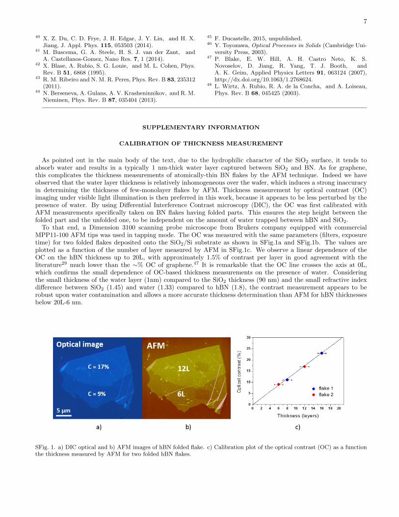
As pointed out in the main body of the text, due to the hydrophilic character of the SiO2 surface, it tends toabsorb water and results in a typically 1 nm-thick water layer captured between SiO2 and BN. As for graphene,this complicates the thickness measurements of atomically-thin BN flakes by the AFM technique. Indeed we haveobserved that the water layer thickness is relatively inhomogeneous over the wafer, which induces a strong inaccuracyin determining the thickness of few-monolayer flakes by AFM. Thickness measurement by optical contrast (OC)imaging under visible light illumination is then preferred in this work, because it appears to be less perturbed by thepresence of water. By using Differential Interference Contrast microscopy (DIC), the OC was first calibrated withAFM measurements specifically taken on BN flakes having folded parts. This ensures the step height between thefolded part and the unfolded one, to be independent on the amount of water trapped between hBN and SiO2.
To that end, a Dimension 3100 scanning probe microscope from Brukers company equipped with commercialMPP11-100 AFM tips was used in tapping mode. The OC was measured with the same parameters (filters, exposuretime) for two folded flakes deposited onto the SiO2/Si substrate as shown in SFig.1a and SFig.1b. The values areplotted as a function of the number of layer measured by AFM in SFig.1c. We observe a linear dependence of theOC on the hBN thickness up to 20L, with approximately 1.5% of contrast per layer in good agreement with theliterature29 much lower than the ∼% OC of graphene.47 It is remarkable that the OC line crosses the axis at 0L,which confirms the small dependence of OC-based thickness measurements on the presence of water. Consideringthe small thickness of the water layer (1nm) compared to the SiO2 thickness (90 nm) and the small refractive indexdifference between SiO2 (1.45) and water (1.33) compared to hBN (1.8), the contrast measurement appears to berobust upon water contamination and allows a more accurate thickness determination than AFM for hBN thicknessesbelow 20L-6 nm.
SFig. 1. a) DIC optical and b) AFM images of hBN folded flake. c) Calibration plot of the optical contrast (OC) as a functionthe thickness measured by AFM for two folded hBN flakes.

8
THE LOW-DIMENSIONALITY EFFECT IS NOT SAMPLE-DEPENDENT
SFig. 2. CL spectra of 6L mechanically exfoliated hBN flakes obtained from a) Saint-Gobain powder b) NIMS sample. Spectraare corrected from the spectral response of the detection system.

9
PHONON REPLICAS
SFig. 3. CL spectra of hBN flakes of 24L (red) and 30L (blue, SEM image in inset) exfoliated from the Saint-Gobain powder.Note that the spectra are plotted in logarithmic scale.
Recorded using higher exposure time, the CL spectra of SFig. 3 exhibit lower energy replicas of S1 and S3-4lines. Associated with the S1 emission at 5.903eV, we detect peaks at 5.730eV, 5.559eV and 5.392eV with decreasingintensities. The peaks are shifted by a constant energy value of ∼171 meV. This energy almost exactly corresponds tothe 169 meV energy of the LO phonon (Raman-active) mode E2g of hBN. This mode is related to in-plane vibrationsthat is the reason why the number of hBN layers does not affect significantly its energy as shown experimentally29
and theoretically.48 In SFig. 3, we also observe the phonon replicas of the S3-4 lines already reported in our previousstudy.13
10
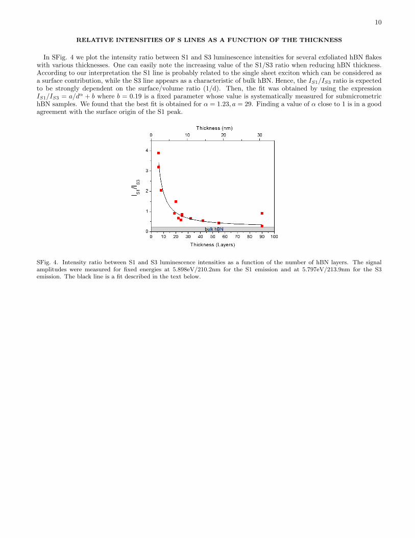
RELATIVE INTENSITIES OF S LINES AS A FUNCTION OF THE THICKNESS
In SFig. 4 we plot the intensity ratio between S1 and S3 luminescence intensities for several exfoliated hBN flakeswith various thicknesses. One can easily note the increasing value of the S1/S3 ratio when reducing hBN thickness.According to our interpretation the S1 line is probably related to the single sheet exciton which can be considered asa surface contribution, while the S3 line appears as a characteristic of bulk hBN. Hence, the IS1/IS3 ratio is expectedto be strongly dependent on the surface/volume ratio (1/d). Then, the fit was obtained by using the expressionIS1/IS3 = a/dα + b where b = 0.19 is a fixed parameter whose value is systematically measured for submicrometrichBN samples. We found that the best fit is obtained for α = 1.23, a = 29. Finding a value of α close to 1 is in a goodagreement with the surface origin of the S1 peak.
SFig. 4. Intensity ratio between S1 and S3 luminescence intensities as a function of the number of hBN layers. The signalamplitudes were measured for fixed energies at 5.898eV/210.2nm for the S1 emission and at 5.797eV/213.9nm for the S3emission. The black line is a fit described in the text below.

11
AFM CHARACTERIZATION OF THIN HBN FLAKES
SFig. 5. AFM images of exfoliated hBN layers transferred onto a SiO2/Si substrate composed of : a) 6L c) 8L and d) 20L. Theimage size unit is micrometer. Profile taken across the part of the 6L flake along the arrow is shown in b). The OC indicatesa 6L thickness while AFM exhibits 3.1 nm height revealing a 1nm water layer thickness trapped between hBN and SiO2.