diodes
TRANSCRIPT
7.1
PMcL Contents Index
2019 7 - Diodes
7 Diodes
Contents
Introduction ..................................................................................................... 7.2
7.1 The Silicon Junction Diode ....................................................................... 7.3 7.1.1 The Forward-Bias Region............................................................. 7.4 7.1.2 The Reverse-Bias Region ............................................................. 7.6
7.1.3 The Breakdown Region ................................................................ 7.6 7.1.4 Diode Symbol ............................................................................... 7.7
7.2 Breakdown Diodes .................................................................................... 7.7 7.2.1 Zener Breakdown.......................................................................... 7.7
7.2.2 Avalanche Breakdown .................................................................. 7.7
7.3 Other Types of Diode ................................................................................ 7.8 7.3.1 The Photodiode ............................................................................. 7.8 7.3.2 The Light Emitting Diode (LED) ................................................. 7.8
7.3.3 The Schottky Diode ...................................................................... 7.9 7.3.4 The Varactor Diode ...................................................................... 7.9
7.4 Analysis Techniques ................................................................................ 7.10
7.4.1 Graphical Analysis...................................................................... 7.10
7.4.2 Numerical Analysis .................................................................... 7.12
7.5 Summary .................................................................................................. 7.14
7.6 References ............................................................................................... 7.14

7.2
Index Introduction PMcL
7 - Diodes 2019
Introduction
Nonlinear circuits play a major role in modern electronics. Examples include
signal generators, communication transmitters and receivers, DC power
supplies, and digital circuits.
To begin a study of nonlinear circuits, we need to examine the most
fundamental two-terminal nonlinear device: the diode. The semiconductor
junction diode, or p-n junction diode, also forms the basis for other
semiconductor devices, such as the transistor.
The terminal characteristics of the diode will be presented, rather than the
underlying solid-state physics, so that we can focus on providing techniques for
the analysis of diode circuits. There are three types of diode circuit analysis
technique – graphical, numerical and use of a linear model. Graphical analysis
of diode circuits is done using graphs of the diode’s terminal characteristic and
the connected circuit. Numerical analysis can be performed with the nonlinear
equations of the diode with a technique known as iteration. Lastly, diodes can
be replaced with linear circuit models (of varying complexity), under assumed
diode operating conditions, so that we revert to linear circuit analysis. Each
analysis technique has its advantages and disadvantages, so it is important to
choose the most appropriate technique for a given circuit.

7.3
PMcL The Silicon Junction Diode Index
2019 7 - Diodes
7.1 The Silicon Junction Diode
A typical silicon p-n junction diode has the following i-v characteristic:
v
i(mA)
(V)0.60.40.2
2
4
6
8
10
forwardbias
reversebias
-0.2-150
(reverse saturation current)IS
= 1 nA
breakdown(large change in current,small change in voltage)
-VZK
Figure 7.1
The diode is clearly a nonlinear element – its characteristic is not a straight line
through the origin! The i-v characteristic can be divided up into three distinct
regions:
1. The forward-bias region, determined by 0v
2. The reverse-bias region, determined by 0v
3. The breakdown region, determined by ZKVv
7.4
Index The Silicon Junction Diode PMcL
7 - Diodes 2019
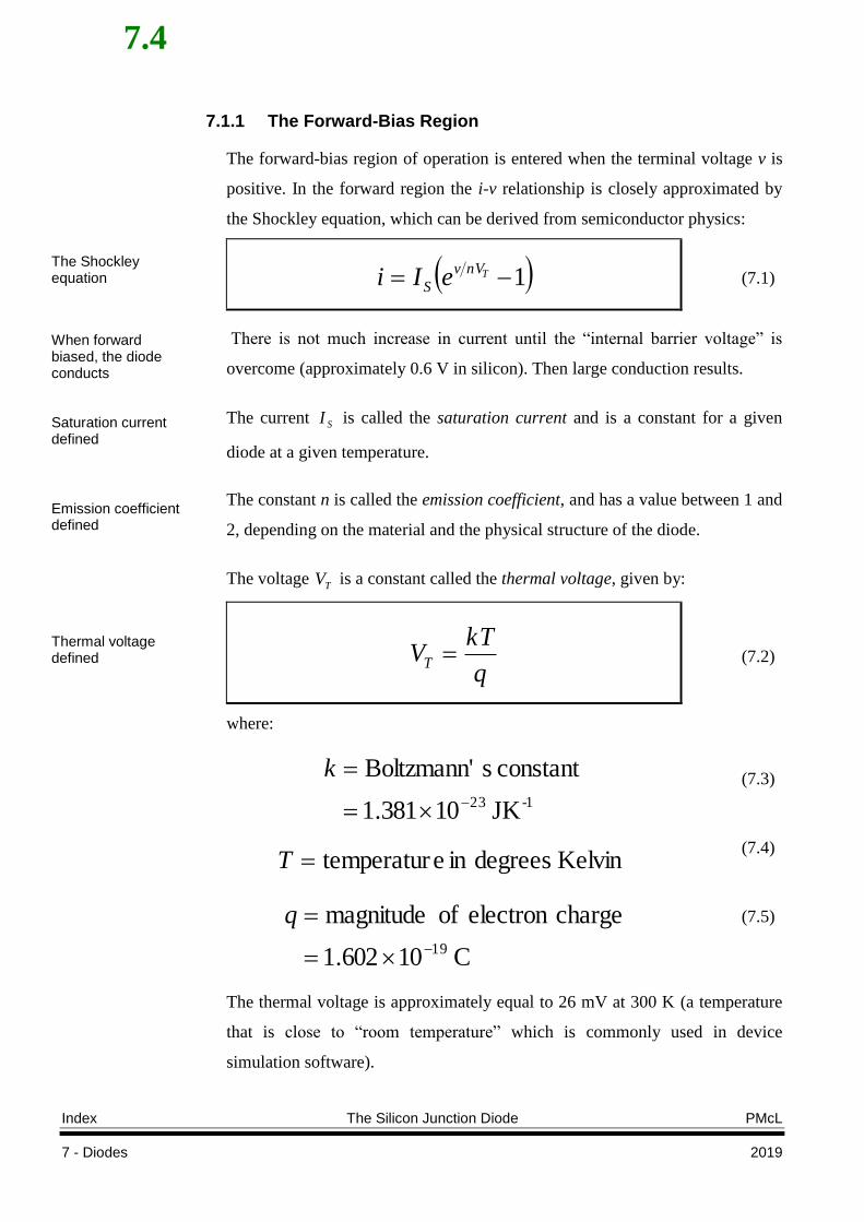
7.1.1 The Forward-Bias Region
The forward-bias region of operation is entered when the terminal voltage v is
positive. In the forward region the i-v relationship is closely approximated by
the Shockley equation, which can be derived from semiconductor physics:
1 TnVv
S eIi (7.1)
There is not much increase in current until the “internal barrier voltage” is
overcome (approximately 0.6 V in silicon). Then large conduction results.
The current SI is called the saturation current and is a constant for a given
diode at a given temperature.
The constant n is called the emission coefficient, and has a value between 1 and
2, depending on the material and the physical structure of the diode.
The voltage TV is a constant called the thermal voltage, given by:
q
kTVT
(7.2)
where:
1-23 JK 10381.1
constant sBoltzmann'
k
Kelvin degreesin etemperaturT
C 10602.1
chargeelectron of magnitude
19
q
(7.3)
(7.4)
(7.5)
The thermal voltage is approximately equal to 26 mV at 300 K (a temperature
that is close to “room temperature” which is commonly used in device
simulation software).
The Shockley equation
When forward biased, the diode conducts
Saturation current defined
Emission coefficient defined
Thermal voltage defined

7.5
PMcL The Silicon Junction Diode Index
2019 7 - Diodes
For appreciable current in the forward direction ( SIi ), the Shockley
equation can be approximated by:
TnVv
SeIi (7.6)
This equation is usually “good enough” for rough hand calculations when we
know that the current is appreciable.
From the characteristic we note that the current is negligibly small for v smaller
than about 0.5 V (for silicon). This value is usually referred to as the cut-in
voltage. This apparent threshold in the characteristic is simply a consequence
of the exponential relationship.
Another consequence of the exponential relationship is the rapid increase of
current for small changes in voltage. Thus for a “fully conducting” diode the
voltage drop lies in a narrow range, approximately 0.6 to 0.8 V for silicon. We
will see later that this gives rise to a simple model for the diode where it is
assumed that a conducting diode has approximately a 0.7 V drop across it
(again, for silicon).
The Shockley equation can be rearranged to give the voltage in terms of the
current:
1ln
S
TI
inVv
(7.7)
This logarithmic form is used in the numerical analysis of diode circuits.

7.6
Index The Silicon Junction Diode PMcL
7 - Diodes 2019
7.1.2 The Reverse-Bias Region
The reverse-bias region of operation is entered when the diode voltage v is
made negative. The Shockley equation predicts that if v is negative and a few
times large than TV in magnitude, the exponential term becomes negligibly
small compared to unity and the diode current becomes:
SIi (7.8)
That is, the current in the reverse direction is constant and equal to SI . This is
the reason behind the term saturation current. However, real diodes exhibit
reverse currents that, although quite small, are much larger than SI .
7.1.3 The Breakdown Region
The breakdown region is entered when the magnitude of the reverse voltage
exceeds a threshold value specific to the particular diode and called the
breakdown voltage. This is the voltage at the “knee” of the i-v curve and is
denoted by ZKV , where the subscript Z stands for Zener (to be explained
shortly) and K denotes knee.
Breakdown is not a destructive process unless the device cannot dissipate the
heat produced in the breakdown process. Breakdown is actually exploited in
certain types of diodes (e.g. the Zener diode) because of the near vertical
characteristic in this region.
When reverse biased, the diode does not conduct
Breakdown occurs eventually for a large enough reverse bias
7.7
PMcL Breakdown Diodes Index
2019 7 - Diodes
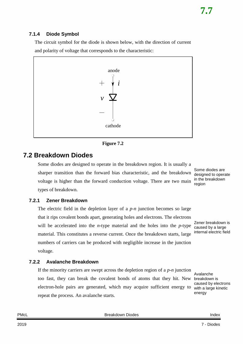
7.1.4 Diode Symbol
The circuit symbol for the diode is shown below, with the direction of current
and polarity of voltage that corresponds to the characteristic:
anode
cathode
v
i
Figure 7.2
7.2 Breakdown Diodes
Some diodes are designed to operate in the breakdown region. It is usually a
sharper transition than the forward bias characteristic, and the breakdown
voltage is higher than the forward conduction voltage. There are two main
types of breakdown.
7.2.1 Zener Breakdown
The electric field in the depletion layer of a p-n junction becomes so large
that it rips covalent bonds apart, generating holes and electrons. The electrons
will be accelerated into the n-type material and the holes into the p-type
material. This constitutes a reverse current. Once the breakdown starts, large
numbers of carriers can be produced with negligible increase in the junction
voltage.
7.2.2 Avalanche Breakdown
If the minority carriers are swept across the depletion region of a p-n junction
too fast, they can break the covalent bonds of atoms that they hit. New
electron-hole pairs are generated, which may acquire sufficient energy to
repeat the process. An avalanche starts.
Some diodes are designed to operate in the breakdown region
Zener breakdown is caused by a large internal electric field
Avalanche breakdown is caused by electrons with a large kinetic energy
7.8
Index Other Types of Diode PMcL
7 - Diodes 2019
7.3 Other Types of Diode
The silicon junction diode is not the only type of diode. A variety of diode
constructions exist, with many of them essential to the modern world, such as
the LED.
7.3.1 The Photodiode
In a photodiode, the p-n junction is very close to the surface of the crystal. The
Ohmic contact with the surface material is so thin, it is transparent to light.
Incident light (photons) can generate electron-hole pairs in the depletion layer
(a process called photoionisation).
7.3.2 The Light Emitting Diode (LED)
When a light-emitting diode is forward biased, electrons are able to recombine
with holes within the device, releasing energy in the form of light (photons).
The color of the light corresponds to the energy of the photons emitted, which
is determined by the “energy gap” of the semiconductor. LEDs present many
advantages over incandescent and compact fluorescent light sources including
lower energy consumption, longer lifetime, improved robustness, smaller size,
faster switching, and greater durability and reliability. At the moment LEDs
powerful enough for room lighting are relatively expensive and require more
precise current and heat management than compact fluorescent lamp sources of
comparable output.
LEDs are used in diverse applications. The compact size of LEDs has allowed
new text and video displays and sensors to be developed, while their high
switching rates are useful in advanced communications technology. Infrared
LEDs are also used in the remote control units of many commercial products
including televisions, DVD players, and other domestic appliances.
A photodiode is controlled by light
An LED emits photons when forward biased

7.9
PMcL Other Types of Diode Index
2019 7 - Diodes
7.3.3 The Schottky Diode
A Schottky diode is the result of a metal-semiconductor junction. The Schottky
diode is a much faster device than the general purpose silicon diode. There are
three main reasons for this: 1) the junction used is a metal-semiconductor
junction, which has less capacitance than a p-n junction, 2) often the
semiconductor used is gallium arsenide (GaAs) because electron mobility is
much higher, and 3) the device size is made extremely small. The result is a
device that finds applications in high speed switching.
7.3.4 The Varactor Diode
This device is also known as a variable capacitance diode. It has a relatively
large capacitance, brought about by a large junction area and narrow depletion
region. The applied reverse voltage changes the length of the depletion region,
which changes the capacitance. Thus, the device can be used in applications
that rely on a voltage controlled capacitance. Applications include electronic
tuning circuits used in communication circuits, and electronic filters.
A Schottky diode is a metal-semiconductor junction

7.10
Index Analysis Techniques PMcL
7 - Diodes 2019
7.4 Analysis Techniques
Since the diode’s characteristic is nonlinear, we can’t apply linear circuit
analysis techniques to circuits containing diodes. We therefore have to resort to
other analysis methods: graphical, numerical and linear modelling.
7.4.1 Graphical Analysis
Circuits with a single nonlinear element can always be modelled using the
Thévenin equivalent of the linear part:
iD
vD
VTh
RTh
linear
circuit
Thévenin equivalent circuit
iD
vD
Figure 7.3
KVL around the loop gives:
DThThD iRVv (7.9)
which, when rearranged to make iD the subject, gives:
ThD
Th
D VvR
i 1
(7.10)
When graphed, we call it the load line. It was derived from KVL, and so it is
always valid. The load line gives a relationship between iD and vD that is
determined purely by the external circuit. The diode’s characteristic gives a
relationship between iD and vD that is determined purely by the geometry and
physics of the diode.
The “load line” is derived using linear circuit theory

7.11
PMcL Analysis Techniques Index
2019 7 - Diodes
Since both the load line and the characteristic are to be satisfied, the only place
this is possible is the point at which they meet. This point is called the
quiescent point, or Q point for short:
Figure 7.4 – Graphical Analysis Using a Load Line
If the Thévenin voltage changes to ThV , then the operating point moves to Q
(the DC load line is shifted to the right).
The two end points of the load line are easily determined to enable quick
graphing. The two axis intercepts are:
Th
ThDD
R
Viv ,0
(7.11)
and:
0, DThD iVv (7.12)
Alternatively, we can graph the load line using one known point and the fact
that the slope is equal to ThR
1 .
The “load line” and device characteristic intersect at the Q
point

7.12
Index Analysis Techniques PMcL
7 - Diodes 2019
7.4.2 Numerical Analysis
Since, in the preceding analysis, we have two equations (the load line and the
diode characteristic) and two unknowns, it is tempting to try and solve them
simultaneously. If we substitute the voltage from the Shockley equation:
1ln
S
DTD
I
inVv
(7.13)
into the load line equation:
ThD
Th
D VvR
i 1
(7.14)
we get:
Th
S
DT
Th
D VI
inV
Ri 1ln
1
(7.15)
This equation is a transcendental equation, and its solution cannot be
expressed in term of elementary functions (try it!). With a sufficiently
advanced calculator (or mathematical software), we can use a special function
called the Lambert W function to solve it, but for engineering purposes, there
are usually simpler methods of solution.
We can solve transcendental equations graphically (as shown in the preceding
section) but we can also solve them numerically using a technique known as
iteration – which is suitable for computer simulations.

7.13
PMcL Analysis Techniques Index
2019 7 - Diodes
We begin with an initial “guess” for the diode current, labelled 0,Di , and then
compute:
3,
1,
2,
0,
1,
1ln1
1ln1
D
Th
S
D
T
Th
D
Th
S
D
T
Th
D
i
VI
inV
Ri
VI
inV
Ri
(7.16)
and so on until we get “convergence”, i.e. kDkD ii ,1, . Convergence is not
always guaranteed, and depends on the initial “guess”. Computer simulation
software uses several clever methods to aid in numerical convergence.
EXAMPLE 7.1 Numerical Analysis of a Circuit with a Real Diode
The following circuit contains a diode, with 1n and fA 030.2SI . We wish
to find the diode’s operating point, or Q point. Assume that mV 26TV .
iD
vD5 V
1 k
Starting with mA 10, Di we have:
mA 262.4511003.2
0043.0ln026.0
10
1
mA 3.4511003.2
001.0ln026.0
10
1
1532,
1531,
D
D
i
i
Since the second value is very close to the value obtained after the first
iteration, no further iterations are necessary, and the solution is mA 262.4Di
and V 7379.0Dv .

7.14
Index Summary PMcL
7 - Diodes 2019
7.5 Summary
The silicon junction diode forms the basis of modern electronics. It is a
device that effectively allows a current in only one direction.
The forward conduction region of practical silicon diodes is accurately
characterised by the Shockley equation:
1 TnVv
S eIi
Beyond a certain value of reverse voltage (that depends on the diode)
breakdown occurs, and current increases rapidly with a small
corresponding increase in voltage. This property is exploited in diodes
known as breakdown diodes.
A variety of diode constructions exist, with many of them essential to the
modern world, such as the LED.
Since the diode’s characteristic is nonlinear, we can’t apply linear circuit
analysis techniques to circuits containing diodes. We therefore have to
resort to other analysis methods: graphical, numerical and linear modelling
7.6 References
Sedra, A. and Smith, K.: Microelectronic Circuits, Saunders College
Publishing, New York, 1991.