dip8 & dso16-12 design guide v1.0_19mar2013 - infineon
TRANSCRIPT

N e v e r s t o p t h i n k i n g .
Power Management & Supply
ICE3Bxx65J(G)
C o o l S E T
® F 3 J i t t e r V e r s i o n D e s i g n G u i d e
( D I P - 8 & D S O - 1 6 / 1 2 )
A pp l i ca t i on No te , V1 .0 , Mar 2013

Published by Infineon Technologies AG 81726 Munich, Germany © 2013 Infineon Technologies AG All Rights Reserved. Legal Disclaimer The information given in this document shall in no event be regarded as a guarantee of conditions or characteristics. With respect to any examples or hints given herein, any typical values stated herein and/or any information regarding the application of the device, Infineon Technologies hereby disclaims any and all warranties and liabilities of any kind, including without limitation, warranties of non-infringement of intellectual property rights of any third party. Information For further information on technology, delivery terms and conditions and prices, please contact the nearest Infineon Technologies Office (www.infineon.com). Warnings Due to technical requirements, components may contain dangerous substances. For information on the types in question, please contact the nearest Infineon Technologies Office. Infineon Technologies components may be used in life-support devices or systems only with the express written approval of Infineon Technologies, if a failure of such components can reasonably be expected to cause the failure of that life-support device or system or to affect the safety or effectiveness of that device or system. Life support devices or systems are intended to be implanted in the human body or to support and/or maintain and sustain and/or protect human life. If they fail, it is reasonable to assume that the health of the user
or other persons may be endangered.

ICE3Bxx65J(G)
Revision History: 2013-03 V1.0
Previous Version:
Page Subjects (major changes since last revision)
CoolSET
® F3 Jitter Version Design Guide (DIP-8 & DSO-16/12):
License to Infineon Technologies Asia Pacific Pte Ltd AN-PS0076
Kyaw Zin Min Kok Siu Kam Eric
We Listen to Your Comments
Any information within this document that you feel is wrong, unclear or missing at all? Your feedback will help us to continuously improve the quality of this document. Please send your proposal (including a reference to this document) to:
ICE3Bxx65J(G)
Table of Contents Page
Application Note 4 2013-03-19
1 Introduction .............................................................................................................................. 5
2 List of Features ........................................................................................................................ 5
3 Package .................................................................................................................................... 6
4 Block Diagram .......................................................................................................................... 7
5 Typical Application Circuit ...................................................................................................... 8
6 Functional description and component design ...................................................................... 9 6.1 Startup time ............................................................................................................................... 9 6.2 Soft Start .................................................................................................................................... 9 6.2.1 Vcc capacitor ........................................................................................................................... 10 6.3 Low standby power - Active Burst Mode ................................................................................... 10 6.3.1 Entering Active Burst Mode ...................................................................................................... 10 6.3.2 Working in Active Burst Mode ................................................................................................... 11 6.3.3 Leaving Active Burst Mode ....................................................................................................... 12 6.3.4 Minimum VCC supply voltage during burst mode ....................................................................... 13 6.4 Low EMI noise ......................................................................................................................... 13 6.4.1 Frequency jittering .................................................................................................................... 13 6.4.2 Other suggestions to solve EMI issue ....................................................................................... 14 6.5 Tight control in maximum power (Propagation delay compensation) ......................................... 14 6.6 Protection Features .................................................................................................................. 15 6.6.1 Auto restart protection mode .................................................................................................... 15 6.6.2 Blanking Time for over load protection ...................................................................................... 15
7 Product portfolio of CoolSET®-F3 Jitter Version (DIP-8 & DSO-16/12) ................................ 16
8 Useful formula for the SMPS design ..................................................................................... 16
9 References ............................................................................................................................. 17

ICE3Bxx65J(G)
Application Note 5 2013-03-19
1 Introduction
The CoolSET®
- F3(Jitter Version), ICE3Bxx65J(G) is the further development of the third generation CoolSET
® -F3 with a frequency jitter feature for better EMI and BiCMOS technology to provide a wider Vcc
operating range and a lower controller power consumption. The switching frequency is running at 67 kHz and it targets for DVD player, set-top box, portable game console, white goods, smart meter, auxiliary power supply for server/PC, etc. This application note provides detail functional description of the new features. The description of all other functions and calculations are shown in the datasheet as well as in the application note “AN-PS0076”.
2 List of Features
650V Avalanche Rugged CoolMOS® with built in Startup Cell
Active Burst Mode for lowest Standby Power @ light load controlled by Feedback Signal
Fast Load Jump Response in Active Burst Mode
67 kHz fixed Switching Frequency
Auto Restart Mode for Over temperature Detection
Auto Restart Mode for Over voltage Detection
Auto Restart Mode for Over load and Open Loop
Auto Restart Mode for VCC Under voltage
User defined Soft Start
Minimum of external Components required
Max Duty Cycle 75%
Overall Tolerance of Current Limiting < ±5%
Internal Leading Edge Blanking
BiCMOS technology provides wide VCC Range
Frequency Jittering for Low EMI

ICE3Bxx65J(G)
Application Note 6 2013-03-19
3 Package
The package for F3(Jitter Version) ICE3Bxx65J product is DIP-8.
Figure 1 Pin configuration - ICE3Bxx65J
The package for F3(Jitter Version) ICE3Bxx65JG product is DSO-16/12
10
11
12
9
VCCSoftS
FB
CS
N.C
N.C
GND
N.C.
Drain
Drain
8
7
3
2
1
4
Drain
Drain
5
6
Figure 2 Pin configuration - ICE3Bxx65JG
1 at Tj=110°C
Pin Name Description
1 SoftS Soft-Start
2 FB Feedback
3 CS Current Sense/650V CoolMOS® Source
4 Drain 650V1 CoolMOS
® Drain
5 Drain 650V1 CoolMOS
® Drain
6 N.C Not Connteced
7 VCC Controller Supply Voltage
8 GND Controller Ground
Pin Name Description
1 N.C. Not Connected
2 SoftS Soft-Start
3 FB FeedBack
4 CS Current Sense/650V CoolMOS® Source
5 Drain 650V1 CoolMOS
® Drain
6 Drain 650V1 CoolMOS
® Drain
7 Drain 650V1 CoolMOS
® Drain
8 Drain 650V1 CoolMOS
® Drain
9 N.C. Not Connected
10 N.C. Not Connected
11 VCC Controller Supply Voltage
12 GND Controller Ground
ICE3Bxx65J(G)
Application Note 7 2013-03-19
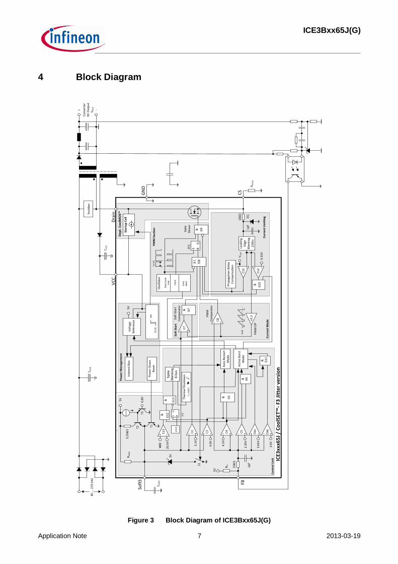
4 Block Diagram
Figure 3 Block Diagram of ICE3Bxx65J(G)
Inte
rnal
Bia
sV
olt
age
Ref
eren
ce
Osc
illat
or
Du
ty C
ycle
max
x3.2
Soft
-Sta
rt
Co
mp
arat
or
Cu
rre
nt
Lim
itin
g
PW
M O
P
Cu
rre
nt
Mo
de
Soft
Sta
rt
C2
3.1
V
RFB
Po
we
r M
anag
em
en
t
CSo
ftS
CV
CC
85
... 2
70
VA
CC
Bu
lk
+
Co
nve
rter
DC
Ou
tpu
tV
OU
T
Sp
ike
Bla
nkin
g
8.0
us
PW
M
Co
mp
arat
or
C3
4.0
V
C4
4.5
V
RSo
ftS
Gat
e D
rive
r
0.7
5
Clo
ck
RSe
nse
0.6
V1
0k D1
T2
C6
a
3.0
V
C5
1.3
5V
C1
0
RS
Q
Au
to R
esta
rt
Mo
de
& G7
& G5
& G9
1
G8
Ther
mal
Sh
utd
ow
n
T j >
14
0°C
3.2
5k
3V
S1
5V
T1P
ow
er-D
ow
n
Res
et
CS
Soft
SG
ND
C7
C8
FB
PW
M S
ect
ion
Co
ntr
ol U
nit
FF1
T3
C1
2&
0.3
2V
Lead
ing
Edge
B
lan
kin
g 220ns
25
k
2p
F
5V
G1
0
0.8
V
1p
F
Pro
pag
atio
n-D
elay
C
om
pen
sati
on
5V
Un
der
volt
age
Lock
ou
t1
8V
10
.3V
Vcs
th
-
ICE3
xxx6
5J
/ CoolSET™
- F3
Jit
ter
vers
ion
VC
CD
rain
De
pl.
CoolM
OS™
Star
tup
Ce
ll
C6
b
& G6
3.6
1V
& G1
1
Act
ive
Bu
rst
Mo
de
C1
32
0.5
V
VC
C&
G1
2
Freq
Ji
tter
Snu
bb
er
& G1
3
FF2
RSQ
UV
LO

ICE3Bxx65J(G)
Application Note 8 2013-03-19
5 Typical Application Circuit
Figure 4 Typical application circuit with ICE3B0565J 12W 5V
5V
/2.4
A
GN
D
F1
0.5
A
C1
0.1
uF/2
75
V
EM
I
2 x
27
mH
, 0
.5A
BR
1 2K
BB
40
+C
2
47u
F/4
00V
R1
150
k/2
W
D1
UF
40
05
C3
2n2
F/4
00V
21
34
IC2
SF
H61
7A
-3
C7
1uF
+
C5
22u
/25
V
C6
0.1
u
D2
1N
41
48
R2
510
R
Rc
6
470
R4
1.5
R
IC3
TL4
31
Cc
21
nF
Rc
46
.8k
Cc
11
uF
Rc
20
R Rc
31
0k
D2
1
SB
540
+C
21
180
0u
F/2
5V
L21
1.5
uH
+C
22
220
uF
/25V
85V
- 2
65V
ac
L1
L N
Sof
tst
VC
C
GN
D
DR
AIN
3
1
2
4
7
8
FB
Isen
se
DR
AIN5
IC1
ICE
3B
05
65
J
Rc
52
.2K
Rc
1
10k
C4
2.2
nF/2
50
V, Y
1
65 4
8
1 23
TR
1
EF
20
C8
1nF
24V
ZD
1
R4
A
15R
Rc
3A
*
C2
3*
R2
1*

ICE3Bxx65J(G)
Application Note 9 2013-03-19
6 Functional description and component design
6.1 Startup time
Startup time is counted from applying input voltage to IC turn on. ICE3Bxx65J(G) has a startup cell which is connected to input bulk capacitor. When there is input voltage, the startup cell will act as a constant current source to charge up the Vcc capacitor and supply energy to the IC. When the Vcc capacitor reaches the Vcc_on threshold 18V, the IC turns on. Then the startup cell is turned off and the Vcc is supplied by the auxiliary winding. Start up time is independent from the AC line input voltage and it can be calculated by the equation (1). Figure 4 shows the start up time of 85Vac line input.
where, IVCCcharge : 0.965mA (average current of IVCCcharge2 and IVCCcharge3)
VVCCon : IC turns on threshold ( 18V )
CVCC : Vcc capacitor
Please refer to the datasheet for the symbol used in the equation.
Channel 1; C1 : Drain voltage (VD)
Channel 2; C2 : Supply voltage (VCC)
Channel 3; C3 : Feedback voltage (VFB)
Channel 4; C4 : Soft Start voltage ( VSoftS )
Measured startup time = 490ms
Start-up @ 85Vac & max. load
Figure 5 The start-up time at AC line input voltage of 85Vac
Pre-caution : For a typical application, start up should be VCC ramps up first, other pin (such as FB pin) voltage will follow VCC voltage to ramp up. It is recommended not to have any voltage on other pins (such as FB; SoftS and CS) before VCC ramps up.
6.2 Soft Start
When the IC is turned on after the start-up time, the soft start capacitor at pin1, CSoftS is immediately charged up to approximately 0.8V and from this point IC starts switching. The soft start voltage VSoftS is generated by CSoftS and the internal pull up resistor RSoftS. The duty cycle of the gate drive is determined by the VSoftS during the soft start phase, which is terminated when VSoftS reaches 3.1V. Afterward, IC goes into normal mode and the duty cycle is dependent on the FB signal. The duration of the soft start can be estimated by the equation (2). Figure 6 shows the soft start behaviour at 85VAC input and full load. It can be seen that the primary peak current follows VSST voltage and slowly increase to the maximum. The soft start time is approximately 35.6ms.
where, Rsofts : internal soft start resistor (45kΩ)
Csofts : Soft start capacitor
490ms

ICE3Bxx65J(G)
Application Note 10 2013-03-19
Channel 1; C1 : Current sense voltage (VCS)
Channel 2; C2 : Supply voltage (VCC)
Channel 3; C3 : Feedback voltage (VFB)
Channel 4; C4 : Soft Start voltage ( VSoftS )
Soft Start time = 35.6ms
Soft start @ Vin=85Vac & max. load
Figure 6 Soft start at AC line input voltage of 85 Vac & full load
6.2.1 Vcc capacitor
The minimum value of the Vcc capacitor is determined by voltage drop during the soft start time. The formula is expressed in equation (3).
where, IVCCsup_g_max : supply current with active gate ( 3.6mA)
tss : soft start time ( 35.6ms )
CChysV : Vcc turn-on/off hysteresis voltage ( 7.7V )
Therefore, the minimum Vcc capacitance can be 11.09μF. In order to give more margins, 22uF is taken for the design. The startup time tStartUp is then 0.41s. The measured start up time is 0.49s (Figure 5). A 0.1uF filtering capacitor is always needed to add as near as possible to the Vcc pin to filter the high frequency noise.
6.3 Low standby power - Active Burst Mode
The IC will enter Active Burst Mode function at light load condition which enables the system to achieve the lowest standby power requirement of less than 100mW. Active Burst Mode means the IC is always in the active state and can therefore immediately response to any changes on the FB signal, VFB.
6.3.1 Entering Active Burst Mode
Because of the current mode control scheme, the feedback voltage VFB actually controls the power delivery to output. When the output load is getting lower, the feedback voltage VFB drops. If it stays below 1.35V for a timeframe set by the blanking time, the IC enters into the burst mode operation. The threshold power to enter burst mode is:
where, Lp : transformer primary inductance
VFBC5 : feedback level to enter burst mode (1.35V)
VMax-Ramp : voltage ramp offset (0.6V)
fs : switching frequency
AV : PWM OP gain (3.2)
csR : current sense resistor
35.6ms

ICE3Bxx65J(G)
Application Note 11 2013-03-19
Figure 7 shows the waveform with the load drops from nominal load to light load. After the 21ms blanking time IC goes into burst mode. The blanking time to enter burst mode is:
where, Rsofts : internal soft start resistor (45kΩ)
Csofts : Soft start capacitor
Channel 1; C1 : Drain voltage (VD)
Channel 2; C2 : Feedback voltage (VFB)
Channel 3; C3 : Soft Start voltage ( VSoftS )
Channel 4; C4 : Output voltage ( Vo )
Entering Active Burst mode with blanking time when load changes from full to light @ Vin=85Vac
Figure 7 Entering active burst mode
6.3.2 Working in Active Burst Mode
In the active burst mode, the IC is constantly monitoring the output voltage by feedback pin, VFB, which controls burst duty cycle and burst frequency. The burst “ON” starts when VFB reaches 3.61V and it stops
when VFB is dropped to 3V. During burst “ON”, the primary current limit is reduced to Vcs2 ( 32% of maximum peak current ) to reduce the conduction losses and to avoid audible noise. The FB voltage is swinging like a saw tooth between 3V and 3.61V. The corresponding secondary output ripple (peak to peak) is controlled to be small. It can be calculated by equation (6).
where, Ropto :series resistor with opto-coupler at secondary side (e.g. Rc6 in Figure 4)
Rfb :IC internal pull up resistor connected to FB pin (Rfb=14KΩ)
Gopto :current transfer gain of opto-coupler
GTL431 :voltage transfer gain of the loop compensation network (e.g. Rc1, Rc2, Rc3, Rc4, Rc5, Rc6, Cc1, Cc2 in Figure 4)
Vfb : feedback voltage change (0.61V)
Figure 8 is the output ripple waveform of the 12W 5V demo board. The burst ripple voltage is about 19mV.
Channel 1; C1 : Drain voltage (VD)
Channel 2; C2 : Feedback voltage (VFB)
Channel 4; C4 : Output ripple voltage (Vripple_pk_pk )
Vripple_pk_pk=60mV
Probe terminal end with decoupling capacitor of 0.1uF(ceramic) & 1uF(electrolytic), 20MHz filter
Output ripple voltage @ 85Vac and 0.5W load
Figure 8 Output ripple during Active Burst Mode at light load
21ms
ICE3Bxx65J(G)
Application Note 12 2013-03-19
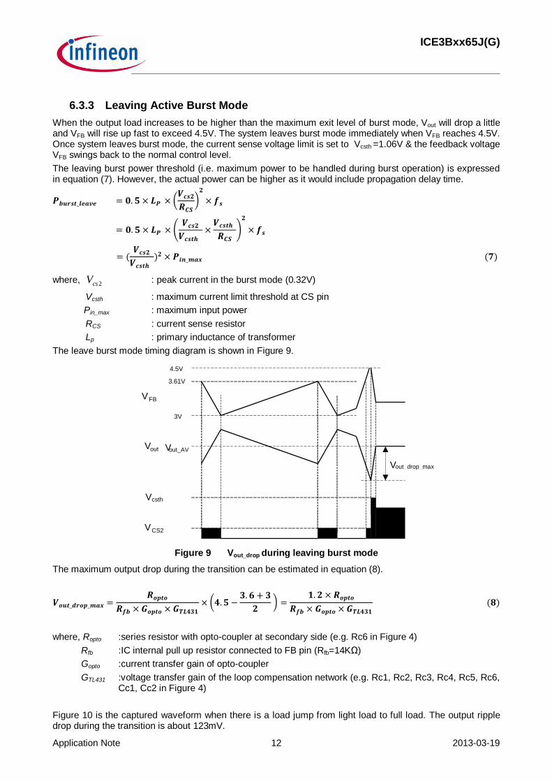
6.3.3 Leaving Active Burst Mode
When the output load increases to be higher than the maximum exit level of burst mode, Vout will drop a little and VFB will rise up fast to exceed 4.5V. The system leaves burst mode immediately when VFB reaches 4.5V. Once system leaves burst mode, the current sense voltage limit is set to Vcsth =1.06V & the feedback voltage VFB swings back to the normal control level.
The leaving burst power threshold (i.e. maximum power to be handled during burst operation) is expressed in equation (7). However, the actual power can be higher as it would include propagation delay time.
where, 2csV : peak current in the burst mode (0.32V)
Vcsth : maximum current limit threshold at CS pin
Pin_max : maximum input power
RCS : current sense resistor
Lp : primary inductance of transformer
The leave burst mode timing diagram is shown in Figure 9.
Figure 9 Vout_drop during leaving burst mode
The maximum output drop during the transition can be estimated in equation (8).
where, Ropto :series resistor with opto-coupler at secondary side (e.g. Rc6 in Figure 4)
Rfb :IC internal pull up resistor connected to FB pin (Rfb=14KΩ)
Gopto :current transfer gain of opto-coupler
GTL431 :voltage transfer gain of the loop compensation network (e.g. Rc1, Rc2, Rc3, Rc4, Rc5, Rc6, Cc1, Cc2 in Figure 4)
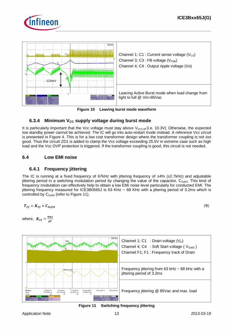
Figure 10 is the captured waveform when there is a load jump from light load to full load. The output ripple drop during the transition is about 123mV.
V FB
V out_AV
V out_drop_max
3.61V
3V
V out
4.5V
V CS2
Vcsth
ICE3Bxx65J(G)
Application Note 13 2013-03-19
Channel 1; C1 : Current sense voltage (VCS)
Channel 3; C3 : FB voltage (VFBB)
Channel 4; C4 : Output ripple voltage (Vo)
Leaving Active Burst mode when load change from light to full @ Vin=85Vac
Figure 10 Leaving burst mode waveform
6.3.4 Minimum VCC supply voltage during burst mode
It is particularly important that the Vcc voltage must stay above VVCCoff (i.e. 10.3V). Otherwise, the expected low standby power cannot be achieved. The IC will go into auto-restart mode instead. A reference Vcc circuit is presented in Figure 4. This is for a low cost transformer design where the transformer coupling is not too good. Thus the circuit ZD1 is added to clamp the Vcc voltage exceeding 25.5V in extreme case such as high load and the Vcc OVP protection is triggered. If the transformer coupling is good, this circuit is not needed.
6.4 Low EMI noise
6.4.1 Frequency jittering
The IC is running at a fixed frequency of 67kHz with jittering frequency of ±4% (±2.7kHz) and adjustable jittering period in a switching modulation period by changing the value of the capacitor, CSoftS. This kind of frequency modulation can effectively help to obtain a low EMI noise level particularly for conducted EMI. The jittering frequency measured for ICE3B0565J is 63 KHz ~ 68 KHz with a jittering period of 3.2ms which is controlled by CSoftS (refer to Figure 11).
where,
Channel 1; C1 : Drain voltage (VD)
Channel 4; C4 : Soft Start voltage ( VSoftS )
Channel F1; F1 : Frequency track of Drain
Frequency jittering from 63 kHz ~ 68 kHz with a jittering period of 3.2ms
Frequency jittering @ 85Vac and max. load
Figure 11 Switching frequency jittering
123mV
ICE3Bxx65J(G)
Application Note 14 2013-03-19
6.4.2 Other suggestions to solve EMI issue
Some more suggestions to improve the EMI performance are listed below.
1. Add RCD clamper circuit to the primary winding of the transformer: RCD clamper circuit (D1, R1 & C3) can absorb the current due to leakage inductance of transformer during switch off time of the MOSFET, so voltage spike of the drain can clamp to desired voltage level and suppress the EMI noise (refer to Figure 4).
2. Add capacitor (CDS) at the drain source pin: CDS can slow down the turn off speed of the MOSFET and the high ΔV/Δt noise will be reduced and so is the EMI noise. The drawback is more energy will be dissipated due to slower turn off speed of MOSFET.
3. Add snubber circuit to the output rectifier: Most of the radiated EMI noise comes out from the output of the system especially for a system with output cable. Adding snubber circuit (R21 and C23) to the output rectifier is a more direct way to suppress those EMI noise (refer to Figure 4).
4. Reduce the reflection voltage: if the secondary to primary reflection voltage is reduced, the switching voltage at drain can also be reduced. Hence the voltage switching noise is reduced and so is the EMI noise. The drawback is the reverse voltage of the secondary rectifier will increase.
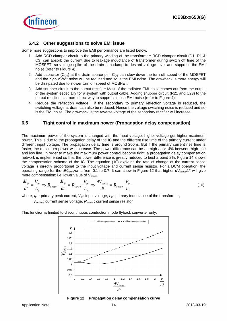
6.5 Tight control in maximum power (Propagation delay compensation)
The maximum power of the system is changed with the input voltage; higher voltage got higher maximum power. This is due to the propagation delay of the IC and the different rise time of the primary current under different input voltage. The propagation delay time is around 200ns. But if the primary current rise time is faster, the maximum power will increase. The power difference can be as high as >14% between high line and low line. In order to make the maximum power control become tight, a propagation delay compensation network is implemented so that the power difference is greatly reduced to best around 2%. Figure 14 shows the compensation scheme of the IC. The equation (10) explains the rate of change of the current sense voltage is directly proportional to the input voltage and current sense resistor. For a DCM operation, the operating range for the dVsense/dt is from 0.1 to 0.7. It can show in Figure 12 that higher dVsense/dt will give more compensation; i.e. lower value of Vsense.
p
in
sense
sense
p
in
sense
p
sense
p
inp
L
VR
dt
dV
L
VR
dt
dIR
L
V
dt
dI (10)
where, Ip : primary peak current, Vin : input voltage, Lp : primary inductance of the transformer,
Vsense : current sense voltage, Rsense : current sense resistor
This function is limited to discontinuous conduction mode flyback converter only.
0,9
0,95
1
1,05
1,1
1,15
1,2
1,25
1,3
0 0,2 0,4 0,6 0,8 1 1,2 1,4 1,6 1,8 2
with compensation without compensation
dt
dVSense s
V
Sen
seV
V
Figure 12 Propagation delay compensation curve

ICE3Bxx65J(G)
Application Note 15 2013-03-19
6.6 Protection Features
Protection is one of the major factors to determine whether the system is safe and robust. Therefore sufficient protection is necessary. A list of protections and the failure conditions are shown in the following table.
Protection function Failure condition Protection Mode
Vcc over-voltage Vcc > 20.5V & VSoftS < 4V & VFB > 4.5V & last for 8μs Auto Restart Mode
Over-temperature
(controller junction) TJ > 140°C & last for 8μs Auto Restart Mode
Over-load / Open loop VFB > 4.5V & VSOFTS > 4V (blanking time counted from charging CSST from (3.2V~3.6V to 4V )
Auto Restart Mode
Vcc under-voltage /
short opto-coupler Vcc < 10.3V Auto Restart Mode
6.6.1 Auto restart protection mode
When the failure condition meets the auto restart protection mode, the IC will go into auto restart. The switching pulse will stop. Then the Vcc voltage will drop. When the Vcc voltage drops to 10.3V, the startup cell will turn on again. The Vcc voltage is then charged up. When it hits 18V, the IC will turn on and the startup cell will turn off. It would then start the startup phase with soft start. After the startup phase the failure condition is checked to determine whether the fault persists. If the fault is removed, it will go to normal operation. Otherwise, the IC will repeat the auto restart protection and the switching pulse stop again.
6.6.2 Blanking Time for over load protection
The IC controller provides a blanking window before entering into the auto restart mode due to output overload/short circuit. The purpose is to ensure that the system will not enter protection mode unintentionally. The blanking time calculation for overload protection is same as active burst mode blanking window (equation 5).
Channel 1; C1 : Drain voltage (VD)
Channel 2; C2 : Supply voltage (VCC)
Channel 3; C3 : Feedback voltage (VFB)
Channel 4; C4 : Soft Start voltage ( VSoftS )
Blanking time =21ms
Over load protection with blanking time @ 85Vac
Figure 13 blanking window for over load protection

ICE3Bxx65J(G)
Application Note 16 2013-03-19
7 Product portfolio of CoolSET®-F3 Jitter Version (DIP-8 & DSO-16/12)
Device Package VDS Frequency / kHz Rdson /Ω1 230Vac±15%
2 85-265Vac
2
ICE3B0365J PG-DIP-8 650V 67 6.45 22W 10W
ICE3B0565J PG-DIP-8 650V 67 4.70 25W 12W
ICE3B1565J PG-DIP-8 650V 67 1.70 42W 20W
ICE3B2065J PG-DIP-8 650V 67 0.92 57W 28W
ICE3B0365JG PG-DSO-16/12 650V 67 6.45 22W 10W
ICE3B0565JG PG-DSO-16/12 650V 67 4.70 25W 12W
8 Useful formula for the SMPS design
Transformer ( DCM flyback)
Input data
, ,
Drain to source voltage composition
Turn ratio
Duty maximum
Primary Inductance
Primary peak current
Primary rms current
Primary turns
1 Typ @ 25°C
2 Calculated maximum input power rating at Ta=75°C, Tj=125°C and without copper area as heat sink.

ICE3Bxx65J(G)
Application Note 17 2013-03-19
Secondary turns
Auxiliary turns
ICE3Bxx65J(G) other components
Current sense resistor
Soft start time
Vcc capacitor
Startup time
Enter burst mode power
Output ripple during burst mode
Leave burst mode power
Blanking time for over
load protection/ active burst mode
9 References
[1] Infineon Technologies, Datasheet “CoolSET®-F3(Jitter Version) ICE3Bxx65J Off-Line SMPS Current
Mode Controller with Integrated 650V CoolMOS® and Startup Cell in DIP-8”
[2] Infineon Technologies, Datasheet “CoolSET®-F3(Jitter Version) ICE3Bxx65JG Off-Line SMPS Current
Mode Controller with Integrated 650V CoolMOS® and Startup Cell in DSO-16/12”
[3] Kok Siu Kam Eric, Jeoh Meng Kiat, Infineon Technologies, Application Note “AN-EVALSF3-ICE3B0565J, 12W 5V SMPS Evaluation Board with CoolSET
®-F3 ICE3B0565J”
[4] Kyaw Zin Min, Kok Siu Kam Eric, He Yi, Jeoh Meng Kiat, Infineon Technologies, Application Note “AN-EVALSF3-ICE3B0365J, 5W 2 outputs (5V & 18V) DC/DC SMPS Demo Board with CoolSET
®-F3
ICE3B0365J”