direct digital synthesis - ieeesites.ieee.org/scv-cas/files/2013/02/2012galanopoulos.pdf · ·...
TRANSCRIPT

1
All-Digital Transmitter
IEEE Santa Clara Valley Circuits & Systems Society
January 16, 2012
Kostas GalanopoulosPh.D. Candidate
Dept. of Electrical and Computer EngineeringNational Technical University of Athens, Greece
Affiliate, SOTEKCO Electronics LLC, USA [email protected]
Supervisor: Prof. Paul P. SotiriadisSOTEKCO Electronics LLC, USA

2
All-Digital Transmitter
• Theoretical overview of the proposed techniques:
• Direct All-Digital Synthesis
• Spurs Reduction Using Dithering
• All-Digital modulation techniques
• Nearly All-Digital analog data acquisition
• Live demo presentation:
• FM radio transmitter
• AM radio transmitter
This is the first implementation of a practical and purely digital rf
transmitter.
Presentation outline

3
What is an All-Digital Transmitter?
• Radio transmitter with (ideally) no analog components.
• Based on Direct All-Digital Frequency Synthesis & Modulation techniques.
• Inputs: A) Clock signal, B) Digital Data sequence
• Output: 1-bit digital sequence driving directly A) a (tuned) antenna, Or,
B) a switching (class-D) power RF amplifier.

4
Why All Digital Transmitter?
… compared to analog / mixed signal architectures
• Consumes significantly lower power
• Occupies significantly smaller chip area
• All advantages of digital circuit design
• portability, scalability, reconfigurability, CAD tools ( VHDL/Verilog - layout (APR) - test flow (BIST) )
• Very short concept-to-market time.
• Compact, relatively simple, flexible architectures
Advantages
5
Why not All Digital Transmitter?Disadvantages
… compared to analog/ mixed signal architectures
• Worse Spurious Free Dynamic Range (SFDR) and/or noise floor
• Lower frequency range
6
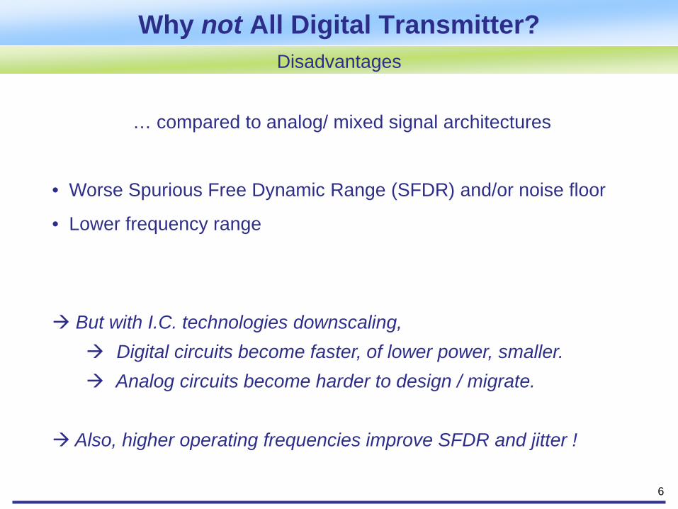
Why not All Digital Transmitter?Disadvantages
… compared to analog/ mixed signal architectures
• Worse Spurious Free Dynamic Range (SFDR) and/or noise floor
• Lower frequency range
But with I.C. technologies downscaling, Digital circuits become faster, of lower power, smaller. Analog circuits become harder to design / migrate.
Also, higher operating frequencies improve SFDR and jitter !
7
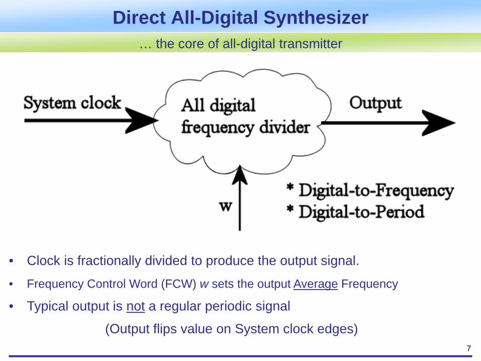
Direct All-Digital Synthesizer… the core of all-digital transmitter
• Clock is fractionally divided to produce the output signal.
• Frequency Control Word (FCW) w sets the output Average Frequency
• Typical output is not a regular periodic signal
(Output flips value on System clock edges)
8
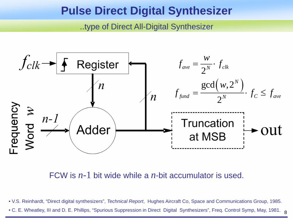
Pulse Direct Digital Synthesizer..type of Direct All-Digital Synthesizer
FCW is n-1 bit wide while a n-bit accumulator is used.
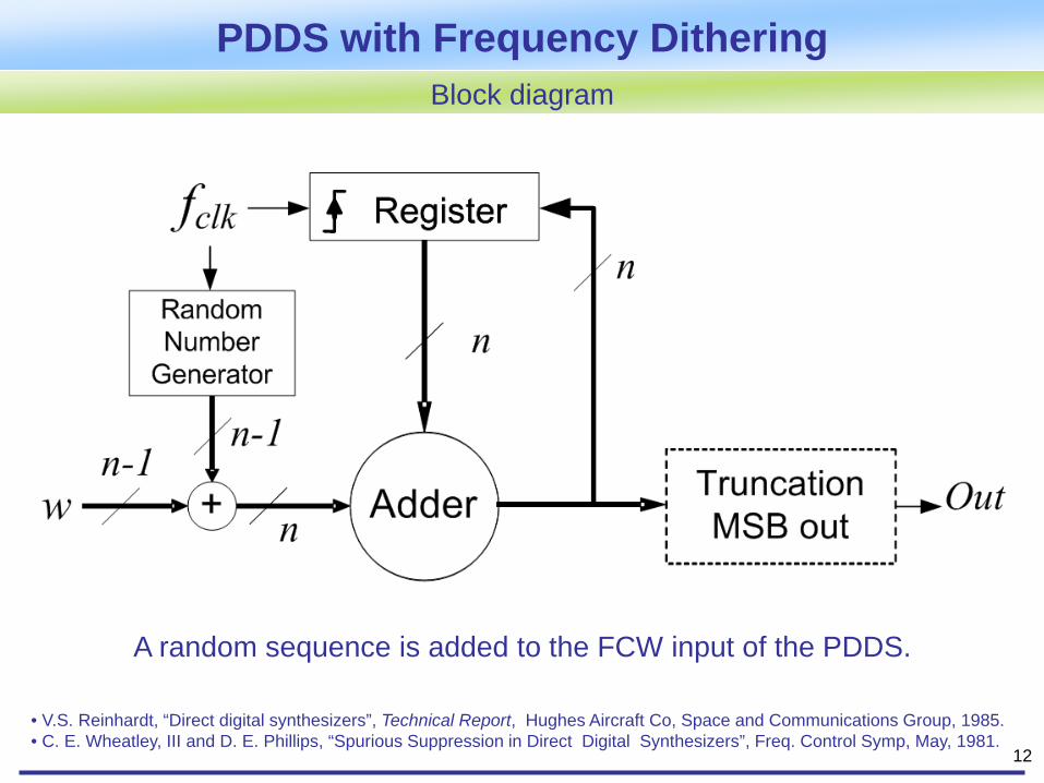
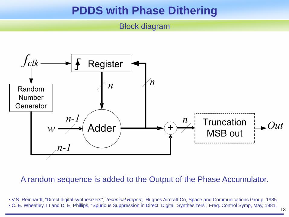
• V.S. Reinhardt, “Direct digital synthesizers”, Technical Report, Hughes Aircraft Co, Space and Communications Group, 1985.
• C. E. Wheatley, III and D. E. Phillips, “Spurious Suppression in Direct Digital Synthesizers”, Freq. Control Symp, May, 1981.
( )2gcd ,2
2
ave clkN
N
fund C aveN
wf f
wf f f
= ⋅
= ⋅ ≤

9
Pulse Direct Digital SynthesizerOutput Timing Irregularity
• PDDS is a synchronous FSM, so…
• Output has timing irregularities (deterministic jitter) for most frequencies
• (deterministic) Jitter ≤ ½ Clock Cycle.
fundamental output period
A:
B:
C:
average output period
one clock cycle(A) Ideal Output, (B) Output, (C) Clock

10
Output spectrum (simulation with a 16MHz clk)
Pulse Direct Digital Synthesizer
0 1M 2M 3M 4M 5M 6M 7M 8M6
-80
-70
-60
-50
-40
-30
-20
-10
0
Pow
er (d
B)
Frequency
• Timing irregularities imply many & strong (undesirable) frequency spurs!
11
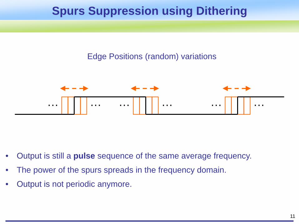
Edge Positions (random) variations
Spurs Suppression using Dithering
• Output is still a pulse sequence of the same average frequency.
• The power of the spurs spreads in the frequency domain.
• Output is not periodic anymore.
… …… …… …
12
• V.S. Reinhardt, “Direct digital synthesizers”, Technical Report, Hughes Aircraft Co, Space and Communications Group, 1985.• C. E. Wheatley, III and D. E. Phillips, “Spurious Suppression in Direct Digital Synthesizers”, Freq. Control Symp, May, 1981.
PDDS with Frequency DitheringBlock diagram
A random sequence is added to the FCW input of the PDDS.
13
• V.S. Reinhardt, “Direct digital synthesizers”, Technical Report, Hughes Aircraft Co, Space and Communications Group, 1985.• C. E. Wheatley, III and D. E. Phillips, “Spurious Suppression in Direct Digital Synthesizers”, Freq. Control Symp, May, 1981.
PDDS with Phase DitheringBlock diagram
A random sequence is added to the Output of the Phase Accumulator.
14
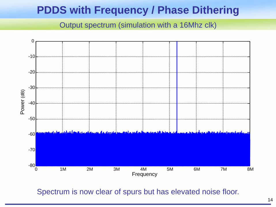
PDDS with Frequency / Phase Dithering
Spectrum is now clear of spurs but has elevated noise floor.
Output spectrum (simulation with a 16Mhz clk)
0 1M 2M 3M 4M 5M 6M 7M 8M-80
-70
-60
-50
-40
-30
-20
-10
0
Pow
er(d
B)
Frequency

15
Implementation MeasurementsUndithered PDDS output
In Xilinx Spartan 3e (Clk = 200Mhz)

16
Implementation Measurements
The implementation achieves a ~70dBc/Hz noise floor.
Dithered PDDS output
17
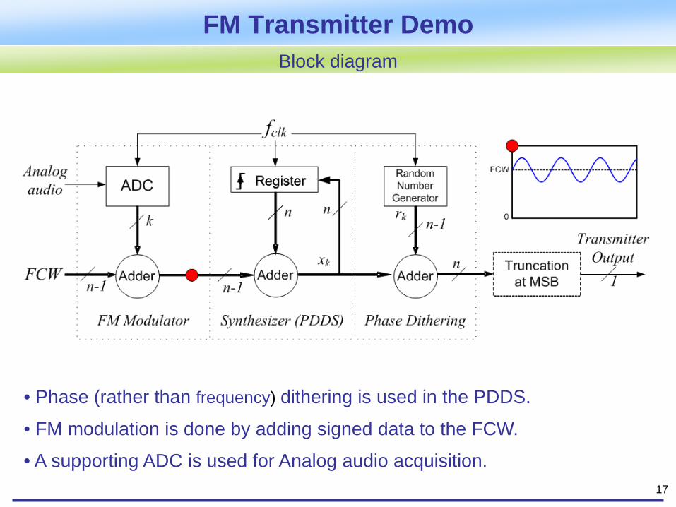
FM Transmitter DemoBlock diagram
• Phase (rather than frequency) dithering is used in the PDDS.
• FM modulation is done by adding signed data to the FCW.
• A supporting ADC is used for Analog audio acquisition.

18
Audio Data Acquisition
• It is supplementary; Ideally (only) a Digital Data steam should be used.
• 1-bit Oversampling ADC better fits to this “All-Digital application”.
• Only a couple of external Rs & Cs analog components are used.
Any ADC could be used, but we preferred a…

19
Dithering slightly effects the noise performance of the system.
System performance using a 12bit ADC
FM Transmitter Demo
20
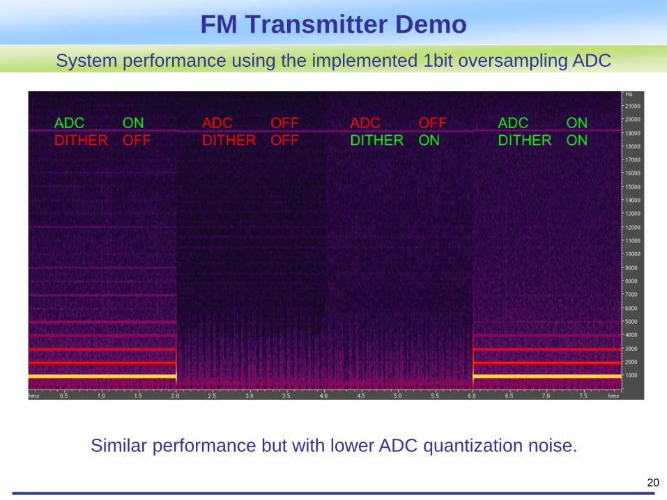
Similar performance but with lower ADC quantization noise.
System performance using the implemented 1bit oversampling ADC
FM Transmitter Demo

21
AM Transmitter DemoBlock diagram
• The carrier is generated using the 6 MSB of the dithered PDDS and a sine table.
• AM modulation is done by multiplying the Carrier with the unsigned audio data.
• The Transmitter output is generated by an All-digital 1bit oversampling DAC.
Typical DDS modulator

22
AM Transmitter DemoOutput spectrum (carrier only passing through the 1bit oversampling DAC)
• Useful only for lower frequencies but offers better noise performance.
• Actual implementation achieves a noise floor of ~90dbc/Hz for generated frequencies up to 5Mhz using a 200Mhz input clock.
10K 50K 100K 500K 1M 5M-100
-90
-80
-70
-60
-50
-40
-30
-20
-10
0
Pow
er (d
B)
Frequency
23
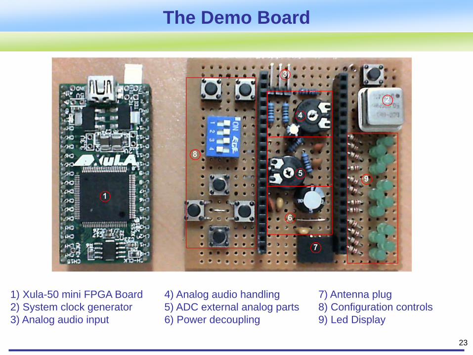
The Demo Board
1) Xula-50 mini FPGA Board2) System clock generator3) Analog audio input
4) Analog audio handling5) ADC external analog parts6) Power decoupling
7) Antenna plug8) Configuration controls9) Led Display
24
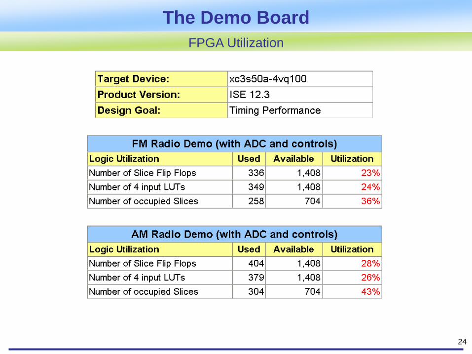
The Demo BoardFPGA Utilization
25
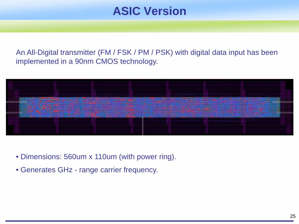
ASIC Version
An All-Digital transmitter (FM / FSK / PM / PSK) with digital data input has been implemented in a 90nm CMOS technology.
• Dimensions: 560um x 110um (with power ring).
• Generates GHz - range carrier frequency.
26
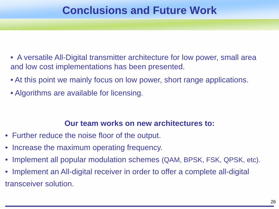
Conclusions and Future Work
Our team works on new architectures to:• Further reduce the noise floor of the output.• Increase the maximum operating frequency.• Implement all popular modulation schemes (QAM, BPSK, FSK, QPSK, etc).
• Implement an All-digital receiver in order to offer a complete all-digital transceiver solution.
• A versatile All-Digital transmitter architecture for low power, small area and low cost implementations has been presented.
• At this point we mainly focus on low power, short range applications.
• Algorithms are available for licensing.

27
Thank you for attending
Questions and related communication are very welcome!
Kostas GalanopoulosPh.D. Candidate
Dept. of Electrical and Computer EngineeringNational Technical University of Athens, Greece
Affiliate, SOTEKCO Electronics LLC, USA [email protected]
28
* M. H. Perrott 2009
*
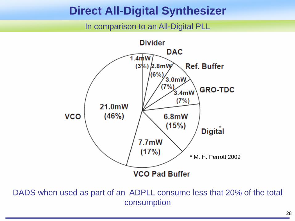
In comparison to an All-Digital PLL
DADS when used as part of an ADPLL consume less that 20% of the total consumption
Direct All-Digital Synthesizer