distance image sensors (back-thinned type) … · type no. s15452-01wt s15453-01wt s15454-01wt...
TRANSCRIPT
1
Distance image sensors (Back-thinned type) S15452/S15453/S15454-01WT
Contents 1. Features ........................................................................................................................................................... 1 2. Structure .......................................................................................................................................................... 2 3. Operating principle ........................................................................................................................................... 3
3-1. Indirect TOF (time-of-flight) ...................................................................................................................... 3 3-2. Background light elimination circuit .......................................................................................................... 6 3-3. Distance calculation ................................................................................................................................... 8 3-4. Charge drain function .............................................................................................................................. 12 3-5. Non-destructive readout .......................................................................................................................... 13 3-6. Drive timing ............................................................................................................................................. 14 3-7. Timing chart ............................................................................................................................................ 15 3-8. Calculating the frame rate ....................................................................................................................... 18
4. How to use ..................................................................................................................................................... 19 4-1. Configuration example ............................................................................................................................ 19 4-2. Light source selection .............................................................................................................................. 19
5. Calibration ...................................................................................................................................................... 20 6. Calculating the incident light level ................................................................................................................. 21 7. Evaluation kit .................................................................................................................................................. 25
Distance image sensors are image sensors that measure the distance to the target object using the TOF (time-of-flight) method. Used in combination with a pulse modulated light source, these sensors output delay time signals on the timing that the light is emitted and received. The sensor signals are arithmetically processed by an external signal processing circuit or a PC to obtain distance data.
1. Features ・Wide spectral response range to near infrared ・Reduced effect of background light ・Compact wafer level package (WLP) type
技術資料 Technical note
2
[Table 1-1] Product lineup Type Linear Area
Type no. S15452-01WT S15453-01WT S15454-01WT Pixel height 50 m 50 m Pixel pitch 20 m 20 m 50 m Number of pixels 64 256 96 × 72 Fill factor 80% 70% Video data rate 5 MHz 10 MHz
2. Structure Back-thinned type distance image sensors consist of a photosensitive area, shift register, output buffer amplifier, bias generator, timing generator, and so on. The block diagram is shown in Figure 2-1. Distance image sensors are different from typical CMOS image sensors in the following manner.
・Pixel structure that allows high-speed charge transfer ・Outputs from two output terminals the voltages needed to calculate the distance
Like a typical CMOS image sensor, the output signal from the photosensitive area is processed by the sample-and-hold circuit or column gain amplifier circuit, scanned sequentially by the shift register, and read out as voltage output.
[Figure 2-1] Block diagram (a) S15452-01WT
KMPDC0738EA
VTX3
VTX2
VTX1pix_reset
phis
mclktrig
Vdd(A) GND(A)
GND(D)
Vout1
Vout2
dclk
Vr Vsf Vpg
Vdd(D)
A6
B6
C6B5
C5
B4C4
A5A1 B2 A3 A2
C2
C1
B3
B1
C3
Horizontal shift register
Sample-and-hold circuit
Bias�generator
Buffer amp
Photodiode array80 pixels
CLTX
CLTX
CLTX
3
(b) S15453-01WT
KMPDC0742EA
(c) S15454-01WT
KMPDC0744EA
3. Operating principle
3-1. Indirect TOF (time-of-flight) The timing chart of the photosensitive area of the distance image sensor is shown in Figure 3-1. Output voltages Vout1 and Vout2 obtained by applying charge-to-voltage conversion on accumulated charges Q1 and Q2 based on their integration capacitances Cfd1 and Cfd2 are expressed by equations (3-1) and (3-2).
Vout1 = Q1/Cfd1 = N × Iph × {(T0 - Td)/Cfd1} …(3-1) Vout2 = Q2/Cfd2 = N × Iph × (Td/Cfd2) …(3-2)
VTX3
VTX2
VTX1pix_reset
phis
mclktrig
Vdd(A) GND(A)
GND(D)
Vout1
Vout2
dclk
Vr Vsf Vpg
Vdd(D)
A6
B6
C6B5
C5
B4C4
A5A1 B2 A3 A2
C2
C1
B3
B1
C3
Horizontal shift register
Sample-and-hold circuit
Biasgenerator
Buffer amp
Photodiode array272 pixels
dclk
Vout1
Vout2reset
vsthst
ext_reset
mclk
Vr
Vpg
Vdd(A)
GND(A)
Vdd(D)
A3 A4B4 B5
B2
B1
C1
D1
A1
D2
C5C6C4
E2 E5E3
D5D6
B6 A6 A5
E6
C2
E4
Biasgenerator A2
Horizontal shift registerBuffer amp
Sample-and-hold circuit
Photodiode array104 × 80 pixels
(
Verti
cals
hift
regi
ster
4
Cfd1, Cfd2: integration capacitance of each output N: charge transfer clock count Iph: photocurrent T0: pulse width of output light Td: delay time
Delay time Td when Cfd1=Cfd2 in equations (3-1) and (3-2) is expressed by equation (3-3).
Td = {Vout2/(Vout1 + Vout2)} × T0 …(3-3)
Using the values (Vout1, Vout2) output according to the distance, distance D is expressed by equation (3-4). D = 1/2 × c × Td = 1/2 × c × {Vout2/(Vout1 + Vout2)} × T0 …(3-4)
c: speed of light (3 × 10⁸ m/s)
[Figure 3-1] Timing chart of photosensitive area
KMPDC0470EB
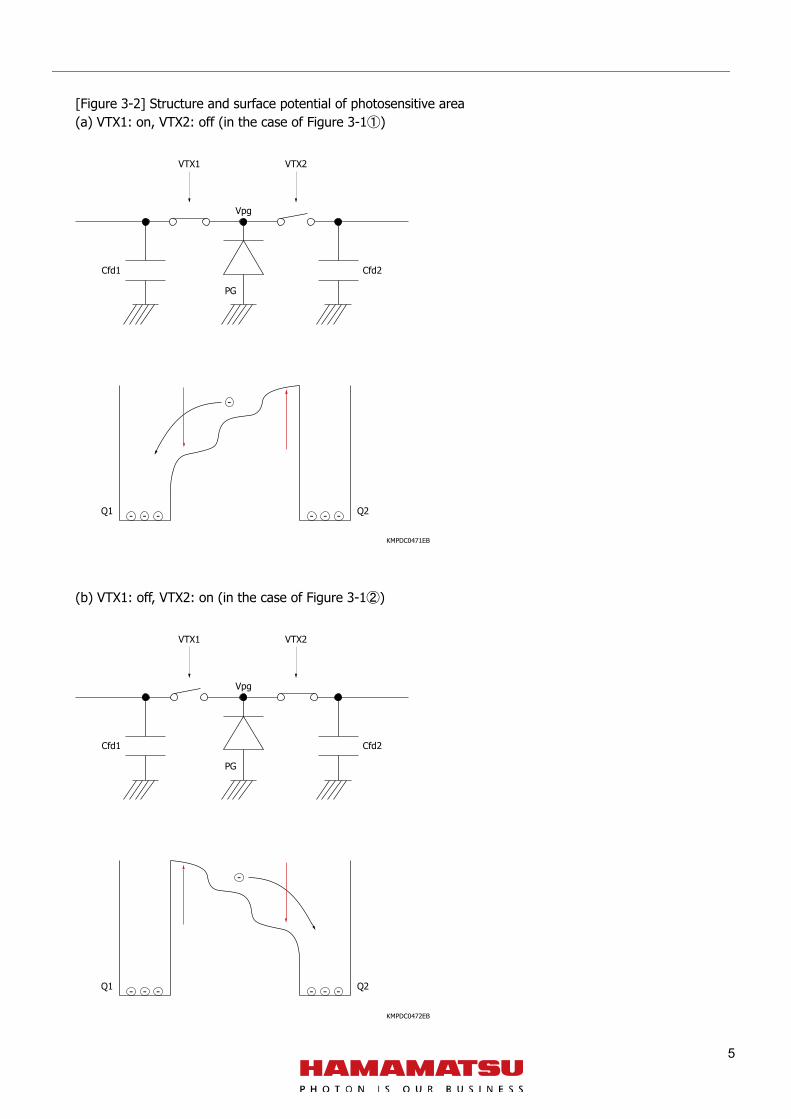
The structure and surface potential of the photosensitive area of the distance image sensor are shown in Figure 3-2. Typical CMOS image sensors can be driven with a single power supply, but the transfer time needed for the charge to move from the photosensitive area to the integration area is in the microsecond order. On the other hand, high-speed charge transfer (nanosecond order) is possible on CCD image sensors, but they require multiple voltage inputs including high voltage. To achieve the high-speed charge transfer (several tens of nanoseconds) needed to acquire distance information, we have developed a pixel structure that enables high-speed charge transfer like the CCDs in the CMOS process. This has allowed distance image sensors to achieve the high-speed charge transfer needed for distance measurement. The number of electrons generated in each pulse emission is several e-. Therefore, the operation shown in Figure 3-2 is repeated several thousand to several tens of thousands of times, and then the accumulated charge is read out. The number of repetitions varies depending on the incident light level and the required accuracy of distance measurement.
Q1
Td
VTX1
Reflected light
Pulse light
①
②
VTX2
T0
Q2
5
[Figure 3-2] Structure and surface potential of photosensitive area (a) VTX1: on, VTX2: off (in the case of Figure 3-1①)
KMPDC0471EB
(b) VTX1: off, VTX2: on (in the case of Figure 3-1②)
KMPDC0472EB
VTX1 VTX2
Vpg
Cfd1
Q1 Q2
Cfd2
PG
- -- - --
-
VTX1 VTX2
Vpg
Cfd1
Q1 Q2
Cfd2
PG
- -- - --
-
6
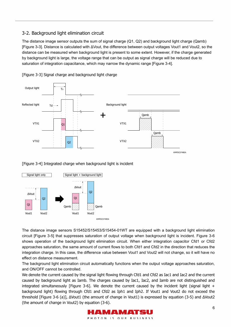
3-2. Background light elimination circuit The distance image sensor outputs the sum of signal charge (Q1, Q2) and background light charge (Qamb) [Figure 3-3]. Distance is calculated with ΔVout, the difference between output voltages Vout1 and Vout2, so the distance can be measured when background light is present to some extent. However, if the charge generated by background light is large, the voltage range that can be output as signal charge will be reduced due to saturation of integration capacitance, which may narrow the dynamic range [Figure 3-4].
[Figure 3-3] Signal charge and background light charge
KMPDC0748EA
[Figure 3-4] Integrated charge when background light is incident
KMPDC0749EA
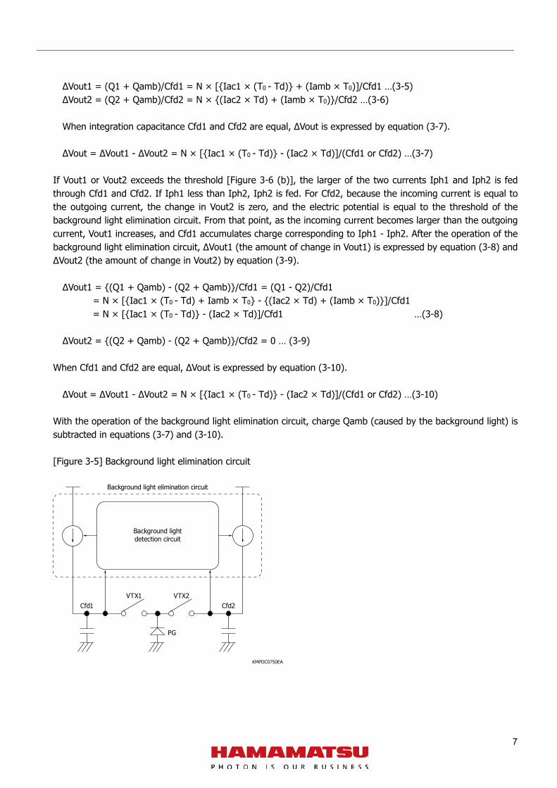
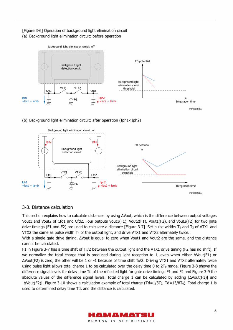
The distance image sensors S15452/S15453/S15454-01WT are equipped with a background light elimination circuit [Figure 3-5] that suppresses saturation of output voltage when background light is incident. Figure 3-6 shows operation of the background light elimination circuit. When either integration capacitor Cfd1 or Cfd2 approaches saturation, the same amount of current flows to both Cfd1 and Cfd2 in the direction that reduces the integration charge. In this case, the difference value between Vout1 and Vout2 will not change, so it will have no effect on distance measurement. The background light elimination circuit automatically functions when the output voltage approaches saturation, and ON/OFF cannot be controlled. We denote the current caused by the signal light flowing through Cfd1 and Cfd2 as Iac1 and Iac2 and the current caused by background light as Iamb. The charges caused by Iac1, Iac2, and Iamb are not distinguished and integrated simultaneously [Figure 3-6]. We denote the current caused by the incident light (signal light + background light) flowing through Cfd1 and Cfd2 as Iph1 and Iph2. If Vout1 and Vout2 do not exceed the threshold [Figure 3-6 (a)], ΔVout1 (the amount of change in Vout1) is expressed by equation (3-5) and ΔVout2 (the amount of change in Vout2) by equation (3-6).
Q1
Td
T0
Q2
Output light
Reflected light
VTX1
VTX2
Background light
VTX1
VTX2
Qamb
Qamb
Signal light only
Vout1 Vout2
Signal light + background light
Q1
Q2∆Vout
Vout1 Vout2
Q1
Q2∆Vout
Qamb Qamb
7
ΔVout1 = (Q1 + Qamb)/Cfd1 = N × [{Iac1 × (T0 - Td)} + (Iamb × T0)]/Cfd1 …(3-5) ΔVout2 = (Q2 + Qamb)/Cfd2 = N × {(Iac2 × Td) + (Iamb × T0)}/Cfd2 …(3-6) When integration capacitance Cfd1 and Cfd2 are equal, ΔVout is expressed by equation (3-7). ΔVout = ΔVout1 - ΔVout2 = N × [{Iac1 × (T0 - Td)} - (Iac2 × Td)]/(Cfd1 or Cfd2) …(3-7)
If Vout1 or Vout2 exceeds the threshold [Figure 3-6 (b)], the larger of the two currents Iph1 and Iph2 is fed through Cfd1 and Cfd2. If Iph1 less than Iph2, Iph2 is fed. For Cfd2, because the incoming current is equal to the outgoing current, the change in Vout2 is zero, and the electric potential is equal to the threshold of the background light elimination circuit. From that point, as the incoming current becomes larger than the outgoing current, Vout1 increases, and Cfd1 accumulates charge corresponding to Iph1 - Iph2. After the operation of the background light elimination circuit, ΔVout1 (the amount of change in Vout1) is expressed by equation (3-8) and ΔVout2 (the amount of change in Vout2) by equation (3-9).
ΔVout1 = {(Q1 + Qamb) - (Q2 + Qamb)}/Cfd1 = (Q1 - Q2)/Cfd1
= N × [{Iac1 × (T0 - Td) + Iamb × T0} - {(Iac2 × Td) + (Iamb × T0)}]/Cfd1 = N × [{Iac1 × (T0 - Td)} - (Iac2 × Td)]/Cfd1 …(3-8)
ΔVout2 = {(Q2 + Qamb) - (Q2 + Qamb)}/Cfd2 = 0 … (3-9)
When Cfd1 and Cfd2 are equal, ΔVout is expressed by equation (3-10).
ΔVout = ΔVout1 - ΔVout2 = N × [{Iac1 × (T0 - Td)} - (Iac2 × Td)]/(Cfd1 or Cfd2) …(3-10)
With the operation of the background light elimination circuit, charge Qamb (caused by the background light) is subtracted in equations (3-7) and (3-10). [Figure 3-5] Background light elimination circuit
KMPDC0750EA
Background light elimination circuit
Background lightdetection circuit
Cfd1VTX1 VTX2
PG
Cfd2
8
[Figure 3-6] Operation of background light elimination circuit (a) Background light elimination circuit: before operation
KMPDC0751EA
(b) Background light elimination circuit: after operation (Iph1<Iph2)
KMPDC0752EA
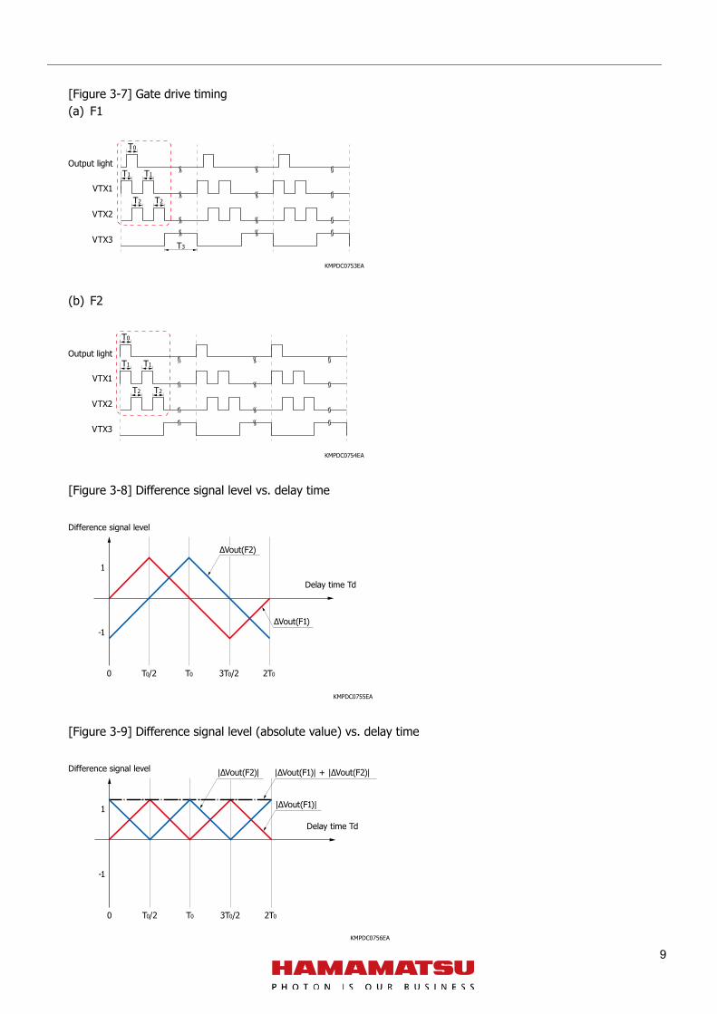
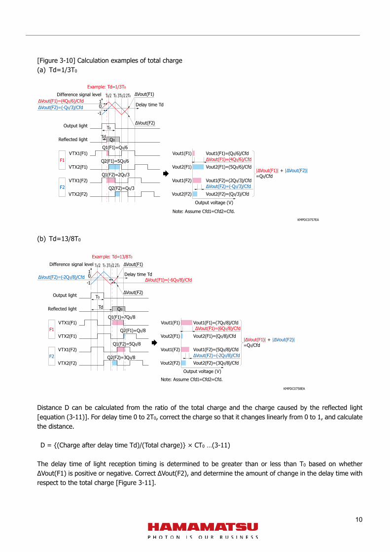
3-3. Distance calculation This section explains how to calculate distances by using ΔVout, which is the difference between output voltages Vout1 and Vout2 of Cfd1 and Cfd2. Four outputs Vout1(F1), Vout2(F1), Vout1(F2), and Vout2(F2) for two gate drive timings (F1 and F2) are used to calculate a distance [Figure 3-7]. Set pulse widths T1 and T2 of VTX1 and VTX2 the same as pulse width T0 of the output light, and drive VTX1 and VTX2 alternately twice. With a single gate drive timing, ΔVout is equal to zero when Vout1 and Vout2 are the same, and the distance cannot be calculated. F1 in Figure 3-7 has a time shift of T0/2 between the output light and the VTX1 drive timing (F2 has no shift). If we normalize the total charge that is produced during light reception to 1, even when either ΔVout(F1) or ΔVout(F2) is zero, the other will be 1 or -1 because of time shift T0/2. Driving VTX1 and VTX2 alternately twice using pulse light allows total charge 1 to be calculated over the delay time 0 to 2T0 range. Figure 3-8 shows the difference signal levels for delay time Td of the reflected light for gate drive timings F1 and F2 and Figure 3-9 the absolute values of the difference signal levels. Total charge 1 can be calculated by adding |ΔVout(F1)| and |ΔVout(F2)|. Figure 3-10 shows a calculation example of total charge (Td=1/3T0, Td=13/8T0). Total charge 1 is used to determined delay time Td, and the distance is calculated.
Background light elimination circuit: off
Cfd1VTX1 VTX2
PG
Cfd2
lph2=lac2 + lamb
lph1=lac1 + lamb Integration time
FD potential
Background lightelimination circuit
threshold
Background lightdetection circuit
Background light elimination circuit: on
Cfd1VTX1 VTX2
PG
Cfd2
lph2=lac2 + lamb
lph1=lac1 + lamb Integration time
FD potential
Background lightelimination circuit
threshold
lph2lph2 lph2lph2
Background lightdetection circuit
9
[Figure 3-7] Gate drive timing (a) F1
KMPDC0753EA
(b) F2
KMPDC0754EA
[Figure 3-8] Difference signal level vs. delay time
KMPDC0755EA
[Figure 3-9] Difference signal level (absolute value) vs. delay time
KMPDC0756EA
Output light
VTX1
VTX2
VTX3
T2
T1
T0
T1
T2
T3
Output light
VTX1
VTX2
VTX3
T2
T1
T0
T1
T2
Difference signal level
Delay time Td
0
-1
1
T0/2 T0 3T0/2 2T0
∆Vout(F1)
∆Vout(F2)
Difference signal level
Delay time Td
0
-1
1
T0/2 T0 3T0/2 2T0
|∆Vout(F2)|
|∆Vout(F1)|
|∆Vout(F1)| + |∆Vout(F2)|
10
[Figure 3-10] Calculation examples of total charge (a) Td=1/3T0
KMPDC0757EA
(b) Td=13/8T0
KMPDC0758EA
Distance D can be calculated from the ratio of the total charge and the charge caused by the reflected light [equation (3-11)]. For delay time 0 to 2T0, correct the charge so that it changes linearly from 0 to 1, and calculate the distance. D = {(Charge after delay time Td)/(Total charge)} × CT0 …(3-11)
The delay time of light reception timing is determined to be greater than or less than T0 based on whether ΔVout(F1) is positive or negative. Correct ΔVout(F2), and determine the amount of change in the delay time with respect to the total charge [Figure 3-11].
Difference signal level
Output light
Reflected light
VTX1(F1)
VTX2(F1)
VTX1(F2)
VTX2(F2)
Delay time Td
-101
Example: Td=1/3T0
∆Vout(F2)T0
Q0
Q1(F1)=Q0/6
Q2(F1)=5Q0/6
Q1(F2)=2Q0/3
Q2(F2)=Q0/3
∆Vout(F1)∆Vout(F1)=(4Q0/6)/Cfd∆Vout(F2)=(-Q0/3)/Cfd
∆Vout(F1)=(4Q0/6)/CfdVout1(F1)
Vout2(F1)
Vout1(F2)
Vout2(F2)
Vout1(F1)=(Q0/6)/Cfd
Vout2(F1)=(5Q0/6)/Cfd
Vout1(F2)=(2Q0/3)/Cfd
Vout2(F2)=(Q0/3)/Cfd∆Vout(F2)=(-Q0/3)/Cfd
Output voltage (V)
Note: Assume Cfd1=Cfd2=Cfd.
|∆Vout(F1)| + |∆Vout(F2)|=Q0/Cfd
F1
F2
Td
Difference signal level
Output light
Reflected light
VTX1(F1)
VTX2(F1)
VTX1(F2)
VTX2(F2)
Delay time Td
-101
Example: Td=13/8T0
Td
∆Vout(F2)T0
Q0
Q1(F1)=7Q0/8
Q2(F1)=Q0/8
Q1(F2)=5Q0/8
Q2(F2)=3Q0/8
∆Vout(F1)
∆Vout(F2)=(-2Q0/8)/Cfd ∆Vout(F1)=(-6Q0/8)/Cfd
∆Vout(F1)=(6Q0/8)/CfdVout1(F1)
Vout2(F1)
Vout1(F2)
Vout2(F2)
Vout1(F1)=(7Q0/8)/Cfd
Vout2(F1)=(Q0/8)/Cfd
Vout1(F2)=(5Q0/8)/Cfd
Vout2(F2)=(3Q0/8)/Cfd∆Vout(F2)=(-2Q0/8)/Cfd
Note: Assume Cfd1=Cfd2=Cfd.
|∆Vout(F1)| + |∆Vout(F2)|=Q0/Cfd
F1
F2
Output voltage (V)
11
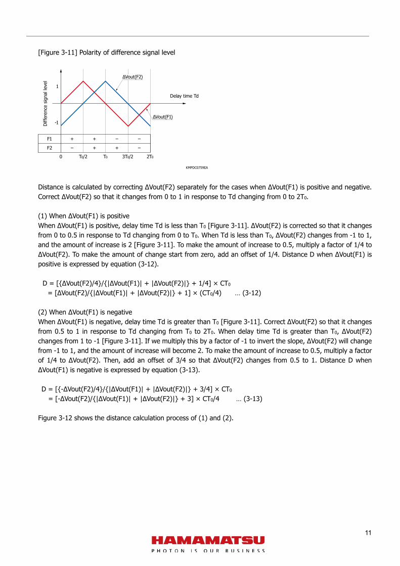
[Figure 3-11] Polarity of difference signal level
KMPDC0759EA
Distance is calculated by correcting ΔVout(F2) separately for the cases when ΔVout(F1) is positive and negative. Correct ΔVout(F2) so that it changes from 0 to 1 in response to Td changing from 0 to 2T0. (1) When ΔVout(F1) is positive When ΔVout(F1) is positive, delay time Td is less than T0 [Figure 3-11]. ΔVout(F2) is corrected so that it changes from 0 to 0.5 in response to Td changing from 0 to T0. When Td is less than T0, ΔVout(F2) changes from -1 to 1, and the amount of increase is 2 [Figure 3-11]. To make the amount of increase to 0.5, multiply a factor of 1/4 to ΔVout(F2). To make the amount of change start from zero, add an offset of 1/4. Distance D when ΔVout(F1) is positive is expressed by equation (3-12). D = [{ΔVout(F2)/4}/{|ΔVout(F1)| + |ΔVout(F2)|} + 1/4] × CT0
= [ΔVout(F2)/{|ΔVout(F1)| + |ΔVout(F2)|} + 1] × (CT0/4) … (3-12)
(2) When ΔVout(F1) is negative When ΔVout(F1) is negative, delay time Td is greater than T0 [Figure 3-11]. Correct ΔVout(F2) so that it changes from 0.5 to 1 in response to Td changing from T0 to 2T0. When delay time Td is greater than T0, ΔVout(F2) changes from 1 to -1 [Figure 3-11]. If we multiply this by a factor of -1 to invert the slope, ΔVout(F2) will change from -1 to 1, and the amount of increase will become 2. To make the amount of increase to 0.5, multiply a factor of 1/4 to ΔVout(F2). Then, add an offset of 3/4 so that ΔVout(F2) changes from 0.5 to 1. Distance D when ΔVout(F1) is negative is expressed by equation (3-13).
D = [{-ΔVout(F2)/4}/{|ΔVout(F1)| + |ΔVout(F2)|} + 3/4] × CT0
= [-ΔVout(F2)/{|ΔVout(F1)| + |ΔVout(F2)|} + 3] × CT0/4 … (3-13)
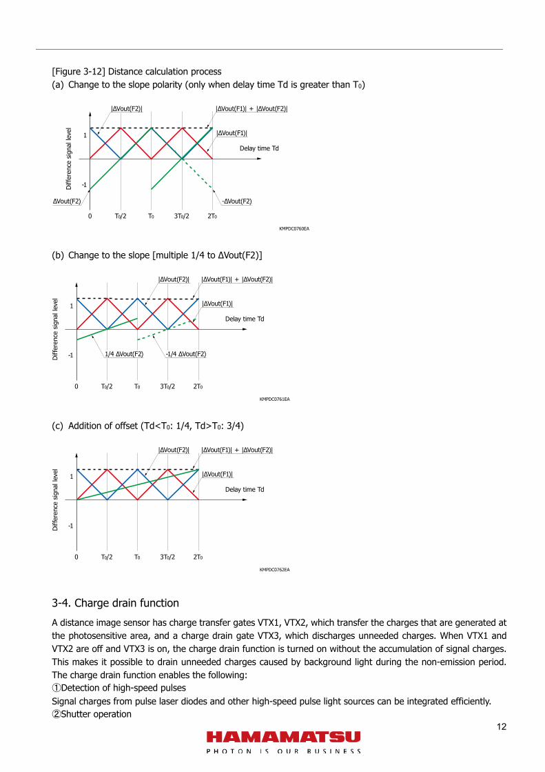
Figure 3-12 shows the distance calculation process of (1) and (2).
Diffe
renc
esig
nall
evel
Delay time Td
0
-1
1
T0/2 T0 3T0/2 2T0
∆Vout(F1)
∆Vout(F2)
+
−
+
+
−
+
−
−
F1
F2
12
[Figure 3-12] Distance calculation process (a) Change to the slope polarity (only when delay time Td is greater than T0)
KMPDC0760EA
(b) Change to the slope [multiple 1/4 to ΔVout(F2)]
KMPDC0761EA
(c) Addition of offset (Td<T0: 1/4, Td>T0: 3/4)
KMPDC0762EA
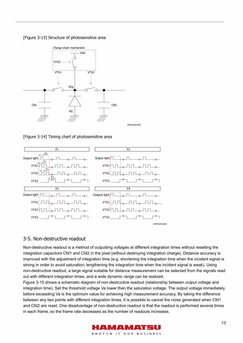
3-4. Charge drain function A distance image sensor has charge transfer gates VTX1, VTX2, which transfer the charges that are generated at the photosensitive area, and a charge drain gate VTX3, which discharges unneeded charges. When VTX1 and VTX2 are off and VTX3 is on, the charge drain function is turned on without the accumulation of signal charges. This makes it possible to drain unneeded charges caused by background light during the non-emission period. The charge drain function enables the following: ①Detection of high-speed pulses Signal charges from pulse laser diodes and other high-speed pulse light sources can be integrated efficiently. ②Shutter operation
Diffe
renc
esig
nall
evel
Delay time Td
0
-1
1
T0/2 T0 3T0/2 2T0
|∆Vout(F2)|
|∆Vout(F1)|
-∆Vout(F2)∆Vout(F2)
|∆Vout(F1)| + |∆Vout(F2)|
Diffe
renc
esig
nall
evel
Delay time Td
0
-1
1
T0/2 T0 3T0/2 2T0
|∆Vout(F2)|
-1/4 ∆Vout(F2)1/4 ∆Vout(F2)
|∆Vout(F1)|
|∆Vout(F1)| + |∆Vout(F2)|
Diffe
renc
esig
nall
evel
Delay time Td
0
-1
1
T0/2 T0 3T0/2 2T0
|∆Vout(F2)|
|∆Vout(F1)|
|∆Vout(F1)| + |∆Vout(F2)|
13
[Figure 3-13] Structure of photosensitive area
KMPDC0635EA
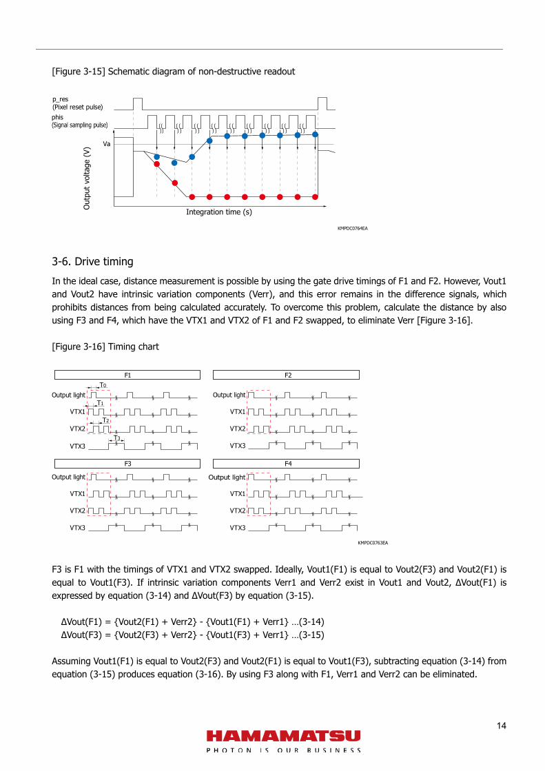
[Figure 3-14] Timing chart of photosensitive area
KMPDC0763EA
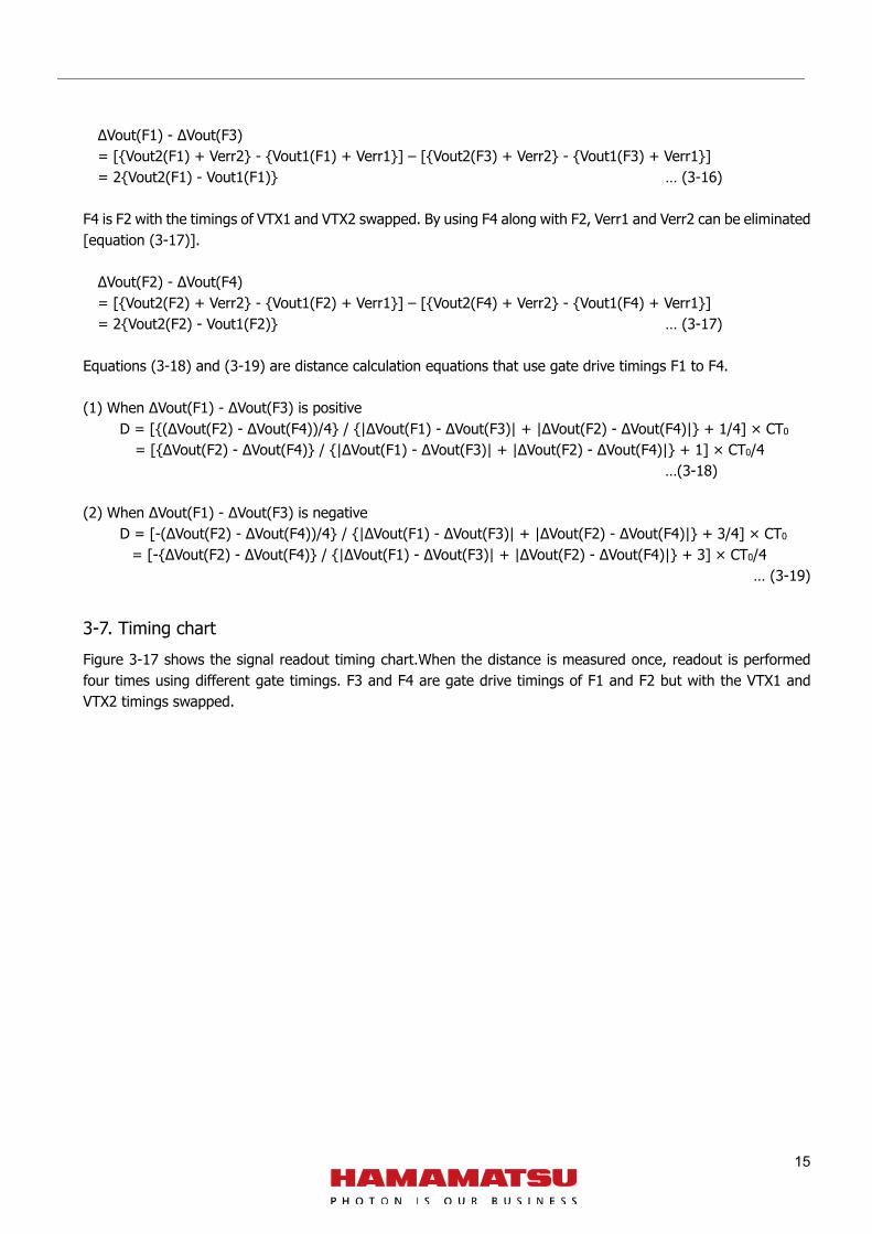
3-5. Non-destructive readout Non-destructive readout is a method of outputting voltages at different integration times without resetting the integration capacitors Cfd1 and Cfd2 in the pixel (without destroying integration charge). Distance accuracy is improved with the adjustment of integration time (e.g. shortening the integration time when the incident signal is strong in order to avoid saturation; lengthening the integration time when the incident signal is weak). Using non-destructive readout, a large signal suitable for distance measurement can be selected from the signals read out with different integration times, and a wide dynamic range can be realized. Figure 3-15 shows a schematic diagram of non-destructive readout (relationship between output voltage and integration time). Set the threshold voltage Va lower than the saturation voltage. The output voltage immediately before exceeding Va is the optimum value for achieving high measurement accuracy. By taking the difference between any two points with different integration times, it is possible to cancel the noise generated when Cfd1 and Cfd2 are reset. One disadvantage of non-destructive readout is that the readout is performed several times in each frame, so the frame rate decreases as the number of readouts increases.
VTX1
VTX3
VTX2
Vdd
Vpg
Cfd1 Cfd2
PG
Charge drain mechanism
Output light
VTX1
VTX2
VTX3 VTX3
VTX2
VTX1
F1T0
T1
T2
T3
Output light
VTX3
VTX2
VTX1
VTX3
VTX2
VTX1
F2
F3 F4
14
[Figure 3-15] Schematic diagram of non-destructive readout
KMPDC0764EA
3-6. Drive timing In the ideal case, distance measurement is possible by using the gate drive timings of F1 and F2. However, Vout1 and Vout2 have intrinsic variation components (Verr), and this error remains in the difference signals, which prohibits distances from being calculated accurately. To overcome this problem, calculate the distance by also using F3 and F4, which have the VTX1 and VTX2 of F1 and F2 swapped, to eliminate Verr [Figure 3-16]. [Figure 3-16] Timing chart
KMPDC0763EA
F3 is F1 with the timings of VTX1 and VTX2 swapped. Ideally, Vout1(F1) is equal to Vout2(F3) and Vout2(F1) is equal to Vout1(F3). If intrinsic variation components Verr1 and Verr2 exist in Vout1 and Vout2, ΔVout(F1) is expressed by equation (3-14) and ΔVout(F3) by equation (3-15). ΔVout(F1) = {Vout2(F1) + Verr2} - {Vout1(F1) + Verr1} …(3-14) ΔVout(F3) = {Vout2(F3) + Verr2} - {Vout1(F3) + Verr1} …(3-15)
Assuming Vout1(F1) is equal to Vout2(F3) and Vout2(F1) is equal to Vout1(F3), subtracting equation (3-14) from equation (3-15) produces equation (3-16). By using F3 along with F1, Verr1 and Verr2 can be eliminated.
Integration time (s)Outp
ut v
olta
ge (V
)p_res(Pixel reset pulse)phis
Output light
VTX1
VTX2
VTX3 VTX3
VTX2
VTX1
F1T0
T1
T2
T3
Output light
VTX3
VTX2
VTX1
VTX3
VTX2
VTX1
F2
F3 F4
15
ΔVout(F1) - ΔVout(F3) = [{Vout2(F1) + Verr2} - {Vout1(F1) + Verr1}] – [{Vout2(F3) + Verr2} - {Vout1(F3) + Verr1}] = 2{Vout2(F1) - Vout1(F1)} … (3-16)
F4 is F2 with the timings of VTX1 and VTX2 swapped. By using F4 along with F2, Verr1 and Verr2 can be eliminated [equation (3-17)].
ΔVout(F2) - ΔVout(F4) = [{Vout2(F2) + Verr2} - {Vout1(F2) + Verr1}] – [{Vout2(F4) + Verr2} - {Vout1(F4) + Verr1}] = 2{Vout2(F2) - Vout1(F2)} … (3-17)
Equations (3-18) and (3-19) are distance calculation equations that use gate drive timings F1 to F4.
(1) When ΔVout(F1) - ΔVout(F3) is positive D = [{(ΔVout(F2) - ΔVout(F4))/4} / {|ΔVout(F1) - ΔVout(F3)| + |ΔVout(F2) - ΔVout(F4)|} + 1/4] × CT0
= [{ΔVout(F2) - ΔVout(F4)} / {|ΔVout(F1) - ΔVout(F3)| + |ΔVout(F2) - ΔVout(F4)|} + 1] × CT0/4 …(3-18)
(2) When ΔVout(F1) - ΔVout(F3) is negative
D = [-(ΔVout(F2) - ΔVout(F4))/4} / {|ΔVout(F1) - ΔVout(F3)| + |ΔVout(F2) - ΔVout(F4)|} + 3/4] × CT0
= [-{ΔVout(F2) - ΔVout(F4)} / {|ΔVout(F1) - ΔVout(F3)| + |ΔVout(F2) - ΔVout(F4)|} + 3] × CT0/4 … (3-19)
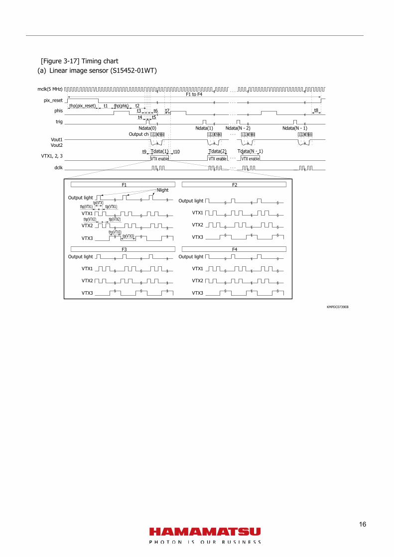
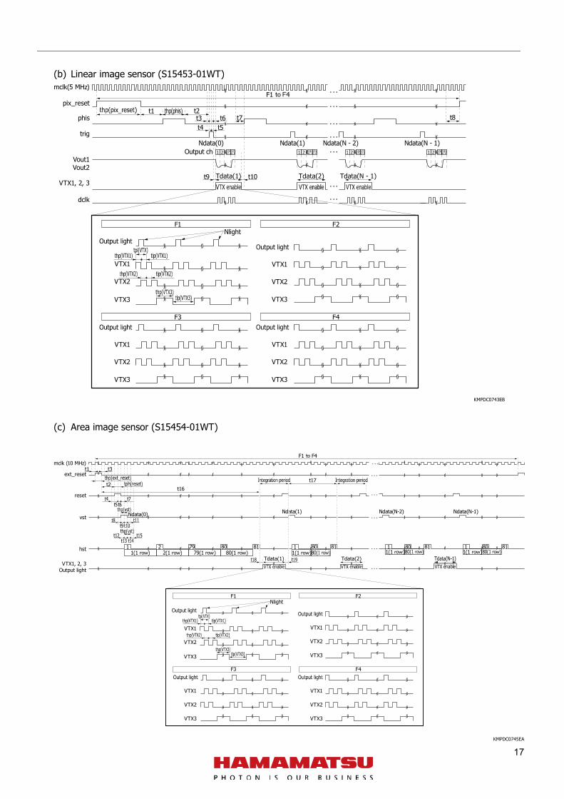
3-7. Timing chart Figure 3-17 shows the signal readout timing chart.When the distance is measured once, readout is performed four times using different gate timings. F3 and F4 are gate drive timings of F1 and F2 but with the VTX1 and VTX2 timings swapped.
16
[Figure 3-17] Timing chart (a) Linear image sensor (S15452-01WT)
KMPDC0739EB
mclk(5 MHz)
pix_reset
trig
Vout1Vout2
dclk
VTX1, 2, 3
phis
1 2 1 2 1 2 1 2
Ndata(0)
Tdata(1) Tdata(2) Tdata(N - 1)
Ndata(1)
F1 to F4
Ndata(N - 2) Ndata(N - 1)
Output light
VTX1
VTX2
VTX3
Output light
VTX3
VTX2
VTX1
NlightF1 F2
F3 F4Output light
VTX3
VTX2
VTX1
Output light
VTX3
VTX2
VTX1
⸱ ⸱ ⸱
⸱ ⸱ ⸱
⸱ ⸱ ⸱
⸱ ⸱ ⸱
⸱ ⸱ ⸱
⸱ ⸱ ⸱
⸱ ⸱ ⸱
t1 t2t3 t6t4 t5
t7
Output ch
t9
t8
17
(b) Linear image sensor (S15453-01WT)
KMPDC0743EB
(c) Area image sensor (S15454-01WT)
KMPDC0745EA
mclk(5 MHz)
pix_reset
trig
Vout1Vout2
dclk
VTX1, 2, 3
phis
1 2 1 2 1 2 1 2
Ndata(0)
Tdata(1) Tdata(2) Tdata(N - 1)
Ndata(1)
F1 to F4
Ndata(N - 2) Ndata(N - 1)
VTX1
VTX2
VTX3 VTX3
VTX2
VTX1
NlightF1 F2
F3 F4
・・・
・・・
・・・
・・・
・・・
・・・
VTX3
VTX2
VTX1
VTX3
VTX2
VTX1
・・・
t1 t2t3 t6t4 t5
t7
Output ch
t9
t8
mclk (10 MHz)
ext_reset
reset
VTX1, 2, 3Output light
hst
vst
F1 to F4
1(1 row)80 81
80(1 row)81
79(1 row)80
2(1 row)79
1(1 row)21
Ndata(1)
1
Tdata(1) Tdata(2)
Ndata(N-2) Ndata(N-1)
1(1 row)80 811
1(1 row)80 811
・・・
・・・
・・・
t1 t3
t2t16
t17・・・
・・・
・・・
VTX1
VTX2
VTX3 VTX3
VTX2
VTX1
NlightF1 F2
F3 F4
VTX3
VTX2
VTX1
VTX3
VTX2
VTX1
Ndata(0)
18
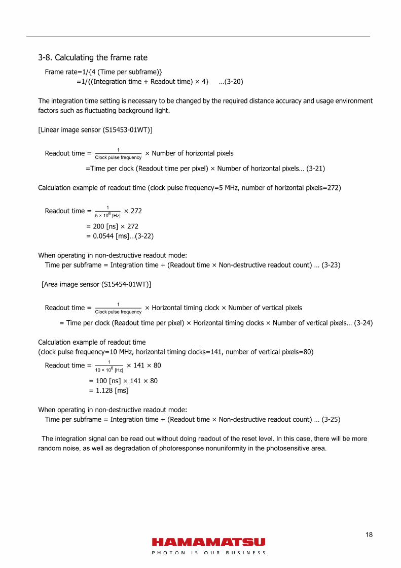
3-8. Calculating the frame rate Frame rate=1/{4 (Time per subframe)}
=1/{(Integration time + Readout time) × 4} …(3-20)
The integration time setting is necessary to be changed by the required distance accuracy and usage environment factors such as fluctuating background light. [Linear image sensor (S15453-01WT)]
Readout time = 1Clock pulse frequency
× Number of horizontal pixels
=Time per clock (Readout time per pixel) × Number of horizontal pixels… (3-21)
Calculation example of readout time (clock pulse frequency=5 MHz, number of horizontal pixels=272)
Readout time = 15 × 106 [Hz]
× 272
= 200 [ns] × 272 = 0.0544 [ms]…(3-22)
When operating in non-destructive readout mode:
Time per subframe = Integration time + (Readout time × Non-destructive readout count) … (3-23) [Area image sensor (S15454-01WT)]
Readout time = 1Clock pulse frequency
× Horizontal timing clock × Number of vertical pixels
= Time per clock (Readout time per pixel) × Horizontal timing clocks × Number of vertical pixels… (3-24)
Calculation example of readout time (clock pulse frequency=10 MHz, horizontal timing clocks=141, number of vertical pixels=80)
Readout time = 110 × 106 [Hz]
× 141 × 80
= 100 [ns] × 141 × 80 = 1.128 [ms]
When operating in non-destructive readout mode: Time per subframe = Integration time + (Readout time × Non-destructive readout count) … (3-25)
The integration signal can be read out without doing readout of the reset level. In this case, there will be more
random noise, as well as degradation of photoresponse nonuniformity in the photosensitive area.
19
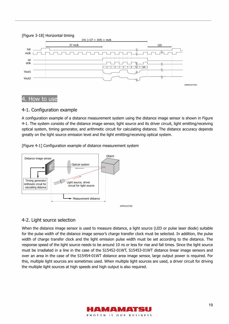
[Figure 3-18] Horizontal timing
KMPDC0747EC
4. How to use
4-1. Configuration example A configuration example of a distance measurement system using the distance image sensor is shown in Figure 4-1. The system consists of the distance image sensor, light source and its driver circuit, light emitting/receiving optical system, timing generator, and arithmetic circuit for calculating distance. The distance accuracy depends greatly on the light source emission level and the light emitting/receiving optical system. [Figure 4-1] Configuration example of distance measurement system
KMPDC0473EC
4-2. Light source selection When the distance image sensor is used to measure distance, a light source (LED or pulse laser diode) suitable for the pulse width of the distance image sensor’s charge transfer clock must be selected. In addition, the pulse width of charge transfer clock and the light emission pulse width must be set according to the distance. The response speed of the light source needs to be around 10 ns or less for rise and fall times. Since the light source must be irradiated in a line in the case of the S15452-01WT, S15453-01WT distance linear image sensors and over an area in the case of the S15454-01WT distance area image sensor, large output power is required. For this, multiple light sources are sometimes used. When multiple light sources are used, a driver circuit for driving the multiple light sources at high speeds and high output is also required.
mclk
dclk
Vout1
Vout2
oe
hst
1 2 3 4 104
37 mclk t20
141 (=37 + 104) × mclk
Light source, drivercircuit for light source
Object
Optical system
Measurement distance
Distance image sensor
Timing generator
20
5. Calibration After the distance image sensor and the light source are combined, distance calibration is necessary. The reasons why calibration is necessary are shown below. [Reasons why calibration is necessary] • Delay in the light emission timing • Delay in the wiring between the sensor and light source • Shape of the light emission pulse of light source • Peripheral circuits
The following shows an example of the calibration method. Distance D is given by equations (5-1)(5-2).
(1) When Td ≤ T0
D=α( VoutB|VoutA| + |VoutB| +1) × CT0
4 - Dofs … (5-1)
(2) When T0 < Td ≤ 2T0
D=α( -VoutB|VoutA| + |VoutB| +3) × CT0
4 - Dofs … (5-2)
α: slope c: speed of light T0: light emission pulse width Dofs: Distance offset
You need to set the light emission timing delay (Light_pulse_delay), distance offset (Dofs), and slope (α).
Setting the light emission timing delay, distance offset, and Dofs The calculated distance is shifted by changing the light emission timing delay and distance offset so that the calculated distance matches the actual distance.
Setting the slope α Select two points in the linear range of distance, and calculate α to match the ideal line [Figure 5-1].
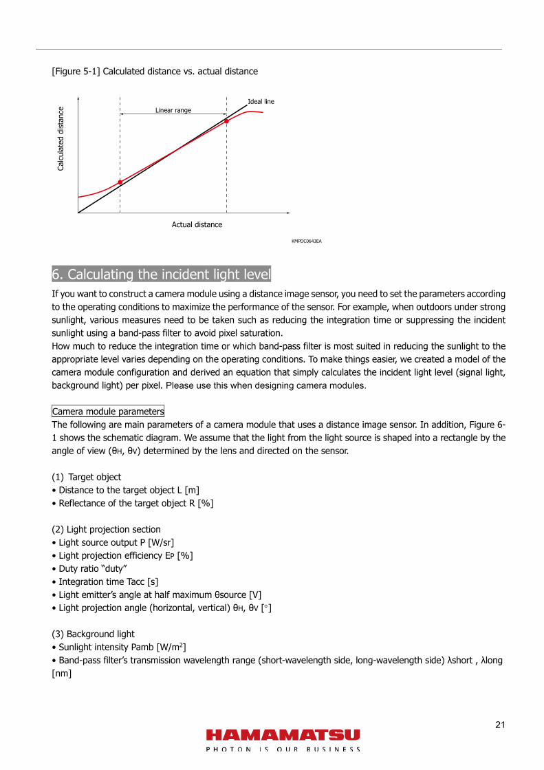
21
[Figure 5-1] Calculated distance vs. actual distance
KMPDC0643EA
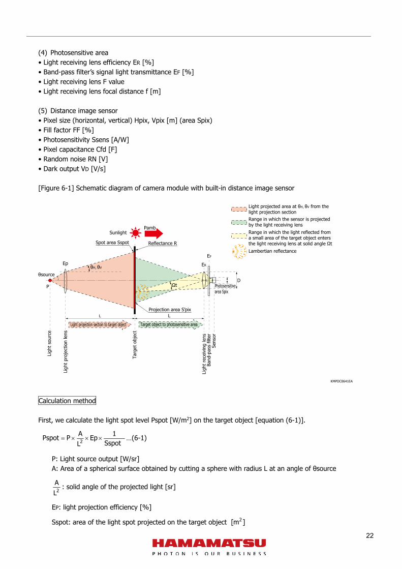
6. Calculating the incident light level If you want to construct a camera module using a distance image sensor, you need to set the parameters according to the operating conditions to maximize the performance of the sensor. For example, when outdoors under strong sunlight, various measures need to be taken such as reducing the integration time or suppressing the incident sunlight using a band-pass filter to avoid pixel saturation. How much to reduce the integration time or which band-pass filter is most suited in reducing the sunlight to the appropriate level varies depending on the operating conditions. To make things easier, we created a model of the camera module configuration and derived an equation that simply calculates the incident light level (signal light, background light) per pixel. Please use this when designing camera modules. Camera module parameters The following are main parameters of a camera module that uses a distance image sensor. In addition, Figure 6-1 shows the schematic diagram. We assume that the light from the light source is shaped into a rectangle by the angle of view (θH, θV) determined by the lens and directed on the sensor. (1) Target object • Distance to the target object L [m] • Reflectance of the target object R [%]
(2) Light projection section • Light source output P [W/sr] • Light projection efficiency EP [%] • Duty ratio “duty” • Integration time Tacc [s] • Light emitter’s angle at half maximum θsource [V] • Light projection angle (horizontal, vertical) θH, θV [] (3) Background light • Sunlight intensity Pamb [W/m2] • Band-pass filter’s transmission wavelength range (short-wavelength side, long-wavelength side) λshort , λlong [nm]
Calcu
late
d di
stan
ce
Actual distance
Linear rangeIdeal line
22
(4) Photosensitive area • Light receiving lens efficiency ER [%] • Band-pass filter’s signal light transmittance EF [%] • Light receiving lens F value • Light receiving lens focal distance f [m] (5) Distance image sensor • Pixel size (horizontal, vertical) Hpix, Vpix [m] (area Spix) • Fill factor FF [%] • Photosensitivity Ssens [A/W] • Pixel capacitance Cfd [F] • Random noise RN [V] • Dark output VD [V/s] [Figure 6-1] Schematic diagram of camera module with built-in distance image sensor
KMPDC0641EA
Calculation method First, we calculate the light spot level Pspot [W/m2] on the target object [equation (6-1)].
Sspot1Ep
LAPPspot 2 …(6-1)
P: Light source output [W/sr] A: Area of a spherical surface obtained by cutting a sphere with radius L at an angle of θsource
2LA : solid angle of the projected light [sr]
EP: light projection efficiency [%]
Sspot: area of the light spot projected on the target object ]m[ 2
Light projected area at θH, θV from thelight projection sectionRange in which the sensor is projectedby the light receiving lensRange in which the light reflected froma small area of the target object entersthe light receiving lens at solid angle ΩtLambertian reflectance
Photosensitivearea Spix
EF
EREp
Target object to photosensitive areaLight projection section to target object
L L
Pamb
θH, θV
Ωt
θsource
P
Sunlight
Spot area Sspot Reflectance R
Projection area S’pix
23
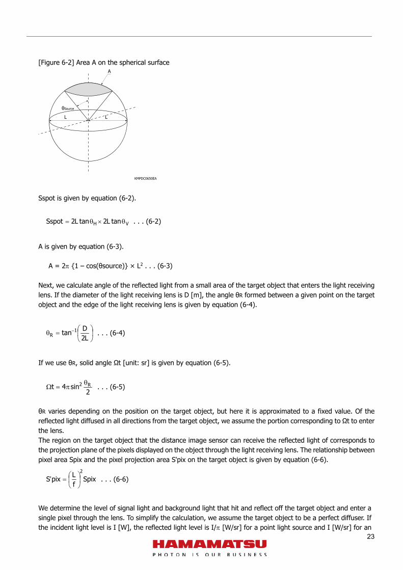
[Figure 6-2] Area A on the spherical surface
KMPDC0650EA
Sspot is given by equation (6-2).
VH tanL2tanL2Sspot . . . (6-2)
A is given by equation (6-3).
A = 2 {1 – cos(θsource)} × L2 . . . (6-3)
Next, we calculate angle of the reflected light from a small area of the target object that enters the light receiving lens. If the diameter of the light receiving lens is D [m], the angle θR formed between a given point on the target object and the edge of the light receiving lens is given by equation (6-4).
L2Dtan 1
R . . . (6-4)
If we use θR, solid angle Ωt [unit: sr] is given by equation (6-5).
2sin4t R2 . . . (6-5)
θR varies depending on the position on the target object, but here it is approximated to a fixed value. Of the reflected light diffused in all directions from the target object, we assume the portion corresponding to Ωt to enter the lens. The region on the target object that the distance image sensor can receive the reflected light of corresponds to the projection plane of the pixels displayed on the object through the light receiving lens. The relationship between pixel area Spix and the pixel projection area S'pix on the target object is given by equation (6-6).
SpixfLpixS
2
. . . (6-6)
We determine the level of signal light and background light that hit and reflect off the target object and enter a single pixel through the lens. To simplify the calculation, we assume the target object to be a perfect diffuser. If the incident light level is I [W], the reflected light level is I/ [W/sr] for a point light source and I [W/sr] for an
L L
A
θSource
24
extremely wide surface light source such as sunlight. The signal light level Ppix [W] entering a single pixel is given by equation (6-7).
FF)sig(EEpix'St1RPspotPpix FR
. . . (6-7)
The background light level Ppix(amb) [W] entering a single pixel is given by equation (6-8).
FF)amb(EEpix'St1RPamp)amb(Ppix FR . . . (6-8)
EF(sig): band-pass filter transmittance for signal light EF(amb): band-pass filter transmittance for background light
Output voltage Vpix [V] generated from the signal light is given by equation (6-9).
CfdSsensdutyTaccPpixVpix . . . (6-9)
Tacc: integration time [s] duty: duty ratio Ssens: photosensitivity [A/W] Cfd: pixel capacitance [F]
Output voltage Vpix(amb) [V] generated from the background light is given by equation (6-10). Because background light is incident at the two gate drive timings, we double Vpix(amb).
Vpix(amb) = Ppix(amb) × Tacc × duty × (Ssens/Cfd) × 2 …(6-10)
Distance accuracy Using the levels of signal light and background light entering a single pixel determined above, we calculate the distance accuracy of the camera module. Photocurrent Ipix [A] per pixel generated by the signal light is given by equation (6-11).
Ipix = Ppix × Ssens . . . (6-11)
The number of electrons Qpix [e-] per pixel generated by the signal light is given by equation (6-12). Qpix = Ipix × Tacc × duty/e . . . (6-12)
= Ppix × Ssens × Tacc × duty/e
e: quantum of electricity=1.602 × 10⁻¹⁹ [C]
The number of electrons Qpix(amb) [e-] per pixel generated by the background light is given by equation (6-13).
Qpix(amb) = Ppix(amb) × Ssens × Tacc ×duty/e × 2 …(6-13)
Next, noise components are described. The amplitudes of light shot noise NL, random noise NR, dark current shot noise ND are given by the following equations [unit: e-].
NL = )amb(QpixQpix . . . (6-14)
25
NR = 2 × RN × Cfd/e . . . (6-15)
RN: random noise [V]
ND = 2×VD×Tacc×Cfd e ⁄ . . . (6-16)
VD: dark output [V]
Total noise N [e-] is given by equation (6-17).
N = 2D
2R
2 NNNL
. . . (6-17)
The S/N is the ratio of the number of signal electrons Qpix to N. Distance accuracy σ [m] is given by equation (6-18).
2cT
QpixN 0 . . . (6-18)
c: speed of light T0: light emission pulse width
Increasing the incident signal level helps to improve the distance accuracy. As the temperature rises, dark current shot noise increases and distance accuracy worsens, so it is necessary to consider the heat dissipation design of the distance image sensor.
7. Evaluation kit Figure 8-1 shows a configuration example using the evaluation kit for the distance image sensor. This evaluation kit can generate sensor drive timing with an FPGA and sensor bias voltage with a DAC-IC, perform A/D conversion on the sensor output signal, and transfer data to a PC via USB 3.0. This evaluation kit can be driven with only a 5 V power supply. Hamamatsu provides evaluation kits (with LED array and light receiving lens) for the S15452-01WT, S15453-01WT, and S15454-01WT. [Figure 7-1] Configuration example of distance measurement using the evaluation kit
KMPDC0417EC
Target(person, object)
Light source(LED or LD)
PC
USB
Drive pulse
Evaluationkit Irradiation light
Reflected lightDistanceimagesensor
26 Cat. No. KMPD9014E01 Aug. 2020
[Figure 7-2] Evaluation kit examples (a) For linear image sensors
(b) For area image sensor