dke090x answers
TRANSCRIPT
8/13/2019 Dke090x Answers
http://slidepdf.com/reader/full/dke090x-answers 1/22
Answers to Problems
CHAPTER 2
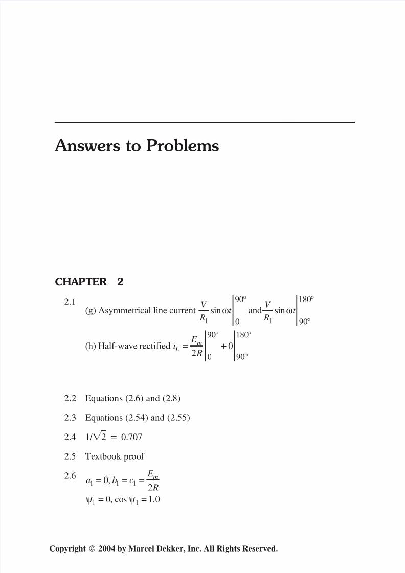
2.1 V
Rt
V
Rt
i E
R L
m
1 10
90
90
180
0
90
90
180
20
s(g) Asymmetrical line current
(h) Half-wave rectified
in sinω ω °
°
°
°
°
°= +
and
2.2 Equations (2.6) and (2.8)
2.3 Equations (2.54) and (2.55)
2.4 1/ 2 0.707
2.5 Textbook proof
2.6a b c
E
R
m1 1 1
1 1
02
0 1 0
= = =
= =
,
, cos .ψ ψ
Copyright 2004 by Marcel Dekker, Inc. All Rights Reserved.

8/13/2019 Dke090x Answers
http://slidepdf.com/reader/full/dke090x-answers 2/22
2.7 E E
E E
RF
avm
Lm
= =
= =
=
2210 1
2233 3
0 48
π .
.
.
V
V
2.8 i t E
Rt t L
m( ) cos cosω π π
ω π
ω = − −
2 4
32
4
154
2.9 I
I
I
I
av
av
m
m
V E m
V
=
=
= =0
/ π π
2.10 I E
Rav
m
= =20 685 0 11
π ( . ) . A
2.11 I L 0.208 A
P 9.83 W
RF 0.668
2.12 I av (supply) 0
I av (load) 0.872 A
(a), (b) Half-wave operation, I av
0.436 A
2.13 See Fig. 2.5.
2.14 is same as in Fig.υ
υ ω θ
π L R
D m
i
E t
x
x
x c
2 5
0
2
. .
sin= +−
2.15 2.15 See Sec. 2.1.2.
2.16 Solution not given here—refer to library texts on applied electronics
2.17i t
E
Rt
E
X t
I I P;
Lm m
c
L R
( ) sin sin( )ω ω ω π π
= + + °
>
0 0
2
90
for some thereefore reduces., PF
2.18 See Sec. 2.3.1.
2.19 c 225.8
Copyright 2004 by Marcel Dekker, Inc. All Rights Reserved.

8/13/2019 Dke090x Answers
http://slidepdf.com/reader/full/dke090x-answers 3/22
2.20 (a) Equation (2.72)
(b) Figure 2.11
(c) Differentiate Eq. (2.72) wrt time and equate to zero
2.21 Section 2.3.1 and Fig. 2.11
2.22 c 212
2.23 c 210.05 (by iteration)
I av 4.83 A
2.24 Section 2.31
c 180 45 4 229
2.25 9.06 A
2.26 When de L / dt 0, e L (t ) 0.5 E m.
2.27 X 210.05
c 225.8
I av 0.764 A
Taking the dc, fundamental, plus second harmonic components of the
voltage
I L = + + =
= =
( . ) ( . ) .
..
0 9
1
2 2 0 36 1 41
1
1 410 71
2
A
Distortion factor
2.29 With positive supply voltage there are positive load and supply currents.
With negative supply voltage the secondary current is zero and the pri-
mary current is the magnetizing current.
2.30 Section 2.3.1 and Fig. 2.10
2.31 QED question
2.32 Section 2.4 and Fig. 2.13
2.33 See Sec. 2.4. Current waveform can be deducted from Fig. 2.13.
CHAPTER 3
3.1 See Sec. 3.1.1.
I s (av) 2.387 A
Copyright 2004 by Marcel Dekker, Inc. All Rights Reserved.

8/13/2019 Dke090x Answers
http://slidepdf.com/reader/full/dke090x-answers 4/22
3.3 At 0, P 50 W.
At 180, P 25 W.
Pest 37.5 W.
DC, even and odd order harmonics.
3.4 I av 0.08 A
3.5 See Sec. 3.1.1.
3.6a
E
R
n
n
n
n
b
nm
n n
= + − −
+ +
− − −−
+ −
2
1 1
1
1 1
1
1 1
πα αcos( ) ( ) cos( ) ( )
nnm E
R
n
n
n
n=
++
− −
−
2
1
1
1
1πα αsin( ) sin( )
At α π
π
== = = =
/ ,
. . .
2
0 295 0 2372
0 161 2 3c E
Rc
E
Rc
E
R
E
R
m m m m
3.7 I E
R
I E
R
E
R
I
I
m
m m
1
1
2
0 296
2 20 354
2
=
= =
.
.
/
peak value
rms value
==
=0 29
0 50 35
2.
..
3.8 Equation (3.7)
3.9 No. The supply current waveform will remain nonsinusoidal.
3.10 105.2
3.11 Section 3.1.1
3.12 Section 3.1.1
3.13 Judging PF from the waveforms could be misleading. Better to undertake
the necessary calculations.
3.14 Use Eqs. (3.4) and (3.10) for the uncompensated distortion factor.
Displacement factor cos1 b1 / c1; so use Eqs. (3.9) and (3.10).
3.15 The diode has no effect at all.
3.16 During thyristor conduction the transformer has little effect on the load
Copyright 2004 by Marcel Dekker, Inc. All Rights Reserved.Copyright 2004 by Marcel Dekker, Inc. All Rights Reserved.
8/13/2019 Dke090x Answers
http://slidepdf.com/reader/full/dke090x-answers 5/22
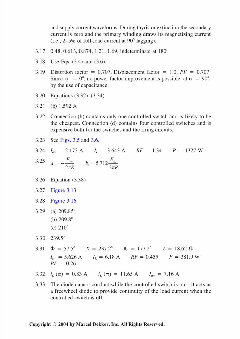
and supply current waveforms. During thyristor extinction the secondary
current is zero and the primary winding draws its magnetizing current
(i.e., 2–5% of full-load current at 90 lagging).
3.17 0.48, 0.613, 0.874, 1.21, 1.69, indeterminate at 180
3.18 Use Eqs. (3.4) and (3.6).
3.19 Distortion factor 0.707. Displacement factor 1.0, PF 0.707.
Since 1 0, no power factor improvement is possible, at 90,
by the use of capacitance.
3.20 Equations (3.32)–(3.34)
3.21 (b) 1.592 A
3.22 Connection (b) contains only one controlled switch and is likely to bethe cheapest. Connection (d) contains four controlled switches and is
expensive both for the switches and the firing circuits.
3.23 See Figs. 3.5 and 3.6.
3.24 I av 2.173 A I L 3.643 A RF 1.34 P 1327 W
3.25 a E
Rb
E
R
m m1 1
25 712
2= − =
π π.
3.26 Equation (3.38)
3.27 Figure 3.13
3.28 Figure 3.16
3.29 (a) 209.85
(b) 209.8
(c) 210
3.30 239.5
3.31 57.5 X 237.2 c 177.2 Z 18.62
I av 5.626 A I L 6.18 A RF 0.455 P 381.9 W
PF 0.26
3.32 i L () 0.83 A i L () 11.65 A I av 7.16 A
3.33 The diode cannot conduct while the controlled switch is on—it acts as
a freewheel diode to provide continuity of the load current when the
controlled switch is off.
Copyright 2004 by Marcel Dekker, Inc. All Rights Reserved.
8/13/2019 Dke090x Answers
http://slidepdf.com/reader/full/dke090x-answers 6/22
3.34 The comments for Problem 3.33 still apply.
3.35 Yes. The supply current waveform is that part of the load current wave-
form (Fig. 3.20) in the intervals t . The fundamental component
of this lags the supply voltage. Hence there is a lagging displacement
angle that can be compensated by a capacitor of appropriate value.
3.36 (a) Figure 3.18, Eq. (3.60)
(b) Figure 3.19
3.37 Equation (3.64)
3.38a I b I d d 1 1 1
2 2
2= − = − =
π α
π α) ψ
πsin c(1+ os
3.39 The waveforms are not a reliable indicator of power factor correction. Itis always better to undertake a calculation.
3.40 Equation (3.65), 1 /2.
3.41Q
E I m d =π
αsin
3.42 This is a QED question.
3.43 a I b I d d 1 1 1
4 4
= − = =π α π α ψ αsin cos
3.44 No solution available.
3.45 Q E I m d = 2
π αsin
3.46 QED question
3.47 QED question
3.48c
E n
n
n
nn
m= + +
++
+ −
−+
+ +2 1 1
1
1 1
1
1 2 22 2π
α α α αcos( )
( )
cos( )
( )
cos cos coss
( )
/ n
n
α
1 2
1 2
−
c 166.6 V c4 41.62 V c6 18.54 V
I av 10.08 A I L 10.24 A P 2097 W RF 0.334
3.49 graphical solution
3.50 graphical solution
Copyright 2004 by Marcel Dekker, Inc. All Rights Reserved.

8/13/2019 Dke090x Answers
http://slidepdf.com/reader/full/dke090x-answers 7/22
CHAPTER 4
4.1 See Eq. (4.5).
4.2 See Eqs. (4.7) and (4.9).
4.3 See Eq. (4.11).
4.4a1 0 b1 c1
0.471 E m
2 R 1 0
Displacement factor cos 1 1.0
4.5 I 0.485
0.687 PF
E m
R I 1 0.471
E m
2 R
Distortion factor
I 1
I
4.6
4.7 1.886 kW
4.8 ia 0 The load current has the waveshape of wave e Da in Fig. 4.6, but
is positive.
4.9 I av
E
R RF s
m( ) . .= =0 276 1 446
4.10 Figure 4.5b to e4.11 See Eq. (4.22).
4.12 See Eqs. (4.25) and (4.11).
4.13 I
I E
R
R
av
I RF 0.477 1.41 compared with 1.446 for R load (Problem 4.9)a
av m
E m
( )( )
supplyload
=
= =
=3
3
2π
4.14 2628 W compared with 2716 W.
Copyright 2004 by Marcel Dekker, Inc. All Rights Reserved.

8/13/2019 Dke090x Answers
http://slidepdf.com/reader/full/dke090x-answers 8/22
4.15a b c
I E
R
av m1 1 10
30 456= = = =
π .
Displacement factor 1.0
4.16
ia ( t )
0.456
[ia ( t ) is in time phase with ea ( t ).]
E m
Rsin t
4.17 I E
R I
E
R
PF
am
am= =
= = ×
0 477 0 322
0 676 0 676
1. .
. , .Distortion factor 11 0 0 676. .=
4.18 a I n n
n
b I n n
nav
nav
= × × =
= × × =
2
3 20
23 2
0
ππ π
ππ π
sin cos ( )
sin sin (
for odd
f for evenn )
4.19 Substitute e L (t ) into the defining equations in the Appendix. Note that
it is a very long and tedious calculation.
4.20 The load current consists of rectangular pulses with conduction period
120.
4.21 9.35 A, 339.5 V
4.22 Figure 4.8, Eq. (4.32)4.23 Equations (4.26) and (4.29) or (4.48)
E aN (rms) varies from E m / 2 at 0 to 0.599 E m at 90.
4.24 () varies almost linearly for 0 60.
4.25 graphical solution
4.26 133.74 V (cf. 196 V), 8.88 A (cf. 9.36 A)
4.27 2627.7 W (unchanged), PF 0.74 (cf 0.676)
4.28 Note in Eq. (4.33) that cos is negative for 90.
4.29 Waveforms similar to Fig. 4.10. Waveform of ia (t ) during overlap is
given in Example 4.8.
CHAPTER 5
5.1 E av 203.85 V E 238.9 V RF 0.611
5.2 (a) 3.24 A
(b) 2.16 A
Copyright 2004 by Marcel Dekker, Inc. All Rights Reserved.

8/13/2019 Dke090x Answers
http://slidepdf.com/reader/full/dke090x-answers 9/22
(c) 1.08 A
(d) 0.289 A
5.3 574 W
5.4 1.838 A at 45
5.5 0 30 60 90 120 150
I av 3.74 3.24 2.16 1.08 0.29 0
I rms 3.8 3.72 2.765 1.73 0.662 0
RF 0.186 0.564 0.8 1.25 2.061 No meaning
5.6 QED question
5.7 P VI 1 cos1 W/phase 1 32.5 574 W
5.8 0 30 60 90 120 150
PF 0.686 0.634 0.5 0.443 0.121 0
The fundamental (supply frequency) component of the supply current
lags the applied phase voltage in time-phase. But the lagging current is
not associated, in any way, with energy storage in a magnetic field.
5.9 The appearance of a current waveform can be deceptive. If the waveform
contains severe discontinuities, it may have a low distortion factor and
therefore a low power factor.
5.10 QED question
5.11 c fR
< − +1 2 3
4 2
cos( )α π
π
5.12 60 90 120
I min / I 5.2% 7.2% 5.66%
5.13 Noenergy storage occurs in the thyristors or in the load resistor. Neverthe-
less, if a 0, there is a component of reactive voltamperes Q 3VI 1sin 1 entering the load. All of the voltamperes entering the capacitors,
Qc 3VI c sin 90, are reactive voltamperes.
Copyright 2004 by Marcel Dekker, Inc. All Rights Reserved.

8/13/2019 Dke090x Answers
http://slidepdf.com/reader/full/dke090x-answers 10/22
5.14 The capacitors have no effect on the average value of the supply current.
5.15 0 30 60 90
I av 3.736 3.235 1.868 0
5.16 0 30 60 90
I s 2.157 1.868 1.078 0
P 1047 785 262 0
PF 0.675 0.585 0.338 0
5.17 Expressions for a1 and b1 are given in Table 5.2
0 30° 60° 90°
1 0 30° 60° 90°
cos 1 1 0.866 .0.5 0
5.18 QED question
5.19 QED question
5.20
0 30 60 90PF L 0.675 0.585 0.338 0
PFR 0.686 0.634 0.5 0.443
5.21 QED question
5.22 QED question
5.23 The degree of power factor improvement is the ratio of PF c [Eq. (5.52)]
to PF [Eq. (5.44)]. 0 30 60 90
PF c / PF 1.355 1.063 1.063 0.83
Note: For 90 the ratio PF c / PF 1.0, implying a reduction of power
factor due to the presence of capacitance.
5.24Q E
X Rm
c
= −
3
2
1 9
2
12
2
2
π
αsin
Copyright 2004 by Marcel Dekker, Inc. All Rights Reserved.

8/13/2019 Dke090x Answers
http://slidepdf.com/reader/full/dke090x-answers 11/22
For uncompensated operation, X c .
Q is zero if C R /9 f sin2 where f frequency.
5.25 The presence of compensating capacitors makes no difference to the
average value of the supply current
5.26 I E
R
m1 2
9
2 2
3
2=
πα πcos distortion factor
5.27 QED question
5.28 QED question
5.29 30° 45° 60° 75°
1.00 1.028 1.155 1.654 E avR
E avL
5.30 The reduction of area due to in Fig. 5.13 is given by
Area = − +
+ °
+ + °∫ e
e eaN
AN CN ( )
230
30
α
α µ
5.31 Evaluation of the integral gives
Area = − +[ ]3
2
E m cos cos( )α α µ
5.32 0° 30° 60° 90°
E av 274.23 241.7 134.11 6
R 6.856 6.043 3.353 meaningless
5.33 Similar in style to Fig. 5.13
5.34 QED question
CHAPTER 6
6.1 The load current waveform (Fig. 6.2 e contains six pulsations in each
supply voltage period. The lowest order alternating current term in the
Fourier series is therefore of sixth harmonic frequency.
Copyright 2004 by Marcel Dekker, Inc. All Rights Reserved.

8/13/2019 Dke090x Answers
http://slidepdf.com/reader/full/dke090x-answers 12/22
6.2 See Figs. 6.1 and 6.2.
I E
R I av
mav load supply= =1 654 0. ( ) ( )
6.3 Equations (6.8)–(6.11)
6.4 I
E
R I av
mav load= =1 827 0. ( ),
6.5 6292 W, 11.25 A
6.6 9.156 A, 6.47 A.
6.7 QED question
6.8 Section 6.1, Eq. (6.11)
6.9 The fundamental component of the load current is in time phase with its
respective phase voltage. Any parallel connected reactor at the supply
point would draw a component of supply current in time quadrature with
the respective phase voltage, without affecting the load current and power.
The net supply current would increase causing reduction of the power
factor.
6.10 See Example 6.6.6.11 The peak amplitude, relative to the maximum dc value, of any voltage
harmonic of order n, for firing angle , in a controlled bridge, is
2 1
1
1
1
2
1 1
0
2 2
E
E n n n n
L
av
n
o
=+
+−
−+ −
=
( ) ( )
cos
( )( )
,
α
αAt
2 2
12
E
E n
L
av
n
o= −( )
6.12 From the relationship of Problem 6.11, with n 6, it is seen that E Ln /
E avo 5.71%.
6.13 See Fig. 6.14.
6.14 See Eqs. (6.16)–(6.19).
6.15 See Eqs. (6.16)–(6.18).
Copyright 2004 by Marcel Dekker, Inc. All Rights Reserved.

8/13/2019 Dke090x Answers
http://slidepdf.com/reader/full/dke090x-answers 13/22
6.16 See the answer to Problem 6.9. Because a1 0, the fundamental compo-
nent of the load current is in time phase with its respective phase voltage.
6.17 I D 57.74 A PRV 339.4 V
6.18 Since a1 0, the displacement factor cos1 1.
== = I
I
1 3
πPF distortion factor (using the expressions in Table 6.1)
6.19 i t E
Rt I
E
Rrmsm m( ) sin ( )ω
πω
πψ = = =
18 18
20
2 1 2 1
6.20 See Eqs. (6.19) and (6.22).
6.21 i t E
Rt t t t a
m( ) sin sin sin sin sinω
π
ω ω ω ω ω = − − + +18 1
55
1
77
1
1111
1
1313
2 t t +
…
I E
R
E
Ra
m m
1
18
21 29
2= =
π.
I I E
Ra
a m
5
1
50 258= = .
I I E
Ra
a m
7
1
70 184= = .
6.22 315.11 V, 19.2
6.23( ) . .
( ) .
a
b
µ
µ
= ° =
= ° =
19 2 0 972
52 0 81
E
E
E
E
av
av
av
av
o
o
6.24 E
E
av
avo
= 0 933.
6.25 Use Eq. (6.29).
6.26 Section 6.3
CHAPTER 7
7.1 See Fig. 7.8.
7.2 (a) 2.81 A, 814.5 W.
(b) 1.621 A, 338 W.
(c) 0.434 A, 49.84 W
Copyright 2004 by Marcel Dekker, Inc. All Rights Reserved.
8/13/2019 Dke090x Answers
http://slidepdf.com/reader/full/dke090x-answers 14/22
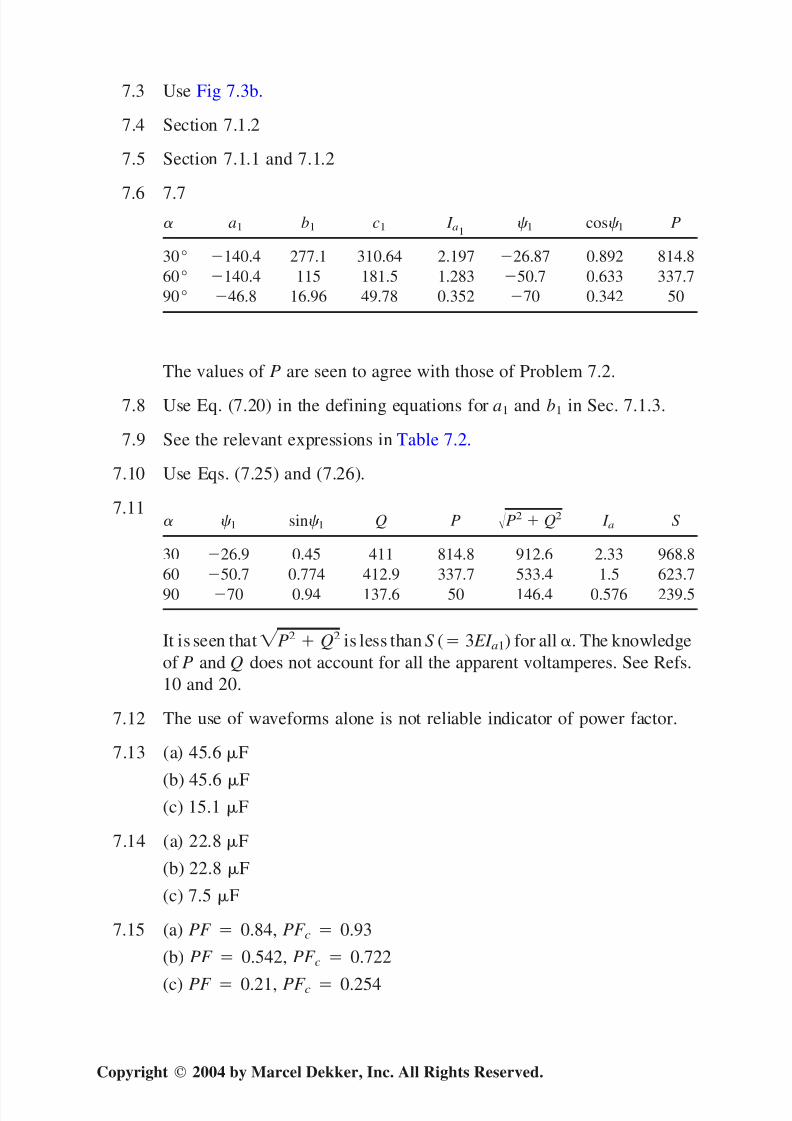
7.3 Use Fig 7.3b.
7.4 Section 7.1.2
7.5 Section 7.1.1 and 7.1.2
7.6 7.7 a1 b1 c1 I a1
1 cos 1 P
30° 140.4 277.1 310.64 2.197 26.87 0.892 814.8
60° 140.4 115 181.5 1.283 50.7 0.633 337.7
90° 46.8 16.96 49.78 0.352 70 0.342 50
The values of P are seen to agree with those of Problem 7.2.
7.8 Use Eq. (7.20) in the defining equations for a1 and b1 in Sec. 7.1.3.
7.9 See the relevant expressions in Table 7.2.
7.10 Use Eqs. (7.25) and (7.26).
7.11 1 sin 1 Q P P2
Q2 I a S
30 26.9 0.45 411 814.8 912.6 2.33 968.8
60 50.7 0.774 412.9 337.7 533.4 1.5 623.7
90 70 0.94 137.6 50 146.4 0.576 239.5
It is seen that P2Q2 is less than S ( 3 EI a1) for all . The knowledge
of P and Q does not account for all the apparent voltamperes. See Refs.
10 and 20.
7.12 The use of waveforms alone is not reliable indicator of power factor.
7.13 (a) 45.6 F
(b) 45.6 F(c) 15.1 F
7.14 (a) 22.8 F
(b) 22.8 F
(c) 7.5 F
7.15 (a) PF 0.84, PF c 0.93
(b) PF 0.542, PF c 0.722
(c) PF 0.21, PF c 0.254
Copyright 2004 by Marcel Dekker, Inc. All Rights Reserved.
8/13/2019 Dke090x Answers
http://slidepdf.com/reader/full/dke090x-answers 15/22
7.16 See Fig. 7.8.
7.17 See Eqs. (7.54)–(7.58)
7.18 (a) 235.8 W, 2436.5 W (b) 786 W, 1011 W
7.19 See Eq. (7.59).
7.20 QED question
7.21 See Eqs. (7.60) and (7.61).
7.22 Use Eq. (7.49), which has the value unity for 0.
7.23 (a) 3.96A at 30
(b) 2.29A at 60
7.24 587 V, 3.24 A
7.25 QED question
7.26 Use Eqs. (7.54) and (7.55).
7.27 Without compensation, PF 30 0.827, PF 60 0.477.
When X c R, PF 30 0.932, PF 60 0.792, 33.25.
7.28 See Eq. (7.68).
7.29 25.11 F PF 30 0.941 (0.827) PF 60 0.848 (0.477)
7.30 Waveforms questions-subjective
7.31Current distortion
factor = =( ) − ( )( ) + I
I
R X R X c1
2 218 2 18 / / / sin / π α π22
2
2
2 2 2 218 2 36
( )( ) − ( )( ) + ( )
cos
/ / / sin / cos
α
π α π α R X R X c
When the limiting condition of Eq. (7.66) is satisfied, then R / X c 18
sin2 / 2. This gives I 1 / I 3/ , which is the condition for resistive load.If R / X c 18sin2 / 2, then I 1 / I → 3/ .
7.32 Section 7.3.1
7.33 QED question
7.34 25.14 mH, 59.5
7.35 Eqs. (7.89)–(7.91)
7.36 3000 W, compared with 7358 W
Copyright 2004 by Marcel Dekker, Inc. All Rights Reserved.

8/13/2019 Dke090x Answers
http://slidepdf.com/reader/full/dke090x-answers 16/22
7.37 I m
I m
a
a
ο
ο
( )
( ).
=
==
15
00 975
7.38 (a) 0.927
(b) 0.802(c) 0.47
7.39 Section 7.3.1, Eq. (7.77)
7.40 Section 7.3.1, part (b), Eq. (7.97)
CHAPTER 8
8.1 Use the basic integral definition Eq. (2.7).8.2 (a) 1.03 V
(b) 0.9 V
8.3V
V
n
n n
V
n = − +
= ° =
41
6 3
120 0 811
ππ π
δ
cos cos
. V(cf. 1.1 V)
8.4 1 17.8 2 40
8.5 QED question
8.6 1 23.6 2 33.3
8.7 Graphical question
8.8 b1 0.99 V, b3 0.004 V, b5 0.001 V, b7 0.03 V, b9
0.21 V, b110.184 V, b13 0.11 V, b15 0.14 V, b170.02
V, b19 0.12 V, b21 0.01 V, brms 0.743 V.
CHAPTER 9
9.1 0, 12051 W, 11840 W, 10133 W
9.2 622 V, 37.24 A
9.3 154, P165 0, 52.6 kVA
9.4 933 V, 32.5 A
9.5 146.4
Copyright 2004 by Marcel Dekker, Inc. All Rights Reserved.

8/13/2019 Dke090x Answers
http://slidepdf.com/reader/full/dke090x-answers 17/22
9.6 0.675
9.7 I av 228 5A E av 218.81 kV
9.8 155
9.9 13.24
CHAPTER 10
10.1 See Figs. 10.3 and 10.4.
10.2 See Figs. 10.5 and 10.6.
V ab leads V an by 30
10.3 See Figs. 10.5–10.710.4 V V V V V NO dc AN dc BN = −( ) = −( )
π π
π0
2
(a) V NO is square wave V dc /3 with three times supply frequency.
(b) I NO is square wave V dc / R with three times supply frequency.
10.5 a b E
V E
V E
V E m m
avm
avm
1 1 1 20
3 3
2
2
3
6
1= = = = =
π π π
10.6 V t V t V t AB( ) . sin( ) sin( )ω ω π
ω = + ° = + °2 21 30 4 3 30
V t V
AB( )ω = =1
2
4
3 (wave average)
V t V
AB( ) .
.ω π
= = =1
2
2 210 703(wave average) V
Current wave form is shown in Fig. 10.7.
10.7 See Example 10.1
10.8a b
E c E E m
1 1 1 104
1
0 9
= = = = =
=π
ψ cos
.
rms
Distortion factor
10.9 ππ
ω ω π
π
3
60 732
6
3V t d t sin .
/
/
∫ =
10.10 V rms 0.732V b1 1.023 V
Distortion factor 0.99
Copyright 2004 by Marcel Dekker, Inc. All Rights Reserved.

8/13/2019 Dke090x Answers
http://slidepdf.com/reader/full/dke090x-answers 18/22
10.11 4.35 A, I dc 5.67 A, 1135 W
10.12 8.165 A, I dc 20 A ,400 W
10.13 8.723 A, 0.38 A
CHAPTER 11
11.1 b1 0.99 V, b3 0.004 V, b5 0.001 V, b7 0.03 V, b9
0.21 V, b110.184 V, b13 0.11 V, b15 0.14 V, b170.02V,
b19 0.12 V, b21 0.01 V, brms 0.743 V
11.2 I rms 5.013 A, CDF 0.999, VDF 0.942
11.3 628 W, 0.42
11.4 See Example 11.3 and Fig. 11.13.
11.5 I rms 32.72 A, I 1 32.65 A, I 11 1.72A, I 13 0.87 A, I 19 0.65
A
11.6 There are no triplen harmonic currents.
Pin 15421W, V rms 171 5V, I rms 32.72A, PF 0.915 lagging
11.7 (a) 89.6%(b) 81.1%
CHAPTER 12
12.1 (a) 114 V
(b) 103.2 V
(c) 81.5 V
(d) 51.02 V
(e) 19.9 V12.2 Lowest harmonic is the second-order harmonic.
12.3 (a) 109.8 V
(b) 95.1 V
(c) 54.9 V
(d) 0
12.4 E rms 302.3 V Pin 5.25 kW/phase
I out 70 A rms PF 0.43 lagging
Copyright 2004 by Marcel Dekker, Inc. All Rights Reserved.

8/13/2019 Dke090x Answers
http://slidepdf.com/reader/full/dke090x-answers 19/22
12.5 (a) 36
(b) I o 53.67 A (rms)
(c) P1 2880 W
(d) I in 31 A(rms)
(e) Irh 21.92 A (rms)
(f) PF 0.244 lagging
12.6 See section 12.3.1
12.7 3 f in 2 f o 193.33 166.67 Hz
3 f in 4 f o 206.66 153.34 Hz
3 f in 6 f o 220 140 Hz
3 f in 8 f o 233.33 126.67 Hz
12.8 6 f in f o 380 340 Hz
6 f in 3 f o 420 300 Hz
6 f in 5 f o 460 260 Hz
12.9 P1 Pin 151.4 kW
E o 420 V
cosin 0.77 lagging
I o 120 A
CHAPTER 13
13.1 M 1, 4, 7, 10, 13
13.2 The criteria are satisfied in all cases.
13.3 The combination M 11, M c 5, M s 3 does not satisfy Eq. (13.17)
and is not viable.
13.4 The combination M 8, M c 2, M s 3 satisfies both Eqs. (13.17)
and (13.19) and is an acceptable waveform.
13.5 M 1 2 3 4 5 6 7 8 9 10
o (Hz) 50 30 21.4 16.67 13.6 11.54 10 8.82 7.9 7.14
13.6 M c 3, M s 2, M 7
v w 120
Copyright 2004 by Marcel Dekker, Inc. All Rights Reserved.
8/13/2019 Dke090x Answers
http://slidepdf.com/reader/full/dke090x-answers 20/22
13.7 M c 3, M s 4, M 11
v w 109.6
13.8 (a) 12 Hz
(b) 7.83 Hz
(c) 6.67 Hz
13.9 M 6, M c 2, M s 2
v w 110.8
p =13
3
CHAPTER 14
There are no end-of-chapter problems for this section.
CHAPTER 15
15.1 V av kV s V rms kV s
15.2 P kV R
V
R
V
R
s
s
s
= 2
2
2
4
3
4
/
( )
( )
a
b
15.3 V switch (1 k )V s V diode kV s
15.4 T p 500 s f 2000 Hz
15.5 22.5 V
15.6 k 0.893 V o 1072 V
15.7 I 7 A
15.8 (a) 4486 Hz
(b) 169.42 s
(c) 26.18 A
15.9 (a) 135.85 A, 82.35 A
(b) I o 110.2 A, I sw 53.98 A, I d 96.1 A
Copyright 2004 by Marcel Dekker, Inc. All Rights Reserved.
8/13/2019 Dke090x Answers
http://slidepdf.com/reader/full/dke090x-answers 21/22
15.10 0.667–0.333
15.11 (a) 185 s
(b) 142.15 s
(c) 52 A
15.12 I in(max) 77.32 A, I in(min) 57.92 A, I in(av) 67.62 A
15.13 171 s
15.14 (a) 0.337 A, 58.67 V
(b) 3.034 A, 176 V
(c) 27.31 A, 528 V
15.15 (a) 16.67 V, 9 A
(b) 150 V, 81.1 A
15.16 (a) 2.79 A, 0.335 V at k 0.25
(b) 8.37 A, 9.05 V at k 0.75
CHAPTER 16
16.1 (a) 0.9 A
(b) 4.49 A
(c) 8.08 A
16.2 18 V
16.3 4.04 A
16.4 I 2 40 A, I 1 4.8 A
t 50 s, V L 13.46 V
16.5 15.6 H
16.6 1/2
16.7 48 V
16.8 1 /2 1 s
16.9 dim 105 mA
16.10 (a) 25 V
(b) 75 V
(c) 225 V
Copyright 2004 by Marcel Dekker, Inc. All Rights Reserved.
8/13/2019 Dke090x Answers
http://slidepdf.com/reader/full/dke090x-answers 22/22
16.11 k 1/2
16.12 V L 128.6 V, k 0.682
16.13 k 0.549, 1 15.71 s
16.14 (a) 8.89 s(b) 0.125 A
(c) 3.16 mJ
16.15 14 s, 9.04 s, 0.8 s
16.16 1 11.905 s, 0.5 s, 11.9 s, 0 s