dl305 analog i/o modules - automationdirect · pdf filege fanuc automation north america, inc...
TRANSCRIPT

DL305
Analog I/O Modules
Manual Number D3--ANLG-M

WARNING
Thank you for purchasing automation equipment from Automationdirect.com. We want your new DirectLOGICautomation equipment to operate safely. Anyone who installs or uses this equipment should read this publication (andany other relevant publications) before installing or operating the equipment.
To minimize the risk of potential safety problems, you should follow all applicable local and national codes that regulatethe installation and operation of your equipment. These codes vary from area to area and usually change with time. It isyour responsibility to determine which codes should be followed, and to verify that the equipment, installation, andoperation is in compliance with the latest revision of these codes.
At a minimum, you should follow all applicable sections of the National Fire Code, National Electrical Code, and thecodes of the National Electrical Manufacturer’s Association (NEMA). There may be local regulatory or governmentoffices that can also help determine which codes and standards are necessary for safe installation and operation.
Equipment damage or serious injury to personnel can result from the failure to follow all applicable codes andstandards. We do not guarantee the products described in this publication are suitable for your particular application,nor do we assume any responsibility for your product design, installation, or operation.
If you have any questions concerning the installation or operation of this equipment, or if you need additionalinformation, please call us at 1--770--844--4200 or FAX 1--770--886--3199.
This publication is based on information that was available at the time it was printed. At Automationdirect.com weconstantly strive to improve our products and services, so we reserve the right to make changes to the products and/orpublications at any time without notice and without any obligation. This publication may also discuss features that maynot be available in certain revisions of the product.
TrademarksThis publication may contain references to products produced and/or offered by other companies. The product andcompany names may be trademarked and are the sole property of their respective owners. Automationdirect.comdisclaims any proprietary interest in the marks and names of others.
Stage is a trademark of Koyo Electronics Industries Co., LTD. Think & Do Software is a trademark of Think & DoSoftware, Inc. Texas Instruments is a registered trademark of Texas Instruments, Inc. TI, TIWAY, Series 305, Series405, TI305, and TI405 are trademarks of Texas Instruments, Inc. Siemens and SIMATIC are registered trademarks ofSiemens, AG. GE is a registered trademark of General Electric Corporation. Series One is a registered trademark ofGE Fanuc Automation North America, Inc. MODBUS is a registered trademark of Gould, Inc. IBM is a registeredtrademark of International Business Machines. MS-DOS and Microsoft are registered trademarks of MicrosoftCorporation. Windows and Windows NT are trademarks of Microsoft Corporation. OPTOMUX and PAMUX aretrademarks of OPTO 22.
Copyright 1999, Automationdirect.com IncorporatedAll Rights Reserved
No part of this manual shall be copied, reproduced, or transmitted in any way without the prior, written consent ofAutomationdirect.com Incorporated. Automationdirect.com retains the exclusive rights to all informationincluded in this document.

1Manual RevisionsIf you contact us in reference to this manual, be sure to include the revision number.
Title: DL305 Analog I/O Modules, 2nd Edition, Rev. C
Manual Number: D3--ANLG--M
Issue Date Effective Pages Description of Changes
Original 1/94 Cover/CopyrightContentsManual Revisions1-1 -- 1-92-1 -- 2-183-1 -- 3-204-1 -- 4-155-1 -- 5-216-1 -- 6-127-1 -- 7-148-1 -- 8-179-1 -- 9-16
10-1 -- 10-14A-1 -- A-10
Original Issue
2nd Edition 3/96 Cover/CopyrightContentsManual Revisions1-1 -- 1-92-1 -- 2-183-1 -- 3-204-1 -- 4-155-1 -- 5-216-1 -- 6-137-1 -- 7-148-1 -- 8-189-1 -- 9-16
10-1 -- 10-14A-1 -- A-10
2nd Edition
Rev. A 4/96 Manual Revisions7--138--17
Rev. AChanged last instruction to DOUT3Changed last instruction to DOUT3
Rev. B 6/98 Entire ManualManual Revisions7--10, 7--11, 7--13 and 8--17
Downsized to spiralRev. BCorrected sequencing examples
Rev. C 11/99 3--13,18; 4--11,12,17;5-16to19,24; 9-12,13;10--14to16; Appx. A--11to19
Added example programs for the D3--350CPU.

1Table of ContentsChapter 1: Getting StartedIntroduction 1--2. . . . . . . . . . . . . . . . . . . . . . . . . . . . . . . . . . . . . . . . . . . . . . . . . . . . . . . . . . . . . . . . . . . . . . . . .
Purpose of this manual 1--3. . . . . . . . . . . . . . . . . . . . . . . . . . . . . . . . . . . . . . . . . . . . . . . . . . . . . . . . . . . . .Who should read this manual 1--3. . . . . . . . . . . . . . . . . . . . . . . . . . . . . . . . . . . . . . . . . . . . . . . . . . . . . . .How this manual is organized 1--3. . . . . . . . . . . . . . . . . . . . . . . . . . . . . . . . . . . . . . . . . . . . . . . . . . . . . . .Supplemental Manuals 1--3. . . . . . . . . . . . . . . . . . . . . . . . . . . . . . . . . . . . . . . . . . . . . . . . . . . . . . . . . . . . .
DL305 Analog Components 1--4. . . . . . . . . . . . . . . . . . . . . . . . . . . . . . . . . . . . . . . . . . . . . . . . . . . . . . . . . .DL305 Analog I/O 1--4. . . . . . . . . . . . . . . . . . . . . . . . . . . . . . . . . . . . . . . . . . . . . . . . . . . . . . . . . . . . . . . . .Thermocouple Input 1--4. . . . . . . . . . . . . . . . . . . . . . . . . . . . . . . . . . . . . . . . . . . . . . . . . . . . . . . . . . . . . . .Temperature Input 1--4. . . . . . . . . . . . . . . . . . . . . . . . . . . . . . . . . . . . . . . . . . . . . . . . . . . . . . . . . . . . . . . . .
Physical Characteristics 1--5. . . . . . . . . . . . . . . . . . . . . . . . . . . . . . . . . . . . . . . . . . . . . . . . . . . . . . . . . . . . .Selecting the Appropriate Module 1--6. . . . . . . . . . . . . . . . . . . . . . . . . . . . . . . . . . . . . . . . . . . . . . . . . . . .
Analog Input 1--6. . . . . . . . . . . . . . . . . . . . . . . . . . . . . . . . . . . . . . . . . . . . . . . . . . . . . . . . . . . . . . . . . . . . . .Analog Output 1--7. . . . . . . . . . . . . . . . . . . . . . . . . . . . . . . . . . . . . . . . . . . . . . . . . . . . . . . . . . . . . . . . . . . .Special Input 1--7. . . . . . . . . . . . . . . . . . . . . . . . . . . . . . . . . . . . . . . . . . . . . . . . . . . . . . . . . . . . . . . . . . . . .
Analog Made Easy -- Four Simple Steps 1--8. . . . . . . . . . . . . . . . . . . . . . . . . . . . . . . . . . . . . . . . . . . . . . .Analog Input Terminology 1--9. . . . . . . . . . . . . . . . . . . . . . . . . . . . . . . . . . . . . . . . . . . . . . . . . . . . . . . . . . . .
Channels per Module 1--9. . . . . . . . . . . . . . . . . . . . . . . . . . . . . . . . . . . . . . . . . . . . . . . . . . . . . . . . . . . . . .Input Ranges 1--9. . . . . . . . . . . . . . . . . . . . . . . . . . . . . . . . . . . . . . . . . . . . . . . . . . . . . . . . . . . . . . . . . . . . .Resolution 1--9. . . . . . . . . . . . . . . . . . . . . . . . . . . . . . . . . . . . . . . . . . . . . . . . . . . . . . . . . . . . . . . . . . . . . . . .Input Type 1--9. . . . . . . . . . . . . . . . . . . . . . . . . . . . . . . . . . . . . . . . . . . . . . . . . . . . . . . . . . . . . . . . . . . . . . . .Input Impedance 1--9. . . . . . . . . . . . . . . . . . . . . . . . . . . . . . . . . . . . . . . . . . . . . . . . . . . . . . . . . . . . . . . . . .Conversion Method 1--9. . . . . . . . . . . . . . . . . . . . . . . . . . . . . . . . . . . . . . . . . . . . . . . . . . . . . . . . . . . . . . . .Conversion Time 1--9. . . . . . . . . . . . . . . . . . . . . . . . . . . . . . . . . . . . . . . . . . . . . . . . . . . . . . . . . . . . . . . . . .Linearity Error and Total Tolerance (Relative Accuracy) 1--9. . . . . . . . . . . . . . . . . . . . . . . . . . . . . . . . .Accuracy vs. Temperature 1--9. . . . . . . . . . . . . . . . . . . . . . . . . . . . . . . . . . . . . . . . . . . . . . . . . . . . . . . . . .LED Display 1--9. . . . . . . . . . . . . . . . . . . . . . . . . . . . . . . . . . . . . . . . . . . . . . . . . . . . . . . . . . . . . . . . . . . . . .I/O Points Required 1--9. . . . . . . . . . . . . . . . . . . . . . . . . . . . . . . . . . . . . . . . . . . . . . . . . . . . . . . . . . . . . . . .External Power Source 1--9. . . . . . . . . . . . . . . . . . . . . . . . . . . . . . . . . . . . . . . . . . . . . . . . . . . . . . . . . . . . .Base Power Required 1--9. . . . . . . . . . . . . . . . . . . . . . . . . . . . . . . . . . . . . . . . . . . . . . . . . . . . . . . . . . . . . .Operating Temperature 1--9. . . . . . . . . . . . . . . . . . . . . . . . . . . . . . . . . . . . . . . . . . . . . . . . . . . . . . . . . . . .Relative Humidity 1--9. . . . . . . . . . . . . . . . . . . . . . . . . . . . . . . . . . . . . . . . . . . . . . . . . . . . . . . . . . . . . . . . .Terminal Type 1--9. . . . . . . . . . . . . . . . . . . . . . . . . . . . . . . . . . . . . . . . . . . . . . . . . . . . . . . . . . . . . . . . . . . . .Weight 1--9. . . . . . . . . . . . . . . . . . . . . . . . . . . . . . . . . . . . . . . . . . . . . . . . . . . . . . . . . . . . . . . . . . . . . . . . . . .
Analog Output Module Terminology 1--10. . . . . . . . . . . . . . . . . . . . . . . . . . . . . . . . . . . . . . . . . . . . . . . . . .Channels per Module 1--10. . . . . . . . . . . . . . . . . . . . . . . . . . . . . . . . . . . . . . . . . . . . . . . . . . . . . . . . . . . . . .Output Ranges 1--10. . . . . . . . . . . . . . . . . . . . . . . . . . . . . . . . . . . . . . . . . . . . . . . . . . . . . . . . . . . . . . . . . . . .Resolution 1--10. . . . . . . . . . . . . . . . . . . . . . . . . . . . . . . . . . . . . . . . . . . . . . . . . . . . . . . . . . . . . . . . . . . . . . . .Output Current 1--10. . . . . . . . . . . . . . . . . . . . . . . . . . . . . . . . . . . . . . . . . . . . . . . . . . . . . . . . . . . . . . . . . . . .Output Impedance 1--10. . . . . . . . . . . . . . . . . . . . . . . . . . . . . . . . . . . . . . . . . . . . . . . . . . . . . . . . . . . . . . . .Load Impedance 1--10. . . . . . . . . . . . . . . . . . . . . . . . . . . . . . . . . . . . . . . . . . . . . . . . . . . . . . . . . . . . . . . . . .Conversion Time 1--10. . . . . . . . . . . . . . . . . . . . . . . . . . . . . . . . . . . . . . . . . . . . . . . . . . . . . . . . . . . . . . . . . .Accuracy 1--10. . . . . . . . . . . . . . . . . . . . . . . . . . . . . . . . . . . . . . . . . . . . . . . . . . . . . . . . . . . . . . . . . . . . . . . . .Accuracy vs. Temperature 1--10. . . . . . . . . . . . . . . . . . . . . . . . . . . . . . . . . . . . . . . . . . . . . . . . . . . . . . . . . .LED Display 1--10. . . . . . . . . . . . . . . . . . . . . . . . . . . . . . . . . . . . . . . . . . . . . . . . . . . . . . . . . . . . . . . . . . . . . .

iiTable of Contents
External Power Source 1--10. . . . . . . . . . . . . . . . . . . . . . . . . . . . . . . . . . . . . . . . . . . . . . . . . . . . . . . . . . . . .Base Power Required 1--10. . . . . . . . . . . . . . . . . . . . . . . . . . . . . . . . . . . . . . . . . . . . . . . . . . . . . . . . . . . . . .Operating Temperature 1--10. . . . . . . . . . . . . . . . . . . . . . . . . . . . . . . . . . . . . . . . . . . . . . . . . . . . . . . . . . . .Relative Humidity 1--10. . . . . . . . . . . . . . . . . . . . . . . . . . . . . . . . . . . . . . . . . . . . . . . . . . . . . . . . . . . . . . . . .Terminal Type 1--10. . . . . . . . . . . . . . . . . . . . . . . . . . . . . . . . . . . . . . . . . . . . . . . . . . . . . . . . . . . . . . . . . . . . .Weight 1--10. . . . . . . . . . . . . . . . . . . . . . . . . . . . . . . . . . . . . . . . . . . . . . . . . . . . . . . . . . . . . . . . . . . . . . . . . . .I/O Points Required 1--10. . . . . . . . . . . . . . . . . . . . . . . . . . . . . . . . . . . . . . . . . . . . . . . . . . . . . . . . . . . . . . . .
Chapter 2: D3--04AD 4-Channel Analog InputModule Specifications 2--2. . . . . . . . . . . . . . . . . . . . . . . . . . . . . . . . . . . . . . . . . . . . . . . . . . . . . . . . . . . . . . .
Analog Input Configuration Requirements 2--2. . . . . . . . . . . . . . . . . . . . . . . . . . . . . . . . . . . . . . . . . . . .Setting the Module Jumpers 2--3. . . . . . . . . . . . . . . . . . . . . . . . . . . . . . . . . . . . . . . . . . . . . . . . . . . . . . . . .
Connecting the Field Wiring 2--3. . . . . . . . . . . . . . . . . . . . . . . . . . . . . . . . . . . . . . . . . . . . . . . . . . . . . . . . . .Wiring Guidelines 2--3. . . . . . . . . . . . . . . . . . . . . . . . . . . . . . . . . . . . . . . . . . . . . . . . . . . . . . . . . . . . . . . . .User Power Supply Requirements 2--3. . . . . . . . . . . . . . . . . . . . . . . . . . . . . . . . . . . . . . . . . . . . . . . . . . .Custom Input Ranges 2--4. . . . . . . . . . . . . . . . . . . . . . . . . . . . . . . . . . . . . . . . . . . . . . . . . . . . . . . . . . . . . .Current Loop Transmitter Impedance 2--5. . . . . . . . . . . . . . . . . . . . . . . . . . . . . . . . . . . . . . . . . . . . . . . .Removable Connector 2--6. . . . . . . . . . . . . . . . . . . . . . . . . . . . . . . . . . . . . . . . . . . . . . . . . . . . . . . . . . . . .Wiring Diagram 2--6. . . . . . . . . . . . . . . . . . . . . . . . . . . . . . . . . . . . . . . . . . . . . . . . . . . . . . . . . . . . . . . . . . .
Module Operation 2--7. . . . . . . . . . . . . . . . . . . . . . . . . . . . . . . . . . . . . . . . . . . . . . . . . . . . . . . . . . . . . . . . . . .Channel Scanning Sequence 2--7. . . . . . . . . . . . . . . . . . . . . . . . . . . . . . . . . . . . . . . . . . . . . . . . . . . . . . .Understanding the I/O Assignments 2--8. . . . . . . . . . . . . . . . . . . . . . . . . . . . . . . . . . . . . . . . . . . . . . . . .All Channel Scan Output 2--8. . . . . . . . . . . . . . . . . . . . . . . . . . . . . . . . . . . . . . . . . . . . . . . . . . . . . . . . . . .Single Channel Scan Outputs 2--9. . . . . . . . . . . . . . . . . . . . . . . . . . . . . . . . . . . . . . . . . . . . . . . . . . . . . . .Active Channel Selection Inputs 2--9. . . . . . . . . . . . . . . . . . . . . . . . . . . . . . . . . . . . . . . . . . . . . . . . . . . . .Analog Data Bits 2--10. . . . . . . . . . . . . . . . . . . . . . . . . . . . . . . . . . . . . . . . . . . . . . . . . . . . . . . . . . . . . . . . . .
Writing the Control Program 2--11. . . . . . . . . . . . . . . . . . . . . . . . . . . . . . . . . . . . . . . . . . . . . . . . . . . . . . . . .Identifying the Data Locations 2--11. . . . . . . . . . . . . . . . . . . . . . . . . . . . . . . . . . . . . . . . . . . . . . . . . . . . . . .Single Channel on Every Scan 2--11. . . . . . . . . . . . . . . . . . . . . . . . . . . . . . . . . . . . . . . . . . . . . . . . . . . . . .Reading Multiple Channels over Alternating Scans 2--12. . . . . . . . . . . . . . . . . . . . . . . . . . . . . . . . . . . .Single or Multiple Channels 2--13. . . . . . . . . . . . . . . . . . . . . . . . . . . . . . . . . . . . . . . . . . . . . . . . . . . . . . . . .Scaling the Input Data 2--14. . . . . . . . . . . . . . . . . . . . . . . . . . . . . . . . . . . . . . . . . . . . . . . . . . . . . . . . . . . . .Analog and Digital Value Conversions 2--18. . . . . . . . . . . . . . . . . . . . . . . . . . . . . . . . . . . . . . . . . . . . . . . .
Chapter 3: F3--04ADS 4-Channel Isolated Analog InputModule Specifications 3--2. . . . . . . . . . . . . . . . . . . . . . . . . . . . . . . . . . . . . . . . . . . . . . . . . . . . . . . . . . . . . . .
Analog Input Configuration Requirements 3--2. . . . . . . . . . . . . . . . . . . . . . . . . . . . . . . . . . . . . . . . . . . .Setting the Module Jumpers 3--3. . . . . . . . . . . . . . . . . . . . . . . . . . . . . . . . . . . . . . . . . . . . . . . . . . . . . . . . .
Jumper Locations 3--3. . . . . . . . . . . . . . . . . . . . . . . . . . . . . . . . . . . . . . . . . . . . . . . . . . . . . . . . . . . . . . . . .Selecting the Number of Channels 3--4. . . . . . . . . . . . . . . . . . . . . . . . . . . . . . . . . . . . . . . . . . . . . . . . . . .Selecting Input Signal Ranges 3--4. . . . . . . . . . . . . . . . . . . . . . . . . . . . . . . . . . . . . . . . . . . . . . . . . . . . . .
Connecting the Field Wiring 3--5. . . . . . . . . . . . . . . . . . . . . . . . . . . . . . . . . . . . . . . . . . . . . . . . . . . . . . . . . .Wiring Guidelines 3--5. . . . . . . . . . . . . . . . . . . . . . . . . . . . . . . . . . . . . . . . . . . . . . . . . . . . . . . . . . . . . . . . .User Power Supply Requirements 3--5. . . . . . . . . . . . . . . . . . . . . . . . . . . . . . . . . . . . . . . . . . . . . . . . . . .Custom Input Ranges 3--5. . . . . . . . . . . . . . . . . . . . . . . . . . . . . . . . . . . . . . . . . . . . . . . . . . . . . . . . . . . . . .Current Loop Transmitter Impedance 3--6. . . . . . . . . . . . . . . . . . . . . . . . . . . . . . . . . . . . . . . . . . . . . . . .Removable Connector 3--7. . . . . . . . . . . . . . . . . . . . . . . . . . . . . . . . . . . . . . . . . . . . . . . . . . . . . . . . . . . . .Wiring Diagram 3--7. . . . . . . . . . . . . . . . . . . . . . . . . . . . . . . . . . . . . . . . . . . . . . . . . . . . . . . . . . . . . . . . . . .

iiiTable of Contents
Module Operation 3--8. . . . . . . . . . . . . . . . . . . . . . . . . . . . . . . . . . . . . . . . . . . . . . . . . . . . . . . . . . . . . . . . . . .Channel Scanning Sequence 3--8. . . . . . . . . . . . . . . . . . . . . . . . . . . . . . . . . . . . . . . . . . . . . . . . . . . . . . .Understanding the I/O Assignments 3--9. . . . . . . . . . . . . . . . . . . . . . . . . . . . . . . . . . . . . . . . . . . . . . . . .Active Channel Selection Inputs 3--9. . . . . . . . . . . . . . . . . . . . . . . . . . . . . . . . . . . . . . . . . . . . . . . . . . . . .Analog Data Bits 3--10. . . . . . . . . . . . . . . . . . . . . . . . . . . . . . . . . . . . . . . . . . . . . . . . . . . . . . . . . . . . . . . . . .
Writing the Control Program 3--11. . . . . . . . . . . . . . . . . . . . . . . . . . . . . . . . . . . . . . . . . . . . . . . . . . . . . . . . .Identifying the Data Locations 3--11. . . . . . . . . . . . . . . . . . . . . . . . . . . . . . . . . . . . . . . . . . . . . . . . . . . . . . .Single Channel on Every Scan 3--11. . . . . . . . . . . . . . . . . . . . . . . . . . . . . . . . . . . . . . . . . . . . . . . . . . . . . .Reading Multiple Channels over Alternating Scans 3--12. . . . . . . . . . . . . . . . . . . . . . . . . . . . . . . . . . . .Scaling the Input Data 3--13. . . . . . . . . . . . . . . . . . . . . . . . . . . . . . . . . . . . . . . . . . . . . . . . . . . . . . . . . . . . .Analog and Digital Value Conversions 3--1. . . . . . . . . . . . . . . . . . . . . . . . . . . . . . . . . . . . . . . . . . . . . . . .
Chapter 4: F3--08AD 8-Channel Analog InputModule Specifications 4--2. . . . . . . . . . . . . . . . . . . . . . . . . . . . . . . . . . . . . . . . . . . . . . . . . . . . . . . . . . . . . . .
Analog Input Configuration Requirements 4--2. . . . . . . . . . . . . . . . . . . . . . . . . . . . . . . . . . . . . . . . . . . .Setting the Module Jumpers 4--3. . . . . . . . . . . . . . . . . . . . . . . . . . . . . . . . . . . . . . . . . . . . . . . . . . . . . . . . .
Jumper Locations 4--3. . . . . . . . . . . . . . . . . . . . . . . . . . . . . . . . . . . . . . . . . . . . . . . . . . . . . . . . . . . . . . . . .Selecting the Number of Channels 4--3. . . . . . . . . . . . . . . . . . . . . . . . . . . . . . . . . . . . . . . . . . . . . . . . . . .
Connecting the Field Wiring 4--4. . . . . . . . . . . . . . . . . . . . . . . . . . . . . . . . . . . . . . . . . . . . . . . . . . . . . . . . . .Wiring Guidelines 4--4. . . . . . . . . . . . . . . . . . . . . . . . . . . . . . . . . . . . . . . . . . . . . . . . . . . . . . . . . . . . . . . . .User Power Supply Requirements 4--4. . . . . . . . . . . . . . . . . . . . . . . . . . . . . . . . . . . . . . . . . . . . . . . . . . .Current Loop Transmitter Impedance 4--4. . . . . . . . . . . . . . . . . . . . . . . . . . . . . . . . . . . . . . . . . . . . . . . .Removable Connector 4--5. . . . . . . . . . . . . . . . . . . . . . . . . . . . . . . . . . . . . . . . . . . . . . . . . . . . . . . . . . . . .Wiring Diagram 4--5. . . . . . . . . . . . . . . . . . . . . . . . . . . . . . . . . . . . . . . . . . . . . . . . . . . . . . . . . . . . . . . . . . .
Module Operation 4--6. . . . . . . . . . . . . . . . . . . . . . . . . . . . . . . . . . . . . . . . . . . . . . . . . . . . . . . . . . . . . . . . . . .Channel Scanning Sequence 4--6. . . . . . . . . . . . . . . . . . . . . . . . . . . . . . . . . . . . . . . . . . . . . . . . . . . . . . .Understanding the I/O Assignments 4--7. . . . . . . . . . . . . . . . . . . . . . . . . . . . . . . . . . . . . . . . . . . . . . . . .Active Channel Indication Inputs 4--7. . . . . . . . . . . . . . . . . . . . . . . . . . . . . . . . . . . . . . . . . . . . . . . . . . . .Analog Data Bits 4--8. . . . . . . . . . . . . . . . . . . . . . . . . . . . . . . . . . . . . . . . . . . . . . . . . . . . . . . . . . . . . . . . . .
Writing the Control Program 4--9. . . . . . . . . . . . . . . . . . . . . . . . . . . . . . . . . . . . . . . . . . . . . . . . . . . . . . . . .Identifying the Data Locations 4--9. . . . . . . . . . . . . . . . . . . . . . . . . . . . . . . . . . . . . . . . . . . . . . . . . . . . . . .Single Channel on Every Scan 4--9. . . . . . . . . . . . . . . . . . . . . . . . . . . . . . . . . . . . . . . . . . . . . . . . . . . . . .Reading Multiple Channels over Alternating Scans 4--10. . . . . . . . . . . . . . . . . . . . . . . . . . . . . . . . . . . .Reading Multiple Channels over Alternating Scans on a DL350 4--11. . . . . . . . . . . . . . . . . . . . . . . . . .Scaling the Input Data 4--13. . . . . . . . . . . . . . . . . . . . . . . . . . . . . . . . . . . . . . . . . . . . . . . . . . . . . . . . . . . . .Scaling the Input Data on a DL350 4--17. . . . . . . . . . . . . . . . . . . . . . . . . . . . . . . . . . . . . . . . . . . . . . . . . .Analog and Digital Value Conversions 4--18. . . . . . . . . . . . . . . . . . . . . . . . . . . . . . . . . . . . . . . . . . . . . . . .
Chapter 5: F3--16AD 16-Channel Analog InputModule Specifications 5--2. . . . . . . . . . . . . . . . . . . . . . . . . . . . . . . . . . . . . . . . . . . . . . . . . . . . . . . . . . . . . . .
Analog Input Configuration Requirements 5--2. . . . . . . . . . . . . . . . . . . . . . . . . . . . . . . . . . . . . . . . . . . .Setting the Module Jumpers 5--3. . . . . . . . . . . . . . . . . . . . . . . . . . . . . . . . . . . . . . . . . . . . . . . . . . . . . . . . .
Jumper Locations 5--3. . . . . . . . . . . . . . . . . . . . . . . . . . . . . . . . . . . . . . . . . . . . . . . . . . . . . . . . . . . . . . . . .Selecting the Number of Channels 5--3. . . . . . . . . . . . . . . . . . . . . . . . . . . . . . . . . . . . . . . . . . . . . . . . . . .Selecting Input Signal Ranges 5--4. . . . . . . . . . . . . . . . . . . . . . . . . . . . . . . . . . . . . . . . . . . . . . . . . . . . . .Gain Jumpers 5--5. . . . . . . . . . . . . . . . . . . . . . . . . . . . . . . . . . . . . . . . . . . . . . . . . . . . . . . . . . . . . . . . . . . . .Variable Gain Adjustment 5--5. . . . . . . . . . . . . . . . . . . . . . . . . . . . . . . . . . . . . . . . . . . . . . . . . . . . . . . . . .

ivTable of Contents
Connecting the Field Wiring 5--6. . . . . . . . . . . . . . . . . . . . . . . . . . . . . . . . . . . . . . . . . . . . . . . . . . . . . . . . . .Wiring Guidelines 5--6. . . . . . . . . . . . . . . . . . . . . . . . . . . . . . . . . . . . . . . . . . . . . . . . . . . . . . . . . . . . . . . . .User Power Supply Requirements 5--6. . . . . . . . . . . . . . . . . . . . . . . . . . . . . . . . . . . . . . . . . . . . . . . . . . .Custom Input Ranges 5--7. . . . . . . . . . . . . . . . . . . . . . . . . . . . . . . . . . . . . . . . . . . . . . . . . . . . . . . . . . . . . .Current Loop Transmitter Impedance 5--8. . . . . . . . . . . . . . . . . . . . . . . . . . . . . . . . . . . . . . . . . . . . . . . .Removable Connector 5--9. . . . . . . . . . . . . . . . . . . . . . . . . . . . . . . . . . . . . . . . . . . . . . . . . . . . . . . . . . . . .Wiring Diagram 5--9. . . . . . . . . . . . . . . . . . . . . . . . . . . . . . . . . . . . . . . . . . . . . . . . . . . . . . . . . . . . . . . . . . .
Module Operation 5--10. . . . . . . . . . . . . . . . . . . . . . . . . . . . . . . . . . . . . . . . . . . . . . . . . . . . . . . . . . . . . . . . . . .Channel Scanning Sequence 5--10. . . . . . . . . . . . . . . . . . . . . . . . . . . . . . . . . . . . . . . . . . . . . . . . . . . . . . .Understanding the I/O Assignments 5--11. . . . . . . . . . . . . . . . . . . . . . . . . . . . . . . . . . . . . . . . . . . . . . . . .Active Channel Indicator Inputs 5--12. . . . . . . . . . . . . . . . . . . . . . . . . . . . . . . . . . . . . . . . . . . . . . . . . . . . .Analog Data Bits 5--13. . . . . . . . . . . . . . . . . . . . . . . . . . . . . . . . . . . . . . . . . . . . . . . . . . . . . . . . . . . . . . . . . .
Writing the Control Program 5--14. . . . . . . . . . . . . . . . . . . . . . . . . . . . . . . . . . . . . . . . . . . . . . . . . . . . . . . . .Identifying the Data Locations 5--14. . . . . . . . . . . . . . . . . . . . . . . . . . . . . . . . . . . . . . . . . . . . . . . . . . . . . . .Example Program 5--15. . . . . . . . . . . . . . . . . . . . . . . . . . . . . . . . . . . . . . . . . . . . . . . . . . . . . . . . . . . . . . . . .Example Program for a DL350 with a Conventional Base 5--16. . . . . . . . . . . . . . . . . . . . . . . . . . . . . . .Example Program for a DL350 with a D3--XX--1 Base 5--17. . . . . . . . . . . . . . . . . . . . . . . . . . . . . . . . . .Scaling the Input Data 5--20. . . . . . . . . . . . . . . . . . . . . . . . . . . . . . . . . . . . . . . . . . . . . . . . . . . . . . . . . . . . .Scaling the Input Data on a DL350 with a Conventional Base 5--24. . . . . . . . . . . . . . . . . . . . . . . . . . .Broken Transmitter Detection 5--25. . . . . . . . . . . . . . . . . . . . . . . . . . . . . . . . . . . . . . . . . . . . . . . . . . . . . . .Analog and Digital Value Conversions 5--26. . . . . . . . . . . . . . . . . . . . . . . . . . . . . . . . . . . . . . . . . . . . . . . .
Chapter 6: D3--02DA 2--Channel Analog OutputModule Specifications 6--2. . . . . . . . . . . . . . . . . . . . . . . . . . . . . . . . . . . . . . . . . . . . . . . . . . . . . . . . . . . . . . .
Analog Output Configuration Requirements 6--2. . . . . . . . . . . . . . . . . . . . . . . . . . . . . . . . . . . . . . . . . . .Connecting the Field Wiring 6--3. . . . . . . . . . . . . . . . . . . . . . . . . . . . . . . . . . . . . . . . . . . . . . . . . . . . . . . . . .
Wiring Guidelines 6--3. . . . . . . . . . . . . . . . . . . . . . . . . . . . . . . . . . . . . . . . . . . . . . . . . . . . . . . . . . . . . . . . .User Power Supply Requirements 6--3. . . . . . . . . . . . . . . . . . . . . . . . . . . . . . . . . . . . . . . . . . . . . . . . . . .Load Requirements 6--3. . . . . . . . . . . . . . . . . . . . . . . . . . . . . . . . . . . . . . . . . . . . . . . . . . . . . . . . . . . . . . . .Removable Connector 6--4. . . . . . . . . . . . . . . . . . . . . . . . . . . . . . . . . . . . . . . . . . . . . . . . . . . . . . . . . . . . .Wiring Diagram 6--4. . . . . . . . . . . . . . . . . . . . . . . . . . . . . . . . . . . . . . . . . . . . . . . . . . . . . . . . . . . . . . . . . . .
Module Operation 6--5. . . . . . . . . . . . . . . . . . . . . . . . . . . . . . . . . . . . . . . . . . . . . . . . . . . . . . . . . . . . . . . . . . .Channel Scanning Sequence 6--5. . . . . . . . . . . . . . . . . . . . . . . . . . . . . . . . . . . . . . . . . . . . . . . . . . . . . . .Understanding the I/O Assignments 6--6. . . . . . . . . . . . . . . . . . . . . . . . . . . . . . . . . . . . . . . . . . . . . . . . .Analog Data Bits 6--7. . . . . . . . . . . . . . . . . . . . . . . . . . . . . . . . . . . . . . . . . . . . . . . . . . . . . . . . . . . . . . . . . .
Writing the Control Program 6--8. . . . . . . . . . . . . . . . . . . . . . . . . . . . . . . . . . . . . . . . . . . . . . . . . . . . . . . . .Identifying the Data Locations 6--8. . . . . . . . . . . . . . . . . . . . . . . . . . . . . . . . . . . . . . . . . . . . . . . . . . . . . . .Calculating the Digital Value 6--8. . . . . . . . . . . . . . . . . . . . . . . . . . . . . . . . . . . . . . . . . . . . . . . . . . . . . . . .Sending the Same Data to Both Channels 6--11. . . . . . . . . . . . . . . . . . . . . . . . . . . . . . . . . . . . . . . . . . . .Sending Specific Data to Each Channel 6--12. . . . . . . . . . . . . . . . . . . . . . . . . . . . . . . . . . . . . . . . . . . . . .Analog and Digital Value Conversions 6--13. . . . . . . . . . . . . . . . . . . . . . . . . . . . . . . . . . . . . . . . . . . . . . . .
Chapter 7: F3--04DA--1 4-Channel Analog OutputModule Specifications 7--2. . . . . . . . . . . . . . . . . . . . . . . . . . . . . . . . . . . . . . . . . . . . . . . . . . . . . . . . . . . . . . .
Analog Output Configuration Requirements 7--2. . . . . . . . . . . . . . . . . . . . . . . . . . . . . . . . . . . . . . . . . . .Setting the Module Jumpers 7--3. . . . . . . . . . . . . . . . . . . . . . . . . . . . . . . . . . . . . . . . . . . . . . . . . . . . . . . . .
Jumper Locations 7--3. . . . . . . . . . . . . . . . . . . . . . . . . . . . . . . . . . . . . . . . . . . . . . . . . . . . . . . . . . . . . . . . .

vTable of Contents
Selecting Output Signal Ranges 7--3. . . . . . . . . . . . . . . . . . . . . . . . . . . . . . . . . . . . . . . . . . . . . . . . . . . . .Connecting the Field Wiring 7--4. . . . . . . . . . . . . . . . . . . . . . . . . . . . . . . . . . . . . . . . . . . . . . . . . . . . . . . . . .
Wiring Guidelines 7--4. . . . . . . . . . . . . . . . . . . . . . . . . . . . . . . . . . . . . . . . . . . . . . . . . . . . . . . . . . . . . . . . .User Power Supply Requirements 7--4. . . . . . . . . . . . . . . . . . . . . . . . . . . . . . . . . . . . . . . . . . . . . . . . . . .Load Requirements 7--4. . . . . . . . . . . . . . . . . . . . . . . . . . . . . . . . . . . . . . . . . . . . . . . . . . . . . . . . . . . . . . . .Removable Connector 7--5. . . . . . . . . . . . . . . . . . . . . . . . . . . . . . . . . . . . . . . . . . . . . . . . . . . . . . . . . . . . .Wiring Diagram 7--5. . . . . . . . . . . . . . . . . . . . . . . . . . . . . . . . . . . . . . . . . . . . . . . . . . . . . . . . . . . . . . . . . . .
Module Operation 7--6. . . . . . . . . . . . . . . . . . . . . . . . . . . . . . . . . . . . . . . . . . . . . . . . . . . . . . . . . . . . . . . . . . .Channel Scanning Sequence 7--6. . . . . . . . . . . . . . . . . . . . . . . . . . . . . . . . . . . . . . . . . . . . . . . . . . . . . . .Understanding the I/O Assignments 7--7. . . . . . . . . . . . . . . . . . . . . . . . . . . . . . . . . . . . . . . . . . . . . . . . .Channel Selection Inputs 7--7. . . . . . . . . . . . . . . . . . . . . . . . . . . . . . . . . . . . . . . . . . . . . . . . . . . . . . . . . . .Analog Data Bits 7--8. . . . . . . . . . . . . . . . . . . . . . . . . . . . . . . . . . . . . . . . . . . . . . . . . . . . . . . . . . . . . . . . . .
Writing the Control Program 7--9. . . . . . . . . . . . . . . . . . . . . . . . . . . . . . . . . . . . . . . . . . . . . . . . . . . . . . . . .Identifying the Data Locations 7--9. . . . . . . . . . . . . . . . . . . . . . . . . . . . . . . . . . . . . . . . . . . . . . . . . . . . . . .Calculating the Digital Value 7--9. . . . . . . . . . . . . . . . . . . . . . . . . . . . . . . . . . . . . . . . . . . . . . . . . . . . . . . .Sending Data to a Single Channel 7--12. . . . . . . . . . . . . . . . . . . . . . . . . . . . . . . . . . . . . . . . . . . . . . . . . . .Sequencing the Channel Updates 7--13. . . . . . . . . . . . . . . . . . . . . . . . . . . . . . . . . . . . . . . . . . . . . . . . . . .Sequencing Example 7--13. . . . . . . . . . . . . . . . . . . . . . . . . . . . . . . . . . . . . . . . . . . . . . . . . . . . . . . . . . . . . .Analog and Digital Value Conversions 7--14. . . . . . . . . . . . . . . . . . . . . . . . . . . . . . . . . . . . . . . . . . . . . . . .
Chapter 8: F3--04DAS 4-Channel Isolated Analog OutputModule Specifications 8--2. . . . . . . . . . . . . . . . . . . . . . . . . . . . . . . . . . . . . . . . . . . . . . . . . . . . . . . . . . . . . . .
Analog Output Configuration Requirements 8--3. . . . . . . . . . . . . . . . . . . . . . . . . . . . . . . . . . . . . . . . . . .Setting the Module Jumpers 8--4. . . . . . . . . . . . . . . . . . . . . . . . . . . . . . . . . . . . . . . . . . . . . . . . . . . . . . . . .
Jumper Locations 8--4. . . . . . . . . . . . . . . . . . . . . . . . . . . . . . . . . . . . . . . . . . . . . . . . . . . . . . . . . . . . . . . . .Selecting Input Signal Ranges 8--5. . . . . . . . . . . . . . . . . . . . . . . . . . . . . . . . . . . . . . . . . . . . . . . . . . . . . .Special Output Signal Ranges 8--6. . . . . . . . . . . . . . . . . . . . . . . . . . . . . . . . . . . . . . . . . . . . . . . . . . . . . .
Connecting the Field Wiring 8--7. . . . . . . . . . . . . . . . . . . . . . . . . . . . . . . . . . . . . . . . . . . . . . . . . . . . . . . . . .Wiring Guidelines 8--7. . . . . . . . . . . . . . . . . . . . . . . . . . . . . . . . . . . . . . . . . . . . . . . . . . . . . . . . . . . . . . . . .User Power Supply Requirements 8--7. . . . . . . . . . . . . . . . . . . . . . . . . . . . . . . . . . . . . . . . . . . . . . . . . . .Load Requirements 8--7. . . . . . . . . . . . . . . . . . . . . . . . . . . . . . . . . . . . . . . . . . . . . . . . . . . . . . . . . . . . . . . .Removable Connector 8--8. . . . . . . . . . . . . . . . . . . . . . . . . . . . . . . . . . . . . . . . . . . . . . . . . . . . . . . . . . . . .Wiring Diagram 8--8. . . . . . . . . . . . . . . . . . . . . . . . . . . . . . . . . . . . . . . . . . . . . . . . . . . . . . . . . . . . . . . . . . .Combining Voltage Outputs 8--8. . . . . . . . . . . . . . . . . . . . . . . . . . . . . . . . . . . . . . . . . . . . . . . . . . . . . . . . .Combining Current Outputs 8--9. . . . . . . . . . . . . . . . . . . . . . . . . . . . . . . . . . . . . . . . . . . . . . . . . . . . . . . . .
Module Operation 8--10. . . . . . . . . . . . . . . . . . . . . . . . . . . . . . . . . . . . . . . . . . . . . . . . . . . . . . . . . . . . . . . . . . .Channel Scanning Sequence 8--10. . . . . . . . . . . . . . . . . . . . . . . . . . . . . . . . . . . . . . . . . . . . . . . . . . . . . . .Understanding the I/O Assignments 8--11. . . . . . . . . . . . . . . . . . . . . . . . . . . . . . . . . . . . . . . . . . . . . . . . .Channel Selection Inputs 8--11. . . . . . . . . . . . . . . . . . . . . . . . . . . . . . . . . . . . . . . . . . . . . . . . . . . . . . . . . . .Analog Data Bits 8--12. . . . . . . . . . . . . . . . . . . . . . . . . . . . . . . . . . . . . . . . . . . . . . . . . . . . . . . . . . . . . . . . . .
Writing the Control Program 8--13. . . . . . . . . . . . . . . . . . . . . . . . . . . . . . . . . . . . . . . . . . . . . . . . . . . . . . . . .Identifying the Data Locations 8--13. . . . . . . . . . . . . . . . . . . . . . . . . . . . . . . . . . . . . . . . . . . . . . . . . . . . . . .Calculating the Digital Value 8--13. . . . . . . . . . . . . . . . . . . . . . . . . . . . . . . . . . . . . . . . . . . . . . . . . . . . . . . .Sending Data to a Single Channel 8--16. . . . . . . . . . . . . . . . . . . . . . . . . . . . . . . . . . . . . . . . . . . . . . . . . . .Sequencing the Channel Updates 8--17. . . . . . . . . . . . . . . . . . . . . . . . . . . . . . . . . . . . . . . . . . . . . . . . . . .Analog and Digital Value Conversions 8--18. . . . . . . . . . . . . . . . . . . . . . . . . . . . . . . . . . . . . . . . . . . . . . . .

viTable of Contents
Chapter 9: F3--08THM--n 8-Channel Thermocouple InputIntroduction 9--2. . . . . . . . . . . . . . . . . . . . . . . . . . . . . . . . . . . . . . . . . . . . . . . . . . . . . . . . . . . . . . . . . . . . . . . . .
Automatic Conversion 9--2. . . . . . . . . . . . . . . . . . . . . . . . . . . . . . . . . . . . . . . . . . . . . . . . . . . . . . . . . . . . .Hardware Features 9--2. . . . . . . . . . . . . . . . . . . . . . . . . . . . . . . . . . . . . . . . . . . . . . . . . . . . . . . . . . . . . . . .Diagnostic Features 9--2. . . . . . . . . . . . . . . . . . . . . . . . . . . . . . . . . . . . . . . . . . . . . . . . . . . . . . . . . . . . . . .
Module Specifications 9--3. . . . . . . . . . . . . . . . . . . . . . . . . . . . . . . . . . . . . . . . . . . . . . . . . . . . . . . . . . . . . . .Analog Input Configuration Requirements 9--3. . . . . . . . . . . . . . . . . . . . . . . . . . . . . . . . . . . . . . . . . . . .
Setting the Module Switches 9--4. . . . . . . . . . . . . . . . . . . . . . . . . . . . . . . . . . . . . . . . . . . . . . . . . . . . . . . . .Jumper Locations 9--4. . . . . . . . . . . . . . . . . . . . . . . . . . . . . . . . . . . . . . . . . . . . . . . . . . . . . . . . . . . . . . . . .Selecting °F or °C Operation 9--4. . . . . . . . . . . . . . . . . . . . . . . . . . . . . . . . . . . . . . . . . . . . . . . . . . . . . . . .Selecting 0--4095 Operation 9--4. . . . . . . . . . . . . . . . . . . . . . . . . . . . . . . . . . . . . . . . . . . . . . . . . . . . . . . .
Connecting the Field Wiring 9--5. . . . . . . . . . . . . . . . . . . . . . . . . . . . . . . . . . . . . . . . . . . . . . . . . . . . . . . . . .Wiring Guidelines 9--5. . . . . . . . . . . . . . . . . . . . . . . . . . . . . . . . . . . . . . . . . . . . . . . . . . . . . . . . . . . . . . . . .User Power Supply Requirements 9--5. . . . . . . . . . . . . . . . . . . . . . . . . . . . . . . . . . . . . . . . . . . . . . . . . . .Wiring Diagram 9--5. . . . . . . . . . . . . . . . . . . . . . . . . . . . . . . . . . . . . . . . . . . . . . . . . . . . . . . . . . . . . . . . . . .
Module Operation 9--6. . . . . . . . . . . . . . . . . . . . . . . . . . . . . . . . . . . . . . . . . . . . . . . . . . . . . . . . . . . . . . . . . . .Channel Scanning Sequence 9--6. . . . . . . . . . . . . . . . . . . . . . . . . . . . . . . . . . . . . . . . . . . . . . . . . . . . . . .Understanding the I/O Assignments 9--7. . . . . . . . . . . . . . . . . . . . . . . . . . . . . . . . . . . . . . . . . . . . . . . . .Active Channel Indicator Inputs 9--7. . . . . . . . . . . . . . . . . . . . . . . . . . . . . . . . . . . . . . . . . . . . . . . . . . . . .Temperature Sign Bit 9--8. . . . . . . . . . . . . . . . . . . . . . . . . . . . . . . . . . . . . . . . . . . . . . . . . . . . . . . . . . . . . .Analog Data Bits 9--8. . . . . . . . . . . . . . . . . . . . . . . . . . . . . . . . . . . . . . . . . . . . . . . . . . . . . . . . . . . . . . . . . .Temperature Input Resolution 9--8. . . . . . . . . . . . . . . . . . . . . . . . . . . . . . . . . . . . . . . . . . . . . . . . . . . . . . .Millivolt Input Resolution 9--8. . . . . . . . . . . . . . . . . . . . . . . . . . . . . . . . . . . . . . . . . . . . . . . . . . . . . . . . . . .
Writing the Control Program 9--9. . . . . . . . . . . . . . . . . . . . . . . . . . . . . . . . . . . . . . . . . . . . . . . . . . . . . . . . .Identifying the Data Locations 9--9. . . . . . . . . . . . . . . . . . . . . . . . . . . . . . . . . . . . . . . . . . . . . . . . . . . . . . .Automatic Temperature Conversion 9--9. . . . . . . . . . . . . . . . . . . . . . . . . . . . . . . . . . . . . . . . . . . . . . . . . .Using the Sign Bit 9--11. . . . . . . . . . . . . . . . . . . . . . . . . . . . . . . . . . . . . . . . . . . . . . . . . . . . . . . . . . . . . . . . .Reading Multiple Channels on a DL350 with a D3--XX--1 Base 9--12. . . . . . . . . . . . . . . . . . . . . . . . . .Scaling the Input Data 9--14. . . . . . . . . . . . . . . . . . . . . . . . . . . . . . . . . . . . . . . . . . . . . . . . . . . . . . . . . . . . .Temperature and Digital Value Conversions 9--18. . . . . . . . . . . . . . . . . . . . . . . . . . . . . . . . . . . . . . . . . . .Millivolt and Digital Value Conversions 9--18. . . . . . . . . . . . . . . . . . . . . . . . . . . . . . . . . . . . . . . . . . . . . . .
Chapter 10: F3--08TEMP 8-Channel Temperature InputModule Specifications 10--2. . . . . . . . . . . . . . . . . . . . . . . . . . . . . . . . . . . . . . . . . . . . . . . . . . . . . . . . . . . . . . .
Compatible Temperature Probe Specifications 10--3. . . . . . . . . . . . . . . . . . . . . . . . . . . . . . . . . . . . . . . .Analog Input Configuration Requirements 10--3. . . . . . . . . . . . . . . . . . . . . . . . . . . . . . . . . . . . . . . . . . . .
Setting the Module Jumpers 10--4. . . . . . . . . . . . . . . . . . . . . . . . . . . . . . . . . . . . . . . . . . . . . . . . . . . . . . . . .Factory Settings 10--4. . . . . . . . . . . . . . . . . . . . . . . . . . . . . . . . . . . . . . . . . . . . . . . . . . . . . . . . . . . . . . . . . . .Selecting the Number of Channels 10--4. . . . . . . . . . . . . . . . . . . . . . . . . . . . . . . . . . . . . . . . . . . . . . . . . . .
Connecting the Field Wiring 10--5. . . . . . . . . . . . . . . . . . . . . . . . . . . . . . . . . . . . . . . . . . . . . . . . . . . . . . . . . .Wiring Guidelines 10--5. . . . . . . . . . . . . . . . . . . . . . . . . . . . . . . . . . . . . . . . . . . . . . . . . . . . . . . . . . . . . . . . .User Power Supply Requirements 10--5. . . . . . . . . . . . . . . . . . . . . . . . . . . . . . . . . . . . . . . . . . . . . . . . . . .Removable Connector 10--5. . . . . . . . . . . . . . . . . . . . . . . . . . . . . . . . . . . . . . . . . . . . . . . . . . . . . . . . . . . . .Wiring Diagram 10--5. . . . . . . . . . . . . . . . . . . . . . . . . . . . . . . . . . . . . . . . . . . . . . . . . . . . . . . . . . . . . . . . . . .

viiTable of Contents
Module Operation 10--6. . . . . . . . . . . . . . . . . . . . . . . . . . . . . . . . . . . . . . . . . . . . . . . . . . . . . . . . . . . . . . . . . . .Channel Scanning Sequence 10--6. . . . . . . . . . . . . . . . . . . . . . . . . . . . . . . . . . . . . . . . . . . . . . . . . . . . . . .Understanding the I/O Assignments 10--7. . . . . . . . . . . . . . . . . . . . . . . . . . . . . . . . . . . . . . . . . . . . . . . . .Active Channel Indicator Inputs 10--7. . . . . . . . . . . . . . . . . . . . . . . . . . . . . . . . . . . . . . . . . . . . . . . . . . . . .Analog Data Bits 10--8. . . . . . . . . . . . . . . . . . . . . . . . . . . . . . . . . . . . . . . . . . . . . . . . . . . . . . . . . . . . . . . . . .Temperature Input Resolution 10--8. . . . . . . . . . . . . . . . . . . . . . . . . . . . . . . . . . . . . . . . . . . . . . . . . . . . . . .
Writing the Control Program 10--9. . . . . . . . . . . . . . . . . . . . . . . . . . . . . . . . . . . . . . . . . . . . . . . . . . . . . . . . .Identifying the Data Locations 10--9. . . . . . . . . . . . . . . . . . . . . . . . . . . . . . . . . . . . . . . . . . . . . . . . . . . . . . .Reading the Digital Value 10--9. . . . . . . . . . . . . . . . . . . . . . . . . . . . . . . . . . . . . . . . . . . . . . . . . . . . . . . . . . .Converting the Data to Temperature 10--10. . . . . . . . . . . . . . . . . . . . . . . . . . . . . . . . . . . . . . . . . . . . . . . . .Reading Temperatures Below Zero 10--12. . . . . . . . . . . . . . . . . . . . . . . . . . . . . . . . . . . . . . . . . . . . . . . . . .Storing the Temperature 10--13. . . . . . . . . . . . . . . . . . . . . . . . . . . . . . . . . . . . . . . . . . . . . . . . . . . . . . . . . . .Reading Temperatures on a DL350 with a D3--XX--1 Base 10--14. . . . . . . . . . . . . . . . . . . . . . . . . . . . . .Temperature and Digital Value Conversions 10--17. . . . . . . . . . . . . . . . . . . . . . . . . . . . . . . . . . . . . . . . . . .
Appendix A: DL305 Data Types and Memory MapDL330 Memory Map A--2. . . . . . . . . . . . . . . . . . . . . . . . . . . . . . . . . . . . . . . . . . . . . . . . . . . . . . . . . . . . . . . . .
DL330P Memory Map A--3. . . . . . . . . . . . . . . . . . . . . . . . . . . . . . . . . . . . . . . . . . . . . . . . . . . . . . . . . . . . . . . .
DL340 Memory Map A--4. . . . . . . . . . . . . . . . . . . . . . . . . . . . . . . . . . . . . . . . . . . . . . . . . . . . . . . . . . . . . . . . .
I/O Point Bit Map A--5. . . . . . . . . . . . . . . . . . . . . . . . . . . . . . . . . . . . . . . . . . . . . . . . . . . . . . . . . . . . . . . . . . . .
Control Relay Bit Map A--6. . . . . . . . . . . . . . . . . . . . . . . . . . . . . . . . . . . . . . . . . . . . . . . . . . . . . . . . . . . . . . .
Special Relays A--8. . . . . . . . . . . . . . . . . . . . . . . . . . . . . . . . . . . . . . . . . . . . . . . . . . . . . . . . . . . . . . . . . . . . . .
Data Registers A--9. . . . . . . . . . . . . . . . . . . . . . . . . . . . . . . . . . . . . . . . . . . . . . . . . . . . . . . . . . . . . . . . . . . . . .
DL350 System V--Memory A--11. . . . . . . . . . . . . . . . . . . . . . . . . . . . . . . . . . . . . . . . . . . . . . . . . . . . . . . . . . . .DL350 Comm Port 2 Control Relays A--12. . . . . . . . . . . . . . . . . . . . . . . . . . . . . . . . . . . . . . . . . . . . . . . . .
DL350 Memory Map A--13. . . . . . . . . . . . . . . . . . . . . . . . . . . . . . . . . . . . . . . . . . . . . . . . . . . . . . . . . . . . . . . . .
DL350 X Input/ Y Output Bit Map A--14. . . . . . . . . . . . . . . . . . . . . . . . . . . . . . . . . . . . . . . . . . . . . . . . . . . . . .
DL350 Control Relay Bit Map A--15. . . . . . . . . . . . . . . . . . . . . . . . . . . . . . . . . . . . . . . . . . . . . . . . . . . . . . . . .
DL350 Staget Control / Status Bit Map A--17. . . . . . . . . . . . . . . . . . . . . . . . . . . . . . . . . . . . . . . . . . . . . . .
DL350 Timer and Counter Status Bit Maps A--19. . . . . . . . . . . . . . . . . . . . . . . . . . . . . . . . . . . . . . . . . . . .

11Getting Started
In This Chapter. . . .— Introduction— Physical Characteristics— Analog Input Terminology— Analog Output Module Terminology— Selecting the Appropriate Module— Analog Made Easy -- Four Simple Steps
Get
ting
Sta
rted
1--2Getting Started
Introduction
This manual will show you how to select and install analog input and analog outputmodules. It also shows several ways to use the analog data in your PLC program.
If you understand the DL305 oand DL350 instruction sets and system setuprequirements, this manual will provide all the information you need to install and usethe analog modules. This manual is not intended to be a tutorial on analog signaltheory, but rather, a user reference manual for the DL305 Analog I/O modules.
If you have purchased operator interfaces or DirectSOFT, you will need tosupplement this manual with the manuals that are written for these products.
We realize that even though we strive to be the best, the information may bearranged in such a way you cannot find what you are looking for. First, check theseresources for help in locating the information:
S Table of Contents -- chapter and section listing of contents, in the frontof this manual
S Quick Guide to Contents -- chapter summary listing on the next pageS Appendices -- reference material for key topics, near the end of this
manualS Index -- alphabetical listing of key words, at the end of this manual
You can also check our online resources for the latest product support information:S Internet -- the address of our Web site is http://www.plcdirect.comS Bulletin Board Service(BBS) -- call (770)--844--4209
If you still need assistance, please call us at 800--633--0405. Our technical supportgroup is glad to work with you in answering your questions. They are availableMonday through Friday from 9:00 A.M. to 6:00 P.M. Eastern Standard Time. If youhave a comment or question about any of our products, services, or manuals, pleasefill out and return the ‘Suggestions’ card that was shipped with this manual.
Purpose of thismanual
Who should readthis manual
SupplementalManuals
Technical Support

Getting
Started
1--3Getting Started
The main contents of this manual are organized into the following nine chapters:
Getting Startedintroduces the various DL305 Analog modules. Also includestips on getting started and how to design a successfulsystem.
D3--04AD explains the 4 channel analog input module. Provides ladderlogic examples for all bases and CPUs.
F3--04ADS explains the 4 channel isolated analog input module.Provides ladder logic examples for all bases and CPUs.
F3--08AD explains the 8 channel analog input module. Provides ladderlogic examples for all bases and CPUs.
F3--16AD explains the 16 channel analog input module. Providesladder logic examples for all bases and CPUs.
D3--02DA explains the 2 channel analog output module. Providesladder logic examples for all bases and CPUs.
F3--04DA--1 explains the 4 channel analog output module. Providesladder logic examples for all bases and CPUs.
F3--04DAS explains the 4 channel isolated analog output module.Provides ladder logic examples for all bases and CPUs.
F3--08THM--n explains the 8 channel Thermocouple input module.Provides ladder logic examples for all bases and CPUs.
F3--08TEMP explains the 8 channel temperature input module. Providesladder logic examples for all bases and CPUs.
Additional reference information on the DL305 analog modules is in the followingfive appendices:
BAS A -- DL305C Data Types and Memory MapS B -- DL350 Data Types and Memory Map
ReferenceAppendices
Chapters
1
23456
78910
Appendices

Get
ting
Sta
rted
1--4Getting Started
DL305 Analog Components
There are a wide variety of Analog I/O modules available for use with the DL305family of automation products. These modules are well suited for monitoring andcontrolling various types of analog signals such as pressure, temperature, etc.There are modules specifically designed for thermocouple and temperature inputrequirements. No complex programming or module setup software is required.Simply install the module, add a few lines to your RLL program, and you’re ready!
Read theinput data
Store inputdata
Calculate outputvalues
Write outputvalues
Data IN
Data OUT
The following is a list of the types of analog input and analog output modules that areavailable.
S D3--04AD — 4 channel input, 8-bit resolutionS F3--04ADS — 4 channel isolated input, 12-bit resolutionS F3--08AD — 8 channel input, 12-bit resolutionS F3--16AD — 16 channel input, 12-bit resolutionS D3--02DA — 2 channel output, 8-bit resolutionS F3--04DA--1 — 4 channel output, 12-bit resolutionS F3--04DAS — 4 channel isolated output, 12-bit resolution
There is also an 8 channel thermocouple input module that converts type E, J, K, R,S, or T thermocouple signals into direct temperature readings. This module can alsoconvert other types of low-level (millivolt range) signals into digital values. The partnumber for this module is F3--08THM--n, where n is the type of thermocouple. If youwant a millivolt input version, simply replace n with a 1 (0--50 mV) or a 2 (0 -- 100mV).All versions offer 12-bit resolution.The Temperature Input module provides 8 channels for direct temperaturemeasurement in either Celsius or Fahrenheit from --55_ to 150_ C. Order partnumber F3--08TEMP. This module offers 12-bit resolution.
DL305 Analog I/O
ThermocoupleInput
Temperature Input

Getting
Started
1--5Getting Started
Physical Characteristics
The DL305 Analog Modules provide many features that make the modules easier touse. For example, the terminal block can be removed making wiring a simple task.You can also use our DINnector product line to organize your wiring even further(see our catalog for details).Some of the modules provide LEDs used to determine the signal level. Since thereare not enough LEDs to show all of the channels at once, there is a small switchunderneath the terminal cover that allows you to select the channel for monitoring.Not all of the modules have this feature.Most of the modules also have jumpers that can be set to select between the varioustypes of signals. Each chapter will show how to set these jumpers for the selectionsyou need.
Squeeze Tab
Squeeze Tab
ANALOG OUTPUTF3--04DA--1
COM
CH2--I
+I
+ICH4--I
COM
CH2--V
+V
+VCH4--V
CH1--I
+I
+ICH3--I
CH1--V
+V
+VCH3--V

Get
ting
Sta
rted
1--6Getting Started
Selecting the Appropriate Module
The following tables provide a condensed version of the information you need toselect the appropriate module. The most important thing is to simply determine thenumber of channels required and the signal ranges that must be supported. Onceyou’ve determined these parameters, look in the specific chapter for the selectedmodule to determine the installation and operation requirements.
Specification D3--04AD F3--04ADS F3--08AD F3--16AD
Channels 4 4 8 16
Input Ranges 1 -- 5V4 -- 20 mA
0 -- 5V1 -- 5V0 -- 10V? 5V? 10V0 -- 20mA4 -- 20mA
4 -- 20mA 0 -- 5V1 -- 5V0 -- 10V? 5V? 10V0 -- 20mA4 -- 20mA1
Resolution 8 bit (1 in 256) 12 bit (1 in 4096) 12 bit (1 in 4096) 12 bit (1 in 4096)
ChannelIsolation
Non-isolated(one common)
Isolated Non-isolated(one common)
Non-isolated(one common)
Input Type Differential Differential Single ended Single ended
MaximumInaccuracy at77 °F (25 °C)
1% ? 0.3% 0.35% 0.25% voltage1.25% current
See Chapter . . . 2 3 4 51 -- resolution is reduced with 4--20 mA signals. You should use the F3--08AD if the primaryapplication requires 4--20 mA signals.
Analog Input

Getting
Started
1--7Getting Started
Specification D3--02DA FACTS F3--04DA--1 FACTS F3--04DAS
Channels 2 4 4
Output Ranges 1 -- 10VDC4 -- 20 mA
0 -- 5V0 --10V4 -- 12mA4 -- 20mA
0 -- 5V0 -- 10V? 5V? 10V4 -- 20mA
Resolution 8 bit (1 in 256) 12 bit (1 in 4096) 12 bit (1 in 4096)
Channel Isolation Non-isolated(one common)
Non-isolated(one common)
Isolated
Output Type Single ended Single ended Differential
MaximumInaccuracy at 77 °F(25 °C)
? 0.4% ? 0.2% voltage? 0.6% current
? 0.8%
See Chapter . . . . 6 7 8
Specification F3--08TEMP FACTS F4--04DA
Channels 8, Temperature Input 8, Thermocouple Input
Input Ranges 0 -- 1mAAD590 input types
E: --270/1000 _C, --450/1832 _FJ: --210/760 _C, --350/1390 _FK: --270/1370 _C, --450/2500 _FR: 0/1768 _C, --32/3214 _FS: 0/1768 _C, --32/3214 _FT: --270/400 _C, --450/752 _F50mV: 0 -- 50 mV100mV: 0--100 mV
Resolution 12 bit (1 in 4096) 12 bit (1 in 4096)
Channel Isolation Non-isolated Non-isolated
Input Type Single ended Differential
Maximum Inaccuracy at77 °F (25 °C)
0.25% 0.35%
See Chapter . . . . 10 9
Analog Output
Special Input

Get
ting
Sta
rted
1--8Getting Started
Analog Made Easy -- Four Simple Steps
Once you’ve selected the appropriatemodule, use the chapter that describes themodule and complete the following steps.
STEP 1. Take a minute to review thedetailed specifications to makesure the module meets yourapplication requirements.
STEP 2. Set the module switches and/orjumpers to select:S number of channelsS the operating ranges
(voltage or current)Note, some of the modules maynot have switches.
STEP 3. Connect the field wiring to themodule connector.
STEP 4. Review the module operatingcharacteristics and write thecontrol program.
Read theinput data
Store inputdata
Calculate outputvalues
Write outputvalues

Getting
Started
1--9Getting Started
Analog Input Terminology
We use several different terms throughout the rest of this manual. You don’t have tobe an expert on analog terms to use the products, but it may help make it easier toselect the appropriate modules if you take a few minutes to review these definitions.The number of analog channels or points available in the module to connect to fielddevices.
The input ranges in voltage and/or current that the module will operate properlywithin.
The number of binary weighted bits available on the digital side of the module for usein converting the analog value to a digital value.
Specifies if the module accepts single ended, bipolar or differential input signals.
The input impedance of the module using a voltage or current input signal.
The method the module uses to convert the analog signal to a digital value.
The amount of time required to complete the analog to digital conversion.
The linearity and accuracy of the digital representation over the entire input range.
The effect of temperature on the accuracy of the module.
LED indicators on the module
The number of I/O points the CPU must dedicate to the module.
Some modules require a separate 24VDC power source. The 24VDC output supplyat the local or expansion base can be used as long as you do not exceed the currentrating.
The amount of base current required by the module. Use this value in your powerbudget calculations.
The minimum and maximum temperatures the module will operate.
The minimum and maximum humidity the module will operate.
Indicates whether the terminal type is a removable or non-removable connector or aterminal.
The weight of the module.
Channels perModule
Input Ranges
Resolution
Input Type
Input Impedance
ConversionMethod
Conversion Time
Linearity Error andTotal Tolerance(Relative Accuracy)
Accuracy vs.Temperature
LED Display
I/O Points Required
External PowerSource
Base PowerRequired
OperatingTemperatureRelative Humidity
Terminal Type
Weight

Get
ting
Sta
rted
1--10Getting Started
Analog Output Module Terminology
The number of analog channels or points available in the module to connect to fielddevices.
The output ranges in voltage and/or current modes the module will operate properlywithin.
The number of binary weighted bits available on the digital side of the module for usein converting the digital value to a analog signal.
The maximum current the module will drive using a voltage output signal.
The output impedance of the module using a voltage output signal.
The minimum and maximum resistance the module can drive using a current outputsignal.
The amount of time required to complete the digital to analog conversion.
The linearity and calibrated accuracy of the digital representation over the entireoutput range.
The effect of temperature on the accuracy of the module.
LED indicators on the module
Some modules require a separate 24VDC power source. The 24VDC output supplyat the local or expansion base can be used as long as you do not exceed the currentrating.
The amount of base current required by the module. Use this value in your powerbudget calculations.
The minimum and maximum temperatures the module will operate.
The minimum and maximum humidity the module will operate.
Indicates whether the terminal type is a removable or non-removable connector or aterminal.
The weight of the module.
The number of I/O points the CPU must dedicate to the module.
Channels perModule
Output Ranges
Resolution
Output Current
Output Impedance
Load Impedance
Conversion Time
Accuracy
Accuracy vs.Temperature
LED Display
External PowerSource
Base PowerRequired
OperatingTemperature
Relative Humidity
Terminal Type
Weight
I/O Points Required

12D3--04AD4-ChannelAnalog Input
In This Chapter. . . .— Module Specifications— Setting the Module Jumpers— Connecting the Field Wiring— Module Operation— Writing the Control Program

D3-
-04A
D4-
Cha
nnel
Ana
log
Inpu
t2--2
D3--04AD 4-Channel Analog Input
Module Specifications
The following table provides the specifications for the D3--04AD Analog InputModule. Review these specifications to make sure the module meets yourapplication requirements.
Number of Channels 4
Input Ranges 1 -- 5V, 4 -- 20 mA
Resolution 8 bit (1 in 256)
Channel Isolation Non-isolated (one common)
Input Type Differential or Single ended
Input Impedance 1 MO minimum, voltage250O current
Absolute Maximum Ratings 0 -- +10V maximum, voltage0 -- 30 mA maximum, current
Linearity ? 0.8% maximum
Accuracy vs. Temperature ? 70 ppm / _C maximum
Maximim Inaccuracy 1% maximum at 25_ C
Conversion Method Sequential comparison
Conversion Time 2 ms maximum
Power Budget Requirement 55 mA @ 9V
External Power Supply 24 VDC, ? 10%, 65 mA, class 2
Operating Temperature 32° to 140° F (0° to 60_ C)
Storage Temperature --4° to 158° F (--20° to 70_ C)
Relative Humidity 5 to 95% (non-condensing)
Environmental air No corrosive gases permitted
Vibration MIL STD 810C 514.2
Shock MIL STD 810C 516.2
Noise Immunity NEMA ICS3--304
Noise Rejection Ratio Normal mode: --6 dB/250HzCommon mode: 60dB/60Hz (--5 to 10V)
The D3--04AD Analog Input appears as a 16-point module. The module can beinstalled in any slot configured for 16 points. See the DL305 User Manual for detailson using 16 point modules in DL305 systems. The limitation on the number of analogmodules are:
S For local and expansion systems, the available power budget and16-point module usage are the limiting factors.
Analog InputConfigurationRequirements

D3--04A
D4-C
hannelAnalog
Input2--3
D3--04AD 4-Channel Analog Input
Setting the Module Jumpers
There are four jumpers located on themodule that select between 1--5V and4--20 mA signals. The module is shippedfrom the factory for use with 1--5Vsignals.If you want to use 4 -- 20 mA signals, youhave to install a jumper. No jumper isrequired for 1 -- 5V operation. Eachchannel range may be selectedindependently of the others.Range Jumper1 -- 5V Removed4 -- 20 mA Installed
Connecting the Field Wiring
Your company may have guidelines for wiring and cable installation. If so, you shouldcheck those before you begin the installation. Here are some general things toconsider.
S Use the shortest wiring route whenever possible.S Use shielded wiring and ground the shield at the signal source. Do not
ground the shield at both the module and the source.S Don’t run the signal wiring next to large motors, high current switches, or
transformers. This may cause noise problems.S Route the wiring through an approved cable housing to minimize the risk
of accidental damage. Check local and national codes to choose thecorrect method for your application.
The D3--04AD requires a separate power supply. The DL305 bases have built-in 24VDC power supplies that provide up to 100 mA of current. If you only have oneanalog module, you can use this power source instead of a separate supply. If youhave more than two analog modules, or you would rather use a separate supply,choose one that meets the following requirements: 24 VDC ? 10%, Class 2, 65mAcurrent (or greater, depending on the number of modules being used.)
Wiring Guidelines
User Power SupplyRequirements

D3-
-04A
D4-
Cha
nnel
Ana
log
Inpu
t2--4
D3--04AD 4-Channel Analog Input
Occasionally you may have the need to connect a transmitter with an unusual signalrange. By changing the wiring slightly and adding an external resistor to convert thecurrent to voltage, you can easily adapt this module to meet the specifications for atransmitter that does not adhere to one of the standard input ranges. The followingdiagram shows how this works.
R =Vmax
Imax
R = value of external resistorVmax = high limit of selected voltage rangeImax = maximum current supplied by the transmitter
Example: current transmitter capable of 50mA, 1 -- 5V range selected.
R =5V
50mAR = 100 ohms
Field wiring
Currenttransmitter
Internal
+ch1
--ch1
0V
+
--250O
R
50mA
(single ended)
JumperRemoved
ModuleCircuitry
+
--
NOTE: Your choice of resistor can affect the accuracy of the module. A resistor thathas ? 0.1% tolerance and a ? 50ppm / _C temperature coefficient is recommended.
Custom InputRanges

D3--04A
D4-C
hannelAnalog
Input2--5
D3--04AD 4-Channel Analog Input
Standard 4 to 20 mA transmitters and transducers can operate from a wide variety ofpower supplies. Not all transmitters are alike and the manufacturers often specify aminimum loop or load resistance that must be used with the transmitter.The D3--04AD provides 250 ohm resistance for each channel. If your transmitterrequires a load resistance below 250 ohms, then you do not have to make anyadjustments. However, if your transmitter requires a load resistance higher than 250ohms, then you need to add a resistor in series with the module.Consider the following example for a transmitter being operated from a 36 VDCsupply with a recommended load resistance of 750 ohms. Since the module has a250 ohm resistor, you need to add an additional resistor.
0V+36V
DC Supply
Two-wire Transmitter
+ --
R -- Resistor to addTr -- Transmitter RequirementMr -- Module resistance (internal 250 ohms)
--+
Module Channel 1
R 250O
R = Tr -- MrR = 750 -- 250
R ² 500
Current LoopTransmitterImpedance
D3-
-04A
D4-
Cha
nnel
Ana
log
Inpu
t2--6
D3--04AD 4-Channel Analog Input
The D3--04AD module has a removable connector to make wiring easier. Simplysqueeze the tabs on the top and bottom and gently pull the connector from themodule.
1234
1234
ANALOG INPUTD3--04AD
+
--
+
--
0
0
--
+
--
0
+
24
1248
163264128
1
2
0V
0
4
0
3
+24
CH DSPY
3
4
V
V
1
2
V
V
CHDSPYSEL
+
-- OV
+
-- OV
V
V
V
+
--
24VDC-- +
CH3 Differential CH4
CH1 Differential
CH2 Single-endedVoltage Transmitter
InternallyConnected
Note 1: Terminate all shields of the cable at their respectivesignal source.
Note 2: Unused channels should be shorted to 0V or have theJumper installed for current input for best noise immunity.
AnalogSwitch
A--DConvertor
CH1250
+24VDCInternalCircuitry
0V0V0V
+
--
CH2250
+
--
CH3250
+
--
CH4250
+
--
Current Transmitter
Voltage Transmitter
NotUsed
See Note 1
See Note 2
+
--
+
--
+
--
+
--
InternalModuleWiring
Note 3: When a differential input is not used 0V should beconnected to the -- of that channel.
RemovableConnector
Wiring Diagram

D3--04A
D4-C
hannelAnalog
Input2--7
D3--04AD 4-Channel Analog Input
Module Operation
Before you begin writing the control program, it is important to take a few minutes tounderstand how the module processes and represents the analog signals.The D3--04AD module supplies 1 channel of data per each CPU scan. Since thereare four channels, it can take up to four scans to get data for all channels. Once allchannels have been scanned, the process starts over with channel 1.You do not have to select all of the channels. Unused channels are not processed, soif you select only two channels, then each channel will be updated every other scan.
Channel 1 Scan N
Read the data
Store data
I/O Update
Execute Application ProgramChannel 2 Scan N+1
Channel 3 Scan N+2
Channel 4 Scan N+3
Channel 1 Scan N+4
Scan
Even though the channel updates to the CPU are synchronous with the CPU scan,the module asynchronously monitors the analog transmitter signal and converts thesignal to a 8-bit binary representation. This enables the module to continuouslyprovide accurate measurements without slowing down the discrete control logic inthe RLL program.
Channel ScanningSequence

D3-
-04A
D4-
Cha
nnel
Ana
log
Inpu
t2--8
D3--04AD 4-Channel Analog Input
You may recall the D3--04AD module appears to the CPU as a 16-point module.Some of the points are inputs to the CPU and some are outputs to the module. These16 points provide:
S an indication of which channel is active.S the digital representation of the analog signal.
Since all I/O points are automatically mapped into Register (R) memory, it is veryeasy to determine the location of the data word that will be assigned to the module.
110
D3--04AD
R 011MSB LSB
R 001MSB LSB
010
R 002, R012 R 000, R010
117
8ptRelay
8ptOutput
16ptInput
16pt(Analog)
4ch.Input
8ptOutput
050--
057
040--
047
030--
037
020027
--120127
000007
--100107
010017
--110117
017
-- not usedWithin these two register locations, the individual bits represent specific informationabout the analog signal.
The most significant point (MSP)assigned to the module acts as an outputto the module and controls the channelscanning sequence. This allowsflexibility in your control program.If this output is on, all channels will bescanned sequentially. If the output is off,you can use other points to select asingle channel for scanning.Scan Out 117 Channel InputN Off NoneN+1 On 1N+2 On 2N+3 On 3N+4 On 4N+5 On 1N+6 Off NoneN+7 Off None
R011MSB LSB
110
117
116
115
114
113
112
111
-- scan all channels
Understanding theI/O Assignments
All ChannelScan Output

D3--04A
D4-C
hannelAnalog
Input2--9
D3--04AD 4-Channel Analog Input
The upper register also contains twoadditional outputs that can be used tochoose a single channel for scanning.These outputs are ignored if the channelscan output is turned on.(Note, our example shows outputs 114and 115. Your output point will depend onwhere you have installed the module.)Out 114 Out 115 ChannelOff Off 1On Off 2Off On 3On On 4
R011MSB LSB
110
117
116
115
114
113
112
111
-- scan a single channel
The first four points of the upper registerare used as inputs to tell the CPU whichchannel is being processed.(Remember, the previous bits only tellthe module which channels to scan.) Inour example, when input 110 is on themodule is telling the CPU it is processingchannel 1. Here’s how the inputs areassigned.Input Active Channel110 1111 2112 3113 4
R011MSB LSB
110
117
116
115
114
113
112
111
-- channel selection inputs
Single ChannelScan Outputs
Active ChannelSelection Inputs

D3-
-04A
D4-
Cha
nnel
Ana
log
Inpu
t2--10
D3--04AD 4-Channel Analog Input
R001MSB LSB
010
017
-- analog data bits
The first register contains 8 bits whichrepresent the analog data in binaryformat.Bit Value Bit Value0 1 4 161 2 5 322 4 6 643 8 7 128
Since the module has 8-bit resolution, the analog signal is converted into 256“pieces” ranging from 0 -- 255 (28). For example, with a 1 to 5V scale, a 1V signalwould be 0, and a 5V signal would be 255. This is equivalent to a a binary value of0000 0000 to 1111 1111, or 00 to FF hexadecimal. The following diagram shows howthis relates to each signal range.
+5V
1V
0 255
1V -- 5V
20mA
4mA
0 255
4 -- 20mA
Each “piece” can also be expressed interms of the signal level by using theequation shown. The following tableshows the smallest signal levels thatcould possibly result in a change in thedata value for each signal range.
H = high limit of the signal rangeL = low limit of the signal range
Resolution = (H--L)/255
Range Highest Signal Lowest Signal Smallest Change
1 to 5V 5V 1V 15.6 mV
4 to 20mA 20mA 4mA 62.7 µA
Now that you understand how the module and CPU work together to gather andstore the information, you’re ready to write the control program.
Analog Data Bits

D3--04A
D4-C
hannelAnalog
Input2--11
D3--04AD 4-Channel Analog Input
Writing the Control Program
Since all channels are multiplexed into a single data word, the control program mustbe setup to determine which channel is being read. Since the module provides inputpoints to the CPU, it is very easy to use the channel status bits to determine whichchannel is being monitored.
110
D3--04AD
R 011MSB LSB
R 001MSB LSB
010
R 002, R012 R 000, R010
117
8ptRelay
8ptOutput
16ptInput
16pt(Analog)
4ch.Input
8ptOutput
050--
057
040--
047
030--
037
020027
--120127
000007
--100107
010017
--110117
017-- not used
The following example shows a program that is designed to read a single channel ofanalog data into a Register location on every scan. Once the data is in a Register,you can perform math on the data, compare the data against preset values, etc. Thisexample is designed to read channel 1. If you choose another channel, you wouldhave to add a rung (or rungs) that use the channel select bits to select the channel forscanning. You would also have to change the rung that stores the data.
374DSTR1R001
F51
Read the data
This rung loads the data into the accumulator onevery scan. (You can use any permissive contact.)
BCD F86
110DOUTR400
F60
Store channel 1The channel selection inputs are used to let theCPU know which channel has been loaded into theaccumulator. Channel 1 input has been used in theexample, but you could easily use a different inputfor a different channel. By using these inputs tocontrol a DOUT instruction, you can easily movethe data to a storage register. The BCD value willbe stored in R400 and R401. (Two bytes arerequired for four digit BCD numbers.)
The DL305 CPUs perform math operations inBCD. This instruction converts the binary data toBCD. (You can omit this step if your applicationdoes not require the conversion.)
Identifying theData Locations
Single Channel onEvery Scan

D3-
-04A
D4-
Cha
nnel
Ana
log
Inpu
t2--12
D3--04AD 4-Channel Analog Input
The following example shows a program that is designed to read multiple channelsof analog data into Register locations. This example reads one channel per scan.Once the data is in a Register, you can perform math on the data, compare the dataagainst preset values, etc.
Turn on output 117, which instructs the module toscan all channels.OUT
117Scan all channels
117DSTR1R001
F51
Read the data
This rung loads the data into the accumulator. Thisrung executes for all channels.
The DL305 performs math operations in BCD. Thisinstruction converts the binary data to BCD. (Youcan omit this step if your application does notrequire the data in BCD format.)
BCD F86
110DOUTR400
F60
Store channel 1
111DOUTR402
F60
Store channel 2
112DOUTR404
F60
Store channel 3
113DOUTR406
F60
Store channel 4
The channel selection inputs are used to let theCPU know which channel has been loaded into theaccumulator. By using these inputs to control aDOUT instruction, you can easily move the data toa storage register. Notice that the DOUTinstruction stores the data in two bytes. (Two bytesare required for four digit BCD numbers.)
374
Reading MultipleChannels overAlternating Scans
D3--04A
D4-C
hannelAnalog
Input2--13
D3--04AD 4-Channel Analog Input
The following example shows how you can use the same program to read either allchannels or a single channel of analog data into Register locations. Once the data isin a Register, you can perform math on the data, compare the data against presetvalues, etc.
Inputs 000 and 001 are used to select betweensingle channel scanning and all channel scanning.These two points were arbitrarily chosen and couldbe any permissive contacts. When output 117 ison, all channels will be scanned.
Input 001 selects single channel scan. Inputs 002and 003 select which channel by turning onoutputs 114 and 115 as necessary.
114 115 Channel
Off Off Ch. 1On Off Ch. 2Off On Ch. 3On On Ch. 4
000OUT117
Select all channels
000DSTR1R001
F51
Read the data
001
This rung loads the data into the accumulator. Thisrung executes for all channel scan or singlechannel scan.
The DL305 performs math operations in BCD. Thisinstruction converts the binary data to BCD. (Youcan omit this step if your application does notrequire the data in BCD format.)
001
001OUT114002 000
Single Channel
OUT115
BCD F86
110DOUTR400
F60
Store channel 1
111DOUTR402
F60
Store channel 2
112DOUTR404
F60
Store channel 3
113DOUTR406
F60
Store channel 4
The channel selection inputs are used to let theCPU know which channel has been loaded into theaccumulator. By using these inputs to control aDOUT instruction, you can easily move the data toa storage register. Notice that the DOUTinstruction stores the data in two bytes. This isbecause two bytes are required to store the BCDnumber.
001 003 000Single Channel
Single or MultipleChannels

D3-
-04A
D4-
Cha
nnel
Ana
log
Inpu
t2--14
D3--04AD 4-Channel Analog Input
Most applications usually requiremeasurements in engineering units,which provide more meaningful data.This is accomplished by using theconversion formula shown.
Units = value in Engineering UnitsA = Analog value (0 -- 255)S = high limit of the Engineeringunit range
Units = (A/256)*S
The following example shows how youwould use the analog data to representpressure (PSI) from 0 to 100. Thisexample assumes the analog value is110, which is slightly less than half scale.This should yield approximately 42.9PSI.
Units = (A/256)*S
Units = (110/256)*100
Units = 42.9
Scaling the InputData

D3--04A
D4-C
hannelAnalog
Input2--15
D3--04AD 4-Channel Analog Input
The following instructions are required to scale the data. We’ll continue to use the42.9 PSI example. In this example we’re using channel 1. Input 110 is the activechannel indicator for channel 1. Of course, if you were using a different channel, youwould use the active channel indicator point that corresponds to the channel youwere using.
110DSTRR400
F50
DIVK256
F74
This instruction brings the analog value (in BCD)into the accumulator.
This instruction moves the two-byte decimalportion into the accumulator for further operations.
Scale the data
The analog value is divided by the resolution of themodule, which is 256. (110 / 256 = 0.4296)
DSTRR576
F50
MULK100
F73
DSTRR576
F50
DOUTR450
F60
0 1 1 0Accumulator
0 0 0 0Aux. Accumulator
0 0 0 0Accumulator
4 2 9 6Aux. Accumulator
This example assumes you have already read the analog dataand stored the BCD equivalent in R400 and R401
4 2 9 6Accumulator
4 2 9 6Aux. Accumulator
The accumulator is then multiplied by the scalingfactor, which is 100. (100 x 4296 = 429600). Noticethat the most significant digits are now stored inthe auxilliary accumulator. (This is different fromthe way the Divide instruction operates.)
9 6 0 0Accumulator
0 0 4 2Aux. Accumulator
R577 R576
R577 R576
R577 R576
R577 R576
This instruction moves the two-byte auxilliaryaccumulator for further operations.
0 0 4 2Accumulator
0 0 4 2Aux. Accumulator
R577 R576
This instruction stores the accumulator to R450and R451. R450 and R451 now contain the PSI,which is 42 PSI.
0 0 4 2Accumulator
0 0 4 2Store in R451 & R450
R451 R450

D3-
-04A
D4-
Cha
nnel
Ana
log
Inpu
t2--16
D3--04AD 4-Channel Analog Input
You probably noticed that the previous example yielded 42 PSI when the real valueshould have been 42.9 PSI. By changing the scaling value slightly, we can “imply” anextra decimal of precision. Notice in the following example we’ve added another digitto the scale. Instead of a scale of 100, we’re using 1000, which implies 100.0 for thePSI range.
110DSTRR400
F50
DIVK256
F74
This instruction brings the analog value (in BCD)into the accumulator.
This instruction moves the two-byte decimalportion into the accumulator for further operations.
Scale the data
The analog value is divided by the resolution of themodule, which is 256. (110 / 256 = 0.4296)
DSTRR576
F50
MULK1000
F73
DSTRR576
F50
DOUTR450
F60
0 1 1 0Accumulator
0 0 0 0Aux. Accumulator
0 0 0 0Accumulator
4 2 9 6Aux. Accumulator
This example assumes you have already read the analog dataand stored the BCD equivalent in R400 and R401
4 2 9 6Accumulator
4 2 9 6Aux. Accumulator
The accumulator is multiplied by the scaling factor,which is now 1000. (1000 x 4296 = 4296000). Themost significant digits are now stored in theauxilliary accumulator. (This is different from theway the Divide instruction operates.)
6 0 0 0Accumulator
0 4 2 9Aux. Accumulator
R577 R576
R577 R576
R577 R576
R577 R576
This instruction moves the two-byte auxilliaryaccumulator for further operations.
0 4 2 9Accumulator
0 4 2 9Aux. Accumulator
R577 R576
This instruction stores the accumulator to R450.R450 now contains the PSI, which implies 42.9.
0 4 2 9Accumulator
0 4 2 9Store in R451 & R450
R451 R450

D3--04A
D4-C
hannelAnalog
Input2--17
D3--04AD 4-Channel Analog Input
This example program shows how you can use the instructions to load the equationconstants into data registers. The example is written for channel 1, but you caneasily use a similar approach to use different scales for all channels if required.You may just use the appropriate constants in the instructions dedicated for eachchannel, but this method allows easier modifications. For example, you could easilyuse an operator interface or a programming device to change the constants if theyare stored in Registers.
374 This rung loads the data into the accumulator onevery scan. (You could use any permissive contact.)
The DL305 CPUs perform math operations inBCD. Since we will perform math on the data, thedata must be converted from binary data to BCD.
DSTR1R001
F51
Read the data
BCD F86
110Store channel 1
374DSTRK256
F50
DOUTR430
F60
DSTRK1000
F50
DOUTR432
F60
On the first scan, these first two instructions loadthe analog resolution (constant of 256) into R430and R431.
These two instructions load the high limit of theEngineering unit scale (constant of 1000) intoR432 and R433. Note, if you have different scalesfor each channel, you’ll also have to enter theEngineering unit high limit for those as well.
Load the constants
DIVR430
F74
DSTRR576
F50
MULR432
F73
This instruction moves the decimal portion from theauxilliary accumulator into the regular accumulatorfor further operations.
The analog value is divided by the resolution of themodule, stored in R430.
DSTRR576
F50
DOUTR400
F60
The accumulator is multiplied by the scaling factor,stored in R432.
This instruction moves most significant digits (nowstored in the auxilliary accumulator) into theregular accumulator for further operations.
The scaled value is stored in R400 and R401 forfurther use.

D3-
-04A
D4-
Cha
nnel
Ana
log
Inpu
t2--18
D3--04AD 4-Channel Analog Input
Sometimes it is helpful to be able to quickly convert between the signal levels and thedigital values. This is especially helpful during machine startup or troubleshooting.The following table provides formulas to make this conversion easier.
Range If you know the digital value ... If you know the analog signallevel ...
1 to 5V
4 to 20mA
For example, if you are using the 1 to 5Vrange and you have measured the signalat 3V, you would use the followingformula to determine the digital valuethat should be stored in the registerlocation that contains the data.
D = (255/4)(A--1)
D = (255/4)(3V--1)
D = 127.5 (or 128)
D = (63.75) (2)
Now you have all the necessary information to get your analog module installed andoperating correctly!
Analog and DigitalValue Conversions
A = (4D/255) + 1 D = (255/4)(A--1)
A = (16D/255) + 4 D = (255/16)(A--4)

13F3--04ADS4-Channel IsolatedAnalog Input
In This Chapter. . . .— Module Specifications— Setting the Module Jumpers— Connecting the Field Wiring— Module Operation— Writing the Control Program
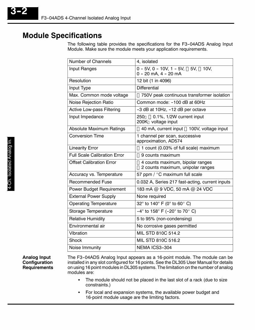
F3--0
4AD
S4-
Ch.
Isol
ated
Ana
log
In.
3--2F3--04ADS 4-Channel Isolated Analog Input
Module SpecificationsThe following table provides the specifications for the F3--04ADS Analog InputModule. Make sure the module meets your application requirements.
Number of Channels 4, isolated
Input Ranges 0 -- 5V, 0 -- 10V, 1 -- 5V, ? 5V, ? 10V,0 -- 20 mA, 4 -- 20 mA
Resolution 12 bit (1 in 4096)
Input Type Differential
Max. Common mode voltage ? 750V peak continuous transformer isolation
Noise Rejection Ratio Common mode: --100 dB at 60Hz
Active Low-pass Filtering --3 dB at 10Hz, --12 dB per octave
Input Impedance 250O ? 0.1%, 1/2W current input200KO voltage input
Absolute Maximum Ratings ? 40 mA, current input ? 100V, voltage input
Conversion Time 1 channel per scan, successiveapproximation, AD574
Linearity Error ? 1 count (0.03% of full scale) maximum
Full Scale Calibration Error ? 9 counts maximum
Offset Calibration Error ? 4 counts maximum, bipolar ranges? 2 counts maximum, unipolar ranges
Accuracy vs. Temperature 57 ppm / _C maximum full scale
Recommended Fuse 0.032 A, Series 217 fast-acting, current inputs
Power Budget Requirement 183 mA @ 9 VDC, 50 mA @ 24 VDC
External Power Supply None required
Operating Temperature 32° to 140° F (0° to 60_ C)
Storage Temperature --4° to 158° F (--20° to 70_ C)
Relative Humidity 5 to 95% (non-condensing)
Environmental air No corrosive gases permitted
Vibration MIL STD 810C 514.2
Shock MIL STD 810C 516.2
Noise Immunity NEMA ICS3--304
The F3--04ADS Analog Input appears as a 16-point module. The module can beinstalled in any slot configured for 16 points. See the DL305 User Manual for detailson using 16 point modules in DL305 systems. The limitation on the number of analogmodules are:
S The module should not be placed in the last slot of a rack (due to sizeconstraints.)
S For local and expansion systems, the available power budget and16-point module usage are the limiting factors.
Analog InputConfigurationRequirements

F3--04AD
S4-C
h.IsolatedA
nalogIn.
3--3F3--04ADS 4-Channel Isolated Analog Input
Setting the Module Jumpers
The module is set at the factory for a 4--20 mA signal on all four channels. If this isacceptable you do not have to change any of the jumpers. The following diagramshows how the jumpers are set.
Channel 1
J10
UNIPOLAR BIPOLAR
Pin 1
If you examine the rear of the module, you’llnotice several jumpers. The jumpers labeled +1and +2 (located on the larger board, near theterminal block) are used to select the number ofchannels that will be used.Without any jumpers the module processes onechannel. By installing the jumpers you can addchannels. The module is set from the factory forfour channel operation.For example, if you install the +1 jumper, youadd one channel for a total of two. Now if youinstall the +2 jumper you add two more channelsfor a total of four.Any unused channels are not processed so ifyou only select channels 1, 2, and 3, channel 4will not be active. The table shows whichjumpers to install.
+1
+2
Jumpers installed as shownselects 4-channel operation
Channel +1 +21 No No1, 2, Yes No1, 2, 3 No Yes1, 2, 3, 4 Yes Yes
Jumper Locations
Selecting theNumber ofChannels

F3--0
4AD
S4-
Ch.
Isol
ated
Ana
log
In.
3--4F3--04ADS 4-Channel Isolated Analog Input
As you examin the jumper settings, notice there are jumpers for each individualchannel. These jumpers allow you to select the type of signal (voltage or current) andthe range of the signal. The following tables show the jumper selections for thevarious ranges. Only channel 1 is used in the example, but all channels must be set.
NOTE: The Polarity jumper selects Unipolar or Bipolar operation for all channels.
Bipolar Signal Range Jumper Settings
--5 VDC to +5 VDC
(--20 to +20 mA)
--10 VDC to +10 VDC
Unipolar Signal Range Jumper Settings
4 to 20 mA
(1 VDC to 5 VDC, remove the cur-rent jumper)
0 VDC to +5 VDC
(0 to +20 mA, install the currentjumper)
0 VDC to +10 VDC
Selecting InputSignal Ranges
1
PolarityUni Bi
Channel 1 Ranges Current Jumper
1
PolarityUni Bi
Channel 1 Ranges Current Jumper
1
PolarityUni Bi
Channel 1 Ranges Current Jumper
1
PolarityUni Bi
Channel 1 Ranges Current Jumper
1
PolarityUni Bi
Channel 1 Ranges Current Jumper

F3--04AD
S4-C
h.IsolatedA
nalogIn.
3--5F3--04ADS 4-Channel Isolated Analog Input
Connecting the Field Wiring
Your company may have guidelines for wiring and cable installation. If so, you shouldcheck those before you begin the installation. Here are some general things toconsider.
S Use the shortest wiring route whenever possible.S Use shielded wiring and ground the shield at the signal source. Do not
ground the shield at both the module and the source.S Do not run the signal wiring next to large motors, high current switches,
or transformers. This may cause noise problems.S Route the wiring through an approved cable housing to minimize the risk
of accidental damage. Check local and national codes to choose thecorrect method for your application.
The F3--04ADS receives all power from the base. A separate power supply is notrequired.Occasionally you may have the need to connect a transmitter with an unusual signalrange. By changing the wiring slightly and adding an external resistor to convert thecurrent to voltage, you can easily adapt this module to meet the specifications for atransmitter which does not adhere to one of the standard input ranges. The followingdiagram shows how this works.
R =Vmax
Imax
R = value of external resistorVmax = high limit of selected voltage rangeImax = maximum current supplied by the transmitter
Example: current transmitter capable of 50mA, 0 -- 10V range selected.
R =10V
50mA
R = 200 ohms
Internal
+CH1
--CH1
+
--250O
R
JumperRemoved
ModuleCircuitry
50mACurrent
Transmitter
+
--
NOTE: Your choice of resistor can affect the accuracy of the module. A resistor witha ? 0.1% tolerance and a ? 50ppm / _C temperature coefficient is recommended.
Wiring Guidelines
User Power SupplyRequirementsCustom InputRanges

F3--0
4AD
S4-
Ch.
Isol
ated
Ana
log
In.
3--6F3--04ADS 4-Channel Isolated Analog Input
Standard 4 to 20 mA transmitters and transducers can operate from a wide variety ofpower supplies. Not all transmitters are alike and the manufacturers often specify aminimum loop or load resistance that must be used with the transmitter.The F3--04ADS provides 250 ohm resistance for each channel. If your transmitterrequires a load resistance below 250 ohms, then you do not have to make anyadjustments. However, if your transmitter requires a load resistance higher than 250ohms, then you need to add a resistor in series with the module.Consider the following example for a transmitter being operated from a 36 VDCsupply with a recommended load resistance of 750 ohms. Since the module has a250 ohm resistor, you need to add an additional resistor.
0V+36V
DC Supply
Two-wire Transmitter
+ --
R = Tr ≡ Mr R -- Resistor to addTr -- Transmitter RequirementMr -- Module resistance (internal 250 ohms)
R = 750 ≡ 250
R = 500
--+
Module Channel 1
R 250O
Current LoopTransmitterImpedance

F3--04AD
S4-C
h.IsolatedA
nalogIn.
3--7F3--04ADS 4-Channel Isolated Analog Input
The F3--04ADS module has a removable connector to make wiring easier. Simplysqueeze the top and bottom tabs and gently pull the connector from the module.
ANALOG INPUTF3--04ADS
+
--
--
+1
2
+
--
CH1
Note 1: Connect unused voltage or current inputs to 0VDCat terminal block or leave current jumper installed(see Channel 3).
Note 2: A Series 217, 0.032A, Fast-acting fuse isrecommended for 4--20mA current loops.
Note 3: Transmitters may be 2, 3, or 4 wire type.
Analog
CH3
+
--
250VoltageTransmitter
+
--
CH2Voltage
Transmitter
+
--
CH44--20mACurrent
Transmitter
J10
250 J11
250 J13
250 J14
JumperInstalled
CH4 JumperInstalled
+
--
+
--
+
--
Circuitry
to
AnalogCircuitry
to
AnalogCircuitry
to
AnalogCircuitry
to
See Notes
Note 4: Transmitters may be powered from separatepower sources.
Note 5: Terminate all shields of the cable at their respectivesignal source.
CH3Not Used
Internal Module Wiring
+
--
--
+3
4
RemovableConnector
Wiring Diagram

F3--0
4AD
S4-
Ch.
Isol
ated
Ana
log
In.
3--8F3--04ADS 4-Channel Isolated Analog Input
Module Operation
Before you begin writing the control program, it is important to take a few minutes tounderstand how the module processes and represents the analog signals.The F3--04ADS module supplies1 channel of data per each CPU scan. Since thereare four channels, it can take up to four scans to get data for all channels. Once allchannels have been scanned the process starts over with channel 1.You do not have to select all of the channels. Unused channels are not processed, soif you select only two channels, then each channel will be updated every other scan.
Channel 1 Scan N
Read the data
Store data
I/O Update
Execute Application ProgramChannel 2 Scan N+1
Channel 3 Scan N+2
Channel 4 Scan N+3
Channel 1 Scan N+4
Scan
Even though the channel updates to the CPU are synchronous with the CPU scan,the module asynchronously monitors the analog transmitter signal and converts thesignal to a 12-bit binary representation. This enables the module to continuouslyprovide accurate measurements without slowing down the discrete control logic inthe RLL program.
Channel ScanningSequence

F3--04AD
S4-C
h.IsolatedA
nalogIn.
3--9F3--04ADS 4-Channel Isolated Analog Input
You may recall the F3--04ADS module appears to the CPU as a 16-point module.These 16 points provide:
S an indication of which channel is active.S the digital representation of the analog signal.
Since all I/O points are automatically mapped into Register (R) memory, it is veryeasy to determine the location of the data word that will be assigned to the module.
110
F3--04ADS
R 011MSB LSB
R 001MSB LSB
010
R 002, R012 R 000, R010
117
8ptRelay
8ptOutput
16ptInput
16pt(Analog)
4ch.Input
8ptOutput
050--
057
040--
047
030--
037
020027
--120127
000007
--100107
010017
--110117
017
Within these two register locations, the individual bits represent specific informationabout the analog signal.
The last four points of the upper registerare used as inputs to tell the CPU whichchannel is being processed. In ourexample, when input 114 is on themodule is telling the CPU it is processingchannel 1. Here’s how the inputs areassigned.Input Active Channel114 1115 2116 3117 4
R011MSB LSB
110
117
116
115
114
113
112
111
-- channel selection inputs
Understanding theI/O Assignments
Active ChannelSelection Inputs

F3--0
4AD
S4-
Ch.
Isol
ated
Ana
log
In.
3--10F3--04ADS 4-Channel Isolated Analog Input
The remaining twelve bits represent theanalog data in binary format.Bit Value Bit Value0 (LSB) 1 6 641 2 7 1282 4 8 2563 8 9 5124 16 10 10245 32 11 2048
117
R001MSB LSB
010
116
115
114
113
112
111
110
017
016
015
014
013
012
011
-- data bits
R011
Since the module has 12-bit resolution, the analog signal is converted into 4096“pieces” ranging from 0 -- 4095 (212). For example, with a 0 to 10V scale, a 0V signalwould be 0, and a 10V signal would be 4095. This is equivalent to a a binary value of0000 0000 0000 to 1111 1111 1111, or 000 to FFF hexadecimal. The followingdiagram shows how this relates to each signal range.
+V
0V
--V0 4095
--10V -- +10V--5V -- +5V
+V
0V0 4095
0V -- 10V0V -- 5V
+5V
1V
0 4095
1V -- 5V
20mA
4mA
0 4095
4 -- 20mA
Each “piece” can also be expressed interms of the signal level by using theequation shown. The following tableshows the smallest signal levels that willresult in a change in the data value foreach signal range.
Resolution = H ≡ L4095
H = high limit of the signal rangeL = low limit of the signal range
Range Highest Signal Lowest Signal Smallest Change
--10 to +10V +10V --10V 4.88 mV
--5 to +5V +5 V --5V 2.44 mV
0 to 5V 5V 0V 1.22 mV
0 to 10V 10 V 0V 2.44 mV
1 to 5V 5V 1V 0.98 mV
4 to 20mA 20mA 4mA 3.91 µA
Now that you understand how the module and CPU work together to gather andstore the information, you’re ready to write the control program.
Analog Data Bits

F3--04AD
S4-C
h.IsolatedA
nalogIn.
3--11F3--04ADS 4-Channel Isolated Analog Input
Writing the Control Program
Since all channels are multiplexed into a single data word, the control program mustbe setup to determine which channel is being read. Since the module provides inputpoints to the CPU, it is very easy to use the active channel status bits to determinewhich channel is being monitored.
110
F3--04ADS
R 011MSB LSB
R 001MSB LSB
010
R 002, R012 R 000, R010
117
8ptRelay
8ptOutput
16ptInput
16pt(Analog)
4ch.Input
8ptOutput
050--
057
040--
047
030--
037
020027
--120127
000007
--100107
010017
--110117
017
The following example shows a program that is designed to read a single channel ofanalog data into a Register location on every scan. Once the data is in a Register,you can perform math on the data, compare the data against preset values, etc. Thisexample is designed to read channel 1. Since you use jumpers to select the numberof channels to scan, this is the only channel that you can use in this manner.
374DSTR1R001
F51
Read the data
This rung loads the data into the accumulator onevery scan. (You can use any permissive contact.)
BCD F86
114DOUTR400
F60
Store channel 1The active channel inputs are used to let the CPUknow which channel has been loaded into theaccumulator. (Since you cannot isolate theindividual channels for scanning, channel 1 is theonly channel that can be used in this manner.) Byusing the input to control a DOUT instruction, youcan easily move the data to a storage register. TheBCD value will be stored in R400 and R401. (Twobytes are required for four digit BCD numbers.)
The DL305 CPUs perform math operations inBCD. This instruction converts the binary data toBCD. (You can omit this step if your applicationdoes not require the conversion.)
Identifying theData Locations
Single Channel onEvery Scan

F3--0
4AD
S4-
Ch.
Isol
ated
Ana
log
In.
3--12F3--04ADS 4-Channel Isolated Analog Input
The following example shows a program designed to read any of the availablechannels of analog data into Register locations. Once the data is in a Register, youcan perform math on the data, compare the data against preset values, etc. Sincethe DL305 CPUs use 8-bit word instructions, you have to move the data in pieces. It’ssimple if you follow the example.
374DSTR3R011
F53
Read the data
This rung loads the four most significant data bitsinto the accumulator from Register 011. (A normallyclosed 374 means it is loaded on every scan.)
DOUT1R501
F61
114DOUTR400
F60
Store channel 1
115DOUTR402
F60
Store channel 2
116DOUTR404
F60
Store channel 3
117DOUTR406
F60
Store channel 4
The channel selection inputs are used to let theCPU know which channel has been loaded into theaccumulator. By using these inputs to control aDOUT instruction, you can easily move the data toa storage register. Notice the DOUT instructionstores the data in two bytes. (Two bytes arerequired for four digit BCD numbers.)
Temporarily store the bits to Register 501.
DSTR1R001
F51 This rung loads the eight least significant data bitsinto the accumulator from Register 001.
DOUT1R500
F61 Temporarily store the bits to Register 500. Sincethe most significant bits were loaded into 501, nowR500 and R501 contain all twelve bits in order.
DSTRR500
F50
BCD F86
Now that all the bits are stored, load all twelve bitsinto the accumulator.
Math operations are performed in BCD. Thisinstruction converts the binary data to BCD. (Youcan omit this step if your application does notrequire the conversion.)
Reading MultipleChannels overAlternating Scans

F3--04AD
S4-C
h.IsolatedA
nalogIn.
3--13F3--04ADS 4-Channel Isolated Analog Input
The example below shows how to scale input data from an F3--04ADS Analogmodule in the X0 position of the D3--XX--1 base. This module must be placed in a 16bit slot in order to work.
This writes channel one analog data to V2000when X14 (channel select 1) is on.
OUTX14
_On
LDF
K12
X0This rung loads the first twelve bits of data from X0and then converts it to BCD format.
Load the data
SP1
BCD
V2000
Channel 1 Select Bit
OUTX15
V2001
Channel 2 Select Bit
This writes channel two analog data to V2001when X15 (channel select 2) is on.
OUTX16
V2002
Channel 3 Select Bit
This writes channel three analog data to V2002when X16 (channel select 3) is on.
OUTX17
V2003
Channel 4 Select Bit
This writes channel four analog data to V2003when X17 (channel select 4) is on.
The example below shows how to read multiple channels on an F3--04ADS Analogmodule in the 20--27/120--127 address slot. This module must be placed in a 16 bitslot in order to work.
This writes channel one analog data to V3000when the Channel 1 Select Bit (X124) is set.
OUT
_On
LDF
K8
X120This rung loads the upper byte of analog data fromthe module.
Load the data
SP1
BCD
V3000
Channel 1 Select Bit
SHFL
ANDD
ORF
K8
X20
K8
Kfff
The ORF X20 brings the lower byte of data fromthe module into the accumulator. At this time thereis a full word of data from the analog module in theaccumulator.
SHFL K8 shifts the data to the left eight places tomake room for the lower byte of data.
The ANDD Kfff masks off the twelve leastsignificant bits of data from the word. This is theactual analog value.
The BCD command converts the data to BCDformat.
X124
Reading MultipleChannels overAlternating Scanson a DL350 with aD3--XX--1 Base
Reading MultipleChannels overAlternating Scanson a DL350 with aConventional Base

F3--0
4AD
S4-
Ch.
Isol
ated
Ana
log
In.
3--14F3--04ADS 4-Channel Isolated Analog Input
Most applications usually requiremeasurements in engineering units,which provide more meaningful data.This is accomplished by using theconversion formula shown.
Units = A4096 S
Units = value in Engineering UnitsA = Analog value (0 -- 4095)S = high limit of the Engineeringunit range
The following example shows how youwould use the analog data to representpressure (PSI) from 0 to 100. Thisexample assumes the analog value is1760. This should yield approximately42.9 PSI.
Units = 17604096
100
Units = A4096 S
Units = 42.9
Scaling the InputData

F3--04AD
S4-C
h.IsolatedA
nalogIn.
3--15F3--04ADS 4-Channel Isolated Analog Input
The following instructions are required to scale the data. We’ll continue to use the42.9 PSI example. In this example we’re using channel 1. Input 114 is the activechannel indicator for channel 1. Of course, if you were using a different channel, youwould use the active channel indicator point that corresponds to the channel youwere using.
114DSTRR400
F50
DIVK4096
F74
This instruction brings the analog value (in BCD)into the accumulator.
This instruction moves the two-byte decimalportion into the accumulator for further operations.
Scale the data
The analog value is divided by the resolution of themodule, which is 4096. (1760 / 4096 = 0.4296)
DSTRR576
F50
MULK100
F73
DSTRR576
F50
DOUTR450
F60
1 7 6 0Accumulator
0 0 0 0Aux. Accumulator
0 0 0 0Accumulator
4 2 9 6Aux. Accumulator
This example assumes you have already read the analog dataand stored the BCD equivalent in R400 and R401
4 2 9 6Accumulator
4 2 9 6Aux. Accumulator
The accumulator is then multiplied by the scalingfactor, which is 100. (100 x 4296 = 429600). Noticethe most significant digits are now stored in theauxilliary accumulator. (This is different from theway the Divide instruction operates.)
9 6 0 0Accumulator
0 0 4 2Aux. Accumulator
R577 R576
R577 R576
R577 R576
R577 R576
This instruction moves the two-byte auxilliaryaccumulator for further operations.
0 0 4 2Accumulator
0 0 4 2Aux. Accumulator
R577 R576
This instruction stores the accumulator to R450.R450 now contains the PSI, which is 42 PSI.
0 0 4 2Accumulator
0 0 4 2Store in R451 & R450
R451 R450

F3--0
4AD
S4-
Ch.
Isol
ated
Ana
log
In.
3--16F3--04ADS 4-Channel Isolated Analog Input
You probably noticed the previous example yielded 42 PSI when the real valueshould have been 42.9 PSI. By changing the scaling value slightly, we can “imply” anextra decimal of precision. Notice in the following example we’ve added another digitto the scale. Instead of a scale of 100, we’re using 1000, which implies 100.0 for thePSI range.
114DSTRR400
F50
DIVK4096
F74
This instruction brings the analog value (in BCD)into the accumulator.
This instruction moves the two-byte decimalportion into the accumulator for further operations.
Scale the data
The analog value is divided by the resolution of themodule, which is 4096. (1760 / 4096 = 0.4296)
DSTRR576
F50
MULK1000
F73
DSTRR576
F50
DOUTR450
F60
1 7 6 0Accumulator
0 0 0 0Aux. Accumulator
0 0 0 0Accumulator
4 2 9 6Aux. Accumulator
This example assumes you have already read the analog dataand stored the BCD equivalent in R400 and R401
4 2 9 6Accumulator
4 2 9 6Aux. Accumulator
The accumulator is multiplied by the scaling factor,which is now 1000. (1000 x 4296 = 4296000). Themost significant digits are now stored in theauxilliary accumulator. (This is different from theway the Divide instruction operates.)
6 0 0 0Accumulator
0 4 2 9Aux. Accumulator
R577 R576
R577 R576
R577 R576
R577 R576
This instruction moves the two-byte auxilliaryaccumulator for further operations.
0 4 2 9Accumulator
0 4 2 9Aux. Accumulator
R577 R576
This instruction stores the accumulator to R450and R451. R450 and R451 now contain the PSI,which implies 42.9.
0 4 2 9Accumulator
0 4 2 9Store in R451 & R450
R451 R450

F3--04AD
S4-C
h.IsolatedA
nalogIn.
3--17F3--04ADS 4-Channel Isolated Analog Input
This example program shows how you can use the instructions to load theseequation constants into data registers. The example is written for channel 1, but youcan easily use a similar approach to use different scales for all channels if required.You may just use the appropriate constants in the instructions dedicated for eachchannel, but this method allows easier modifications. For example, you could easilyuse an operator interface or a programming device to change the constants if theyare stored in Registers.
This rung loads the four most significant data bitsinto the accumulator from Register 011.
Temporarily store the bits to Register 501.
DSTR3R011
F53
DOUT1R501
F61
374Read the data
114Store channel 1
374DSTRK4096
F50
DOUTR430
F60
DSTRK1000
F50
DOUTR432
F60
On the first scan, these first two instructions loadthe analog resolution (constant of 4096) into R430and R431.
These two instructions load the high limit of theEngineering unit scale (constant of 1000) intoR432 and R433. Note, if you have different scalesfor each channel, you’ll also have to enter theEngineering unit high limit for those as well.
Load the constants
DIVR430
F74
DSTRR576
F50
MULR432
F73
This instruction moves the decimal portion from theauxilliary accumulator into the regular accumulatorfor further operations.
The analog value is divided by the resolution of themodule, which is stored in R430.
DSTRR576
F50
DOUTR400
F60
The accumulator is multiplied by the scaling factor,which is stored in R432.
This instruction moves most significant digits (nowstored in the auxilliary accumulator) into theregular accumulator for further operations.
The scaled value is stored in R400 and R401 forfurther use.

F3--0
4AD
S4-
Ch.
Isol
ated
Ana
log
In.
3--18F3--04ADS 4-Channel Isolated Analog Input
The example below shows how to scale input data from an F3--04ADS Analogmodule in the 20--27/120--127 address slot. This module must be placed in a 16 bitslot in order to work.
X125 is the channel select bit for channel two. Thisrung puts the data from the analog module into therespective V--memory location.
OUTChannel 2
X125
_On
LDF
K8
X120
SHFL K8
ORF
K8
X20
ANDD Kfff
This loads the upper byte of the analog data fromthe module.
The ORF X20 brings the lower byte of data fromthe module into the accumulator. At this time thereis a full word of data from the analog module in theaccumulator.
Load the data
MUL K1800
Rung 3 scales a 0 to 180 range of a transducerover the 4096 counts. The raw analog value isloaded to the accumulator from V3001(Channel #2).
DIV K4096
OUT V3010
It is then multiplied by 1800. The additional zeroprovides a higher degree of resolution.
It is then divided by 4096, which is the resolution ofthe module.
The scaled value is stored in V3010 with animplied decimal.
SP1
SHFL K8 shifts the data to the left eight places tomake room for the lower byte of data.
BCD
The ANDD Kfff masks off the twelve leastsignificant bits of data from the word. This is theactual analog value.
The BCD command converts the data to BCDformat.
Analog DataRegister (BCD)
V3001
Channel 2 Select Bit
_OnSP1 LD
Channel 2Analog DataRegister (BCD)
V3001
Select Channel 2
Scale the data
Scaling on a DL350with aConventionalDL305 Base

F3--04AD
S4-C
h.IsolatedA
nalogIn.
3--19F3--04ADS 4-Channel Isolated Analog Input
Sometimes it is helpful to be able to quickly convert between the signal levels and thedigital values. This is especially helpful during machine startup or troubleshooting.The following table provides formulas to make this conversion easier.
Range If you know the digital value ... If you know the analog signallevel ...
--10V to + 10V
--5V to + 5V
0 to 5V
0 to 10V
1 to 5V
4 to 20mA
For example, if you are using the --10 to+10V range and you have measured thesignal at 6V, you would use the followingformula to determine the digital valuethat should be stored in the registerlocation that contains the data.
D = 409520
(A + 10)
D = 409520
(6V + 10)
D = (204.75) (16)
D = 3276
Now you have all the necessary information to get your analog module installed andoperating correctly!
Analog and DigitalValue Conversions
A = 20D4095 ≡ 10 D = 4095
20(A + 10)
A = 10D4095 ≡ 5 D = 4095
10(A + 5)
A = 5D4095 D = 4095
5A
A = 10D4095 D = 4095
10A
A = 4D4095 + 1 D = 4095
4(A ≡ 1)
A = 16D4095 + 4 D = 4095
16(A ≡ 4)

14F3--08AD8-ChannelAnalog Input
In This Chapter. . . .— Module Specifications— Setting the Module Jumpers— Connecting the Field Wiring— Module Operation— Writing the Control Program

F3--0
8AD
8-C
hann
elA
nalo
gIn
put
4--2F3--08AD 8-Channel Analog Input
Module Specifications
The following table provides the specifications for the F3--08AD Analog InputModule from FACTS Engineering. Review these specifications to make sure themodule meets your application requirements.
Number of Channels 8, single ended (one common)
Input Ranges 4 -- 20 mA
Resolution 12 bit (1 in 4096)
Input Impedance 250O ? 0.1%, 1/2W current input
Absolute Maximum Ratings ? 30mA
Conversion Time 35µs per channel1 channel per CPU scan
Converter Type Successive Approximation, AD574
Linearity Error ? 1 count (0.03% of full scale) maximum
Maximum Inaccuracy 0.35% of full scale at 77 °F (25 °C)
Accuracy vs. Temperature 57 ppm / _C maximum full scale (includingmaximum offset change of 2 counts)
Recommended Fuse 0.032 A, Series 217 fast-acting
Power Budget Requirement 25 mA @ 9 VDC, 37 mA @ 24 VDC
External Power Supply None required
Operating Temperature 32° to 140° F (0° to 60_ C)
Storage Temperature --4° to 158° F (--20° to 70_ C)
Relative Humidity 5 to 95% (non-condensing)
Environmental air No corrosive gases permitted
Vibration MIL STD 810C 514.2
Shock MIL STD 810C 516.2
Noise Immunity NEMA ICS3--304
The F3--08AD Analog Input appears as a 16-point module. The module can beinstalled in any slot configured for 16 points. See the DL305 User Manual for detailson using 16 point modules in DL305 systems. The limitation on the number of analogmodules are:
S For local and expansion systems, the available power budget and16-point module usage are the limiting factors.
Analog InputConfigurationRequirements

F3--08AD
8-ChannelA
nalogInput
4--3F3--08AD 8-Channel Analog Input
Setting the Module Jumpers
The module is set at the factory for a 4--20 mA signal on all eight channels. If this isacceptable you do not have to change any of the jumpers. The following diagramshows how the jumpers are set.
Channels+1
+2+4
If you examine the rear of the module,you’ll notice several jumpers. Thejumpers labeled +1, +2 and +4 are usedto select the number of channels that willbe used. Without any jumpers themodule processes one channel (channel1). By installing the jumpers you can addchannels. The module is set from thefactory for eight channel operation.For example, if you install the +1 jumper,you add one channel for a total of two.Now if you install the +2 jumper you addtwo more channels for a total of four.Any unused channels are not processedso if you only select channels 1--4, thenthe last four channels will not be active.The following table shows which jumpersto install.Channel(s) +4 +2 +11 No No No1 2 No No Yes1 2 3 No Yes No1 2 3 4 No Yes Yes1 2 3 4 5 Yes No No1 2 3 4 5 6 Yes No Yes1 2 3 4 5 6 7 Yes Yes No1 2 3 4 5 6 7 8 Yes Yes Yes
Jumpers installed as shownselects 8-channel operation
+4 +2 +1
Number ofChannels
Jumper Locations
Selecting theNumber ofChannels

F3--0
8AD
8-C
hann
elA
nalo
gIn
put
4--4F3--08AD 8-Channel Analog Input
Connecting the Field Wiring
Your company may have guidelines for wiring and cable installation. If so, you shouldcheck those before you begin the installation. Here are some general things toconsider.
S Use the shortest wiring route whenever possible.S Use shielded wiring and ground the shield at the signal source. Do not
ground the shield at both the module and the source.S Don’t run the signal wiring next to large motors, high current switches, or
transformers. This may cause noise problems.S Route the wiring through an approved cable housing to minimize the risk
of accidental damage. Check local and national codes to choose thecorrect method for your application.
The F3--08AD receives all power from the base. A separate power supply is notrequired.
Standard 4 to 20 mA transmitters and transducers can operate from a wide variety ofpower supplies. Not all transmitters are alike and the manufacturers often specify aminimum loop or load resistance that must be used with the transmitter.The F3--08AD provides 250 ohm resistance for each channel. If your transmitterrequires a load resistance below 250 ohms, then you do not have to make anyadjustments. However, if your transmitter requires a load resistance higher than 250ohms, then you need to add a resistor in series with the module.Consider the following example for a transmitter being operated from a 36 VDCsupply with a recommended load resistance of 750 ohms. Since the module has a250 ohm resistor, you need to add an additional resistor.
0V+36V
DC Supply
Two-wire Transmitter
+ --
R = Tr ≡ Mr R -- Resistor to addTr -- Transmitter RequirementMr -- Module resistance (internal 250 ohms)
R = 750 ≡ 250
R = 500
--+
Module Channel 1
R 250O
Wiring Guidelines
User Power SupplyRequirements
Current LoopTransmitterImpedance

F3--08AD
8-ChannelA
nalogInput
4--5F3--08AD 8-Channel Analog Input
The F3--08AD module has a removable connector to make wiring easier. Simplysqueeze the top and bottom tabs and gently pull the connector from the module.
Internal Module Wiring
1+
2+
1--
2--
3+
4+
3--
4--
5+
6+
5--
6--
7+
8+
7--
8--
COM
ANALOG INPUTF3--08AD
COM
+4--
+2--
+6--
+8--
+3--
+1--
+5--
+7--
COM
4--20mAA/D
Note 1: Terminate all shields at their respective signal source
Note 2: To avoid “ground loop” errors, the following transmittertypes are recommended:
2 & 3 wire: Isolation between input signal & P/S4 wire: Full isolation between input signal, P/S andoutput signal.
+ --
250
4 wire 4--20mATransmitter P/S
4 wire4--20mA
3 wire4--20mA
2 wire4--20mA
3 wire4--20mA
2 wire4--20mA
4 wire4--20mA
4 wire4--20mA
4 wire4--20mA
+
--
External P/Sfor 4--20mATransmitters
(Switching Type DC P/S not recommended)
1+
2+
1--
2--
3+
4+
3--
4--
5+
6+
5--
6--
7+
8+
7--
8--
COM
COM
250
250
250
250
250
250
250
AnalogSwitch
See note
RemovableConnector
Wiring Diagram

F3--0
8AD
8-C
hann
elA
nalo
gIn
put
4--6F3--08AD 8-Channel Analog Input
Module Operation
Before you begin writing the control program, it is important to take a few minutes tounderstand how the module processes and represents the analog signals.The F3--08AD module supplies1 channel of data per each CPU scan. Since thereare eight channels, it can take up to eight scans to get data for all channels. Once allchannels have been scanned the process starts over with channel 1.You do not have to select all of the channels. Unused channels are not processed, soif you select only four channels, then the channels will be updated within four scans.
I/O Update
Channel 1 Scan N
Read the data
Store data
Execute Application ProgramChannel 2 Scan N+1
Channel 8 Scan N+7
Channel 1 Scan N+8
Scan
.
.
.
.
.
.
Even though the channel updates to the CPU are synchronous with the CPU scan,the module asynchronously monitors the analog transmitter signal and converts thesignal to a 12-bit binary representation. This enables the module to continuouslyprovide accurate measurements without slowing down the discrete control logic inthe RLL program.
Channel ScanningSequence
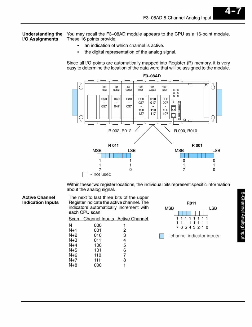
F3--08AD
8-ChannelA
nalogInput
4--7F3--08AD 8-Channel Analog Input
You may recall the F3--08AD module appears to the CPU as a 16-point module.These 16 points provide:
S an indication of which channel is active.S the digital representation of the analog signal.
Since all I/O points are automatically mapped into Register (R) memory, it is veryeasy to determine the location of the data word that will be assigned to the module.
110
F3--08AD
R 011MSB LSB
R 001MSB LSB
010
R 002, R012 R 000, R010
117
8ptRelay
8ptOutput
16ptInput
16pt(Analog)
8chInput
8ptOutput
050--
057
040--
047
030--
037
020027
--120127
000007
--100107
010017
--110117
017
-- not used
Within these two register locations, the individual bits represent specific informationabout the analog signal.
The next to last three bits of the upperRegister indicate the active channel. Theindicators automatically increment witheach CPU scan.Scan Channel Inputs Active ChannelN 000 1N+1 001 2N+2 010 3N+3 011 4N+4 100 5N+5 101 6N+6 110 7N+7 111 8N+8 000 1
R011MSB LSB
110
117
116
115
114
113
112
111
-- channel indicator inputs
Understanding theI/O Assignments
Active ChannelIndication Inputs

F3--0
8AD
8-C
hann
elA
nalo
gIn
put
4--8F3--08AD 8-Channel Analog Input
The remaining twelve bits represent theanalog data in binary format.Bit Value Bit Value0 (LSB) 1 6 641 2 7 1282 4 8 2563 8 9 5124 16 10 10245 32 11 2048
117
R001MSB LSB
010
116
115
114
113
112
111
110
017
016
015
014
013
012
011
-- data bits
R011
Since the module has 12-bit resolution,the analog signal is converted into 4096“pieces” ranging from 0 -- 4095 (212). Forexample, with a 4 -- 20 mA scale, a 4 mAsignal would be 0, and a 20 mA signalwould be 4095. This is equivalent to abinary value of 0000 0000 0000 to1111 1111 1111, or 000 to FFFhexadecimal. The following diagramshows how this relates to each signalrange.Each “piece” can also be expressed interms of the signal level by using theequation shown. The following tableshows the smallest signal levels that willresult in a change in the data value foreach signal range.
20mA
4mA
0 4095
4 -- 20mA
Resolution = H ≡ L4095
H = high limit of the signal rangeL = low limit of the signal range
Range Highest Signal Lowest Signal Smallest Change
4 to 20mA 20mA 4mA 3.91 µA
Now that you understand how the module and CPU work together to gather andstore the information, you’re ready to write the control program.
Analog Data Bits

F3--08AD
8-ChannelA
nalogInput
4--9F3--08AD 8-Channel Analog Input
Writing the Control Program
Since all channels are multiplexed into a single data word, the control program mustbe setup to determine which channel is being read. Since the module provides inputpoints to the CPU, it is very easy to use the active channel status bits to determinewhich channel is being monitored.
110
F3--08AD
R 011MSB LSB
R 001MSB LSB
010
R 002, R012 R 000, R010
117
8ptRelay
8ptOutput
16ptInput
16pt(Analog)
8chInput
8ptOutput
050--
057
040--
047
030--
037
020027
--120127
000007
--100107
010017
--110117
017
-- not used
The following example shows a program that is designed to read a single channel ofanalog data into a Register location on every scan. Once the data is in a Register,you can perform math on the data, compare the data against preset values, etc. Thisexample is designed to read channel 1. Since you use jumpers to select the numberof channels to scan, this is the only channel that you can use in this manner.
374DSTR1R001
F51
Read the data
This rung loads the data into the accumulator onevery scan. (You can use any permissive contact.)
BCD F86
DOUTR400
F60 Since the active channel indicators are all off whenchannel 1 is being read, you would not have to usethem. (Since you cannot isolate the individualchannels for scanning, channel 1 is the onlychannel that can be used in this manner.) TheDOUT instruction moves the data to a storageregister. The BCD value will be stored in R400 andR401. (Two bytes are required for four digit BCDnumbers.)
The DL305 CPUs perform math operations inBCD. This instruction converts the binary data toBCD. (You can omit this step if your applicationdoes not require the conversion.)
Identifying theData Locations
Single Channel onEvery Scan

F3--0
8AD
8-C
hann
elA
nalo
gIn
put
4--10F3--08AD 8-Channel Analog Input
The following example shows a program designed to read any of the availablechannels of analog data into Register locations. Once the data is in a Register, youcan perform math on the data, compare the data against preset values, etc. Sincethe DL305 CPUs use 8-bit word instructions, you have to move the data in pieces. It’ssimple if you follow the example.
374DSTR3R011
F53
Read the data
This rung loads the four most significant data bitsinto the accumulator from Register 011 on everyscan. (You could use any permissive contact.)
DOUT1R501
F61
114DOUTR400
F60
Store channel 1
DOUTR402
F60
Store channel 2
DOUTR404
F60
Store channel 3
The channel indicator inputs are used to let theCPU know which channel has been loaded into theaccumulator. By using these inputs to control aDOUT instruction, you can easily move the data toa storage register. Notice the DOUT instructionstores the data in two bytes. (Two bytes arerequired for four digit BCD numbers.)
Temporarily store the bits to Register 501.
DSTR1R001
F51 This rung loads the eight least significant data bitsinto the accumulator from Register 001.
DOUT1R500
F61 Temporarily store the bits to Register 500. Sincethe most significant bits were loaded into 501, nowR500 and R501 contain all twelve bits in order.
DSTRR500
F50
BCD F86
Now that all the bits are stored, load all twelve bitsinto the accumulator.
Math operations are performed in BCD. Thisinstruction converts the binary data to BCD. (Youcan omit this step if your application does notrequire the conversion.)
115 116
114 115 116
114 115 116
114DOUTR406
F60
Store channel 4
DOUTR410
F60
Store channel 5
DOUTR412
F60
Store channel 6
115 116
114 115 116
114 115 116
DOUTR414
F60
Store channel 7
DOUTR416
F60
Store channel 8
114 115 116
114 115 116
Reading MultipleChannels overAlternating Scans

F3--08AD
8-ChannelA
nalogInput
4--11F3--08AD 8-Channel Analog Input
The example below shows how to read multiple channels on an F3--08AD Analogmodule in the 20--27/120--127 address slot. This module must be placed in a 16 bitslot in order to work.
This writes channel one analog data to V3000when bits X124, X125 and X126 are as shown.
OUT
_On
LDF
K8
X120This rung loads the upper byte of analog data fromthe module.
Load the data
SP1
BCD
V3000
Channel 1 Select Bit States
OUT
V3001
Channel 2 Select Bit States
OUT
V3002
Channel 3 Select Bit States
SHFL
ANDD
ORF
K8
X20
K8
Kfff
The ORF X20 brings the lower byte of data fromthe module into the accumulator. At this time thereis a full word of data from the analog module in theaccumulator.
SHFL K8 shifts the data to the left eight places tomake room for the lower byte of data.
The ANDD Kfff masks off the twelve leastsignificant bits of data from the word. This is theactual analog value.
The BCD command converts the data to BCDformat.
X125X124 X126
X125X124 X126
X125X124 X126
This writes channel two analog data to V3001when bits X124, X125 and X126 are as shown.
This writes channel three analog data to V3002when bits X124, X125 and X126 are as shown.
Reading MultipleChannels overAlternating Scanson a DL350 with aConventionalDL305 Base

F3--0
8AD
8-C
hann
elA
nalo
gIn
put
4--12F3--08AD 8-Channel Analog Input
OUT
V3003
Channel 4 Select Bit States
OUT
V3004
Channel 5 Select Bit States
OUT
V3005
Channel 6 Select Bit States
OUT
V3006
Channel 7 Select Bit States
X125X124 X126
X125X124 X126
X125X124 X126
X125X124 X126
OUT
V3007
Channel 8 Select Bit StatesX125X124 X126
This writes channel four analog data to V3003when bits X124, X125 and X126 are as shown.
This writes channel five analog data to V3004when bits X124, X125 and X126 are as shown.
This writes channel six analog data to V3005 whenbits X124, X125 and X126 are as shown.
This writes channel seven analog data to V3006when bits X124, X125 and X126 are as shown.
This writes channel eight analog data to V3007when bits X124, X125 and X126 are as shown.

F3--08AD
8-ChannelA
nalogInput
4--13F3--08AD 8-Channel Analog Input
Most applications usually requiremeasurements in engineering units,which provide more meaningful data.This is accomplished by using theconversion formula shown.
Units = A4096 S
Units = value in Engineering UnitsA = Analog value (0 -- 4095)S = high limit of the Engineeringunit range
The following example shows how youwould use the analog data to representpressure (PSI) from 0 to 100. Thisexample assumes the analog value is1760. This should yield approximately42.9 PSI.
Units = 17604096
100
Units = A4096 S
Units = 42.9
Scaling the InputData
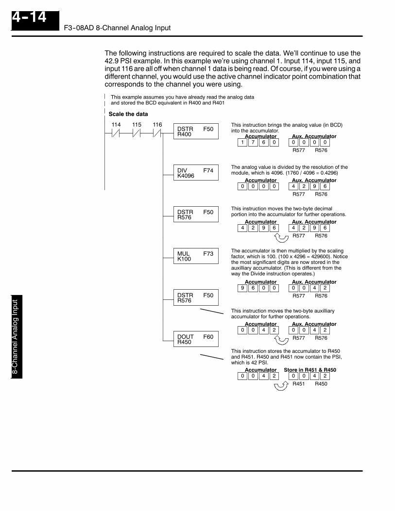
F3--0
8AD
8-C
hann
elA
nalo
gIn
put
4--14F3--08AD 8-Channel Analog Input
The following instructions are required to scale the data. We’ll continue to use the42.9 PSI example. In this example we’re using channel 1. Input 114, input 115, andinput 116 are all off when channel 1 data is being read. Of course, if you were using adifferent channel, you would use the active channel indicator point combination thatcorresponds to the channel you were using.
DSTRR400
F50
DIVK4096
F74
This instruction brings the analog value (in BCD)into the accumulator.
This instruction moves the two-byte decimalportion into the accumulator for further operations.
Scale the data
The analog value is divided by the resolution of themodule, which is 4096. (1760 / 4096 = 0.4296)
DSTRR576
F50
MULK100
F73
DSTRR576
F50
DOUTR450
F60
1 7 6 0Accumulator
0 0 0 0Aux. Accumulator
0 0 0 0Accumulator
4 2 9 6Aux. Accumulator
This example assumes you have already read the analog dataand stored the BCD equivalent in R400 and R401
4 2 9 6Accumulator
4 2 9 6Aux. Accumulator
The accumulator is then multiplied by the scalingfactor, which is 100. (100 x 4296 = 429600). Noticethe most significant digits are now stored in theauxilliary accumulator. (This is different from theway the Divide instruction operates.)
9 6 0 0Accumulator
0 0 4 2Aux. Accumulator
R577 R576
R577 R576
R577 R576
R577 R576
This instruction moves the two-byte auxilliaryaccumulator for further operations.
0 0 4 2Accumulator
0 0 4 2Aux. Accumulator
R577 R576
This instruction stores the accumulator to R450and R451. R450 and R451 now contain the PSI,which is 42 PSI.
0 0 4 2Accumulator
0 0 4 2Store in R451 & R450
R451 R450
114 115 116

F3--08AD
8-ChannelA
nalogInput
4--15F3--08AD 8-Channel Analog Input
You probably noticed the previous example yielded 42 PSI when the real valueshould have been 42.9 PSI. By changing the scaling value slightly, we can “imply” anextra decimal of precision. Notice in the following example we’ve added another digitto the scale. Instead of a scale of 100, we’re using 1000, which implies 100.0 for thePSI range.
DSTRR400
F50
DIVK4096
F74
This instruction brings the analog value (in BCD)into the accumulator.
This instruction moves the two-byte decimalportion into the accumulator for further operations.
Scale the data
The analog value is divided by the resolution of themodule, which is 4096. (1760 / 4096 = 0.4296)
DSTRR576
F50
MULK1000
F73
DSTRR576
F50
DOUTR450
F60
1 7 6 0Accumulator
0 0 0 0Aux. Accumulator
0 0 0 0Accumulator
4 2 9 6Aux. Accumulator
This example assumes you have already read the analog dataand stored the BCD equivalent in R400 and R401
4 2 9 6Accumulator
4 2 9 6Aux. Accumulator
The accumulator is multiplied by the scaling factor,which is now 1000. (1000 x 4296 = 4296000). Themost significant digits are now stored in theauxilliary accumulator. (This is different from theway the Divide instruction operates.)
6 0 0 0Accumulator
0 4 2 9Aux. Accumulator
R577 R576
R577 R576
R577 R576
R577 R576
This instruction moves the two-byte auxilliaryaccumulator for further operations.
0 4 2 9Accumulator
0 4 2 9Aux. Accumulator
R577 R576
This instruction stores the accumulator to R450and R451. R450 and R451 now contain the PSI,which implies 42.9.
0 4 2 9Accumulator
0 4 2 9Store in R451 & R450
R451 R450
114 115 116

F3--0
8AD
8-C
hann
elA
nalo
gIn
put
4--16F3--08AD 8-Channel Analog Input
This example program shows how you can use the instructions to load theseequation constants into data registers. The example was written for channel 1, butyou could easily use a similar approach to use different scales for all channels ifrequired.
You could just use the appropriate constants in the instructions dedicated for eachchannel, but this method allows easier modifications. For example, you could easilyuse an operator interface or a programming device to change the constants if theyare stored in Registers.
This rung loads the four most significant data bitsinto the accumulator from Register 011 on everyscan. (You could use any permissive contact.)
Temporarily store the bits to Register 501.
DSTR3R011
F53
DOUT1R501
F61
374Read the data
Store channel 1
374DSTRK4096
F50
DOUTR430
F60
DSTRK1000
F50
DOUTR432
F60
On the first scan, these first two instructions loadthe analog resolution (constant of 4096) into R430and R431.
These two instructions load the high limit of theEngineering unit scale (constant of 1000) intoR432 and R433. Note, if you have different scalesfor each channel, you’ll also have to enter theEngineering unit high limit for those as well.
Load the constants
DIVR430
F74
DSTRR576
F50
MULR432
F73
This instruction moves the decimal portion from theauxilliary accumulator into the regular accumulatorfor further operations.
The analog value is divided by the resolution of themodule, which is stored in R430.
DSTRR576
F50
DOUTR400
F60
The accumulator is multiplied by the scaling factor,which is stored in R432.
This instruction moves most significant digits (nowstored in the auxilliary accumulator) into theregular accumulator for further operations.
The scaled value is stored in R400 and R401 forfurther use.
114 115 116

F3--08AD
8-ChannelA
nalogInput
4--17F3--08AD 8-Channel Analog Input
The example below shows how to scale input data from an F3--08AD Analog modulein the 20--27/120--127 address slot. This module must be placed in a 16 bit slot inorder to work.
The bits X124, X125 and X126, all OFF, selectschannel one. This rung puts the data from theanalog module into the respective V--memorylocation.
OUTChannel 1
X125
_On
LDF
K8
X120
SHFL K8
ORF
K8
X20
ANDD Kfff
This loads the upper byte of the analog data fromthe module.
The ORF X20 brings the lower byte of data fromthe module into the accumulator. At this time thereis a full word of data from the analog module in theaccumulator.
Load the data
MUL K2000
Rung 3 scales a 0 to 200 range of a transducerover the 4096 counts. The raw analog value isloaded to the accumulator from V3000(Channel #1).
DIV K4096
OUT V3010
It is then multiplied by 2000. The additional zeroprovides a higher degree of resolution.
It is then divided by 4096, which is the resolution ofthe module.
The scaled value is stored in V3010 with animplied decimal.
SP1
SHFL K8 shifts the data to the left eight places tomake room for the lower byte of data.
BCD
The ANDD Kfff masks off the twelve leastsignificant bits of data from the word. This is theactual analog value.
The BCD command converts the data to BCDformat.
Analog DataRegister (BCD)
V3001
_OnSP1 LD
Channel 1Analog DataRegister (BCD)
V3000
Select Channel 1
Scale the data
X124 X126
Scaling on a DL350with aConventionalDL305 Base
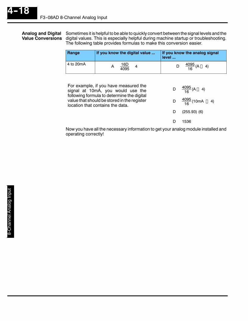
F3--0
8AD
8-C
hann
elA
nalo
gIn
put
4--18F3--08AD 8-Channel Analog Input
Sometimes it is helpful to be able to quickly convert between the signal levels and thedigital values. This is especially helpful during machine startup or troubleshooting.The following table provides formulas to make this conversion easier.
Range If you know the digital value ... If you know the analog signallevel ...
4 to 20mA
For example, if you have measured thesignal at 10mA, you would use thefollowing formula to determine the digitalvalue that should be stored in the registerlocation that contains the data.
D = 409516
(A ≡ 4)
D = 409516
(10mA ≡ 4)
D = (255.93) (6)
D = 1536
Now you have all the necessary information to get your analog module installed andoperating correctly!
Analog and DigitalValue Conversions
A = 16D4095 + 4 D = 4095
16(A ≡ 4)

15F3--16AD16-ChannelAnalog Input
In This Chapter. . . .— Module Specifications— Setting the Module Jumpers— Connecting the Field Wiring— Module Operation— Writing the Control Program

F3--1
6AD
16-C
hann
elA
nalo
gIn
put
5--2F3--16AD 16-Channel Analog Input
Module Specifications
The following table provides the specifications for the F3--16AD Analog InputModule from FACTS Engineering. Review these specifications to make sure themodule meets your application requirements.
Number of Channels 16, single ended (one common)
Input Ranges ? 5V, ? 10V, 0--5V1, 0--10V,0--20 mA, 4 -- 20 mA2
Resolution 12 bit (1 in 4096)
Input Impedance 2MO , voltage input500O ? 1%, current input
Absolute Maximum Ratings ? 25V, voltage input? 30 mA, current input
Conversion Time 35µs per channel1 channel per CPU scan
Converter Type Successive Approximation, AD574
Linearity Error ? 1 count maximum
Maximum Inaccuracy at 77 °F(25 °C)
0.25% of full scale, voltage input1.25% of full scale, current input
Accuracy vs. Temperature 57 ppm / _C maximum full scale
Recommended Fuse 0.032 A, Series 217 fast-acting, current inputs
Power Budget Requirement 33 mA @ 9 VDC, 47 mA @ 24 VDC
External Power Supply None required
Operating Temperature 32° to 140° F (0° to 60_ C)
Storage Temperature --4° to 158° F (--20° to 70_ C)
Relative Humidity 5 to 95% (non-condensing)
Environmental air No corrosive gases permitted
Vibration MIL STD 810C 514.2
Shock MIL STD 810C 516.2
Noise Immunity NEMA ICS3--3041 -- requires gain adjustment with potentiometer.
2 -- resolution is 3275 counts (instead of 4096). Allows easier broken transmitter detection
The F3--16AD Analog Input appears as a 16-point module. The module can beinstalled in any slot configured for 16 points. See the DL305 User Manual for detailson using 16 point modules in DL305 systems. The limitation on the number of analogmodules are:
S For local and expansion systems, the available power budget and16-point module usage are the limiting factors.
Analog InputConfigurationRequirements

F3--16AD
16-ChannelA
nalogInput
5--3F3--16AD 16-Channel Analog Input
Setting the Module Jumpers
The module is set at the factory for a 0--20 mA signal on all sixteen channels. If this isacceptable you do not have to change any of the jumpers. The following diagramshows the jumper locations.
Current
Channels
Span GainX100
X1000GainX1X10
ADJ
10V
20V
8421
Bipolar
UnipolarPolarity
If you examine the rear of the module,you’ll notice several jumpers. Thejumpers labeled +1, +2, +4 and +8 areused to select the number of channelsthat will be used. Without any jumpersthe module processes one channel. Byinstalling the jumpers you can addchannels. The module is set from thefactory for sixteen channel operation.Any unused channels are not processedso if you only select channels 1--8, thenthe last eight channels will not be active.The following table shows which jumpersto install.
Jumpers installed as shownselects 16-channel operation
+8 +4 +2
Number ofChannels
+1
Channel(s)Jumper
Channel(s)Jumper
Channel(s)+8 +4 +2 +1
Channel(s)+8 +4 +2 +1
1 No No No No 1 2 3 4 5 6 7 8 9 Yes No No No
1 2 No No No Yes 1 2 3 4 5 6 7 8 9 10 Yes No No Yes
1 2 3 No No Yes No 1 2 3 4 5 6 7 8 9 10 11 Yes No Yes No
1 2 3 4 No No Yes Yes 1 2 3 4 5 6 7 8 9 10 11 12 Yes No Yes Yes
1 2 3 4 5 No Yes No No 1 2 3 4 5 6 7 8 9 10 11 12 13 Yes Yes No No
1 2 3 4 5 6 No Yes No Yes 1 2 3 4 5 6 7 8 9 10 11 12 13 14 Yes Yes No Yes
1 2 3 4 5 6 7 No Yes Yes No 1 2 3 4 5 6 7 8 9 10 11 12 13 14 15 Yes Yes Yes No
1 2 3 4 5 6 7 8 No Yes Yes Yes 1 2 3 4 5 6 7 8 9 10 11 12 13141516 Yes Yes Yes Yes
Jumper Locations
Selecting theNumber ofChannels

F3--1
6AD
16-C
hann
elA
nalo
gIn
put
5--4F3--16AD 16-Channel Analog Input
As you examined the jumper settings, you may have noticed there are currentjumpers for each individual channel. These jumpers allow you to select the type ofsignal (voltage or current).The span and polarity jumpers are used to select the signal range. The polarity andspan selection affect all the channels. For example, if you select unipolar operationand a 10V span, you can use both 0 --10V and 0--20 mA signals at the same time.Channels that will receive 0--20 mA signals should have the current jumper installed.The following table shows the jumper selections for the various ranges. (Onlychannel 1 is used in the example, but all channels must be set.)
Bipolar Signal Range Jumper Settings
--5 VDC to +5 VDC
--10 VDC to +10 VDC
Unipolar Signal Range Jumper Settings
0 to 20 mA(these settings are also usedfor the 4--20mA range)
0 VDC to +10 VDC
Selecting InputSignal Ranges
PolarityUniBi
Current JumperSpan10V20V
PolarityUniBi
Current JumperSpan10V20V
PolarityUniBi
Current JumperSpan10V20V
PolarityUniBi
Current JumperSpan10V20V
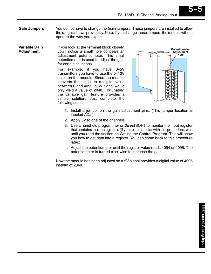
F3--16AD
16-ChannelA
nalogInput
5--5F3--16AD 16-Channel Analog Input
You do not have to change the Gain jumpers. These jumpers are installed to allowthe ranges shown previously. Note, if you change these jumpers the module will notoperate the way you expect.
If you look at the terminal block closely,you’ll notice a small hole conceals anadjustment potentiometer. This smallpotentiometer is used to adjust the gainfor certain situations.For example, if you have 0--5Vtransmitters you have to use the 0--10Vscale on the module. Since the moduleconverts the signal to a digital valuebetween 0 and 4095, a 5V signal wouldonly yield a value of 2048. Fortunately,the variable gain feature provides asimple solution. Just complete thefollowing steps.
PotentiometerAdjustment
Hole
1. Install a jumper on the gain adjustment pins. (This jumper location islabeled ADJ.)
2. Apply 5V to one of the channels.3. Use a handheld programmer or DirectSOFT to monitor the input register
that contains the analog data. (If you’re not familiar with this procedure, waituntil you read the section on Writing the Control Program. This will showyou how to get data into a register. You can come back to this procedurelater.)
4. Adjust the potentiometer until the register value reads 4094 or 4095. Thepotentiometer is turned clockwise to increase the gain.
Now the module has been adjusted so a 5V signal provides a digital value of 4095instead of 2048.
Gain Jumpers
Variable GainAdjustment

F3--1
6AD
16-C
hann
elA
nalo
gIn
put
5--6F3--16AD 16-Channel Analog Input
Connecting the Field Wiring
Your company may have guidelines for wiring and cable installation. If so, you shouldcheck those before you begin the installation. Here are some general things toconsider.
S Use the shortest wiring route whenever possible.S Use shielded wiring and ground the shield at the signal source. Do not
ground the shield at both the module and the source.S Don’t run the signal wiring next to large motors, high current switches, or
transformers. This may cause noise problems.S Route the wiring through an approved cable housing to minimize the risk
of accidental damage. Check local and national codes to choose thecorrect method for your application.
The F3--16AD receives all power from the base. A separate power supply is notrequired.
Wiring Guidelines
User Power SupplyRequirements

F3--16AD
16-ChannelA
nalogInput
5--7F3--16AD 16-Channel Analog Input
Occasionally you may have the need to connect a transmitter with an unusual signalrange. By changing the wiring slightly and adding an external resistor to convert thecurrent to voltage, you can easily adapt this module to meet the specifications for atransmitter that does not adhere to one of the standard input ranges. The followingdiagram shows how this works.
R =Vmax
Imax
R = value of external resistorVmax = high limit of selected voltage rangeImax = maximum current supplied by the transmitter
Example: current transmitter capable of 50mA, 0 -- 10V range selected.
R =10V
50mAR = 200 ohms
Internal
+CH1
COM
+
--250O
R
JumperRemoved
ModuleCircuitry
50mACurrent
Transmitter
NOTE: Your choice of resistor can affect the accuracy of the module. A resistor thathas ? 0.1% tolerance and a ? 50ppm / _C temperature coefficient is recommended.
Custom InputRanges

F3--1
6AD
16-C
hann
elA
nalo
gIn
put
5--8F3--16AD 16-Channel Analog Input
Standard 4 to 20 mA transmitters and transducers can operate from a wide variety ofpower supplies. Not all transmitters are alike and the manufacturers often specify aminimum loop or load resistance that must be used with the transmitter at the variousvoltages.The F3--16AD provides 500 ohm resistance for each channel. If your transmitterrequires a load resistance below 500 ohms, then you do not have to make anyadjustments. However, if your transmitter requires a load resistance higher than 500ohms, then you need to add a resistor in series with the module.Consider the following example for a transmitter being operated from a 36 VDCsupply with a recommended load resistance of 750 ohms. Since the module has a500 ohm resistor, you need to add an additional resistor.
0V+36V
DC Supply
Two-wire Transmitter
+ --
R = Tr ≡ Mr R -- Resistor to addTr -- Transmitter RequirementMr -- Module resistance (internal 500 ohms)
R = 750 ≡ 500
R = 250
--+
Module Channel 1
R 500O
Current LoopTransmitterImpedance

F3--16AD
16-ChannelA
nalogInput
5--9F3--16AD 16-Channel Analog Input
The F3--16AD module has a removable connector to make wiring easier. Simplysqueeze the top and bottom tabs and gently pull the connector from the module.
ANALOG INPUTF3--16AD
COM
CH
4
CH
2
CH
6CH
8
COM
CH
12
CH
10
CH
14CH
16
CH
3
CH
1
CH
5CH
7
CH
11
CH
9
CH
13CH
15
+
+
+
+
+
+
+
+
+
+
+
+
+
+
+
+
CH1Volatage
Transmitter
CurrentTransmitter
CurrentTransmitter
CurrentTransmitter
CurrentTransmitter
CH2
CH3
CH4
CH5
CH6
CH7
CH8
CH9
CH10
CH11
CH12
CH13
CH14
CH15
CH16
VolatageTransmitter
VolatageTransmitter
VolatageTransmitter
VolatageTransmitter
VolatageTransmitter
VolatageTransmitter
VolatageTransmitter
VolatageTransmitter
VolatageTransmitter
VolatageTransmitter
VolatageTransmitter
AnalogSwitch
All resistors are 500O
See note
Note 1: Terminate all shields at their respective signal source.Note 2: Jumpers for CH4, 7, 12 and 16 are installed for current input.
Internal Module Wiring
1
3
5
7
9
11
13
15
COM
COM
2
4
6
8
10
12
14
16
RemovableConnector
Wiring Diagram

F3--1
6AD
16-C
hann
elA
nalo
gIn
put
5--10F3--16AD 16-Channel Analog Input
Module Operation
Before you begin writing the control program, it is important to take a few minutes tounderstand how the module processes and represents the analog signals.The F3--16AD module supplies 1 channel of data per each CPU scan. Since thereare sixteen channels, it can take up to sixteen scans to get data for all channels.Once all channels have been scanned the process starts over with channel 1.You do not have to select all of the channels. Unused channels are not processed, soif you select only eight channels, then the channels will be updated within eightscans.
I/O Update
Channel 1 Scan N
Read the data
Store data
Execute Application ProgramChannel 2 Scan N+1
Channel 16 Scan N+15
Channel 1 Scan N+16
Scan
.
.
.
.
.
.
Even though the channel updates to the CPU are synchronous with the CPU scan,the module asynchronously monitors the analog transmitter signal and converts thesignal to a 12-bit binary representation. This enables the module to continuouslyprovide accurate measurements without slowing down the discrete control logic inthe RLL program.
Channel ScanningSequence
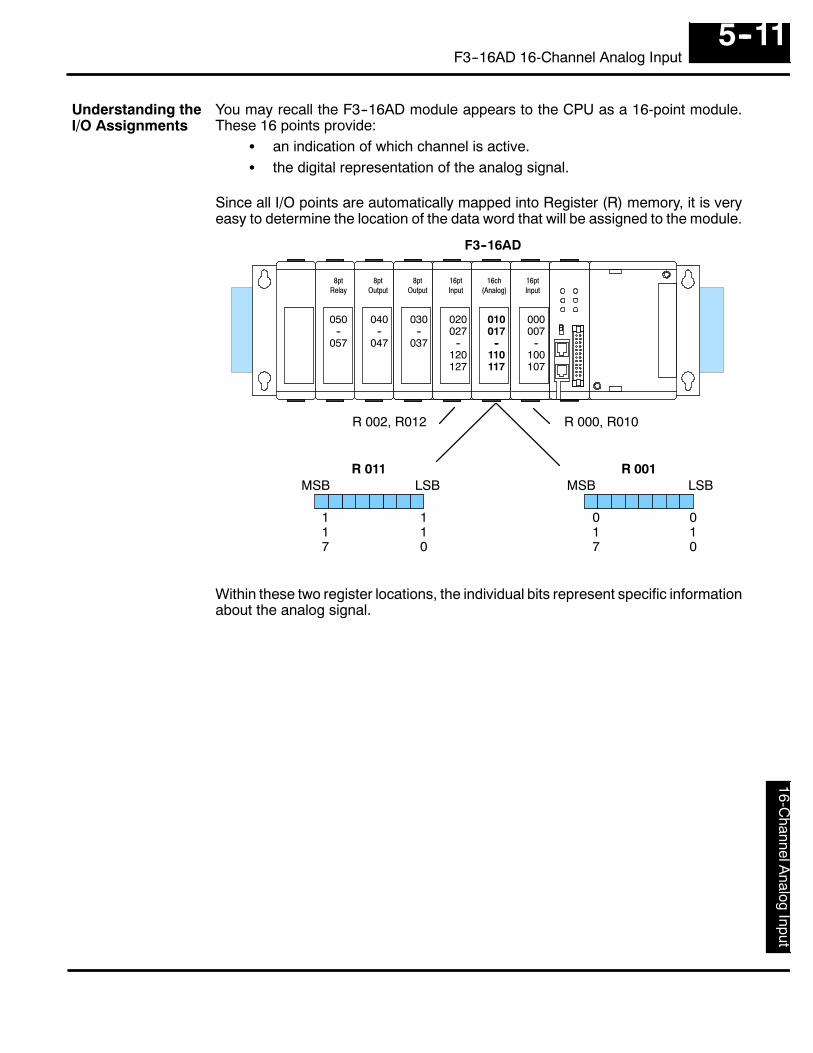
F3--16AD
16-ChannelA
nalogInput
5--11F3--16AD 16-Channel Analog Input
You may recall the F3--16AD module appears to the CPU as a 16-point module.These 16 points provide:
S an indication of which channel is active.S the digital representation of the analog signal.
Since all I/O points are automatically mapped into Register (R) memory, it is veryeasy to determine the location of the data word that will be assigned to the module.
110
F3--16AD
R 011MSB LSB
R 001MSB LSB
010
R 002, R012 R 000, R010
117
8ptRelay
8ptOutput
16ptInput
16pt(Analog)
16chInput
8ptOutput
050--
057
040--
047
030--
037
020027
--120127
000007
--100107
010017
--110117
017
Within these two register locations, the individual bits represent specific informationabout the analog signal.
Understanding theI/O Assignments

F3--1
6AD
16-C
hann
elA
nalo
gIn
put
5--12F3--16AD 16-Channel Analog Input
The last four inputs of the upper Registerindicate the active channel. Theindicators automatically increment witheach CPU scan.
Channel ActiveScan Inputs ChannelN 0000 1N+1 0001 2N+2 0010 3N+3 0011 4N+4 0100 5N+5 0101 6N+6 0110 7N+7 0111 8N+8 1000 9N+9 1001 10N+10 1010 11N+11 1011 12N+12 1100 13N+13 1101 14N+14 1110 15N+15 1111 16
R011MSB LSB
110
117
116
115
114
113
112
111
-- channel indicator inputs
Active ChannelIndicator Inputs

F3--16AD
16-ChannelA
nalogInput
5--13F3--16AD 16-Channel Analog Input
The remaining twelve bits represent theanalog data in binary format.Bit Value Bit Value0 (LSB) 1 6 641 2 7 1282 4 8 2563 8 9 5124 16 10 10245 32 11 2048
117
R001MSB LSB
010
116
115
114
113
112
111
110
017
016
015
014
013
012
011
-- data bits
R011
Since the module has 12-bit resolution, the analog signal is converted into 4096“pieces” ranging from 0 -- 4095 (212). For example, with a 0 to 10V scale, a 0V signalwould be 0, and a 10V signal would be 4095. This is equivalent to a a binary value of0000 0000 0000 to 1111 1111 1111, or 000 to FFF hexadecimal. The followingdiagram shows how this relates to each signal range.
+V
0V
--V0 4095
--10V -- +10V--5V -- +5V
+V
0V0 4095
0V -- 10V
20mA
0mA0 4095
0 -- 20mA
20mA
4mA
819 4095
4 -- 20mA
0
NOTE: When you use 4--20mA signals, you have to use the 0--20mA scale. You donot have resolution of 4096 if the 4--20mA signal is present. In this case, the range is819 to 4095. This is because a 0 still represents 0mA, not 4mA.
Each “piece” can also be expressed interms of the signal level by using theequation shown. The following tableshows the smallest signal levels that willpossibly result in a change in the datavalue for each signal range.
Resolution = H ≡ L4095
H = high limit of the signal rangeL = low limit of the signal range
Range Highest Signal Lowest Signal Smallest Change
--10 to +10V +10V --10V 4.88 mV
--5 to +5V +5 V --5V 2.44 mV
0 to 10V 10V 0V 2.44 mV
0 to 20mA(4 to 20mA also)
20mA 0mA 4.88 µA
Now that you understand how the module and CPU work together to gather andstore the information, you’re ready to write the control program.
Analog Data Bits
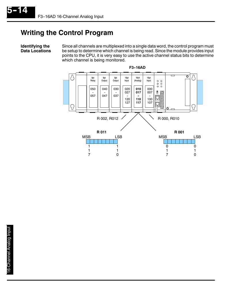
F3--1
6AD
16-C
hann
elA
nalo
gIn
put
5--14F3--16AD 16-Channel Analog Input
Writing the Control Program
Since all channels are multiplexed into a single data word, the control program mustbe setup to determine which channel is being read. Since the module provides inputpoints to the CPU, it is very easy to use the active channel status bits to determinewhich channel is being monitored.
110
F3--16AD
R 011MSB LSB
R 001MSB LSB
010
R 002, R012 R 000, R010
117
8ptRelay
8ptOutput
16ptInput
16pt(Analog)
16chInput
8ptOutput
050--
057
040--
047
030--
037
020027
--120127
000007
--100107
010017
--110117
017
Identifying theData Locations

F3--16AD
16-ChannelA
nalogInput
5--15F3--16AD 16-Channel Analog Input
The following example shows a program designed to read any of the availablechannels of analog data into Register locations. Once the data is in a Register, youcan perform math on the data, compare the data against preset values, etc. Sincethe DL305 CPUs use 8-bit word instructions, you have to move the data in pieces. It’spretty simple if you follow the example.
374DSTR3R011
F53
Read the data
This rung loads the four most significant data bits intothe accumulator from Register 011 on every scan.
DOUT1R501
F61
114DOUTR400
F60
Store channel 1
DOUTR402
F60
Store channel 2
This rung shows how you would use the channelindicator inputs as contacts to control the channelselection.
This rung shows an easier way. Earlier we loadedthe channel ID bits (in BCD format) into R600. Nowwe can use one relational contact to examine thisvalue. However, this method uses the registerassociated with Timer/Counter 600. If you use thismethod, make sure you don’t use theTimer/Counter associated with the registerelsewhere in the program.
Temporarily store the bits to Register 501.
DSTR1R001
F51 This rung loads the eight least significant data bitsinto the accumulator from Register 001.
DOUT1R500
F61 Temporarily store the bits to Register 500. Sincethe most significant bits were loaded into 501, nowR500 and R501 contain all twelve bits in order.
DSTRR500
F50
BCD F86
Now that all the bits are stored, load all twelve bitsinto the accumulator.
Math operations are performed in BCD. Thisinstruction converts the binary data to BCD. (Youcan omit this step if your application does notrequire the conversion.)
115 117
CT600
DOUTR434
F60
Store channel 15
DOUTR436
F60
Store channel 16
374DSTR2R011
F52 This rung loads the channel ID bits into theaccumulator from Register 011 on every scan.
BCD F86 Convert the channel ID status to BCD. (We’ll userelational contacts later to make the chanelselection much easier.)
DOUTR600
F60 Store the channel ID in R600. (Note, you don’tabsolutely have to do it this way. If you use R600,then you can’t use Timer/Counter 600. You couldjust use the channel indicators. See the StoreChannel 1 example that follows.)
Read the channel ID
The channel selection inputs are used to let theCPU know which channel has been loaded into theaccumulator. By using these inputs to control aDOUT instruction, you can easily move the data toa storage register. Notice the DOUT instructionstores the data in two bytes. (Two bytes arerequired for four digit BCD numbers.)
116
=K0001
CT600
=K0014
CT600
=K0015
Example Program

F3--1
6AD
16-C
hann
elA
nalo
gIn
put
5--16F3--16AD 16-Channel Analog Input
The example below shows how to read multiple channels on an F3--08AD Analogmodule in the 20--27/120--127 address slot. This module must be placed in a 16 bitslot in order to work.
This sends channel one analog data toV3000 when bits X124, X125, X126and X127 are as shown.
LD
_On
LDF
K8
X120This rung loads the upper byte of analog data fromthe module.
Load the data
SP1
BCD
V2200
Channel 1 Select Bit States
SHFL
ANDD
ORF
K8
X20
K8
Kfff
The ORF X20 brings the lower byte of data fromthe module into the accumulator. At this time thereis a full word of data from the analog module in theaccumulator.
SHFL K8 shifts the data to the left eight places tomake room for the lower byte of data.
The ANDD Kfff masks off the twelve leastsignificant bits of data from the word. This is theactual analog value.
The BCD command converts the data to BCDformat.
X125X124 X126 X127
OUTV2200
Stores the data in V2200.
OUTV3000
This sends channel two analog data toV3000 when bits X124, X125, X126and X127 are as shown.
LD
V2200
Channel 2 Select Bit States
X125X124 X126 X127
OUTV3001
This sends channel two analog data toV3000 when bits X124, X125, X126and X127 are as shown.
LD
V2200
Channel 3 Select Bit States
X125X124 X126 X127
OUTV3002
DL350 with aConventionalDL305 Base

F3--16AD
16-ChannelA
nalogInput
5--17F3--16AD 16-Channel Analog Input
The example below shows how to read multiple channels on an F3--16AD Analogmodule in the X0 address of the D3--XX--1 base.
_On
LD VX0 This rung loads the upper byte of analog data fromthe module.
SP1
SHFRK12
SHFL K12 shifts the word to the right twelveplaces.
OUTV1400 Puts the four channel select bits in the lower nibble
(four bits) of word V1400. This will increment oncewith each scan from 0 to F.
_On
LDF X0 This rung loads the twelve bits of analog data tothe module and converts it to BCD. It is the OUT toV1401.
SP1
BCD
OUTV1401 The analog data (in BCD format) is then stored in
the Holding Register, V1401.
Channel Selection Data
LDV1401
Rungs 3--18 compare the count of the chennel select bits. When the corresponding bits are true, thechannel data for that channel is stored in the proper V-memory location. For sixteen channels ofanalog data, the module will require sixteen scans in order to update all channels.
V1400
OUTV2000
=K0
K12
This convertsthe data to BCD.
Channel #1 Data
Channel Selection Data
LDV1401
V1400
OUTV2001
=K1
Channel #2 Data
Channel Selection Data
LDV1401
V1400
OUTV2002
=K2
Channel #3 Data
DL350 with aD3--XX--1 Base
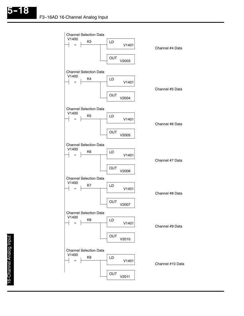
F3--1
6AD
16-C
hann
elA
nalo
gIn
put
5--18F3--16AD 16-Channel Analog Input
Channel Selection Data
LDV1401
V1400
OUTV2004
=K4
Channel Selection Data
LDV1401
V1400
OUTV2003
=K3
Channel Selection Data
LDV1401
V1400
OUTV2005
=K5
Channel Selection Data
LDV1401
V1400
OUTV2006
=K6
Channel #4 Data
Channel #5 Data
Channel #6 Data
Channel #7 Data
Channel Selection Data
LDV1401
V1400
OUTV2007
=K7
Channel Selection Data
LDV1401
V1400
OUTV2010
=K8
Channel Selection Data
LDV1401
V1400
OUTV2011
=K9
Channel #8 Data
Channel #9 Data
Channel #10 Data

F3--16AD
16-ChannelA
nalogInput
5--19F3--16AD 16-Channel Analog Input
Channel Selection Data
LDV1401
V1400
OUTV2012
=Ka
Channel Selection Data
LDV1401
V1400
OUTV2013
=Kb
Channel Selection Data
LDV1401
V1400
OUTV2014
=Kc
Channel #11 Data
Channel #12 Data
Channel #13 Data
Channel Selection Data
LDV1401
V1400
OUTV2015
=Kd
Channel Selection Data
LDV1401
V1400
OUTV2016
=Ke
Channel Selection Data
LDV1401
V1400
OUTV2017
=Kf
Channel #14 Data
Channel #15 Data
Channel #16 Data

F3--1
6AD
16-C
hann
elA
nalo
gIn
put
5--20F3--16AD 16-Channel Analog Input
Most applications usually requiremeasurements in engineering units,which provide more meaningful data.This is accomplished by using theconversion formula shown.
Units = A4096 S
Units = value in Engineering UnitsA = Analog value (0 -- 4095)S = high limit of the Engineeringunit range
The following example shows how youwould use the analog data to representpressure (PSI) from 0 to 100. Thisexample assumes the analog value is1760. This should yield approximately42.9 PSI.
Units = 17604096
100
Units = A4096 S
Units = 42.9
Scaling the InputData
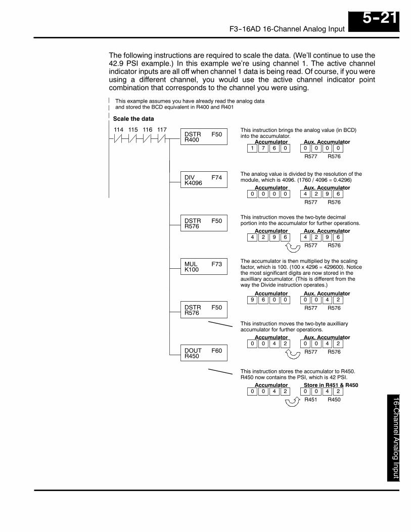
F3--16AD
16-ChannelA
nalogInput
5--21F3--16AD 16-Channel Analog Input
The following instructions are required to scale the data. (We’ll continue to use the42.9 PSI example.) In this example we’re using channel 1. The active channelindicator inputs are all off when channel 1 data is being read. Of course, if you wereusing a different channel, you would use the active channel indicator pointcombination that corresponds to the channel you were using.
DSTRR400
F50
DIVK4096
F74
This instruction brings the analog value (in BCD)into the accumulator.
This instruction moves the two-byte decimalportion into the accumulator for further operations.
Scale the data
The analog value is divided by the resolution of themodule, which is 4096. (1760 / 4096 = 0.4296)
DSTRR576
F50
MULK100
F73
DSTRR576
F50
DOUTR450
F60
1 7 6 0Accumulator
0 0 0 0Aux. Accumulator
0 0 0 0Accumulator
4 2 9 6Aux. Accumulator
This example assumes you have already read the analog dataand stored the BCD equivalent in R400 and R401
4 2 9 6Accumulator
4 2 9 6Aux. Accumulator
The accumulator is then multiplied by the scalingfactor, which is 100. (100 x 4296 = 429600). Noticethe most significant digits are now stored in theauxilliary accumulator. (This is different from theway the Divide instruction operates.)
9 6 0 0Accumulator
0 0 4 2Aux. Accumulator
R577 R576
R577 R576
R577 R576
R577 R576
This instruction moves the two-byte auxilliaryaccumulator for further operations.
0 0 4 2Accumulator
0 0 4 2Aux. Accumulator
R577 R576
This instruction stores the accumulator to R450.R450 now contains the PSI, which is 42 PSI.
0 0 4 2Accumulator
0 0 4 2Store in R451 & R450
R451 R450
114 115 117116
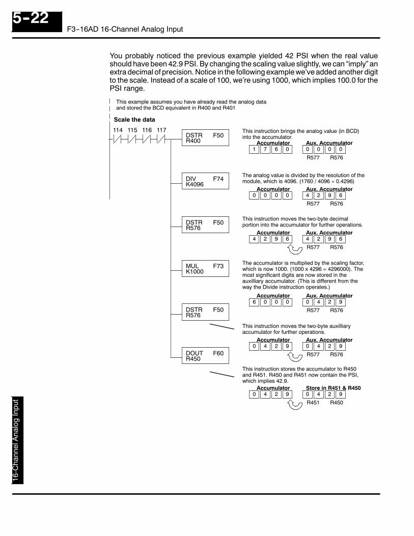
F3--1
6AD
16-C
hann
elA
nalo
gIn
put
5--22F3--16AD 16-Channel Analog Input
You probably noticed the previous example yielded 42 PSI when the real valueshould have been 42.9 PSI. By changing the scaling value slightly, we can “imply” anextra decimal of precision. Notice in the following example we’ve added another digitto the scale. Instead of a scale of 100, we’re using 1000, which implies 100.0 for thePSI range.
DSTRR400
F50
DIVK4096
F74
This instruction brings the analog value (in BCD)into the accumulator.
This instruction moves the two-byte decimalportion into the accumulator for further operations.
Scale the data
The analog value is divided by the resolution of themodule, which is 4096. (1760 / 4096 = 0.4296)
DSTRR576
F50
MULK1000
F73
DSTRR576
F50
DOUTR450
F60
1 7 6 0Accumulator
0 0 0 0Aux. Accumulator
0 0 0 0Accumulator
4 2 9 6Aux. Accumulator
This example assumes you have already read the analog dataand stored the BCD equivalent in R400 and R401
4 2 9 6Accumulator
4 2 9 6Aux. Accumulator
The accumulator is multiplied by the scaling factor,which is now 1000. (1000 x 4296 = 4296000). Themost significant digits are now stored in theauxilliary accumulator. (This is different from theway the Divide instruction operates.)
6 0 0 0Accumulator
0 4 2 9Aux. Accumulator
R577 R576
R577 R576
R577 R576
R577 R576
This instruction moves the two-byte auxilliaryaccumulator for further operations.
0 4 2 9Accumulator
0 4 2 9Aux. Accumulator
R577 R576
This instruction stores the accumulator to R450and R451. R450 and R451 now contain the PSI,which implies 42.9.
0 4 2 9Accumulator
0 4 2 9Store in R451 & R450
R451 R450
114 115 117116

F3--16AD
16-ChannelA
nalogInput
5--23F3--16AD 16-Channel Analog Input
This example program shows how you can use the instructions to load theseequation constants into data registers. The example is written for channel 1, but youcan easily use a similar approach to use different scales for all channels if required.You may just use the appropriate constants in the instructions dedicated for eachchannel, but this method allows easier modifications. For example, you could easilyuse an operator interface or a programming device to change the constants if theyare stored in Registers.
This rung loads the four most significant data bits intothe accumulator from Register 011 on every scan.
Temporarily store the bits to Register 501.
DSTR3R011
F53
DOUT1R501
F61
374Read the data
Store channel 1
374DSTRK4096
F50
DOUTR460
F60
DSTRK1000
F50
DOUTR462
F60
On the first scan, these first two instructions loadthe analog resolution (constant of 4096) into R460and R461.
These two instructions load the high limit of theEngineering unit scale (constant of 1000) intoR462 and R463. Note, if you have different scalesfor each channel, you’ll also have to enter theEngineering unit high limit for those as well.
Load the constants
DIVR460
F74
DSTRR576
F50
MULR462
F73
This instruction moves the decimal portion from theauxilliary accumulator into the regular accumulatorfor further operations.
The analog value is divided by the resolution of themodule, which is stored in R460.
DSTRR576
F50
DOUTR400
F60
The accumulator is multiplied by the scaling factor,which is stored in R462.
This instruction moves most significant digits (nowstored in the auxilliary accumulator) into theregular accumulator for further operations.
The scaled value is stored in R400 and R401 forfurther use.
114 115 117116

F3--1
6AD
16-C
hann
elA
nalo
gIn
put
5--24F3--16AD 16-Channel Analog Input
The example below shows how to scale input data from an F3--04ADS Analogmodule in the 20--27/120--127 address slot. This module must be placed in a 16 bitslot in order to work.
_On
LDF
K8
X120
SHFL K8
ORF
K8
X20
ANDD Kfff
This loads the upper byte of the analog data fromthe module.
The ORF X20 brings the lower byte of data fromthe module into the accumulator. At this time thereis a full word of data from the analog module in theaccumulator.
Load the data
MUL K2000
Rung 3 scales a 0 to 200 range of a transducerover the 4096 counts. The raw analog value isloaded to the accumulator from V3001(Channel #1).
DIV K4096
OUT V3010
It is then multiplied by 2000. The additional zeroprovides a higher degree of resolution.
It is then divided by 4096, which is the resolution ofthe module.
The scaled value is stored in V3010 with animplied decimal.
SP1
SHFL K8 shifts the data to the left eight places tomake room for the lower byte of data.
BCD
The ANDD Kfff masks off the twelve leastsignificant bits of data from the word. This is theactual analog value.
The BCD command converts the data to BCDformat.
_OnSP1 LD
Channel 2Analog DataRegister (BCD)
V3000
Scale the data
OUT V2200 The scaled value is stored in V3010 with animplied decimal.
This writes channel one analog data toV3000 when bits X124, X125, X126and X127 are as shown.
LD
V2200
Channel 1 Select Bit States
X125X124 X126 X127
OUTV3000
Scaling on a DL350with aConventionalDL305 Base

F3--16AD
16-ChannelA
nalogInput
5--25F3--16AD 16-Channel Analog Input
If you use 4--20mA signals you can easily check for broken transmitter conditions.Since you have to use the 0--20mA range and the lowest signal for the 4--20mAtransmitter is 4mA, the lowest digital value for the signal is not 0, but instead is 819.If the transmitter is working properly the smallest value you should ever see is 819. Ifyou see a value of less than about 750 (allowing for tolerance), then you know thetransmitter is broken.
374DSTR3R011
F53
Read the data
This rung loads the four most significant data bits intothe accumulator from Register 011 on every scan.
DOUT1R501
F61
DOUTR400
F60
Store channel 1
Temporarily store the bits to Register 501.
DSTR1R001
F51 This rung loads the eight least significant data bitsinto the accumulator from Register 001.
DOUT1R500
F61 Temporarily store the bits to Register 500. Sincethe most significant bits were loaded into 501, nowR500 and R501 contain all twelve bits in order.
DSTRR500
F50
BCD F86
Now that all the bits are stored, load all twelve bitsinto the accumulator.
Math operations are performed in BCD. Thisinstruction converts the binary data to BCD. (Youcan omit this step if your application does notrequire the conversion.)
DSTR2R011
F52 This rung loads the channel ID bits into theaccumulator from Register 011 on every scan.
BCD F86 Convert the channel ID status to BCD. We’ll userelational contacts later to make the chanelselection much easier.)
DOUTR600
F60 Store the channel ID in R600.
Read the channel ID
The DOUT instruction copies the accumulator datato R400 and R401. Since the data is still in theaccumulator, we can compare it against aconstant. Since the minimum value for a 4mAsignal is 819 (minus the module tolerance), we canchoose a value for the compare. We picked 100,but you could choose something else from 0 toabout 750.
Flags 773 and 774 are used with the Compareinstruction. In this example if the analog value isless than or equal to 100, then output 040 is turnedon.
You may want to latch 040 to catch intermittentbroken transmitters.
CMPK0100
F70
773OUT040
Broken transmitter indicator on channel 1
774
114 115 117116
114 115 117116
374
Broken TransmitterDetection

F3--1
6AD
16-C
hann
elA
nalo
gIn
put
5--26F3--16AD 16-Channel Analog Input
Sometimes it is helpful to be able to quickly convert between the signal levels and thedigital values. This is especially helpful during machine startup or troubleshooting.The following table provides formulas to make this conversion easier.
Range If you know the digital value ... If you know the analog signallevel ...
--10V to + 10V
--5V to + 5V
0 to 10V
0 to 20mA(or 4--20mA)
For example, if you are using the --10 to+10V range and you have measured thesignal at 6V, you would use the followingformula to determine the digital valuethat should be stored in the registerlocation that contains the data.
D = 409520
(A + 10)
D = 409520
(6V + 10)
D = (204.75) (16)
D = 3276
Now you have all the necessary information to get your analog module installed andoperating correctly!
Analog and DigitalValue Conversions
A = 20D4095 ≡ 10 D = 4095
20(A + 10)
A = 10D4095 ≡ 5 D = 4095
10(A + 5)
A = 10D4095 D = 4095
10A
A = 20D4095 D = 4095
20A

16D3--02DA2--ChannelAnalog Output
In This Chapter. . . .— Module Specifications— Connecting the Field Wiring— Module Operation— Writing the Control Program

D3-
-02D
A2-
Cha
nnel
Ana
log
Out
put
6--2D3--02DA 2-Channel Analog Output
Module Specifications
The following table provides the specifications for the D3--02DA Analog OutputModule. Review these specifications to make sure the module meets yourapplication requirements.
Number of Channels 2 (independent)
Output Ranges 0 -- 10V, 4 -- 20 mA
Resolution 8 bit (1 in 256)
Output Type Single ended
Output Impedance .5O maximum, voltage output
Output Current 10 mA minimum, voltage output @ 10 VDC
Load Impedance 550O maximum, 5O minimum, current output
Total Inaccuracy ? 0.4% maximum at 25_ C
Accuracy vs. Temperature ? 50 ppm / _C maximum
Conversion Time 100µs maximum (2 channels/scan)
Power Budget Requirement 80 mA @9V
External Power Supply 24 VDC, ? 10%, 170 mA, class 2
Operating Temperature 32° to 140° F (0° to 60_ C)
Storage Temperature --4° to 158° F (--20° to 70_ C)
Relative Humidity 5 to 95% (non-condensing)
Environmental air No corrosive gases permitted
Vibration MIL STD 810C 514.2
Shock MIL STD 810C 516.2
Noise Immunity NEMA ICS3--304
The D3--02DA Analog Output appears as a 16-point module. The module can beinstalled in any slot configured for 16 points. See the DL305 User Manual for detailson using 16 point modules in DL305 systems. The limitation on the number of analogmodules are:
S For local and expansion systems, the available power budget and16-point module usage are the limiting factors.
Analog OutputConfigurationRequirements

D3--02D
A2-C
hannelAnalog
Output
6--3D3--02DA 2-Channel Analog Output
Connecting the Field Wiring
Your company may have guidelines for wiring and cable installation. If so, you shouldcheck those before you begin the installation. Here are some general things toconsider.
S Use the shortest wiring route whenever possible.S Use shielded wiring and ground the shield at the module or the power
supply return (0V). Do not ground the shield at both the module and thetransducer.
S Don’t run the signal wiring next to large motors, high current switches, ortransformers. This may cause noise problems.
S Route the wiring through an approved cable housing to minimize the riskof accidental damage. Check local and national codes to choose thecorrect method for your application.
The D3--02DA requires a separate power supply. Choose a supply that meets thefollowing requirements: 24 VDC ? 10%, Class 2, 170mA current (or greater,depending on the number of modules being used.)
Each channel can be wired independently for a voltage or current transducer.S Current transducers must have an impedance between 5 and 550 ohmsS Voltage transducers must have an impedance greater than 1K ohms.
Wiring Guidelines
User Power SupplyRequirements
LoadRequirements
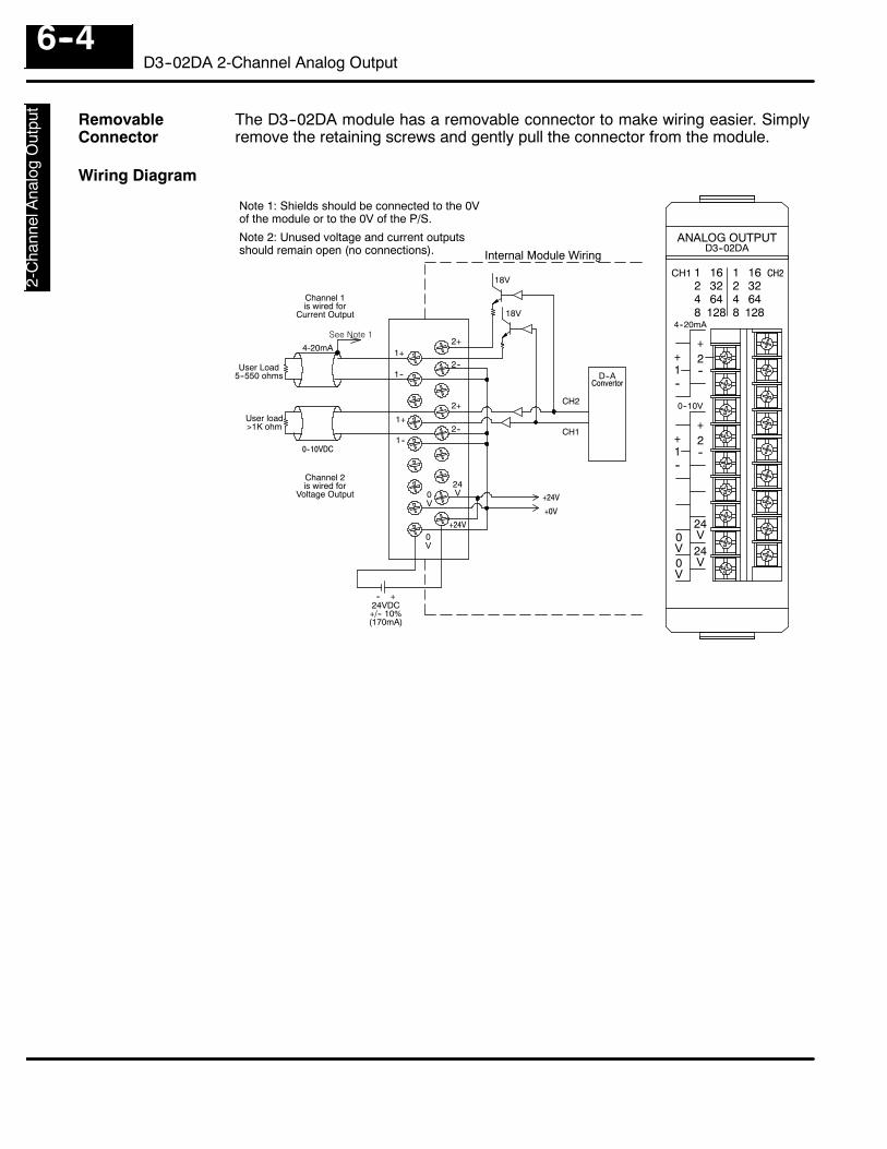
D3-
-02D
A2-
Cha
nnel
Ana
log
Out
put
6--4D3--02DA 2-Channel Analog Output
The D3--02DA module has a removable connector to make wiring easier. Simplyremove the retaining screws and gently pull the connector from the module.
1248
ANALOG OUTPUTD3--02DA
+
--
0
--
24
+
24
163264
128
0
0
24
+24V
CH1 CH2
2
V
V
1
V
V
V
V
V
24VDC-- +
Note 1: Shields should be connected to the 0Vof the module or to the 0V of the P/S.
Note 2: Unused voltage and current outputsshould remain open (no connections).
D--AConvertor
18V
CH1
1248
163264
128
0
+
----
+2
1
0--10V
4--20mA
4-20mA
User Load
0--10VDC
>1K ohm
+/-- 10%(170mA)
1+
1--
1+
1--
2+
2--
2+
2--
+24V
CH2
18V
+0V
Channel 2is wired for
Voltage Output
See Note 1
5--550 ohms
User load
Channel 1is wired for
Current Output
Internal Module Wiring
RemovableConnector
Wiring Diagram

D3--02D
A2-C
hannelAnalog
Output
6--5D3--02DA 2-Channel Analog Output
Module Operation
Before you begin writing the control program, it is important to take a few minutes tounderstand how the module processes and represents the analog signals.The D3--02DA module updates both channels in the same scan. The controlprogram updates the two channels of this module independent of each other andeach channel does not have to be refreshed on each scan.
Channel 1Scan N
Calculate the data
Write data
I/O Update
Execute Application Program
Scan N+1
Scan N+2
Scan N+3
Scan N+4
Scan
Channel 2
Channel 1
Channel 2
Channel 1
Channel 2
Channel 1
Channel 2
Channel 1
Channel 2
Channel ScanningSequence

D3-
-02D
A2-
Cha
nnel
Ana
log
Out
put
6--6D3--02DA 2-Channel Analog Output
You may recall the D3--02DA module appears to the CPU as a 16-point module.These 16 points provide the digital representation of the analog signal.Since all I/O points are automatically mapped into Register (R) memory, it is veryeasy to determine the location of the data word that will be assigned to the module.
110
D3--02DA
R 011MSB LSB
R 001MSB LSB
010
R 002, R012 R 000, R010
117
8ptRelay
8ptOutput
16ptInput
16pt(Analog)
2chInput
8ptOutput
050--
057
040--
047
030--
037
020027
--120127
000007
--100107
010017
--110117
017
Channel 1Channel 2
Within these two word locations, the individual bits represent specific informationabout the analog signal.
Understanding theI/O Assignments

D3--02D
A2-C
hannelAnalog
Output
6--7D3--02DA 2-Channel Analog Output
R001MSB LSB
010
017
-- analog data bits
The first register contains the data forchannel one (R001). The second registercontains the data for channel two (R011).Bit Value Bit Value0 1 4 161 2 5 322 4 6 643 8 7 128
Since the module has 8-bit resolution, the analog signal is converted into 256“pieces” ranging from 0 -- 255 (28). For example, with a 0 to 10V scale, a 0V signalwould be 0, and a 10V signal would be 255. This is equivalent to a a binary value of0000 0000 to 1111 1111, or 00 to FF hexadecimal. The following diagram shows howthis relates to each signal range.
+10V
0V0 255
0V -- 10V
20mA
4mA
0 255
4 -- 20mA
Each “piece” can also be expressed interms of the signal level by using theequation shown. The following tableshows the smallest signal levels that willresult in a change in the data value foreach signal range.
Resolution = H ≡ L255
H = high limit of the signal rangeL = low limit of the signal range
Range Highest Signal Lowest Signal Smallest Change
0 to 10V 10V 0V 39 mV
4 to 20mA 20mA 4mA 62.5 µA
Now that you understand how the module and CPU work together to gather andstore the information, you’re ready to write the control program.
Analog Data Bits
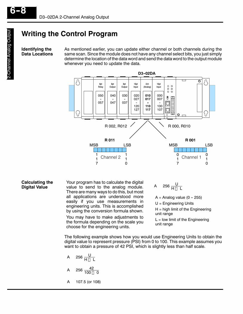
D3-
-02D
A2-
Cha
nnel
Ana
log
Out
put
6--8D3--02DA 2-Channel Analog Output
Writing the Control Program
As mentioned earlier, you can update either channel or both channels during thesame scan. Since the module does not have any channel select bits, you just simplydetermine the location of the data word and send the data word to the output modulewhenever you need to update the data.
110
D3--02DA
R 011MSB LSB
R 001MSB LSB
010
R 002, R012 R 000, R010
117
8ptRelay
8ptOutput
16ptInput
16pt(Analog)
2chInput
8ptOutput
050--
057
040--
047
030--
037
020027
--120127
000007
--100107
010017
--110117
017
Channel 1Channel 2
Your program has to calculate the digitalvalue to send to the analog module.There are many ways to do this, but mostall applications are understood moreeasily if you use measurements inengineering units. This is accomplishedby using the conversion formula shown.You may have to make adjustments tothe formula depending on the scale youchoose for the engineering units.
A = 256 UH ≡ L
A = Analog value (0 -- 255)U = Engineering UnitsH = high limit of the Engineeringunit rangeL = low limit of the Engineeringunit range
The following example shows how you would use Engineering Units to obtain thedigital value to represent pressure (PSI) from 0 to 100. This example assumes youwant to obtain a pressure of 42 PSI, which is slightly less than half scale.
A = 256 UH ≡ L
A = 107.5 (or 108)
A = 256 42100 ≡ 0
Identifying theData Locations
Calculating theDigital Value

D3--02D
A2-C
hannelAnalog
Output
6--9D3--02DA 2-Channel Analog Output
Here’s how you would write the program to perform the Engineering Unit conversion.This example assumes you have calculated or loaded the engineering unit valueand stored it in R400. Also, you have to perform this for both channels if you’re usingdifferent data for each channel.
DSTRR400
F50
DIVK100
F74
This instruction loads Engineering unit value intothe accumulator.
This instruction moves the two-byte decimalportion into the accumulator for further operations.
Scale the data
The Engineering unit value is divided by theEngineering unit range (42/100=.42). In this casethe range is 100. (100 -- 0 = 100)
DSTRR576
F50
MULK256
F73
DSTRR576
F50
DOUTR450
F60
0 0 4 2Accumulator
0 0 0 0Aux. Accumulator
0 0 0 0Accumulator
4 2 0 0Aux. Accumulator
This example assumes you have already loaded the Engineering unitvalue in R400.
4 2 0 0Accumulator
4 2 0 0Aux. Accumulator
The accumulator is then multiplied by the moduleresolution, which is 256. (256 x 4200 = 1075200).Notice the most significant digits are now stored inthe auxilliary accumulator. (This is different fromthe Divide instruction operation.)
5 2 0 0Accumulator
0 1 0 7Aux. Accumulator
R577 R576
R577 R576
R577 R576
R577 R576
This instruction moves the two-byte auxilliaryaccumulator for further operations.
0 1 0 7Accumulator
0 1 0 7Aux. Accumulator
R577 R576
This instruction stores the accumulator to R451and R450. R451 and R450 now contain the digitalvalue, which is 107.
0 1 0 7Accumulator
0 1 0 7Store in R451 & R450
R451 R450
374

D3-
-02D
A2-
Cha
nnel
Ana
log
Out
put
6--10D3--02DA 2-Channel Analog Output
There will probably be times when you need more precise control. For example,maybe your application requires 42.9 PSI, not just 42 PSI. By changing the scalingvalue slightly, we can “imply” an extra decimal of precision. Notice in the followingexample we’ve entered 429 as the Engineering unit value and we’ve added anotherdigit to the scale. Instead of a scale of 100, we’re using 1000, which implies 100.0 forthe PSI range.
374DSTRR400
F50
DIVK1000
F74
This instruction loads Engineering unit value intothe accumulator.
This instruction moves the two-byte decimalportion into the accumulator for further operations.
Scale the data
The Engineering unit value is divided by theEngineering unit range, which in this case is 1000.(100.0 implied range) (429/1000 = .429)
DSTRR576
F50
MULK256
F73
DSTRR576
F50
DOUTR450
F60
0 4 2 9Accumulator
0 0 0 0Aux. Accumulator
0 0 0 0Accumulator
4 2 9 0Aux. Accumulator
This example assumes you have already loaded the Engineering unit value in R400.
4 2 9 0Accumulator
4 2 9 0Aux. Accumulator
The accumulator is then multiplied by the moduleresolution, which is 256. (256 x 4290 = 1098240).Notice the most significant digits are now stored inthe auxilliary accumulator. (This is different fromthe Divide instruction operation.)
8 2 4 0Accumulator
0 1 0 9Aux. Accumulator
R577 R576
R577 R576
R577 R576
R577 R576
This instruction moves the two-byte auxilliaryaccumulator for further operations.
0 1 0 9Accumulator
0 1 0 9Aux. Accumulator
R577 R576
This instruction stores the accumulator to R450and R451. R450 and R451 now contain the digitalvalue, which is 109.
0 1 0 9Accumulator
0 1 0 9Store in R451 & R450
R451 R450

D3--02D
A2-C
hannelAnalog
Output
6--11D3--02DA 2-Channel Analog Output
In some applications, you’ll want to send the same output values to both channels.The following program example shows how to send the digital values to the module.
DSTRR450
F50
Send Channel 1 & 2
This rung loads the data into the accumulator onevery scan.
BIN F85Since the data is in BCD format, you have toconvert it to binary before you send the data to themodule.
DOUT1R001
F61Send the accumulator data to the Register thatcorresponds to channel 1, which is R001.
DOUT1R011
F61Send the accumulator data to the Register thatcorresponds to channel 2, which is R011.
This example assumes you have already loaded the Engineering unit value in R450 and R451.
374
If you want a shorter program, just combine the data scaling and output instructions.
DSTRR400
F50
DIVK1000
F74
This instruction loads Engineering unit value intothe accumulator.
This instruction moves the two-byte decimalportion into the accumulator for further operations.
The Engineering unit value is divided by theEngineering unit range, which in this case is 1000.(100.0 implied range)
DSTRR576
F50
MULK256
F73
DSTRR576
F50
This example assumes you have already loaded the Engineering unit value in R400.
The accumulator is then multiplied by the moduleresolution, which is 256.
This instruction moves the two-byte auxilliaryaccumulator into the regular accumulator.
BIN F85Since the data is in BCD format, you have toconvert it to binary before you send the data to themodule.
DOUT1R001
F61Send the accumulator data to the Register thatcorresponds to channel 1, which is R001.
Send Channel 1 & 2374
DOUT1R011
F61Send the accumulator data to the Register thatcorresponds to channel 2, which is R011.
Sending the SameData to BothChannels

D3-
-02D
A2-
Cha
nnel
Ana
log
Out
put
6--12D3--02DA 2-Channel Analog Output
In this case, the example logic is setup to send different data to each channel. Ofcourse, you would have to have separate routines to calculate the output data andyou would have to store the different values in separate registers.
DSTRR450
F50
Send Channel 1
This rung loads the data for channel 1 into theaccumulator on every scan.
BIN F85Since the data is in BCD format, you have toconvert it to binary before you send the data to themodule.
DOUT1R001
F61Send the accumulator data to the Register thatcorresponds to channel 1, which is R001.
DSTRR452
F50
Send Channel 2This rung loads the data for channel 2 into theaccumulator on every scan.
BIN F85Since the data is in BCD format, you have toconvert it to binary before you send the data to themodule.
DOUT1R011
F61Send the accumulator data to the Register thatcorresponds to channel 2, which is R011.
This example assumes you have already loaded the Engineering unit value for Channel 1 in R450 and R451and the data for Channel 2 in R452 and R453.
374
374
Sending SpecificData to EachChannel
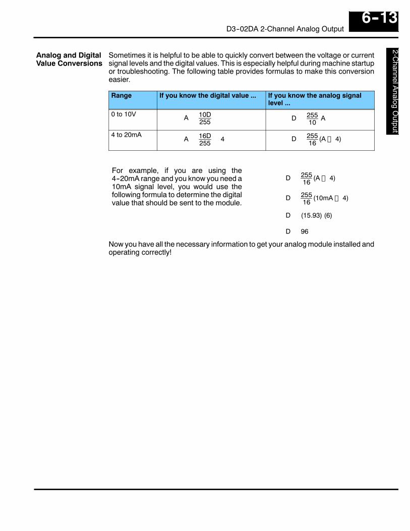
D3--02D
A2-C
hannelAnalog
Output
6--13D3--02DA 2-Channel Analog Output
Sometimes it is helpful to be able to quickly convert between the voltage or currentsignal levels and the digital values. This is especially helpful during machine startupor troubleshooting. The following table provides formulas to make this conversioneasier.
Range If you know the digital value ... If you know the analog signallevel ...
0 to 10V
4 to 20mA
For example, if you are using the4--20mA range and you know you need a10mA signal level, you would use thefollowing formula to determine the digitalvalue that should be sent to the module.
D = 25516
(A ≡ 4)
D = 25516
(10mA ≡ 4)
D = (15.93) (6)
D = 96
Now you have all the necessary information to get your analog module installed andoperating correctly!
Analog and DigitalValue Conversions
A = 10D255 D = 255
10A
A = 16D255 + 4 D = 255
16(A ≡ 4)

17F3--04DA--14-ChannelAnalog Output
In This Chapter. . . .— Module Specifications— Setting the Module Jumpers— Connecting the Field Wiring— Module Operation— Writing the Control Program

F3--0
4DA
--14-
Cha
nnel
Ana
log
Out
put
7--2F3--04DA--1 4-Channel Analog Output
Module Specifications
The following table provides the specifications for the F3--04DA--1 Analog OutputModule. Review these specifications to make sure the module meets yourapplication requirements.
Number of Channels 4
Output Ranges 0 -- 5V, 0 -- 10V, 4 -- 12 mA,4 -- 20 mA (source)
Resolution 12 bit (1 in 4096)
Output Type Single ended (one common)
Output Impedance 0.5O typical, voltage output
Output Current 5 mA source, 2.5 mA sink (voltage)
Short-circuit Current 40 mA typical, voltage output
Load Impedance 1KO maximum, current output2KO minimum, voltage output
Linearity Error ? 1 count (? 0.03% maximum)
Maximum Inaccuracy at 77 °F(25 °C)
? 0.6% of span, current output? 0.2% of span, voltage output
Accuracy vs. Temperature ? 50 ppm / _C maximum
Conversion Time 30µS maximum
Power Budget Requirement 144 mA @9V, 108 mA @ 24V
External Power Supply None required
Operating Temperature 32° to 140° F (0° to 60° C)
Storage Temperature --4° to 158° F (--20° to 70° C)
Relative Humidity 5 to 95% (non-condensing)
Environmental air No corrosive gases permitted
Vibration MIL STD 810C 514.2
Shock MIL STD 810C 516.2
Noise Immunity NEMA ICS3--304
The F3--04DA--1 Analog Output appears as a 16-point module. The module can beinstalled in any slot configured for 16 points. See the DL305 User Manual for detailson using 16 point modules in DL305 systems. The limitation on the number of analogmodules are:
S For local and expansion systems, the available power budget and16-point module usage are the limiting factors.
Analog OutputConfigurationRequirements

F3--04DA
--14-C
hannelAnalog
Output
7--3F3--04DA--1 4-Channel Analog Output
Setting the Module Jumpers
The module is set at the factory for a 0--10V signal on all four channels. (This rangealso allows 4--20 mA operation since there are separate I and V wiring terminals.) Ifthis is acceptable you do not have to change any of the jumpers. The followingdiagram shows the jumper locations.
Channel 25V10V
Channel 15V10V
Channel 45V10V
Channel 35V10V
Channel 2
Channel 1
Channel 4
Channel 3
The jumper is set from the factory to allow either 0--10V or 4--20mA operation on allchannels. In addition, you can select 0 -- 5V or 4 -- 12 mA operation by moving thejumper. (Only channel 1 is used in the example, but all channels must be set.)
Signal Range Jumper Settings
0 to +5 VDC4 to 12 mA
0 VDC to +10 VDC4 to 20 mA
Jumper Locations
Selecting OutputSignal Ranges
Range0--5V0--10V
Range0--5V0--10V
F3--0
4DA
--14-
Cha
nnel
Ana
log
Out
put
7--4F3--04DA--1 4-Channel Analog Output
Connecting the Field Wiring
Your company may have guidelines for wiring and cable installation. If so, you shouldcheck those before you begin the installation. Here are some general things toconsider.
S Use the shortest wiring route whenever possible.S Use shielded wiring and ground the shield at the module or the power
supply return (0V). Do not ground the shield at both the module and thetransducer.
S Don’t run the signal wiring next to large motors, high current switches, ortransformers. This may cause noise problems.
S Route the wiring through an approved cable housing to minimize the riskof accidental damage. Check local and national codes to choose thecorrect method for your application.
The F3--04DA--1 receives all power from the base. A separate power supply is notrequired.
Each channel can be wired independently for a voltage or current transducer.S Current transducers must have an impedance less than 1K ohm.S Voltage transducers must have an impedance greater than 2K ohms.
Wiring Guidelines
User Power SupplyRequirements
LoadRequirements

F3--04DA
--14-C
hannelAnalog
Output
7--5F3--04DA--1 4-Channel Analog Output
The F3--04DA--1 module has a removable connector to make wiring easier. Simplysqueeze the top and bottom tabs and gently pull the connector from the module.
ANALOG OUTPUTF3--04DA--1
COM
CH2
--I
+I
+ICH4
--I
COM
CH2
--V
+V
+VCH4
--V
CH1
--I
+I
+I
CH3
--I
CH1
--V
+V
+VCH3
--V
4--20mA are
CH1CH1
Current Sourcing
Voltage is Sink/Source
COM
CH2
--I
+I
+I
CH4
--I
COM
CH2
--V
+V
+V
CH4
--V
CH1
--I
+I
+I
CH3
--I
CH1
--V
+V
+VCH3
--V
CurrentOutput
0--1K ohm
CH3CurrentOutput
0--1K ohm
CH2VoltageOutput
2K ohm min
CH4VoltageOutput
2K ohm min
CH2
CH3
CH4
D/A
24VDCCOM
Note 1: Shields should be connected to the 0V (COM)of the module
Note 2: Unused voltage & current outputs should re-main open (no connections)
See Note 1
Internal Module Wiring
D/A
D/A
D/A
RemovableConnector
Wiring Diagram

F3--0
4DA
--14-
Cha
nnel
Ana
log
Out
put
7--6F3--04DA--1 4-Channel Analog Output
Module Operation
Before you begin writing the control program, it is important to take a few minutes tounderstand how the module processes and represents the analog signals.The F3--04DA--1 module can update one channel per CPU scan. Your RLL programselects which channel to update, so you have complete flexibility to solve yourapplication requirements.
Channel 1 Scan N
Calculate the data
Write data
I/O Update
Execute Application ProgramChannel 3 Scan N+1
Channel 1 Scan N+2
Channel 4 Scan N+3
Scan N+4
Scan
Channel 2
Channel ScanningSequence

F3--04DA
--14-C
hannelAnalog
Output
7--7F3--04DA--1 4-Channel Analog Output
You may recall the F3--04DA--1 module appears to the CPU as a 16-point module.These 16 points provide:
S the digital representation of the analog signal.S identification of the channel to receive the data.
Since all I/O points are automatically mapped into Register (R) memory, it is veryeasy to determine the location of the data word that will be assigned to the module.
110
F3--04DA1
R 011MSB LSB
R 001MSB LSB
010
R 002, R012 R 000, R010
117
8ptRelay
8ptOutput
16ptInput
16pt(Analog)
4ch.Input
8ptOutput
050--
057
040--
047
030--
037
020027
--120127
000007
--100107
010017
--110117
017
Within these two word locations, the individual bits represent specific informationabout the analog signal.
The last four points of the upper registerare used as outputs to tell the modulewhich channel to update. In our example,when output 114 is on, channel 1 will beupdated. Here’s how the outputs areassigned.Output Channels114 1115 2116 3117 4
R011MSB LSB
110
117
116
115
114
113
112
111
-- channel selection outputs
Understanding theI/O Assignments
Channel SelectionInputs

F3--0
4DA
--14-
Cha
nnel
Ana
log
Out
put
7--8F3--04DA--1 4-Channel Analog Output
The remaining twelve bits represent theanalog data in binary format.Bit Value Bit Value0 (LSB) 1 6 641 2 7 1282 4 8 2563 8 9 5124 16 10 10245 32 11 2048
117
R001MSB LSB
010
116
115
114
113
112
111
110
017
016
015
014
013
012
011
-- data bits
R011
Since the module has 12-bit resolution, the analog signal is converted into 4096“pieces” ranging from 0 -- 4095 (212). For example, with a 0 to 10V scale, a 0V signalwould be 0, and a 10V signal would be 4095. This is equivalent to a a binary value of0000 0000 0000 to 1111 1111 1111, or 000 to FFF hexadecimal. The followingdiagram shows how this relates to each signal range.
+V
0V0 4095
0V -- 10V0V -- 5V
12mA
4 mA
0 4095
4 -- 12mA
20mA
4mA
0 4095
4 -- 20mA
Each “piece” can also be expressed interms of the signal level by using theequation shown. The following tableshows the smallest signal levels that willpossibly result in a change in the datavalue for each signal range.
Resolution = H ≡ L4095
H = high limit of the signal rangeL = low limit of the signal range
Range Highest Signal Lowest Signal Smallest Change
0 to 5V 5V 0V 1.22 mV
0 to 10V 10V 0V 2.44 mV
4 to 12mA 12mA 4mA 1.95 µA
4 to 20mA 20mA 4mA 3.91 µA
Now that you understand how the module and CPU work together to gather andstore the information, you’re ready to write the control program.
Analog Data Bits

F3--04DA
--14-C
hannelAnalog
Output
7--9F3--04DA--1 4-Channel Analog Output
Writing the Control Program
As mentioned earlier, you can use the channel selection bits to determine whichchannels will be updated. The following diagram shows the location for both thechannel selection bits and data bits.
F3--04DA--1
R 011MSB LSB
R 001MSB LSB
010
R 002, R012 R 000, R010
8ptRelay
8ptOutput
16ptInput
16pt(Analog)
4ch.Input
8ptOutput
050--
057
040--
047
030--
037
020027
--120127
000007
--100107
010017
--110117
017
117
116
115
114
110
-- data bits-- channel selection inputs
Your program has to calculate the digitalvalue to send to the analog module.There are many ways to do this, but mostall applications are understood moreeasily if you use measurements inengineering units. This is accomplishedby using the conversion formula shown.You may have to make adjustments tothe formula depending on the scale youchoose for the engineering units.
A = 4096 UH ≡ L
A = Analog value (0 -- 4095)U = Engineering UnitsH = high limit of the Engineering
unit rangeL = low limit of the Engineering
unit range
The following example shows how you would use Engineering units to obtain thedigital value to represent pressure (PSI) from 0 to 100. This example assumes youwant to obtain a pressure of 42 PSI, which is slightly less than half scale.
A = 4096 UH ≡ L
A = 1720
A = 4096 42100 ≡ 0
Identifying theData Locations
Calculating theDigital Value
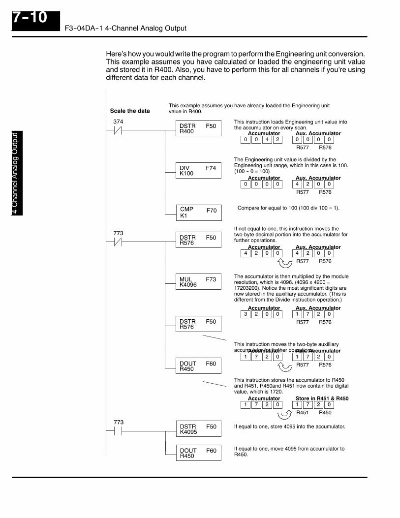
F3--0
4DA
--14-
Cha
nnel
Ana
log
Out
put
7--10F3--04DA--1 4-Channel Analog Output
Here’s how you would write the program to perform the Engineering unit conversion.This example assumes you have calculated or loaded the engineering unit valueand stored it in R400. Also, you have to perform this for all channels if you’re usingdifferent data for each channel.
374DSTRR400
F50
DIVK100
F74
This instruction loads Engineering unit value intothe accumulator on every scan.
If not equal to one, this instruction moves thetwo-byte decimal portion into the accumulator forfurther operations.
Scale the data
The Engineering unit value is divided by theEngineering unit range, which in this case is 100.(100 -- 0 = 100)
DSTRR576
F50
MULK4096
F73
DSTRR576
F50
DOUTR450
F60
0 0 4 2Accumulator
0 0 0 0Aux. Accumulator
0 0 0 0Accumulator
4 2 0 0Aux. Accumulator
This example assumes you have already loaded the Engineering unitvalue in R400.
4 2 0 0Accumulator
4 2 0 0Aux. Accumulator
The accumulator is then multiplied by the moduleresolution, which is 4096. (4096 x 4200 =17203200). Notice the most significant digits arenow stored in the auxilliary accumulator. (This isdifferent from the Divide instruction operation.)
3 2 0 0Accumulator
1 7 2 0Aux. Accumulator
R577 R576
R577 R576
R577 R576
R577 R576
This instruction moves the two-byte auxilliaryaccumulator for further operations.
1 7 2 0Accumulator
1 7 2 0Aux. Accumulator
R577 R576
This instruction stores the accumulator to R450and R451. R450and R451 now contain the digitalvalue, which is 1720.
1 7 2 0Accumulator
1 7 2 0Store in R451 & R450
R451 R450
CMPK1
F70 Compare for equal to 100 (100 div 100 = 1).
773
DSTRK4095
F50
DOUTR450
F60
773If equal to one, store 4095 into the accumulator.
If equal to one, move 4095 from accumulator toR450.

F3--04DA
--14-C
hannelAnalog
Output
7--11F3--04DA--1 4-Channel Analog Output
There will probably be times when you need more precise control. For example,maybe your application requires 42.9 PSI, not just 42 PSI. By changing the scalingvalue slightly, we can “imply” an extra decimal of precision. Notice in the followingexample we’ve entered 429 as the Engineering unit value and we’ve added anotherdigit to the scale. Instead of a scale of 100, we’re using 1000, which implies 100.0 forthe PSI range.
374DSTRR400
F50
DIVK1000
F74
This instruction loads Engineering unit value intothe accumulator on every scan.
If not equal to one, this instruction moves thetwo-byte decimal portion into the accumulator forfurther operations.
Scale the data
The Engineering unit value is divided by theEngineering unit range, which in this case is 1000.(100.0 implied range)
DSTRR576
F50
MULK4096
F73
DSTRR576
F50
DOUTR450
F60
0 4 2 9Accumulator
0 0 0 0Aux. Accumulator
0 0 0 0Accumulator
4 2 9 0Aux. Accumulator
This example assumes you have already loaded the Engineering unitvalue in R400.
4 2 9 0Accumulator
4 2 9 0Aux. Accumulator
The accumulator is then multiplied by the moduleresolution, which is 4096. (4096 x 4290 =17571840). Notice the most significant digits arenow stored in the auxilliary accumulator. (This isdifferent from the Divide instruction operation.)
1 8 4 0Accumulator
1 7 5 7Aux. Accumulator
R577 R576
R577 R576
R577 R576
R577 R576
This instruction moves the two-byte auxilliaryaccumulator for further operations.
1 7 5 7Accumulator
1 7 5 7Aux. Accumulator
R577 R576
This instruction stores the accumulator to R450and R451. R450 and R451 now contain the digitalvalue, which is 1757.
1 7 5 7Accumulator
1 7 5 7Store in R451 & R450
R451 R450
CMPK1
F70 Compare for equal to 1000 (1000 div 1000 = 1).
DSTRK4095
F50
DOUTR450
F60
773 If equal to one, store 4095 into the accumulator.
If equal to one, move 4095 from accumulator toR450.
773

F3--0
4DA
--14-
Cha
nnel
Ana
log
Out
put
7--12F3--04DA--1 4-Channel Analog Output
The following program example shows how to send the digital value to a singlechannel.
374DSTRR450
F50
Send Channel 1
This rung loads the data into the accumulator onevery scan.
BIN F85Since the data is in BCD format, you have toconvert it to binary before you send the data to themodule.
DOUT5R001
F65Send the accumulator data to the Register thatcorresponds to the module, which is R001.
Indicate the channel to update. In this case,channel 1 is being updated.
This example assumes you have already loaded the Engineering unit value in R450 and R451.
OUT114
To update other channels with the same outputdata, simple add the channel selection outputs forthe additional channels.
OUT115
If you install the F3--04DA--1 in the slot corresponding to registers 6 and 16, you haveto make a slight program adjustment. This is because the DOUT5 instruction is notsupported for this slot.
374DSTRR450
F50
Send Channel 1
This rung loads the data into the accumulator onevery scan.
BIN F85Since the data is in BCD format, you have toconvert it to binary before you send the data to themodule.
DOUT1R006
F61Send the 8 least significant data bits to the firstRegister that corresponds to the module which isR006.
Indicate the channel to update. In this case,channel 1 is being updated.
This example assumes you have already loaded the Engineering unit value in R450 and R451.
OUT164
SHFRK0008
F80
DOUT3R016
F63
Shift the 4 most significant data bits to the right 8places. (The data is still in the accumulator).
Send the 4 most significant data bits to the secondRegister that corresponds to the module which isR016.
Sending Data to aSingle Channel

F3--04DA
--14-C
hannelAnalog
Output
7--13F3--04DA--1 4-Channel Analog Output
This example shows how to send digital values to the module when you have morethan one channel. This example will automatically update all four channels over fourscans. The example is fairly simple and will work in most all situations, but there areinstances where problems can occur. The logic must be active on the first CPU scanand all subsequent scans. If the logic gets stopped or disabled for some reason,there is no way to restart it. If you’re using an RLLPLUS (Stage) program, put this logicin an initial stage that is always active. Also, you should avoid using the this exampleif you require the analog output logic to be used inside a Master Control Relay field ofcontrol. Even if you do not have a need for the MCR, you can still accidentally disablethe analog output logic by inadvertently writing to the multiplexing control relays withan operator interface or intelligent module, such as an ASCII BASIC module, etc.The following program example shows how to send the digital values to multiplechannels. With this program, all channels will be updated within four scans. You mustuse the rungs in the order shown, but you can include them anywhere in the program.
When channel 4 has been updated, 160 restartsthe update sequence.
When channel 3 has been updated, this rung loadsthe data for channel 4 into the accumulator. Byturning on 117, this triggers the channel update.(Since 117 is also used as an input, this results ina one-shot.)
374
117OUT RST
160Ch4 Done
116DSTRR456
F50
Ch3 Done
OUT117
115Ch2 Done
114Ch1 Done
160Restart
374 OnFirstScan
When channel 2 has been updated, this rung loadsthe data for channel 3 into the accumulator. Byturning on 116, this triggers the channel update.(Since 116 is also used as an input, this results ina one-shot.)
When channel 1 has been updated, this rung loadsthe data for channel 2 into the accumulator. Byturning on 115, this triggers the channel update.(Since 115 is also used as an input, this results ina one-shot.)
This rung loads the data for channel 1 into theaccumulator. Since 374 is used, this rungautomatically executes on the first scan. After that,160 restarts this rung. If you examine the first rung,you’ll notice 160 only comes on after channel 4has been updated.
DSTRR454
F50
OUT116
DSTRR452
F50
OUT115
DSTRR450
F50
OUT114
Alwayson
Since the data is in BCD format, you have toconvert it to binary before you send the data to themodule. (You can omit this step if you’ve alreadyconverted the data elsewhere.)
BIN F85
DOUT1R001
F61
SHFRK 8
F80
DOUT3R0011
F63
Send the 8 least significant data bits to the firstRegister that corresponds to the module which isR001.
Shift the 4 most significant data bits to the right 8places. (The data is still in the accumulator).
Send the 4 most significant data bits to the secondRegister that corresponds to the module which isR011.
Sequencing theChannel Updates
SequencingExample

F3--0
4DA
--14-
Cha
nnel
Ana
log
Out
put
7--14F3--04DA--1 4-Channel Analog Output
Sometimes it is helpful to be able to quickly convert between the voltage or currentsignal levels and the digital values. This is especially helpful during machine startupor troubleshooting. The following table provides formulas to make this conversioneasier.
Range If you know the digital value ... If you know the analog signallevel ...
0 to 5V
0 to 10V
4 to 12mA
4 to 20mA
For example, if you are using the4--20mA range and you know you need a10mA signal level, you would use thefollowing formula to determine the digitalvalue that should be sent to the module.
D = 409516
(A ≡ 4)
D = 409516
(10mA ≡ 4)
D = (255.93) (6)
D = 1536
Now you have all the necessary information to get your analog module installed andoperating correctly!
Analog and DigitalValue Conversions
A = 5D4095 D = 4095
5A
A = 10D4095 D = 4095
10A
A = 12D4095 + 4 D = 4095
12(A ≡ 4)
A = 16D4095 + 4 D = 4095
16(A ≡ 4)
18F3--04DAS4-Channel IsolatedAnalog Output
In This Chapter. . . .— Module Specifications— Setting the Module Jumpers— Connecting the Field Wiring— Module Operation— Writing the Control Program

F3--0
4DA
S4
Ch.
Isol
ated
Ana
log
Out
.8--2
F3--04DAS 4-Channel Isolated Analog Output
Module Specifications
The following table provides the specifications for the F3--04DAS Analog OutputModule. Review these specifications to make sure the module meets yourapplication requirements.
Number of Channels 4
Output Ranges ? 5V, ? 10V, 0--5V, 0--10V, 1--5V,0--20 mA, 4--20 mA
Resolution 12 bit (1 in 4096)
Output Type Isolated, 750 VDC channel-to-channel750 VDC channel-to-logic
Output Current ? 5 mA, voltage output
Short-circuit Current ? 20 mA typical, voltage output
Capacitive Load Drive 0.1µF typical, voltage output
Load Impedance 470O maximum, current output2KO minimum, voltage output
Isolation Mode Rejection 140 dB at 60Hz
Linearity Error ? 1 count (? 0.03% maximum)
Calibration Error ? 0.15% typical, ? 0.75% maximum of span? 10 ppm / _C maximum of full scale
Calibrated Offset Error ? 1 count maximum, current output? 5 mV typical, ? 50 mV max., voltage output? 0.2 mV typical / _C
Conversion Time 30µS maximum, 1 channel/scan
Power Budget Requirement 154 mA @9V, 145 mA @ 24V (maximum)
External Power Supply None required
Operating Temperature 32° to 140° F (0° to 60° C)
Storage Temperature --4° to 158° F (--20° to 70° C)
Relative Humidity 5 to 95% (non-condensing)
Environmental air No corrosive gases permitted
Vibration MIL STD 810C 514.2
Shock MIL STD 810C 516.2
Noise Immunity NEMA ICS3--304

F3--04DA
S4
Ch.Isolated
Analog
Out.
8--3F3--04DAS 4-Channel Isolated Analog Output
The F3--04DAS Analog Output appears as a 16-point module. The module can beinstalled in any slot configured for 16 points, but should not be installed in Slot 3 ofany DL305 base. See the DL305 User Manual for details on using 16 point modulesin DL305 systems. The limitation on the number of analog modules are:
S For local and expansion systems, the available power budget and16-point module usage are the limiting factors.
WARNING: You should not install this module in Slot 3 of any DL305 base. Themodule has traces on the edge card connector that may become damaged ifthe module is repeatedly installed and removed. The solder mask thatprotects the traces may be scraped off, which may cause a short circuit on theI/O bus. The short circuit can lead to unpredictable system operation or causedamage to the CPU or power supply.
DL305CPU
0123
DL305CPU
0123456
DL305CPU
0123456710or70
Analog OutputConfigurationRequirements

F3--0
4DA
S4
Ch.
Isol
ated
Ana
log
Out
.8--4
F3--04DAS 4-Channel Isolated Analog Output
Setting the Module Jumpers
The module is set at the factory for a 0--10V signal on all four channels. If this isacceptable you do not have to change any of the jumpers.If you examine the top board on the module you will notice four sets of jumpers. Thejumpers are assigned to the channels as follows.
S Channel 1 — Jumper JP4S Channel 2 — Jumper JP3S Channel 3 — Jumper JP2S Channel 4 — Jumper JP1
NOTE: At first glance it might appear we have the channel / jumper assignments outof order. Your eyes do not deceive you. Channel 1 is controlled by JP4.
Each channel also has a jumper located on the bottom board of the module. Thesejumpers select a 1V (or 4mA) offset for each channel. Remove the jumper for anyrange that requires an offset. These jumpers are assigned as expected. JP1 selectsan offset for channel 1, JP2 selects an offset for channel 2, etc.The following diagram shows how the jumpers are assigned. It also shows thefactory settings.
1
Channel 1 Range
1
Channel 2 Ranges
1
Channel 3 Ranges
1
Channel 4 Ranges
Channel 1 Offset
JP4
JP3
JP2
JP1
JP1
Channel 2 Offset
JP2
Channel 3 Offset
JP3
Channel 4 Offset
JP4
Jumper Locations

F3--04DA
S4
Ch.Isolated
Analog
Out.
8--5F3--04DAS 4-Channel Isolated Analog Output
The following tables show the jumper selections for the various ranges. (Onlychannel 1 is used in the example, but all channels must be set.)
Bipolar Signal Range Jumper Settings
--5 VDC to +5 VDC
--10 VDC to +10 VDC
Unipolar Signal Range Jumper Settings
4 to 20 mA(1 VDC to 5 VDC)
0 VDC to +5 VDC(0 to +20 mA)
0 VDC to +10 VDC
Selecting InputSignal Ranges
Offset Jumper (JP1)
1
Channel 1 (JP4)
Offset Jumper (JP1)
1
Channel 1 (JP4)
Offset Jumper (JP1)
1
Channel 1 (JP4)
Offset Jumper (JP1)
1
Channel 1 (JP4)
Offset Jumper (JP1)
1
Channel 1 (JP4)

F3--0
4DA
S4
Ch.
Isol
ated
Ana
log
Out
.8--6
F3--04DAS 4-Channel Isolated Analog Output
The following tables show the jumper selections for some additional ranges that arenot normally found in many applications. Notice you can install or remove the offsetjumper to change the settings. (Only channel 1 is used in the example, but allchannels must be set.)
Signal RangeOffset Installed
Signal RangeOffset Removed
Jumper Settings
--10 VDC to +6 VDC --9 VDC to +7 VDC
--5 VDC to +3 VDC --4 VDC to +4 VDC
--2.5 VDC to+2.5 VDC
--1.5 VDC to+3.5 VDC
--2.5 VDC to+1.5 VDC
--1.5 VDC to+2.5 VDC
0 VDC to 8 VDC 1 VDC to 9 VDC
0 VDC to 4 VDC 1 VDC to 5 VDC
Special OutputSignal Ranges
1
Channel 1 (JP4)
1
Channel 1 (JP4)
1
Channel 1 (JP4)
1
Channel 1 (JP4)
1
Channel 1 (JP4)
1
Channel 1 (JP4)

F3--04DA
S4
Ch.Isolated
Analog
Out.
8--7F3--04DAS 4-Channel Isolated Analog Output
Connecting the Field Wiring
Your company may have guidelines for wiring and cable installation. If so, you shouldcheck those before you begin the installation. Here are some general things toconsider.
S Use the shortest wiring route whenever possible.S Use shielded wiring and ground the shield at the module or the power
supply return (0V). Do not ground the shield at both the module and thetransducer.
S Don’t run the signal wiring next to large motors, high current switches, ortransformers. This may cause noise problems.
S Route the wiring through an approved cable housing to minimize the riskof accidental damage. Check local and national codes to choose thecorrect method for your application.
The F3--04DAS receives all power from the base. A separate power supply is notrequired.
Each channel can be wired independently for a voltage or current transducer.S Current transducers must have an impedance less than 470 ohms.S Voltage transducers must have an impedance greater than 2K ohms.
Wiring Guidelines
User Power SupplyRequirements
LoadRequirements

F3--0
4DA
S4
Ch.
Isol
ated
Ana
log
Out
.8--8
F3--04DAS 4-Channel Isolated Analog Output
The F3--04DAS module has a removable connector to make wiring easier. Simplysqueeze the top and bottom tabs and gently pull the connector from the module.
ANALOG OUTPUTF3--04DAS
CH1--V
+V
+VCH2--V
CH3--V
+V
+VCH4--V
CH1--I
+I
+ICH2--I
CH3--I
+I
+ICH4--I
CH1
Voltage
--V
+V
+V
--V
--V
+V
+V
--V
CH1--I
+I
+I
CH2--I
CH3
--I
+I
+ICH4
--I
CurrentOutput
0--470 ohm
CH2CurrentOutput
0--470ohm
CH3VoltageOutput
2K ohm min
CH4VoltageOutput
2K ohm min
Note1: Shields should be connected to the respective channel’s-- V terminal of the module.
Note 2: Each isolated output channel may have either a voltage orcurrent load, but not both
Note 3: An external 0.31 Amp fast-acting fuse in series with the isolated+I terminal (+15VDC) is recommended to protect against accidentalshorts to the --V terminal (15VDC common)
Note 4: Do not attempt to source more than 20mA from any one of thefour isolated +15VDC power supplies
Output
CurrentSink
15VDC (20mA)Isolated Power
VoltageOutput
CurrentSink
15VDC (20mA)Isolated Power
CH1
CH4
Internal wiring for CH2 & 3 issimilar to wiring shown above
See note
Internal Module Wiring
You may occasionally encounter transmitters that have a very unusual signal range.Since each channel is isolated, you can “daisy chain” the channels to provide outputvoltage signals that are outside of the normal operating range. For example, youcould connect the first two channels to provide a voltage output from 0 to 20 VDC.
2K ohm minUser Load
0--20V
+V
CH1
--V
+V
CH2
--V
0--10
CH1 & 2are configured
for 0--10V
0--10
RemovableConnector
Wiring Diagram
Combining VoltageOutputs

F3--04DA
S4
Ch.Isolated
Analog
Out.
8--9F3--04DAS 4-Channel Isolated Analog Output
You cannot connect the current outputs in series (like the voltage outputs) but youcan achieve unusual ranges with a few wiring and programming tricks. For example,let’s say an application requires a ? 20 mA range. By completing the following steps,you could easily accommodate this requirement.
1. Configure channel 1 and channel 2 for 0--20mA.2. Connect the +I of channel 1 to the --I of channel 2.3. Connect the --I of channel 1 to the +I of channel 2.4. Send 0 (digital value) to channel 2 while you send 0--4095 (digital value) to
channel 1. To reverse the power flow, send 0 to channel 1 while you sendthe 0--4095 value to channel 2. (See the section on Writing the ControlProgram for information on sending data values.)
WARNING: The isolated +15 VDC power supplies are rated at a maximum of 20mA. Current ratings that exceed 20 mA will damage the module beyond repair.For example, if you used the 0--10 VDC range for the example, the currentwould approach 40 mA which would cause damage to the module.
0--470 ohmUser Load
+/-- 20mA
+I
CH1
--I
+I
CH2
--I
0--20mA
CH1 & 2are configured
for 0--20mA
0--20mA
Combining CurrentOutputs
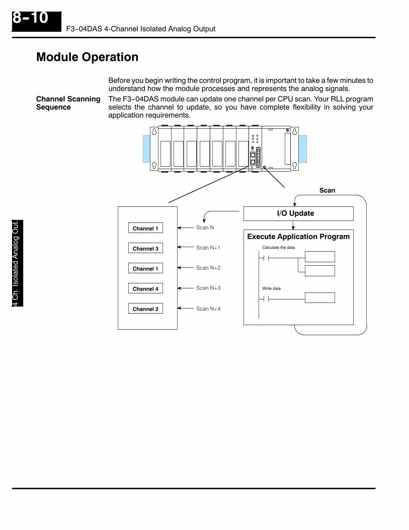
F3--0
4DA
S4
Ch.
Isol
ated
Ana
log
Out
.8--10
F3--04DAS 4-Channel Isolated Analog Output
Module Operation
Before you begin writing the control program, it is important to take a few minutes tounderstand how the module processes and represents the analog signals.The F3--04DAS module can update one channel per CPU scan. Your RLL programselects the channel to update, so you have complete flexibility in solving yourapplication requirements.
Channel 1 Scan N
Calculate the data
Write data
I/O Update
Execute Application ProgramChannel 3 Scan N+1
Channel 1 Scan N+2
Channel 4 Scan N+3
Scan N+4
Scan
Channel 2
Channel ScanningSequence
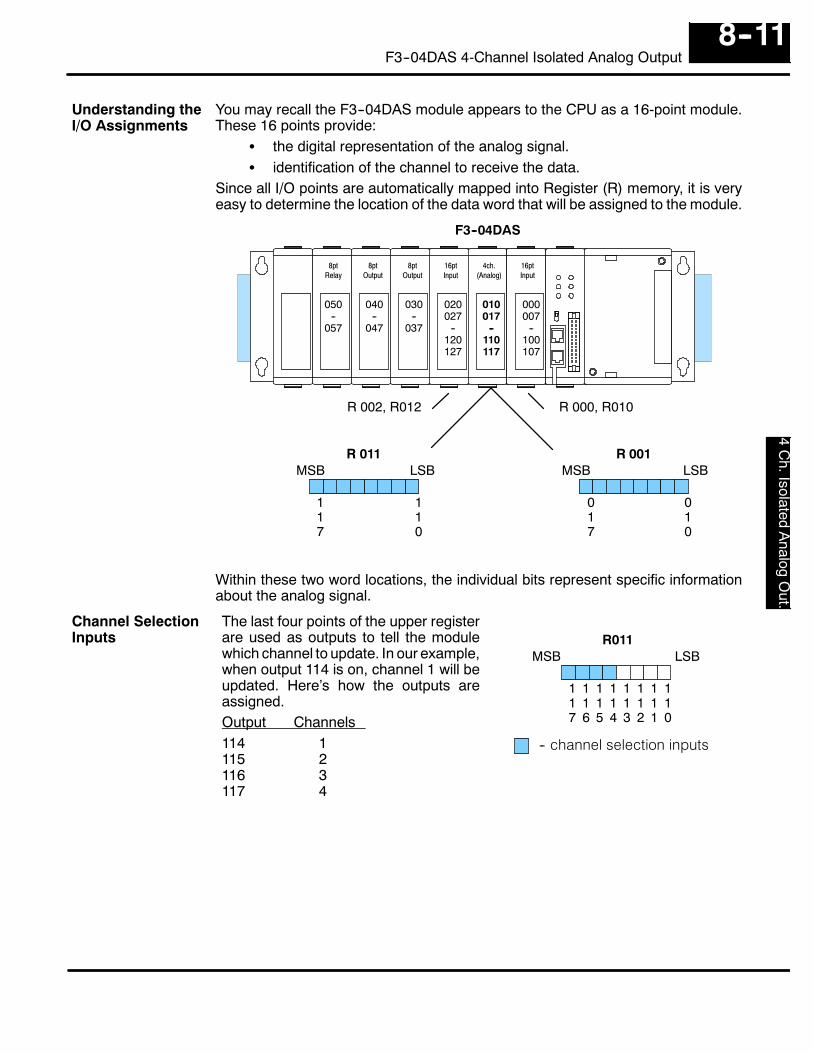
F3--04DA
S4
Ch.Isolated
Analog
Out.
8--11F3--04DAS 4-Channel Isolated Analog Output
You may recall the F3--04DAS module appears to the CPU as a 16-point module.These 16 points provide:
S the digital representation of the analog signal.S identification of the channel to receive the data.
Since all I/O points are automatically mapped into Register (R) memory, it is veryeasy to determine the location of the data word that will be assigned to the module.
110
F3--04DAS
R 011MSB LSB
R 001MSB LSB
010
R 002, R012 R 000, R010
117
8ptRelay
8ptOutput
16ptInput
16pt(Analog)
4ch.Input
8ptOutput
050--
057
040--
047
030--
037
020027
--120127
000007
--100107
010017
--110117
017
Within these two word locations, the individual bits represent specific informationabout the analog signal.
The last four points of the upper registerare used as outputs to tell the modulewhich channel to update. In our example,when output 114 is on, channel 1 will beupdated. Here’s how the outputs areassigned.Output Channels114 1115 2116 3117 4
R011MSB LSB
110
117
116
115
114
113
112
111
-- channel selection inputs
Understanding theI/O Assignments
Channel SelectionInputs

F3--0
4DA
S4
Ch.
Isol
ated
Ana
log
Out
.8--12
F3--04DAS 4-Channel Isolated Analog Output
The remaining twelve bits represent theanalog data in binary format.Bit Value Bit Value0 (LSB) 1 6 641 2 7 1282 4 8 2563 8 9 5124 16 10 10245 32 11 2048
117
R001MSB LSB
010
116
115
114
113
112
111
110
017
016
015
014
013
012
011
-- data bits
R011
Since the module has 12-bit resolution, the analog signal is converted into 4096“pieces” ranging from 0 -- 4095 (212). For example, with a 0 to 10V scale, a 0V signalwould be 0, and a 10V signal would be 4095. This is equivalent to a a binary value of0000 0000 0000 to 1111 1111 1111, or 000 to FFF hexadecimal. The followingdiagram shows how this relates to each signal range.
+V
0V
--V0 4095
--10V -- +10V--5V -- +5V
+V
0V0 4095
0V -- 10V0V -- 5V
+5V
1V
0 4095
1V -- 5V
20mA
4mA
0 4095
4 -- 20mA
Each “piece” can also be expressed interms of the signal level by using theequation shown. The following tableshows the smallest signal levels that willpossibly result in a change in the datavalue for each signal range.
Resolution = H ≡ L4095
H = high limit of the signal rangeL = low limit of the signal range
Range Highest Signal Lowest Signal Smallest Change
--10 to +10V +10V --10V 4.88 mV
--5 to +5V +5 V --5V 2.44 mV
0 to 5V 5V 0V 1.22 mV
0 to 10V 10V 0V 2.44 mV
1 to 5V 5V 1V 0.98 mV
4 to 20mA 20mA 4mA 3.91 µA
Now that you understand how the module and CPU work together to gather andstore the information, you’re ready to write the control program.
Analog Data Bits

F3--04DA
S4
Ch.Isolated
Analog
Out.
8--13F3--04DAS 4-Channel Isolated Analog Output
Writing the Control Program
As mentioned earlier, you can use the channel selection bits to determine whichchannels will be updated. The following diagram shows the location for both thechannel selection bits and data bits.
F3--04DAS
R 011MSB LSB
R 001MSB LSB
010
R 002, R012 R 000, R010
8ptRelay
8ptOutput
16ptInput
16pt(Analog)
4ch.Input
8ptOutput
050--
057
040--
047
030--
037
020027
--120127
000007
--100107
010017
--110117
017
110
117
116
115
114
-- channel selection inputs-- data bits
Your program has to calculate the digitalvalue to send to the analog module.There are many ways to do this, but mostall applications are understood moreeasily if you use measurements inengineering units. This is accomplishedby using the conversion formula shown.You may have to make adjustments tothe formula depending on the scale youchoose for the engineering units.
A = 4096 UH ≡ L
A = Analog value (0 -- 4095)U = Engineering UnitsH = high limit of the Engineering
unit rangeL = low limit of the Engineering
unit range
The following example shows how you would use Engineering Units to obtain thedigital value to represent pressure (PSI) from 0 to 100. This example assumes youwant to obtain a pressure of 42 PSI, which is slightly less than half scale.
A = 4096 UH ≡ L
A = 1720
A = 4096 42100 ≡ 0
Identifying theData Locations
Calculating theDigital Value

F3--0
4DA
S4
Ch.
Isol
ated
Ana
log
Out
.8--14
F3--04DAS 4-Channel Isolated Analog Output
Here’s how you would write the program to perform the Engineering Unit conversion.This example assumes you have calculated or loaded the engineering unit valueand stored it in R400. Also, you have to perform this for all channels if you’re usingdifferent data for each channel.
374DSTRR400
F50
DIVK100
F74
This instruction loads Engineering unit value intothe accumulator on every scan.
This instruction moves the two-byte decimalportion into the accumulator for further operations.
Scale the data
The Engineering unit value is divided by theEngineering unit range, which in this case is 100.(100 -- 0 = 100)
DSTRR576
F50
MULK4096
F73
DSTRR576
F50
DOUTR450
F60
0 0 4 2Accumulator
0 0 0 0Aux. Accumulator
0 0 0 0Accumulator
4 2 0 0Aux. Accumulator
This example assumes you have already loaded the Engineering unitvalue in R400.
4 2 0 0Accumulator
4 2 0 0Aux. Accumulator
The accumulator is then multiplied by the moduleresolution, which is 4096. (4096 x 4200 =17203200). Notice the most significant digits arenow stored in the auxilliary accumulator. (This isdifferent from the Divide instruction operation.)
3 2 0 0Accumulator
1 7 2 0Aux. Accumulator
R577 R576
R577 R576
R577 R576
R577 R576
This instruction moves the two-byte auxilliaryaccumulator for further operations.
1 7 2 0Accumulator
1 7 2 0Aux. Accumulator
R577 R576
This instruction stores the accumulator to R450and R451. R450 and R451 now contain the digitalvalue, which is 1720.
1 7 2 0Accumulator
1 7 2 0Store in R451 & R450
R451 R450
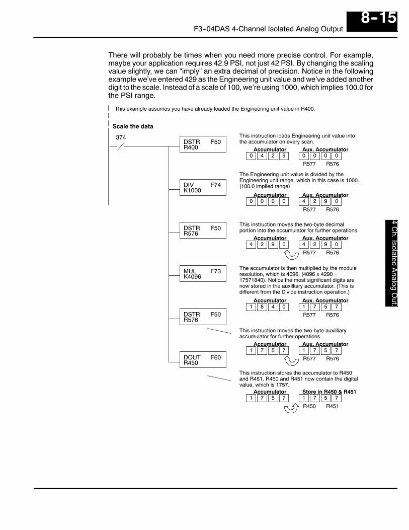
F3--04DA
S4
Ch.Isolated
Analog
Out.
8--15F3--04DAS 4-Channel Isolated Analog Output
There will probably be times when you need more precise control. For example,maybe your application requires 42.9 PSI, not just 42 PSI. By changing the scalingvalue slightly, we can “imply” an extra decimal of precision. Notice in the followingexample we’ve entered 429 as the Engineering unit value and we’ve added anotherdigit to the scale. Instead of a scale of 100, we’re using 1000, which implies 100.0 forthe PSI range.
374DSTRR400
F50
DIVK1000
F74
This instruction loads Engineering unit value intothe accumulator on every scan.
This instruction moves the two-byte decimalportion into the accumulator for further operations.
Scale the data
The Engineering unit value is divided by theEngineering unit range, which in this case is 1000.(100.0 implied range)
DSTRR576
F50
MULK4096
F73
DSTRR576
F50
DOUTR450
F60
0 4 2 9Accumulator
0 0 0 0Aux. Accumulator
0 0 0 0Accumulator
4 2 9 0Aux. Accumulator
This example assumes you have already loaded the Engineering unit value in R400.
4 2 9 0Accumulator
4 2 9 0Aux. Accumulator
The accumulator is then multiplied by the moduleresolution, which is 4096. (4096 x 4290 =17571840). Notice the most significant digits arenow stored in the auxilliary accumulator. (This isdifferent from the Divide instruction operation.)
1 8 4 0Accumulator
1 7 5 7Aux. Accumulator
R577 R576
R577 R576
R577 R576
R577 R576
This instruction moves the two-byte auxilliaryaccumulator for further operations.
1 7 5 7Accumulator
1 7 5 7Aux. Accumulator
R577 R576
This instruction stores the accumulator to R450and R451. R450 and R451 now contain the digitalvalue, which is 1757.
1 7 5 7Accumulator
1 7 5 7Store in R450 & R451
R450 R451

F3--0
4DA
S4
Ch.
Isol
ated
Ana
log
Out
.8--16
F3--04DAS 4-Channel Isolated Analog Output
The following program example shows how to send the digital value to a singlechannel.
374DSTRR450
F50
Send Channel 1
This rung loads the data into the accumulator onevery scan.
BIN F85Since the data is in BCD format, you have toconvert it to binary before you send the data to themodule.
DOUT5R001
F65Send the accumulator data to the Register thatcorresponds to the module, which is R001.
Indicate the channel to update. In this case,channel 1 is being updated.
This example assumes you have already loaded the Engineering unit value in R450 and R451.
OUT114
To update other channels with the same outputdata, simple add the channel selection outputs forthe additional channels.
OUT115
If you install the F3--04DA--1 in the slot corresponding to registers 6 and 16, you haveto make a slight program adjustment. This is because the DOUT5 instruction is notsupported for this slot.
374DSTRR450
F50
Send Channel 1
This rung loads the data into the accumulator onevery scan.
BIN F85Since the data is in BCD format, you have toconvert it to binary before you send the data to themodule.
DOUT1R006
F61Send the 8 least significant data bits to the firstRegister that corresponds to the module which isR006.
Indicate the channel to update. In this case,channel 1 is being updated.
This example assumes you have already loaded the Engineering unit value in R450 and R451.
OUT164
SHFRK0008
F80
DOUT3R016
F63
Shift the 4 most significant data bits to the right 8places. (The data is still in the accumulator).
Send the 4 most significant data bits to the secondRegister that corresponds to the module which isR016.
Sending Data to aSingle Channel

F3--04DA
S4
Ch.Isolated
Analog
Out.
8--17F3--04DAS 4-Channel Isolated Analog Output
This example shows how to send digital values to the module when you have morethan one channel. This example will automatically update all four channels over fourscans. The example is fairly simple and will work in most all situations, but there areinstances where problems can occur. The logic must be active on the first CPU scanand all subsequent scans. If the logic gets stopped or disabled for some reason,there is no way to restart it. If you’re using an RLLPLUS (Stage) program, put this logicin an initial stage that is always active. Also, you should avoid using the this exampleif you require the analog output logic to be used inside a Master Control Relay field ofcontrol. You could also accidentally disable the analog output logic by inadvertentlywriting to the multiplexing control relays with an operator interface or intelligentmodule, such as an ASCII BASIC module, etc.The following program example shows how to send the digital values to multiplechannels. With this program, all channels will be updated within four scans. You mustuse the rungs in the order shown, but you can include them anywhere in the program.
When channel 4 has been updated, 160 restartsthe update sequence.
When channel 3 has been updated, this rung loadsthe data for channel 4 into the accumulator. Byturning on 117, this triggers the channel update.(Since 117 is also used as an input, this results ina one-shot.)
374
117OUT160
Ch4 Done
116DSTRR456
F50
Ch3 Done
OUT117
115Ch2 Done
114Ch1 Done
160Restart
374 OnFirstScan
When channel 2 has been updated, this rung loadsthe data for channel 3 into the accumulator. Byturning on 116, this triggers the channel update.(Since 116 is also used as an input, this results ina one-shot.)
When channel 1 has been updated, this rung loadsthe data for channel 2 into the accumulator. Byturning on 115, this triggers the channel update.(Since 115 is also used as an input, this results ina one-shot.)
This rung loads the data for channel 1 into theaccumulator. Since 374 is used, this rungautomatically executes on the first scan. After that,160 restarts this rung. If you examine the first rung,you’ll notice 160 only comes on after channel 4has been updated.
DSTRR454
F50
OUT116
DSTRR452
F50
OUT115
DSTRR450
F50
OUT114
Alwayson
Since the data is in BCD format, you have toconvert it to binary before you send the data to themodule. (You can omit this step if you’ve alreadyconverted the data elsewhere.)
BIN F85
DOUT1R001
F61
SHFRK 8
F80
DOUT3R0011
F63
Send the 8 least significant data bits to the firstRegister that corresponds to the module which isR001.
Shift the 4 most significant data bits to the right 8places. (The data is still in the accumulator).
Send the 4 most significant data bits to the secondRegister that corresponds to the module which isR011.
Sequencing theChannel Updates
SequencingExample

F3--0
4DA
S4
Ch.
Isol
ated
Ana
log
Out
.8--18
F3--04DAS 4-Channel Isolated Analog Output
Sometimes it is helpful to be able to quickly convert between the voltage or currentsignal levels and the digital values. This is especially helpful during machine startupor troubleshooting. The following table provides formulas to make this conversioneasier.
Range If you know the digital value ... If you know the signal level ...
--10V to + 10V
--5V to + 5V
0 to 5V
0 to 10V
1 to 5V
4 to 20mA
For example, if you are using the --10 to+10V range and you have measured thesignal at 6V, you would use the followingformula to determine the digital valuethat should be stored in the registerlocation that contains the data.
D = 409520
(A + 10)
D = 409520
(6V + 10)
D = (204.75) (16)
D = 3276
Now you have all the necessary information to get your analog module installed andoperating correctly!
Analog and DigitalValue Conversions
A = 20D4095 ≡ 10 D = 4095
20(A + 10)
A = 10D4095 ≡ 5 D = 4095
10(A + 5)
A = 5D4095 D = 4095
5A
A = 10D4095 D = 4095
10A
A = 4D4095 + 1 D = 4095
4(A ≡ 1)
A = 16D4095 + 4 D = 4095
16(A ≡ 4)

19F3--08THM--n8-ChannelThermocouple Input
In This Chapter. . . .— Introduction— Module Specifications— Setting the Module Switches— Connecting the Field Wiring— Module Operation— Writing the Control Program

F3--0
8TH
M--n
8Ch.
Ther
moc
oupl
eIn
.9--2
F3--08THM--n 8-Channel Thermocouple Input
Introduction
The F3--08THM--n Thermocouple Input Module provides eight, differentialthermocouple input channels (12-bit resolution). The module automatically convertstype E, J, K, R, S or T thermocouple signals into direct temperature readings. Noextra scaling or complex conversion is required. You can select between _F or _Coperation.This module is also available in versions specially designed to convert millivolt signallevels into direct digital values (0--4095). Two versions are available, one for0--50mV and one for 0--100mV.
The F3--08THM--n also features automatic cold junction compensation,thermocouple linearization, plus analog and digital filtering. The temperaturecalculation and linerazation are based on data provided by the National Bureau ofStandards.
Thermocouple burnout and other errors are automatically reported to the CPU. Forexample, if the thermocouple becomes disconnected, then a value of 4095 isassigned to that channel.
AutomaticConversion
Hardware Features
DiagnosticFeatures

F3--08THM
--n8C
h.Thermocouple
In.9--3
F3--08THM--n 8-Channel Thermocouple Input
Module Specifications
The following table provides the specifications for the F3--08THM--n ThermocoupleInput Module from FACTS Engineering. Review these specifications to make surethe module meets your application requirements.
Number of Channels 8, differential inputs
Input Ranges Type E: --270/1000 _C, --450/1832 _FType J: --210/760 _C, --350/1390 _FType K: --270/1370 _C, --450/2500 _FType R: 0/1768 _C, --32/3214 _FType S: 0/1768 _C, --32/3214 _FType T: --270/400 _C, --450/752 _F--1: 0 -- 50 mV--2: 0--100 mV
Resolution 12 bit (1 in 4096)
Input Impedance 27KO DC
Absolute Maximum Ratings Fault protected input, 130 Vrms or 100 VDC
Cold Junction Compensation Automatic
Conversion Time 15ms per channel, minimum1 channel per CPU scan
Converter Type Successive Approximation, 574
Linearity Error ? 1 count (0.03% of full scale) maximum
Maximum Inaccuracy at 77 °F(25 °C)
0.35% of full scale
Accuracy vs. Temperature 57 ppm / _C maximum full scale
Power Budget Requirement 50 mA @ 9 VDC, 34 mA @ 24 VDC
External Power Supply None required
Operating Temperature 32° to 140° F (0° to 60° C)
Storage Temperature --4° to 158° F (--20° to 70° C)
Relative Humidity 5 to 95% (non-condensing)
Environmental air No corrosive gases permitted
Vibration MIL STD 810C 514.2
Shock MIL STD 810C 516.2
Noise Immunity NEMA ICS3--304
The F3--08THM--n Thermocouple Input appears as a 16-point module. The modulecan be installed in any slot configured for 16 points. See the DL305 User Manual fordetails on using 16 point modules in DL305 systems. The limitation on the number ofanalog modules are:
S For local and expansion systems, the available power budget and16-point module usage are the limiting factors.
Analog InputConfigurationRequirements

F3--0
8TH
M--n
8Ch.
Ther
moc
oupl
eIn
.9--4
F3--08THM--n 8-Channel Thermocouple Input
Setting the Module Jumpers
The module is set at the factory for _C thermocouple readings. If this is acceptableyou do not have to change any of the jumpers. The following diagram shows how thejumpers are set.
WARNING: DO NOT change the calibration jumper settings. If you think thisjumper has been changed, make sure it is NOT in the CAL position. Allcalibration is performed at the factory. Any changes to this may affect themodule accuracy which could result in the risk of personal injury and/orequipment damage.
There is a jumper located on the bottomof the board that selects between _C and_F temperature measurements. Thisjumper (labeled _F) should be removed ifyou require _C measurements.
Remove this jumperfor _C operation.
_F CNTS
MeasurementSelection
There is a jumper located on the bottomof the board that allows you to disable thedirect temperature conversion feature. Ifyou install a jumper on the CNTS pin, thetemperature will be represented by adigital value between 0 and 4095. Forexample, an E type thermocouple wouldhave a value of 0 for --450 _F and a valueof 4095 for 1832 _F.
NOTE: If you are using the --1 (50mV) orthe --2 (100mV) millivolt input versions,you should make sure this jumper isinstalled.
Install this jumper to obtaindigital values (0 -- 4095).
_F CNTS
MeasurementSelection
Jumper Locations
Selecting _F or _COperation
Selecting 0--4095Operation

F3--08THM
--n8C
h.Thermocouple
In.9--5
F3--08THM--n 8-Channel Thermocouple Input
Connecting the Field Wiring
Your company may have guidelines for wiring and cable installation. If so, you shouldcheck those before you begin the installation. Here are some general things toconsider.
S Use the shortest wiring route whenever possible.S Use shielded wiring and ground the shield at the signal source. Do not
ground the shield at both the module and the source.S Don’t run the signal wiring next to large motors, high current switches, or
transformers. This may cause noise problems.S Route the wiring through an approved cable housing to minimize the risk
of accidental damage. Check local and national codes to choose thecorrect method for your application.
The F3--08THM--n receives all power from the base. A separate power supply is notrequired.
THERMOCOUPLEF3--08THM
C--1+1--2+2--3+3C--4+4--5+5C--6+6--7+7--8+8C
C
--1
+1
--2
+2
--3
+3
C
--4
+4
--5
+5
C
--6
+6
--7
+7
--8
+8
C
CH1
CH3
CH6
CH8
Examples of groundedThermocouple wiring
Examples of differentialThermocouple wiring
AnalogSwitch
A/D
See note
Note 1: Terminate shields at the respective signal sourceNote 2: Leave unused channels open (no connection)
Internal Module Wiring
Wiring Guidelines
User Power SupplyRequirements
Wiring Diagram

F3--0
8TH
M--n
8Ch.
Ther
moc
oupl
eIn
.9--6
F3--08THM--n 8-Channel Thermocouple Input
Module Operation
Before you begin writing the control program, it is important to take a few minutes tounderstand how the module processes and represents the analog signals.The F3--08THM--n module supplies1 channel of data per each CPU scan. Sincethere are eight channels, it can take up to eight scans to get data for all channels.Once all channels have been scanned the process starts over with channel 1.
Channel 1 Scan N
Read the data
Store data
I/O Update
Execute Application ProgramChannel 2 Scan N+1
Channel 8 Scan N+7
Channel 1 Scan N+8
Scan
.
.
.
.
.
.
Even though the channel updates to the CPU are synchronous with the CPU scan,the module asynchronously monitors the thermocouple signal and converts thesignal to a temperature (or 12-bit binary) representation. This enables the module tocontinuously provide accurate measurements without slowing down the discretecontrol logic in the RLL program.
Channel ScanningSequence

F3--08THM
--n8C
h.Thermocouple
In.9--7
F3--08THM--n 8-Channel Thermocouple Input
You may recall the F3--08THM--n module appears to the CPU as a 16-point module.These 16 points provide:
S an indication of which channel is active.S the digital representation of the temperature.
Since all I/O points are automatically mapped into Register (R) memory, it is veryeasy to determine the location of the data word that will be assigned to the module.
110
F3--08THM
R 011MSB LSB
R 001MSB LSB
010
R 002, R012 R 000, R010
117
8ptRelay
8ptOutput
16ptInput
16pt(Analog)
8chInput
8ptOutput
050--
057
040--
047
030--
037
020027
--120127
000007
--100107
010017
--110117
017
Within these two register locations, the individual bits represent specific informationabout the analog signal.
The next to last three bits of the upperRegister indicate the active channel. Theindicators automatically increment witheach CPU scan.
Active ChannelScan Inputs ChannelN 000 1N+1 001 2N+2 010 3N+3 011 4N+4 100 5N+5 101 6N+6 110 7N+7 111 8N+8 000 1
R011MSB LSB
110
117
116
115
114
113
112
111
-- active channelindicator inputs
Understanding theI/O Assignments
Active ChannelIndicator Inputs
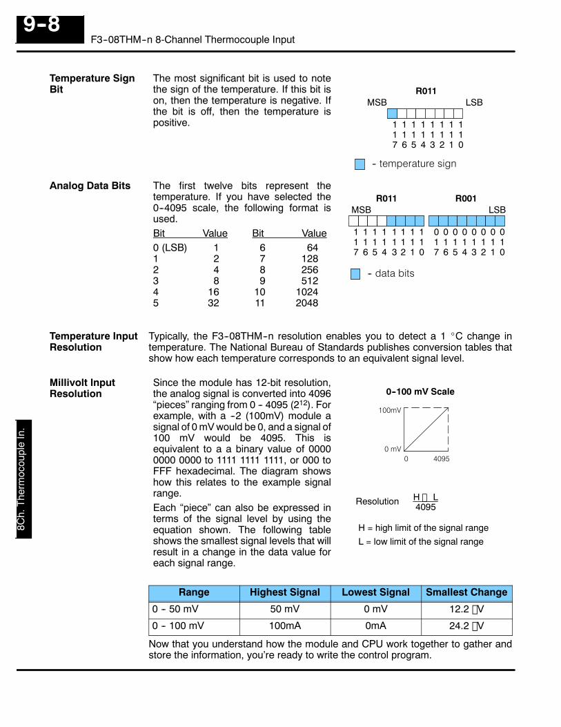
F3--0
8TH
M--n
8Ch.
Ther
moc
oupl
eIn
.9--8
F3--08THM--n 8-Channel Thermocouple Input
The most significant bit is used to notethe sign of the temperature. If this bit ison, then the temperature is negative. Ifthe bit is off, then the temperature ispositive.
R011MSB LSB
110
117
116
115
114
113
112
111
-- temperature sign
The first twelve bits represent thetemperature. If you have selected the0--4095 scale, the following format isused.Bit Value Bit Value0 (LSB) 1 6 641 2 7 1282 4 8 2563 8 9 5124 16 10 10245 32 11 2048
117
R001MSB LSB
010
116
115
114
113
112
111
110
017
016
015
014
013
012
011
-- data bits
R011
Typically, the F3--08THM--n resolution enables you to detect a 1 _C change intemperature. The National Bureau of Standards publishes conversion tables thatshow how each temperature corresponds to an equivalent signal level.
Since the module has 12-bit resolution,the analog signal is converted into 4096“pieces” ranging from 0 -- 4095 (212). Forexample, with a --2 (100mV) module asignal of 0 mV would be 0, and a signal of100 mV would be 4095. This isequivalent to a a binary value of 00000000 0000 to 1111 1111 1111, or 000 toFFF hexadecimal. The diagram showshow this relates to the example signalrange.Each “piece” can also be expressed interms of the signal level by using theequation shown. The following tableshows the smallest signal levels that willresult in a change in the data value foreach signal range.
100mV
0 mV0 4095
0--100 mV Scale
Resolution = H ≡ L4095
H = high limit of the signal rangeL = low limit of the signal range
Range Highest Signal Lowest Signal Smallest Change
0 -- 50 mV 50 mV 0 mV 12.2 µV
0 -- 100 mV 100mA 0mA 24.2 µV
Now that you understand how the module and CPU work together to gather andstore the information, you’re ready to write the control program.
Temperature SignBit
Analog Data Bits
Temperature InputResolution
Millivolt InputResolution

F3--08THM
--n8C
h.Thermocouple
In.9--9
F3--08THM--n 8-Channel Thermocouple Input
Writing the Control Program
Since all channels are multiplexed into a single data word, the control program mustbe setup to determine which channel is being read. Since the module provides inputpoints to the CPU, it is very easy to use the channel status bits to determine whichchannel is being monitored.
F3--08THM
R 011MSB LSB
R 001MSB LSB
010
R 002, R012 R 000, R010
8ptRelay
8ptOutput
16ptInput
16pt(Analog)
8chInput
8ptOutput
050--
057
040--
047
030--
037
020027
--120127
000007
--100107
010017
--110117
017
110
117
116
115
114
-- temperature sign
-- data bits
-- active channelindicator inputs
If you are using the temperature scale (°F or° C) then you do not have to perform anyscaling. Once you convert the binary temperature reading to a four-digit BCDnumber, you have the temperature.
Identifying theData Locations
AutomaticTemperatureConversion

F3--0
8TH
M--n
8Ch.
Ther
moc
oupl
eIn
.9--10
F3--08THM--n 8-Channel Thermocouple Input
The following example shows a program designed to read any of the availablechannels of data into Register locations. Once the data is in a Register, you canperform math on the data, compare the data against preset values, etc. Since theDL305 CPUs use 8-bit word instructions, you have to move the data in pieces. It’ssimple if you follow the example.
374DSTR3R011
F53
Read the data
This rung loads the four data bits into theaccumulator from Register 011 on every scan.
DOUT1R501
F61
114DOUTR400
F60
Store channel 1
DOUTR402
F60
Store channel 2
DOUTR404
F60
Store channel 3
The channel selection inputs are used to let theCPU know which channel has been loaded into theaccumulator. By using these inputs to control aDOUT instruction, you can easily move the data toa storage register. Notice the DOUT instructionstores the data in two bytes. (Two bytes arerequired for four digit BCD numbers.)
Temporarily store the bits to Register 501.
DSTR1R001
F51 This rung loads the eight data bits into theaccumulator from Register 001.
DOUT1R500
F61 Temporarily store the bits to Register 500. Sincethe most significant bits were loaded into 501, nowR500 and R501 contain all twelve bits in order.
DSTRR500
F50
BCD F86
Now that all the bits are stored, load all twelve bitsinto the accumulator.
Math operations are performed in BCD. Thisinstruction converts the binary data to BCD. (Youcan omit this step if your application does notrequire the conversion.)
115 116
114 115 116
114 115 116
114DOUTR406
F60
Store channel 4
DOUTR410
F60
Store channel 5
DOUTR412
F60
Store channel 6
115 116
114 115 116
114 115 116
DOUTR414
F60
Store channel 7
DOUTR416
F60
Store channel 8
114 115 116
114 115 116

F3--08THM
--n8C
h.Thermocouple
In.9--11
F3--08THM--n 8-Channel Thermocouple Input
By adding a couple of simple rungs you can easily monitor the temperature forpositive vs. negative readings. (For example, you have to know whether thetemperature is +100 _F or --100 _F.) Notice how we’ve changed Channel 2 to controlan output that denotes the sign of the temperature.
374DSTR3R011
F53
Read the data
This rung loads the four data bits into theaccumulator from Register 011 on every scan.
DOUT1R501
F61
114DOUTR400
F60
Store channel 1
DOUTR402
F60
Store channel 2
DOUTR404
F60
Store channel 3
The channel selection inputs are used to let theCPU know which channel has been loaded into theaccumulator. By using these inputs to control aDOUT instruction, you can easily move the data toa storage register. Notice the DOUT instructionstores the data in two bytes. (Two bytes arerequired for four digit BCD numbers.)
Temporarily store the bits to Register 501.
DSTR1R001
F51 This rung loads the eight data bits into theaccumulator from Register 001.
DOUT1R500
F61 Temporarily store the bits to Register 500. Sincethe most significant bits were loaded into 501, nowR500 and R501 contain all twelve bits in order.
DSTRR500
F50
BCD F86
Now that all the bits are stored, load all twelve bitsinto the accumulator.
Math operations are performed in BCD. Thisinstruction converts the binary data to BCD. (Youcan omit this step if your application does notrequire the conversion.)
115 116
114 115 116
114 115 116
114DOUTR406
F60
Store channel 4115 116
SET200114 115 116 117 If 117 is on, then the temperature on channel 2 is
negative.
RST200114 115 116 117 If 117 is off, then the temperature on channel 2 is
positive.
Using the Sign Bit

F3--0
8TH
M--n
8Ch.
Ther
moc
oupl
eIn
.9--12
F3--08THM--n 8-Channel Thermocouple Input
The example below shows how to read multiple channels on an F3--08THMThermocouple module in the X0 address of the D3--XX--1 Base.
_On
LDF
K12
X0 This loads the upper byte of the analog data fromthe module.
Load the data
SP1
BCD The BCD command converts the data to BCDformat.
OUTV1400
The scaled value is stored in V3010 with animplied decimal.
This writes channel one data to V2000when bits X14, X15 and X16 are asshown.
LD
V1400
Channel 1 Select Bit States
X15X14 X16
OUTV2000
This writes channel two data to V2002when bits X14, X15 and X16 are asshown.
LD
V1400
Channel 2 Select Bit States
X15X14 X16
OUTV2001
This writes channel three data toV2002 when bits X14, X15 and X16are as shown.
LD
V1400
Channel 3 Select Bit States
X15X14 X16
OUTV2002
This writes channel four data to V2003when bits X14, X15 and X16 are asshown.
LD
V1400
Channel 4 Select Bit States
X15X14 X16
OUTV2003
Reading MultipleChannels on aDL350 with aD3--XX--1 Base

F3--08THM
--n8C
h.Thermocouple
In.9--13
F3--08THM--n 8-Channel Thermocouple Input
This writes channel five data to V2004when bits X14, X15 and X16 are asshown.
LD
V1400
Channel 5 Select Bit States
X15X14 X16
OUTV2004
This writes channel six data to V2005when bits X14, X15 and X16 are asshown.
LD
V1400
Channel 6 Select Bit States
X15X14 X16
OUTV2005
This writes channel seven data toV2006 when bits X14, X15 and X16are as shown.
LD
V1400
Channel 7 Select Bit States
X15X14 X16
OUTV2006
This writes channel eight data toV2007 when bits X14, X15 and X16are as shown.
LD
V1400
Channel 8 Select Bit States
X15X14 X16
OUTV2007
SETC0X14 X15 X16 X17 When the sign bit is on, the sign control relay (C0)
is set, causing the temperature on channel one tobe negative.
RSTC0
When the sign bit is not true, the sign bit control bitis reset, causing the temperature on channel oneto be positive.
X14 X15 X16 X17
Channel 1 Selected
Using the Sign Bit
X17 is the sign bit when in module address 0.

F3--0
8TH
M--n
8Ch.
Ther
moc
oupl
eIn
.9--14
F3--08THM--n 8-Channel Thermocouple Input
If you are using the --1 (50mV) or the--2 (100mV) versions, you may want toscale the data to represent themeasurements in engineering units,which provide more meaningful data.This is accomplished by using theconversion formula shown.
NOTE: The thermocouple versionsautomatically provide the correcttemperature readings. Scaling is notrequired.
Units = A4096 S
Units = value in Engineering UnitsA = Analog value (0 -- 4095)S = high limit of the Engineering
unit range
The following example shows how youwould use the analog data to representpressure (PSI) from 0 to 100. Thisexample assumes the analog value is1760. This should yield approximately42.9 PSI.
Units = 17604096
100
Units = A4096 S
Units = 42.9
Scaling the InputData

F3--08THM
--n8C
h.Thermocouple
In.9--15
F3--08THM--n 8-Channel Thermocouple Input
The following instructions are required to scale the data. (We’ll continue to use the42.9 PSI example.) Once we’ve explained how these instructions operate, we’llshow an example program.
DSTRR400
F50
DIVK4096
F74
This instruction brings the analog value (in BCD)into the accumulator.
This instruction moves the two-byte decimalportion into the accumulator for further operations.
Scale the data
The analog value is divided by the resolution of themodule, which is 4096. (1760 / 4096 = 0.4296)
DSTRR576
F50
MULK100
F73
DSTRR576
F50
DOUTR450
F60
1 7 6 0Accumulator
0 0 0 0Aux. Accumulator
0 0 0 0Accumulator
4 2 9 6Aux. Accumulator
This example assumes you have already read the analog dataand stored the BCD equivalent in R400 and R401
4 2 9 6Accumulator
4 2 9 6Aux. Accumulator
The accumulator is then multiplied by the scalingfactor, which is 100. (100 x 4296 = 429600). Noticethe most significant digits are now stored in theauxilliary accumulator. (This is different from theway the Divide instruction operates.)
9 6 0 0Accumulator
0 0 4 2Aux. Accumulator
R577 R576
R577 R576
R577 R576
R577 R576
This instruction moves the two-byte auxilliaryaccumulator for further operations.
0 0 4 2Accumulator
0 0 4 2Aux. Accumulator
R577 R576
This instruction stores the accumulator to R450and R451. R450 and R451 now contain the PSI,which is 42 PSI.
0 0 4 2Accumulator
0 0 4 2Store in R451 & R450
R451 R450
114 115 116

F3--0
8TH
M--n
8Ch.
Ther
moc
oupl
eIn
.9--16
F3--08THM--n 8-Channel Thermocouple Input
You probably noticed the previous example yielded 42 PSI when the real valueshould have been 42.9 PSI. By changing the scaling value slightly, we can “imply” anextra decimal of precision. Notice in the following example we’ve added another digitto the scale. Instead of a scale of 100, we’re using 1000, which implies 100.0 for thePSI range.
DSTRR400
F50
DIVK4096
F74
This instruction brings the analog value (in BCD)into the accumulator.
This instruction moves the two-byte decimalportion into the accumulator for further operations.
Scale the data
The analog value is divided by the resolution of themodule, which is 4096. (1760 / 4096 = 0.4296)
DSTRR576
F50
MULK1000
F73
DSTRR576
F50
DOUTR450
F60
1 7 6 0Accumulator
0 0 0 0Aux. Accumulator
0 0 0 0Accumulator
4 2 9 6Aux. Accumulator
This example assumes you have already read the analog dataand stored the BCD equivalent in R400 and R401
4 2 9 6Accumulator
4 2 9 6Aux. Accumulator
The accumulator is multiplied by the scaling factor,which is now 1000. (1000 x 4296 = 4296000). Themost significant digits are now stored in theauxilliary accumulator. (This is different from theway the Divide instruction operates.)
6 0 0 0Accumulator
0 4 2 9Aux. Accumulator
R577 R576
R577 R576
R577 R576
R577 R576
This instruction moves the two-byte auxilliaryaccumulator for further operations.
0 4 2 9Accumulator
0 4 2 9Aux. Accumulator
R577 R576
This instruction stores the accumulator to R450and R451. R450 and R451 now contains the PSI,which implies 42.9.
0 4 2 9Accumulator
0 4 2 9Store in R451 & R450
R451 R450
114 115 116

F3--08THM
--n8C
h.Thermocouple
In.9--17
F3--08THM--n 8-Channel Thermocouple Input
This example program shows how you can use the instructions to load theseequation constants into data registers. The example is written for channel 1, but youcan easily use a similar approach to use different scales for all channels if required.You may just use the appropriate constants in the instructions dedicated for eachchannel, but this method allows easier modifications. For example, you could easilyuse an operator interface or a programming device to change the constants if theyare stored in Registers.
This rung loads the four most significant data bitsinto the accumulator from Register 011 on everyscan.
Temporarily store the bits to Register 501.
DSTR3R011
F53
DOUT1R501
F61
374Read the data
Store channel 1
374DSTRK4096
F50
DOUTR430
F60
DSTRK1000
F50
DOUTR432
F60
On the first scan, these first two instructions loadthe analog resolution (constant of 4096) into R430and R431.
These two instructions load the high limit of theEngineering unit scale (constant of 1000) intoR432 and R433. Note, if you have different scalesfor each channel, you’ll also have to enter theEngineering unit high limit for those as well.
Load the constants
DIVR430
F74
DSTRR576
F50
MULR432
F73
This instruction moves the decimal portion from theauxilliary accumulator into the regular accumulatorfor further operations.
The analog value is divided by the resolution of themodule, which is stored in R430 and R431.
DSTRR576
F50
DOUTR400
F60
The accumulator is multiplied by the scaling factor,which is stored in R432 and R433.
This instruction moves most significant digits (nowstored in the auxilliary accumulator) into theregular accumulator for further operations.
The scaled value is stored in R400 and R401 forfurther use.
114 115 116

F3--0
8TH
M--n
8Ch.
Ther
moc
oupl
eIn
.9--18
F3--08THM--n 8-Channel Thermocouple Input
Since the thermocouple devices are non-linear, it is much easier to rely on publishedstandards for conversion information. The National Bureau of Standards publishesconversion tables that show how each temperature corresponds to an equivalentsignal level.Sometimes it is helpful to be able to quickly convert between the signal levels and thedigital values. This is especially helpful during machine startup or troubleshooting.The following table provides formulas to make this conversion easier.
mV Range If you know the digital value ... If you know the analog signallevel ...
MV500 to 50 mV
MV1000 to 100 mV
For example, if you are using a--2 (100mV) version and you havemeasured the signal as 30 mV, youwould use the following formula todetermine the digital value that should bestored in the register location thatcontains the data.
D = 4095100
A
D = 4095100
(30)
D = (40.95) (30)
D = 1229
Now you have all the necessary information to get your analog module installed andoperating correctly!
Temperature andDigital ValueConversions
Millivolt and DigitalValue Conversions
A = 50D4095
D = 409550
A
A = 100D4095
D = 4095100
A

110F3--08TEMP8-ChannelTemperature Input
In This Chapter. . . .— Module Specifications— Setting the Module Jumpers— Connecting the Field Wiring— Module Operation— Writing the Control Program

F3--0
8TE
MP
8C
h.Te
mpe
ratu
reIn
put
10--2F3--08TEMP 8-Channel Temperature Input
Module Specifications
The F3--08TEMP Temperature Input Module provides eight, single-endedtemperature inputs for use with AD590 type temperature transmitters (range of0--1mA.) The module provides 12-bit resolution. You can use the RLL controlprogram to select between _F or _C operation.The following table provides the specifications for the F3--08TEMP TemperatureInput Module from FACTS Engineering. Review these specifications to make surethe module meets your application requirements.
Number of Channels 8, single-ended inputs
Input Ranges 0 -- 1 mA
Resolution 12 bit (1 in 4096)No missing codes 0.25 _C with AD590M
Input Impedance 10KO ? 0.1%
Absolute Maximum Ratings ? 50 mA
Conversion Time 35µs per channel, maximum1 channel per CPU scan
Converter Type Successive Approximation, AD574
Linearity Error ? 1 count (0.03% of full scale) maximum
Maximum Inaccuracy at 77 °F(25 °C)
0.25% of full scale
Accuracy at 25 _C ? 1 _C with AD590M transmitter
Accuracy vs. Temperature 57 ppm / _C maximum full scale
Power Budget Requirement 25 mA @ 9 VDC, 37 mA @ 24 VDC
External Power Supply None required
Operating Temperature 32° to 140° F (0° to 60° C)
Storage Temperature --4° to 158° F (--20° to 70° C)
Relative Humidity 5 to 95% (non-condensing)
Environmental air No corrosive gases permitted
Vibration MIL STD 810C 514.2
Shock MIL STD 810C 516.2
Noise Immunity NEMA ICS3--304

F3--08TEM
P8C
h.Temperature
Input10--3
F3--08TEMP 8-Channel Temperature Input
The following table provides the specifications for input temperature probescompatible with this module.
Compatible Temperature Probe Specifications
Transmitter Type AD590
Input Temperature Range --40° to 212° F (--40° to 100°C) --(Opto 22 PN ICTD)
--67° to 302° F (--55° to 150°C) --(Analog Devices PN AC2626J)
Transmitter Outputfor Opto 22 andAnalog Devices
1 µA / _K, 298.2 µA @ 25 _C218 µA @ --55 _C, 423 µA @ 150 _C
The F3--08TEMP Temperature Input appears as a 16-point module. The module canbe installed in any slot configured for 16 points. See the DL305 User Manual fordetails on using 16 point modules in DL305 systems. The limitation on the number ofanalog modules are:
S For local and expansion systems, the available power budget and16-point module usage are the limiting factors.
CompatibleTemperature ProbeSpecifications
Analog InputConfigurationRequirements

F3--0
8TE
MP
8C
h.Te
mpe
ratu
reIn
put
10--4F3--08TEMP 8-Channel Temperature Input
Setting the Module Jumpers
The module is set at the factory for eight-channel operation. If this is acceptable youdo not have to change any of the jumpers. The following diagram shows how thejumpers are set.
If you examine the rear of the module,you’ll notice several jumpers. Thejumpers labeled +1, +2 and +4 are usedto select the number of channels that willbe used. Without any jumpers themodule processes one channel. Byinstalling the jumpers you can addchannels. The module is set from thefactory for eight channel operation.For example, if you install the +1 jumper,you add one channel for a total of two.Now if you install the +2 jumper you addtwo more channels for a total of four.Any unused channels are not processedso if you only select channels 1--4, thenthe last four channels will not be active.The following table shows which jumpersto install.
Jumpers installed as shownselects 8-channel operation
+4 +2 +1
Number ofChannels
Channel(s) +4 +2 +11 No No No1 2 No No Yes1 2 3 No Yes No1 2 3 4 No Yes Yes1 2 3 4 5 Yes No No1 2 3 4 5 6 Yes No Yes1 2 3 4 5 6 7 Yes Yes No1 2 3 4 5 6 7 8 Yes Yes Yes
Factory Settings
Selecting theNumber ofChannels

F3--08TEM
P8C
h.Temperature
Input10--5
F3--08TEMP 8-Channel Temperature Input
Connecting the Field Wiring
Your company may have guidelines for wiring and cable installation. If so, you shouldcheck those before you begin the installation. Here are some general things toconsider.
S Use the shortest wiring route whenever possible.S Use shielded wiring and ground the shield at the signal source. Do not
ground the shield at both the module and the source.S Don’t run the signal wiring next to large motors, high current switches, or
transformers. This may cause noise problems.S Route the wiring through an approved cable housing to minimize the risk
of accidental damage. Check local and national codes to choose thecorrect method for your application.
The F3--08TEMP receives all power from the base. A separate power supply is notrequired.
The F3--08TEMP module has a removable connector to make wiring easier. Simplyremove the retaining screws and gently pull the connector from the module.
TEMP TRANSDUCERF3--08TEMP
COM
CH2
0V
CH1
0V
CH3
0VCH4
0V
COM
CH6
0V
CH5
0V
CH7
0VCH8
0V
CH2
IN
CH1
IN
CH3
INCH4
IN
CH6
IN
CH5
IN
CH7
INCH8
IN
COM
CH2
0V
CH1
0V
CH3
0VCH4
0V
COM
CH6
0V
CH5
0V
CH7
0VCH8
0V
CH2
IN
CH1
IN
CH3
INCH4
IN
CH6
IN
CH5
IN
CH7
INCH8
IN
N/C
N/C
N/C
N/C
N/C
N/C
N/C
N/C
+5 to+ --
AD590M
AD590M
AD590M
AD590M
AD590M
AD590M
AD590M
AD590M
AD590 TEMP TRANSDUCERPower Supply
0VIN
CH1
0VIN
CH2
0VIN
CH3
0VIN
CH4
0VIN
CH5
0VIN
CH6
0VIN
CH7
0VIN
CH8
10K
10K
10K
10K
10K
10K
10K
10K
COM
+30VDC
AD574
AnalogSwitch
Note 1: Terminate the shield at the signal source (0V reference potential)Note 2: Connect unused AD590 current inputs to 0VDC
See note
0V
COM
Wiring Guidelines
User Power SupplyRequirements
RemovableConnector
Wiring Diagram
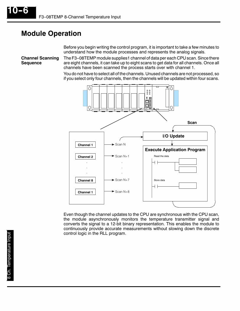
F3--0
8TE
MP
8C
h.Te
mpe
ratu
reIn
put
10--6F3--08TEMP 8-Channel Temperature Input
Module Operation
Before you begin writing the control program, it is important to take a few minutes tounderstand how the module processes and represents the analog signals.The F3--08TEMP module supplies1 channel of data per each CPU scan. Since thereare eight channels, it can take up to eight scans to get data for all channels. Once allchannels have been scanned the process starts over with channel 1.You do not have to select all of the channels. Unused channels are not processed, soif you select only four channels, then the channels will be updated within four scans.
Channel 1 Scan N
Read the data
Store data
I/O Update
Execute Application ProgramChannel 2 Scan N+1
Channel 8 Scan N+7
Channel 1 Scan N+8
Scan
.
.
.
.
.
.
Even though the channel updates to the CPU are synchronous with the CPU scan,the module asynchronously monitors the temperature transmitter signal andconverts the signal to a 12-bit binary representation. This enables the module tocontinuously provide accurate measurements without slowing down the discretecontrol logic in the RLL program.
Channel ScanningSequence

F3--08TEM
P8C
h.Temperature
Input10--7
F3--08TEMP 8-Channel Temperature Input
You may recall the F3--08TEMP module appears to the CPU as a 16-point module.These 16 points provide:
S an indication of which channel is active.S the digital representation of the temperature.
Since all I/O points are automatically mapped into Register (R) memory, it is veryeasy to determine the location of the data word that will be assigned to the module.
110
F3--08TEMP
R 011MSB LSB
R 001MSB LSB
010
R 002, R012 R 000, R010
117
8ptRelay
8ptOutput
16ptInput
16pt(Analog)
8chInput
8ptOutput
050--
057
040--
047
030--
037
020027
--120127
000007
--100107
010017
--110117
017
-- not used
Within these two register locations, the individual bits represent specific informationabout the analog signal.
The next to last three bits of the upperRegister indicate the active channel. Theindicators automatically increment witheach CPU scan.
Active ChannelScan Inputs ChannelN 000 1N+1 001 2N+2 010 3N+3 011 4N+4 100 5N+5 101 6N+6 110 7N+7 111 8N+8 000 1
R011MSB LSB
110
117
116
115
114
113
112
111
-- active channelindicator inputs
Understanding theI/O Assignments
Active ChannelIndicator Inputs

F3--0
8TE
MP
8C
h.Te
mpe
ratu
reIn
put
10--8F3--08TEMP 8-Channel Temperature Input
The first twelve bits represent thetemperature. The following format isused.Bit Value Bit Value0 (LSB) 1 6 641 2 7 1282 4 8 2563 8 9 5124 16 10 10245 32 11 2048
117
R001MSB LSB
010
116
115
114
113
112
111
110
017
016
015
014
013
012
011
-- data bits
R011
Typically, the F3--08TEMP resolution enables you to detect a 0.1 _F change intemperature.Now that you understand how the module and CPU work together to gather andstore the information, you’re ready to write the control program.
Analog Data Bits
Temperature InputResolution

F3--08TEM
P8C
h.Temperature
Input10--9
F3--08TEMP 8-Channel Temperature Input
Writing the Control Program
Since all channels are multiplexed into a single data word, the control program mustbe setup to determine which channel is being read. Since the module provides inputpoints to the CPU, it is very easy to use the channel status bits to determine whichchannel is being monitored.
110
F3--08TEMP
R 011MSB LSB
R 001MSB LSB
010
R 002, R012 R 000, R010
117
8ptRelay
8ptOutput
16ptInput
16pt(Analog)
8chInput
8ptOutput
050--
057
040--
047
030--
037
020027
--120127
000007
--100107
010017
--110117
017
-- not used
The following example program is designed to read any of the available channels ofdata . Once the data is read, you’ll have to add some logic to convert the data into a_C or _F temperature. (More on the conversion in a minute. For now, let’s just readthe value into the accumulator.) Since the DL305 CPUs use 8-bit word instructions,you have to move the data in pieces. It’s simple if you follow the example.
374DSTR3R011
F53
Read the data
This rung loads the four data bits into theaccumulator from Register 011 on every scan.
DOUT1R501
F61 Temporarily store the bits to Register 501.
DSTR1R001
F51 This rung loads the eight data bits into theaccumulator from Register 001.
DOUT1R500
F61 Temporarily store the bits to Register 500. Sincethe most significant bits were loaded into 501, nowR500 and R501 contain all twelve bits in order.
DSTRR500
F50
BCD F86
Now that all the bits are stored, load all twelve bitsinto the accumulator.
Math operations are performed in BCD. Thisinstruction converts the binary data to BCD. (We’llhave to use math to convert the value to atemperature.)
Identifying theData Locations
Reading the DigitalValue

F3--0
8TE
MP
8C
h.Te
mpe
ratu
reIn
put
10--10F3--08TEMP 8-Channel Temperature Input
Once the input data is stored in a register location, you will need to convert it torepresent the temperature you are measuring. Use the formulas shown to convertthe data to show the temperature in _C and _F.
Temp = 1000 A4096 ≡ 273.2
Temp = temperature in _CA = Analog value (0 -- 4095)273.2 = _K offset(0 _K = --273.2 _C)
For _C Readings
Temp = 1000 A2276 ≡ 459.6
Temp = temperature in _FA = Analog value (0 -- 4095)459.6 = _K offset(0 _K = --459.6 _F)
For _F Readings
Temp = 1000 17334096
≡ 273.2The following example shows how youwould use the analog data to representthe temperature. This example assumesthe analog value is 1733. This shouldyield approximately 150 _C.
Temp = 149.9
You can’t quite enter the formula exactly as is with the DL305 instruction set. Youhave to use a value that implies the decimal point of precision. Plus, since we canmove the decimal portion into the accumulator, we do not have to multiply the valueby 1000.The following instructions show you how to solve the conversion problem. (We’llcontinue to use the 150 _C example.)
Converting theData toTemperature

F3--08TEM
P8C
h.Temperature
Input10--11
F3--08TEMP 8-Channel Temperature Input
NOTE: This example uses °C. To use °F, simply change the scaling factor and offsetinstructions to use the F formula.
S _F scale — Constant of 2276 for scaling factor, constant of 4596 foroffset.
S _C scale — constant of 4096 for scaling factor, constant of 2732 foroffset.
DIVK4096
F74
This instruction moves the two-byte decimalportion into the accumulator for further operations.
Scale the data
The analog value is divided by _C scaling factor,which is 4096. (1733 / 4096 = 0.4230)
DSTRR576
F50
SUBK2732
F72
1 7 3 3Accumulator
0 0 0 0Aux. Accumulator
0 0 0 0Accumulator
4 2 3 0Aux. Accumulator
4 2 3 0Accumulator
4 2 3 0Aux. Accumulator
Now subtract the _K offset from the accumulator.(The _K offset is 2732, which represents 273.2 _.
4 2 3 0Accumulator
2 7 3 2Constant
R577 R576
R577 R576
R577 R576
--1 4 9 8
Accumulator
DSTR3R011
F53
Read the data
This rung loads the four data bits into theaccumulator from Register 011 on ever scan.
DOUT1R501
F61 Temporarily store the bits to Register 501.
DSTR1R001
F51 This rung loads the eight data bits into theaccumulator from Register 001.
DOUT1R500
F61 Temporarily store the bits to Register 500. Sincethe most significant bits were loaded into 501, nowR500 and R501 contain all twelve bits in order.
DSTRR500
F50
BCD F86
Now that all the bits are stored, load all twelve bitsinto the accumulator.
Math operations are performed in BCD. Thisinstruction converts the binary data to BCD. (We’llhave to use math to convert the value to atemperature.)
374
374

F3--0
8TE
MP
8C
h.Te
mpe
ratu
reIn
put
10--12F3--08TEMP 8-Channel Temperature Input
Temp = 1000 9964096
≡ 273.2You have to perform some additionalcalculations if the temperature is belowzero. Since the DL305 sets a specialcontact 775 if the subtraction results in avalue below zero, you can use this toindicate further calculations are required.The following example shows the scalingand zero indication for a temperature of--30 C.
Temp = ≡ 30.0
374
374DIVK4096
F74
This instruction moves the two-byte decimalportion into the accumulator for further operations.
Scale the data
The analog value is divided by _C scaling factor,which is 4096. (996 / 4096 = 0.2431)
DSTRR576
F50
SUBK2732
F72
0 9 9 6Accumulator
0 0 0 0Accumulator
2 4 3 1Aux. Accumulator
2 4 3 1Accumulator
2 4 3 1Aux. Accumulator
Now subtract the _K offset from the accumulator.(The _K offset is 2732, which represents 273.2 _.
2 4 3 1Accumulator
2 7 3 2Constant
R577 R576
R577 R576
--0 6 9 9
Accumulator
This example assumes you have already read the analog datainto the accumulator and converted the data to BCD.
SP7751 (on)
DOUTR500
F60
Store 0000 in the accumulator. This will allow us tocalculate the correct value.
Below zero correction
If 775 is on, the value is temporarily stored inregisters (R500 and R501 in this case).
DSTRK0000
F50
SUBR500
F72
0 6 9 9Accumulator
0 6 9 9
0 0 0 0Accumulator
Now subtract the original answer (which was0699.) 0 -- 0699 = 0301, or 30.1 _C
0 0 0 0Accumulator
0 6 9 9Constant
R501 R500
--0 3 0 1
Accumulator SP7751 (on)
775
Since the DL305 encountered a negative number, itturns contact 775 on to indicate a borrow.
ReadingTemperaturesBelow Zero

F3--08TEM
P8C
h.Temperature
Input10--13
F3--08TEMP 8-Channel Temperature Input
Once you’ve read the data and converted it to a temperature, you can use thechannel selection inputs to store each of the eight channels. Once you’ve stored thedata you can perform data comparisons, additional math, etc.
DIVK4096
F74
This instruction moves the two-byte decimalportion into the accumulator for further operations.
Scale the data
The analog value is divided by _C scaling factor,which is 4096. (1733 / 4096 = 0.4230)
DSTRR576
F50
SUBK2732
F72Now subtract the _K offset from the accumulator.(The _K offset is 2732, which represents 273.2 _.
DSTR3R011
F53
Read the data
This rung loads the four data bits into theaccumulator from Register 011.
DOUT1R501
F61 Temporarily store the bits to Register 501.
DSTR1R001
F51 This rung loads the eight data bits into theaccumulator from Register 001.
DOUT1R500
F61 Temporarily store the bits to Register 500. Sincethe most significant bits were loaded into 501, nowR500 and R501 contain all twelve bits in order.
DSTRR500
F50
BCD F86
Now that all the bits are stored, load all twelve bitsinto the accumulator.
Math operations are performed in BCD. Thisinstruction converts the binary data to BCD. (We’llhave to use math to convert the value to atemperature.)
DOUTR500
F60
Store 0000 in the accumulator. This will allow us tocalculate the correct value.
Below zero correction
If 775 is on, the value is temporarily stored inregisters (R500 and R501 in this case).
DSTRK0000
F50
SUBR500
F72Now subtract the original answer (which was0699.) 0 -- 0699 = 0301, or 30.1 _C
775
114DOUTR400
F60
Store channel 1
DOUTR402
F60
Store channel 2
115 116
114 115 116
DOUTR416
F60
Store channel 8114 115 116
Use the channel selection bits to determine whichchannel is active. For example, this rung storeschannel 1 temperature in registers 400 and 401.
374
374
374
Storing theTemperature

F3--0
8TE
MP
8C
h.Te
mpe
ratu
reIn
put
10--14F3--08TEMP 8-Channel Temperature Input
The example below shows how to read an Analog Devices AD590 temperaturetransducer on an F3--08TEMP Temperature Input module in the X0 address of theD3--XX--1 Base.
_FirstScan
LD
K2732This loads the offset for Celcus conversion, whichis 273.2 degrees.
SP0
OUT This stores the offset in V1401.V1401
LD
K4096This loads the scaling factor, 4096.
OUT This stores the scaling factor in V1402.V1402
_On
LDF
K12This loads the first twelve bits.
SP1
BCD This converts to BCD.
DIV
V1402This scales the value for Celsius.
SHFL This shifts the BCD value 16 bits to the left. This isthe equivalent of multiplying by 1000.K16
X0
SUB This subtracts the offset for Celsius.V1401
_On
OUT
V1400This stores the 12 Bit Analog Data in V1400.
SP1
LD Loads a Zero into the accumulator.
DIV
V1402This scales the value for Celsius.
SUB Subtracts the value in V1400 from zero, resultingin a negative number.V1400
Sets control relay C0.
SP64
Convert fromKelvin to Celsius
Check for “Borrow” or Negative
K0
SETC0
ReadingTemperatures on aDL350 with aD3--XX--1 Base

F3--08TEM
P8C
h.Temperature
Input10--15
F3--08TEMP 8-Channel Temperature Input
This writes channel one data to V2000when bits X14, X15 and X16 are asshown.
Channel 1 Select Bit States
X15X14 X16OUT
V2000
SETC1
When the appropriate channel select bits are turned on, theconverted analog data is then stored in V-memory locations,starting with V2000 (for channel 1).
X14C0 X15 X16
RSTC1X14C0 X15 X16
These two rungs control the negative indicator bit.When the channels select bits are true for aparticular channel and C0 is on, the negative bitfor that channel is set. When the temperature goesabove 0 Celsius, the bit is reset.
Notice that this only applies to Channels 1.
The negative indicator bit
This writes channel two data to V2001when bits X14, X15 and X16 are asshown.
Channel 2 Select Bit States
X15X14 X16OUT
V2001
The remaining channels are shown below, without covering the negative bit logic.
This writes channel three data toV2002 when bits X14, X15 and X16are as shown.
Channel 3 Select Bit States
X15X14 X16OUT
V2002

F3--0
8TE
MP
8C
h.Te
mpe
ratu
reIn
put
10--16F3--08TEMP 8-Channel Temperature Input
OUT
V3003
Channel 4 Select Bit States
OUT
V3004
Channel 5 Select Bit States
OUT
V3005
Channel 6 Select Bit States
OUT
V3006
Channel 7 Select Bit States
X125X124 X126
X125X124 X126
X125X124 X126
X125X124 X126
OUT
V3007
Channel 8 Select Bit StatesX125X124 X126
This writes channel four analog data to V3003when bits X124, X125 and X126 are as shown.
This writes channel five analog data to V3004when bits X124, X125 and X126 are as shown.
This writes channel six analog data to V3005 whenbits X124, X125 and X126 are as shown.
This writes channel seven analog data to V3006when bits X124, X125 and X126 are as shown.
This writes channel eight analog data to V3007when bits X124, X125 and X126 are as shown.

F3--08TEM
P8C
h.Temperature
Input10--17
F3--08TEMP 8-Channel Temperature Input
Sometimes it is helpful to be able to quickly convert between the signal levels and thedigital values. This is especially helpful during machine startup or troubleshooting.The following table provides formulas to make this conversion easier.
Range If you know the digital value ... If you know the temperature ...
--55 to150 _C
--67 to 302 _F
For example, if you have measured thetemperature at 30 _C, you would use thefollowing formula to determine the digitalvalue that should be stored in the registerlocation that contains the temperature.
D = 40951000
(T + 273.2)
D = 40951000
(30 + 273.2)
D = (4.095) (303.2)
D = 1241
Now you have all the necessary information to get your analog module installed andoperating correctly!
Temperature andDigital ValueConversions
T = 1000D4095 ≡ 273.2 D = 4095
1000(T + 273.2)
T = 1000D2276 ≡ 459.6 D = 2276
1000(T + 459.6)

1ADL305Data Types andMemory Map
In This Chapter. . . .— DL330 Memory Map— DL330P Memory Map— DL340 Memory Map— I/O Point Bit Map— Control Relay Bit Map— Special Relays— Data Registers

App
endi
xA
Dat
aTy
pes
&M
em.M
apA
ppen
dix
ED
L305
Mem
ory
Map
A--2DL305 Data Types and Memory Map
DL330 Memory MapMemory Type Discrete Memory
Reference(octal)
Register MemoryReference
(octal)
Qty.Decimal
Symbol
Input / OutputPoints
000 -- 157700 -- 767
R000 -- R015R070 -- R076
168 Total
Control Relays 160 -- 373 R016 -- R037 140
Special Relays 374 -- 377770 -- 777
R037R077
12
Timers /Counters
600 -- 673674 -- 677*
None 64
Timer / CounterCurrent Values
None R600 -- R673R674 -- R677*
64
Timer / CounterStatus Bits
T600 -- T673T674 -- T677*
None 64
Data Words None R400 -- R563 116 None specific, used with manyinstructions
Shift Registers 400 -- 577 None 128
SpecialRegisters
None R574 -- R577 4 R574 -- R575 used with FAULTR576 -- R577 Auxiliary Accumulator
* T/ C Setpoint Unit Only. Can be used as data registers if the Timer/Counter Setpoint Unit or Thumbwheel Interface Module is not used. R564 -- R573 contain the preset value used with the Timer /
Counter Setpoint Unit. R674 -- R677 contain the current values for these timers or counters.
000 010
C0C0
772 376
TMR T600K100
CNT C600K10
R600 K100
T600
SR400417

Appendix
AD
ataTypes
&M
em.M
apA
ppendixE
DL305
Mem
oryM
apA--3
DL305 Data Types and Memory Map
DL330P Memory MapMemory Type Discrete Memory
Reference(octal)
Register MemoryReference
(octal)
Qty.Decimal
Symbol
Input / OutputPoints
000 -- 157700 -- 767
R000 -- R015R070 -- R076
168 Total
Control Relays 160 -- 174200 -- 277
R016 -- R017R020 -- R027
77
Special Relays 175 -- 177770 -- 777
R017R077
11
Timers /Counters
600 -- 673674 -- 677*
None 64
Timer / CounterCurrent Values
None R600 -- R673R674 -- R677*
64
Timer / CounterStatus Bits
T600 -- T673T674 -- T677*
None 64
Data Words None R400 -- R563 116 None specific, used with manyinstructions
Stages S0 -- S177 R100 -- R117 128
SpecialRegisters
None R574 -- R577 4 R574 -- R575 used with FAULTR576 -- R577 Auxiliary Accumulator
* T/ C Setpoint Unit Only. Can be used as data registers if the Timer/Counter Setpoint Unit or Thumbwheel Interface Module is not used, which provides a total of 128 data registers.
R564 -- R573 contain the preset value used with the Timer / Counter Setpoint Unit. R674 -- R677 contain the current values for these timers or counters.
000 010
C0C0
772 176
TMR T600K100
CNT C600K10
R600 K100
T600
SGS 001
S1

App
endi
xA
Dat
aTy
pes
&M
em.M
apA
ppen
dix
ED
L305
Mem
ory
Map
A--4DL305 Data Types and Memory Map
DL340 Memory MapMemory Type Discrete Memory
Reference(octal)
Register MemoryReference
(octal)
Qty.Decimal
Symbol
Input / OutputPoints
000 -- 157700 -- 767
R000 -- R015R070 -- R076
168 Total
Control Relays 160 -- 3731000 -- 1067
R016 -- R037R100 -- R106
180
Special Relays 374 -- 377770 -- 7771070 -- 1077
R037R077R107
20
Timers /Counters
600 -- 673674 -- 677*
None 64
Timer / CounterCurrent Values
None R600 -- R673R674 -- R677*
64
Timer / CounterStatus Bits
T600 -- T673T674 -- T677*
None 64
Data Words None R400 -- R563R700 -- R767
172 None specific, used with manyinstructions
Shift Registers 400 -- 577 None 128
SpecialRegisters
None R574 -- R577R770 -- R777
12 R574--R575 used with FAULTR576--R577 Auxiliary AccumulatorR770--R777 Communications Setup
* T/ C Setpoint Unit Only. Can be used as data registers if the Timer/Counter Setpoint Unit or Thumbwheel Interface Module is not used. R564 -- R573 contain the preset value used with the Timer /
Counter Setpoint Unit. R674 -- R677 contain the current values for these timers or counters.
000 010
C0C0
772 376
TMR T600K100
CNT C600K10
R600 K100
T600
SR400417

Appendix
AD
ataTypes
&M
em.M
apA
ppendixE
DL305
Mem
oryM
apA--5
DL305 Data Types and Memory Map
I/O Point Bit Map
These tables provide a listing of the individual Input points associated with eachregister location for the DL330, DL330P, and DL340 CPUs.
MSB I/O References LSB RegisterNumber
007 006 005 004 003 002 001 000 R0017 016 015 014 013 012 011 010 R1027 026 025 024 023 022 021 020 R2037 036 035 034 033 032 031 030 R3047 046 045 044 043 042 041 040 R4057 056 055 054 053 052 051 050 R5067 066 065 064 063 062 061 060 R6077 076 075 074 073 072 071 070 R7107 106 105 104 103 102 101 100 R10117 116 115 114 113 112 111 110 R11127 126 125 124 123 122 121 120 R12137 136 135 134 133 132 131 130 R13147 146 145 144 143 142 141 140 R14157 156 155 154 153 152 151 150 R15167 166 165 164 163 162 161 160 n/a177 176 175 174 173 172 171 170 n/a707 706 705 704 703 702 701 700 R70717 716 715 714 713 712 711 710 R71727 726 725 724 723 722 721 720 R72737 736 735 734 733 732 731 730 R73747 746 745 744 743 742 741 740 R74757 756 755 754 753 752 751 750 R75767 766 765 764 763 762 761 760 R76
NOTE: 160 -- 167 can be used as I/O in a DL330 or DL330P CPU under certainconditions. 160 -- 177 can be used as I/O in a DL340 CPU under certain conditions.You should consult the DL305 User Manual to determine which configurations allowthe use of these points.
These points are normally used as control relays. You cannot use them as bothcontrol relays and as I/O points. Also, if you use these points as I/O, you cannotaccess these I/O points as a Data Register reference.

App
endi
xA
Dat
aTy
pes
&M
em.M
apA
ppen
dix
ED
L305
Mem
ory
Map
A--6DL305 Data Types and Memory Map
Control Relay Bit Map
The following tables provide a listing of the individual control relays associated witheach register location for the DL305 CPUs.
NOTE: 160 -- 167 can be used as I/O in a DL330 or DL330P CPU under certainconditions. 160 -- 177 can be used as I/O in a DL340 CPU under certain conditions.You should consult the DL305 User Manual to determine which configurations allowthe use of these points.
You cannot use them as both control relays and as I/O points. Also, if you use thesepoints as I/O, you cannot access these I/O points as a Data Register reference.
MSB DL330Control Relay References
LSB RegisterNumber
167 166 165 164 163 162 161 160 R16177 176 175 174 173 172 171 170 R17207 206 205 204 203 202 201 200 R20217 216 215 214 213 212 211 210 R21227 226 225 224 223 222 221 220 R22237 236 235 234 233 232 231 230 R23247 246 245 244 243 242 241 240 R24257 256 255 254 253 252 251 250 R25267 266 265 264 263 262 261 260 R26277 276 275 274 273 272 271 270 R27307 306 305 304 303 302 301 300 R30317 316 315 314 313 312 311 310 R31327 326 325 324 323 322 321 320 R32337 336 335 334 333 332 331 330 R33347 346 345 344 343 342 341 340 R34357 356 355 354 353 352 351 350 R35367 366 365 364 363 362 361 360 R36
373 372 371 370 R37
* Control relays 340 -- 373 can be made retentive by setting a CPU dipswitch. See the DL305 User Manual for detailson setting CPU dipswitches.

Appendix
AD
ataTypes
&M
em.M
apA
ppendixE
DL305
Mem
oryM
apA--7
DL305 Data Types and Memory Map
MSB DL330PControl Relay References
LSB RegisterNumber
167 166 165 164 163 162 161 160 R16174 173 172 171 170 R17
207 206 205 204 203 202 201 200* R20217 216 215 214 213 212 211 210 R21227 226 225 224 223 222 221 220 R22237 236 235 234 233 232 231 230 R23247 246 245 244 243 242 241 240 R24257 256 255 254 253 252 251 250 R25267 266 265 264 263 262 261 260 R26277* 276 275 274 273 272 271 270 R27
* Control relays 200 -- 277 can be made retentive by setting a CPU dipswitch. See the DL305 User Manual for details on setting CPU dipswitches.
MSB DL340Control Relay References
LSB RegisterNumber
167 166 165 164 163 162 161 160 R16177 176 175 174 173 172 171 170 R17207 206 205 204 203 202 201 200 R20217 216 215 214 213 212 211 210 R21227 226 225 224 223 222 221 220 R22237 236 235 234 233 232 231 230 R23247 246 245 244 243 242 241 240 R24257 256 255 254 253 252 251 250 R25267 266 265 264 263 262 261 260 R26277 276 275 274 273 272 271 270 R27307 306 305 304 303 302 301 300 R30317 316 315 314 313 312 311 310 R31327 326 325 324 323 322 321 320 R32337 336 335 334 333 332 331 330 R33347 346 345 344 343 342 341 340* R34357 356 355 354 353 352 351 350 R35367 366 365 364 363 362 361 360 R36
373* 372 371 370 R371007 1006 1005 1004 1003 1002 1001 1000 R1001017 1016 1015 1014 1013 1012 1011 1010 R1011027 1026 1025 1024 1023 1022 1021 1020 R1021037 1036 1035 1034 1033 1032 1031 1030 R1031047 1046 1045 1044 1043 1042 1041 1040 R1041057 1056 1055 1054 1053 1052 1051 1050 R1051067 1066 1065 1064 1063 1062 1061 1060 R106
* Control relays 340 -- 373 can be made retentive by setting a CPU dipswitch. See the DL305 User Manual for detailson setting CPU dipswitches.

App
endi
xA
Dat
aTy
pes
&M
em.M
apA
ppen
dix
ED
L305
Mem
ory
Map
A--8DL305 Data Types and Memory Map
Special Relays
The following table shows the Special Relays used with the DL305 CPUs.
CPUs SpecialRelay
Description of Contents
175 100 ms clock, on for 50 ms and off for 50 ms.
DL330P176 Disables all outputs except for those entered with the SET
OUT instruction.
177 Battery voltage is low.
374 On for the first scan cycle after the CPU is switched to RunMode.
DL330DL340
375 100 ms clock, on for 50 ms and off for 50 ms.DL330DL340 376 Disables all outputs except for those entered with the SET
OUT instruction.
377 Battery voltage is low.
770 Changes timers to 0.01 second intervals. Timers arenormally 0.1 second time intervals.
771 The external diagnostics FAULT instruction (F20) is in use.
DL330
772 The data in the accumulator is greater than the comparisonvalue.
DL330DL330PDL340
773 The data in the accumulator is equal to the comparisonvalue.
DL340774 The data in the accumulator is less than the comparison
value.
775 An accumulator carry or borrow condition has occurred.
776 The accumulator value is zero.
777 The accumulator has an overflow condition.
1074 The RX or WX instruction is active.
DL340
1075 An error occurred during communications with the RX orWX instructions.
DL340 1076 Port 2 communications mode: on = ASCII mode, off = HEXmode
1077 Port 1 communications mode: on = ASCII mode, off = HEXmode

Appendix
AD
ataTypes
&M
em.M
apA
ppendixE
DL305
Mem
oryM
apA--9
DL305 Data Types and Memory Map
Data Registers
The following 8-bit data registers are primarily used with data instructions to storevarious types of application data. For example, you could use a register to hold atimer or counter preset value.Some data instructions call for two bytes, which will correspond to two consecutive8-bit data registers such as R401 and R400. The LSB (Least Significant Bit) will be inregister R400 as bit0 and the MSB (Most Significant Bit) will be in register R401 asbit17.
NOTE: Data Registers are retentive.
DL330 / DL330P8-Bit Data Registers
407 406 405 404 403 402 401 400417 416 415 414 413 412 411 410427 426 425 424 423 422 421 420437 436 435 434 433 432 431 430447 446 445 444 443 442 441 440457 456 455 454 453 452 451 450467 466 465 464 463 462 461 460477 476 475 474 473 472 471 470507 506 505 504 503 502 501 500517 516 515 514 513 512 511 510527 526 525 524 523 522 521 520537 536 535 534 533 532 531 530547 546 545 544 543 542 541 540557 556 555 554 553 552 551 550
563 562 561 560

App
endi
xA
Dat
aTy
pes
&M
em.M
apA
ppen
dix
ED
L305
Mem
ory
Map
A--10DL305 Data Types and Memory Map
DL3408-Bit Data Registers
407 406 405 404 403 402 401 400417 416 415 414 413 412 411 410427 426 425 424 423 422 421 420437 436 435 434 433 432 431 430447 446 445 444 443 442 441 440457 456 455 454 453 452 451 450467 466 465 464 463 462 461 460477 476 475 474 473 472 471 470507 506 505 504 503 502 501 500517 516 515 514 513 512 511 510527 526 525 524 523 522 521 520537 536 535 534 533 532 531 530547 546 545 544 543 542 541 540557 556 555 554 553 552 551 550
563 562 561 560707 706 705 704 703 702 701 700717 716 715 714 713 712 711 710727 726 725 724 723 722 721 720737 736 735 734 733 732 731 730747 746 745 744 743 742 741 740757 756 755 754 753 752 751 750767 766 765 764 763 762 761 760

Appendix
AD
ataTypes
&M
em.M
apA
ppendixE
DL305
Mem
oryM
apA--11
DL305 Data Types and Memory Map
DL350 System V-memorySystem
V-memoryDescription of Contents Default Values / Ranges
V7620--V7627V7620V7621V7622V7623V7624V7625V7626V7627
Locations for DV--1000 operator interface parametersSets the V-memory location that contains the value.Sets the V-memory location that contains the message.Sets the total number (1 -- 16) of V-memory locations to be displayed.Sets the V-memory location that contains the numbers to be displayed.Sets the V-memory location that contains the character code to be displayed.Contains the function number that can be assigned to each key.ReservedReserved
V0 -- V3777V0 -- V37771 -- 16V0 -- V3777V0 -- V3777V-memory for X, Y, or C0,1,2,3,12Default=0000
V7630--V7632 Reserved --
V7633 User defined timer interrupt/operation of battery/Binary instruction sign flag*Bit 0--7 40H Setting InterruptBit 12 ON with battery sign flag. ON use sign flag --
OFF no sign flagBit 15 Binary instruction sign flag. ON use sign flag --
OFF no sign flag
V7634 User defined timer interrupt
V7640 Loop Table Beginning address V1400--V7340
V7641 Number of Loops Enabled 1--4
V7642 Error Code -- V--memory Error Location for Loop Table
V7643--V7647 Reserved
V7650 Port 2 End--code setting Setting (A55A), Nonprocedure communications start.
V7651 Port 2 Data format --Non--procedure communications format setting.
V7652 Port 2 Format Type setting -- Non--procedure communications type codesetting.
V7653 Port 2 Terminate--code setting -- Non--procedure communications Terminationcode setting.
V7654 Port 2 Store V--mem address -- Non--procedure communication data storeV--Memory address.
V7655 Port 2 Setup area --0--7 Comm protocol (flag 0) 8--15 Comm timeout/response delay time (flag 1)
V7656 Port 2 setup area -- 0--15 Communication (flag2, flag 3)
V7657 Port 2 setup area -- Bit to select use of parameter
V7660--V7707 Set--up Information
V7710--V7717 Reserved
V7720--V7722 Locations for DV--1000 operator interface parameters.V7720--V7722V7720V7721
Titled Timer preset value pointerV7720V7721V7722
Title Counter preset value pointerV7722 HiByte-Titled Timer preset block size, LoByte-Titled Counter preset block size
V7730--V7737 For slot 0 to 7 D3--DCM
V7747 Location contains a 10ms counter. This location increments once every 10ms.
V7750 Reserved

App
endi
xA
Dat
aTy
pes
&M
em.M
apA
ppen
dix
ED
L305
Mem
ory
Map
A--12DL305 Data Types and Memory Map
SystemV-memory
Description of Contents
V7751 Fault Message Error Code — stores the 4-digit code used with the FAULT instruction when theinstruction is executed.
V7752 Reserved
V7753 Reserved
V7754 Reserved
V7755 Error code — stores the fatal error code.
V7756 Error code — stores the major error code.
V7757 Error code — stores the minor error code.
V7760--V7762 Reserved
V7763--V7764 Location for syntax error information.
V7765 Scan — stores the total number of scan cycles that have occurred since the last Program Mode to RunMode transition.
V7766 Contains the number of seconds on the clock. (00 to 59).
V7767 Contains the number of minutes on the clock. (00 to 59).
V7770 Contains the number of hours on the clock. (00 to 23).
V7771 Contains the day of the week. (Mon, Tue, etc.).
V7772 Contains the day of the month (1st, 2nd, etc.).
V7773 Contains the month. (01 to 12)
V7774 Contains the year. (00 to 99)
V7775 Scan — stores the current scan time (milliseconds).
V7776 Scan — stores the minimum scan time that has occurred since the last Program Mode to Run Modetransition (milliseconds).
V7777 Scan — stores the maximum scan time that has occurred since the last Program Mode to Run Modetransition (milliseconds).
DL350 Comm Port 2 Control RelaysThe following system control relays are valid only for D3--350 CPU remote I/O setupon Communications Port 2.
System CRs Description of Contents
C740 Completion of setups -- ladder logic must turn this relay on when it has finished writing tothe Remote I/O setup table
C741 Erase received data -- turning on this flag will erase the received data during a communica-tion error.
C743 Re-start -- Turning on this relay will resume after a communications hang-up on an error.
C750 to C757 Setup Error -- The corresponding relay will be ON if the setup table contains an error (C750= master, C751 = slave 1... C757=slave 7
C760 to C767 Communications Ready -- The corresponding relay will be ON if the setup table data is valid(C760 = master, C761 = slave 1... C767=slave 7

Appendix
AD
ataTypes
&M
em.M
apA
ppendixE
DL305
Mem
oryM
apA--13
DL305 Data Types and Memory Map
DL350 Memory MapMemory Type Discrete Memory
Reference(octal)
Word MemoryReference
(octal)
Qty.Decimal
Symbol
Input Points X0 -- X777 V40400 -- V40437 512
Output Points Y0 -- Y777 V40500 -- V40537 512
Control Relays C0 -- C1777 V40600 -- V40677 1024
Special Relays SP0 -- SP777 V41200 -- V41237 512
Timer CurrentValues
None V0 -- V377 256
Timer Status Bits T0 -- T377 V41100 -- V41117 256
CounterCurrent Values
None V1000 -- V1177 128
Counter StatusBits
CT0 -- CT177 V41140 -- V41147 128
Data Words none V1400 -- V7377V10000--V17777
30724096
None specific, used with manyinstructions
Stages S0 -- S1777 V41000 -- V41077 1024
Systemparameters
None V7400--V7777 256 System specific, used for variouspurposes
X0
Y0
C0C0
SP0
V0 K100
T0
V1000 K100
CT0
SGS 001
S0

App
endi
xA
Dat
aTy
pes
&M
em.M
apA
ppen
dix
ED
L305
Mem
ory
Map
A--14DL305 Data Types and Memory Map
DL 350 X Input / Y Output Bit MapThis table provides a listing of the individual Input points associated with each V-memory address bit.MSB DL350 Input (X) and Output (Y) Points LSB X Input
AddressY OutputAddress17 16 15 14 13 12 11 10 7 6 5 4 3 2 1 0
X InputAddress
Y OutputAddress
017 016 015 014 013 012 011 010 007 006 005 004 003 002 001 000 V40400 V40500
037 036 035 034 033 032 031 030 027 026 025 024 023 022 021 020 V40401 V40501
057 056 055 054 053 052 051 050 047 046 045 044 043 042 041 040 V40402 V40502
077 076 075 074 073 072 071 070 067 066 065 064 063 062 061 060 V40403 V40503
117 116 115 114 113 112 111 110 107 106 105 104 103 102 101 100 V40404 V40504
137 136 135 134 133 132 131 130 127 126 125 124 123 122 121 120 V40405 V40505
157 156 155 154 153 152 151 150 147 146 145 144 143 142 141 140 V40406 V40506
177 176 175 174 173 172 171 170 167 166 165 164 163 162 161 160 V40407 V40507
217 216 215 214 213 212 211 210 207 206 205 204 203 202 201 200 V40410 V40510
237 236 235 234 233 232 231 230 227 226 225 224 223 222 221 220 V40411 V40511
257 256 255 254 253 252 251 250 247 246 245 244 243 242 241 240 V40412 V40512
277 276 275 274 273 272 271 270 267 266 265 264 263 262 261 260 V40413 V40513
317 316 315 314 313 312 311 310 307 306 305 304 303 302 301 300 V40414 V40514
337 336 335 334 333 332 331 330 327 326 325 324 323 322 321 320 V40415 V40515
357 356 355 354 353 352 351 350 347 346 345 344 343 342 341 340 V40416 V40516
377 376 375 374 373 372 371 370 367 366 365 364 363 362 361 360 V40417 V40517
417 416 415 414 413 412 411 410 407 406 405 404 403 402 401 400 V40420 V40520
437 436 435 434 433 432 431 430 427 426 425 424 423 422 421 420 V40421 V40521
457 456 455 454 453 452 451 450 447 446 445 444 443 442 441 440 V40422 V40522
477 476 475 474 473 472 471 470 467 466 465 464 463 462 461 460 V40423 V40523
517 516 515 514 513 512 511 510 507 506 505 504 503 502 501 500 V40424 V40524
537 536 535 534 533 532 531 530 527 526 525 524 523 522 521 520 V40425 V40525
557 556 555 554 553 552 551 550 547 546 545 544 543 542 541 540 V40426 V40526
577 576 575 574 573 572 571 570 567 566 565 564 563 562 561 560 V40427 V40527
617 616 615 614 613 612 611 610 607 606 605 604 603 602 601 600 V40430 V40530
637 636 635 634 633 632 631 630 627 626 625 624 623 622 621 620 V40431 V40531
657 656 655 654 653 652 651 650 647 646 645 644 643 642 641 640 V40432 V40532
677 676 675 674 673 672 671 670 667 666 665 664 663 662 661 660 V40433 V40533
717 716 715 714 713 712 711 710 707 706 705 704 703 702 701 700 V40434 V40534
737 736 735 734 733 732 731 730 727 726 725 724 723 722 721 720 V40435 V40535
757 756 755 754 753 752 751 750 747 746 745 744 743 742 741 740 V40436 V40536
777 776 775 774 773 772 771 770 767 766 765 764 763 762 761 760 V40437 V40537

Appendix
AD
ataTypes
&M
em.M
apA
ppendixE
DL305
Mem
oryM
apA--15
DL305 Data Types and Memory Map
DL350 Control Relay Bit Map
This table provides a listing of the individual control relays associated with each V-memory address bit.
MSB DL350 Control Relays (C) LSBAddress
17 16 15 14 13 12 11 10 7 6 5 4 3 2 1 0Address
017 016 015 014 013 012 011 010 007 006 005 004 003 002 001 000 V40600
037 036 035 034 033 032 031 030 027 026 025 024 023 022 021 020 V40601
057 056 055 054 053 052 051 050 047 046 045 044 043 042 041 040 V40602
077 076 075 074 073 072 071 070 067 066 065 064 063 062 061 060 V40603
117 116 115 114 113 112 111 110 107 106 105 104 103 102 101 100 V40604
137 136 135 134 133 132 131 130 127 126 125 124 123 122 121 120 V40605
157 156 155 154 153 152 151 150 147 146 145 144 143 142 141 140 V40606
177 176 175 174 173 172 171 170 167 166 165 164 163 162 161 160 V40607
217 216 215 214 213 212 211 210 207 206 205 204 203 202 201 200 V40610
237 236 235 234 233 232 231 230 227 226 225 224 223 222 221 220 V40611
257 256 255 254 253 252 251 250 247 246 245 244 243 242 241 240 V40612
277 276 275 274 273 272 271 270 267 266 265 264 263 262 261 260 V40613
317 316 315 314 313 312 311 310 307 306 305 304 303 302 301 300 V40614
337 336 335 334 333 332 331 330 327 326 325 324 323 322 321 320 V40615
357 356 355 354 353 352 351 350 347 346 345 344 343 342 341 340 V40616
377 376 375 374 373 372 371 370 367 366 365 364 363 362 361 360 V40617
417 416 415 414 413 412 411 410 407 406 405 404 403 402 401 400 V40620
437 436 435 434 433 432 431 430 427 426 425 424 423 422 421 420 V40621
457 456 455 454 453 452 451 450 447 446 445 444 443 442 441 440 V40622
477 476 475 474 473 472 471 470 467 466 465 464 463 462 461 460 V40623
517 516 515 514 513 512 511 510 507 506 505 504 503 502 501 500 V40624
537 536 535 534 533 532 531 530 527 526 525 524 523 522 521 520 V40625
557 556 555 554 553 552 551 550 547 546 545 544 543 542 541 540 V40626
577 576 575 574 573 572 571 570 567 566 565 564 563 562 561 560 V40627
617 616 615 614 613 612 611 610 607 606 605 604 603 602 601 600 V40630
637 636 635 634 633 632 631 630 627 626 625 624 623 622 621 620 V40631
657 656 655 654 653 652 651 650 647 646 645 644 643 642 641 640 V40632
677 676 675 674 673 672 671 670 667 666 665 664 663 662 661 660 V40633
717 716 715 714 713 712 711 710 707 706 705 704 703 702 701 700 V40634
737 736 735 734 733 732 731 730 727 726 725 724 723 722 721 720 V40635
757 756 755 754 753 752 751 750 747 746 745 744 743 742 741 740 V40636
777 776 775 774 773 772 771 770 767 766 765 764 763 762 761 760 V40637

App
endi
xA
Dat
aTy
pes
&M
em.M
apA
ppen
dix
ED
L305
Mem
ory
Map
A--16DL305 Data Types and Memory Map
MSB Additional DL350 Control Relays (C) LSBAddress
17 16 15 14 13 12 11 10 7 6 5 4 3 2 1 0Address
1017 1016 1015 1014 1013 1012 1011 1010 1007 1006 1005 1004 1003 1002 1001 1000 V40640
1037 1036 1035 1034 1033 1032 1031 1030 1027 1026 1025 1024 1023 1022 1021 1020 V40641
1057 1056 1055 1054 1053 1052 1051 1050 1047 1046 1045 1044 1043 1042 1041 1040 V40642
1077 1076 1075 1074 1073 1072 1071 1070 1067 1066 1065 1064 1063 1062 1061 1060 V40643
1117 1116 1115 1114 1113 1112 1111 1110 1107 1106 1105 1104 1103 1102 1101 1100 V40644
1137 1136 1135 1134 1133 1132 1131 1130 1127 1126 1125 1124 1123 1122 1121 1120 V40645
1157 1156 1155 1154 1153 1152 1151 1150 1147 1146 1145 1144 1143 1142 1141 1140 V40646
1177 1176 1175 1174 1173 1172 1171 1170 1167 1166 1165 1164 1163 1162 1161 1160 V40647
1217 1216 1215 1214 1213 1212 1211 1210 1207 1206 1205 1204 1203 1202 1201 1200 V40650
1237 1236 1235 1234 1233 1232 1231 1230 1227 1226 1225 1224 1223 1222 1221 1220 V40651
1257 1256 1255 1254 1253 1252 1251 1250 1247 1246 1245 1244 1243 1242 1241 1240 V40652
1277 1276 1275 1274 1273 1272 1271 1270 1267 1266 1265 1264 1263 1262 1261 1260 V40653
1317 1316 1315 1314 1313 1312 1311 1310 1307 1306 1305 1304 1303 1302 1301 1300 V40654
1337 1336 1335 1334 1333 1332 1331 1330 1327 1326 1325 1324 1323 1322 1321 1320 V40655
1357 1356 1355 1354 1353 1352 1351 1350 1347 1346 1345 1344 1343 1342 1341 1340 V40656
1377 1376 1375 1374 1373 1372 1371 1370 1367 1366 1365 1364 1363 1362 1361 1360 V40657
1417 1416 1415 1414 1413 1412 1411 1410 1407 1406 1405 1404 1403 1402 1401 1400 V40660
1437 1436 1435 1434 1433 1432 1431 1430 1427 1426 1425 1424 1423 1422 1421 1420 V40661
1457 1456 1455 1454 1453 1452 1451 1450 1447 1446 1445 1444 1443 1442 1441 1440 V40662
1477 1476 1475 1474 1473 1472 1471 1470 1467 1466 1465 1464 1463 1462 1461 1460 V40663
1517 1516 1515 1514 1513 1512 1511 1510 1507 1506 1505 1504 1503 1502 1501 1500 V40664
1537 1536 1535 1534 1533 1532 1531 1530 1527 1526 1525 1524 1523 1522 1521 1520 V40665
1557 1556 1555 1554 1553 1552 1551 1550 1547 1546 1545 1544 1543 1542 1541 1540 V40666
1577 1576 1575 1574 1573 1572 1571 1570 1567 1566 1565 1564 1563 1562 1561 1560 V40667
1617 1616 1615 1614 1613 1612 1611 1610 1607 1606 1605 1604 1603 1602 1601 1600 V40670
1637 1636 1635 1634 1633 1632 1631 1630 1627 1626 1625 1624 1623 1622 1621 1620 V40671
1657 1656 1655 1654 1653 1652 1651 1650 1647 1646 1645 1644 1643 1642 1641 1640 V40672
1677 1676 1675 1674 1673 1672 1671 1670 1667 1666 1665 1664 1663 1662 1661 1660 V40673
1717 1716 1715 1714 1713 1712 1711 1710 1707 1706 1705 1704 1703 1702 1701 1700 V40674
1737 1736 1735 1734 1733 1732 1731 1730 1727 1726 1725 1724 1723 1722 1721 1720 V40675
1757 1756 1755 1754 1753 1752 1751 1750 1747 1746 1745 1744 1743 1742 1741 1740 V40676
1777 1776 1775 1774 1773 1772 1771 1770 1767 1766 1765 1764 1763 1762 1761 1760 V40677

Appendix
AD
ataTypes
&M
em.M
apA
ppendixE
DL305
Mem
oryM
apA--17
DL305 Data Types and Memory Map
DL350 Staget Control / Status Bit Map
This table provides a listing of the individual Staget control bits associated with each V-memory address.
MSB DL350 Stage (S) Control Bits LSBAddress
17 16 15 14 13 12 11 10 7 6 5 4 3 2 1 0Address
017 016 015 014 013 012 011 010 007 006 005 004 003 002 001 000 V41000
037 036 035 034 033 032 031 030 027 026 025 024 023 022 021 020 V41001
057 056 055 054 053 052 051 050 047 046 045 044 043 042 041 040 V41002
077 076 075 074 073 072 071 070 067 066 065 064 063 062 061 060 V41003
117 116 115 114 113 112 111 110 107 106 105 104 103 102 101 100 V41004
137 136 135 134 133 132 131 130 127 126 125 124 123 122 121 120 V41005
157 156 155 154 153 152 151 150 147 146 145 144 143 142 141 140 V41006
177 176 175 174 173 172 171 170 167 166 165 164 163 162 161 160 V41007
217 216 215 214 213 212 211 210 207 206 205 204 203 202 201 200 V41010
237 236 235 234 233 232 231 230 227 226 225 224 223 222 221 220 V41011
257 256 255 254 253 252 251 250 247 246 245 244 243 242 241 240 V41012
277 276 275 274 273 272 271 270 267 266 265 264 263 262 261 260 V41013
317 316 315 314 313 312 311 310 307 306 305 304 303 302 301 300 V41014
337 336 335 334 333 332 331 330 327 326 325 324 323 322 321 320 V41015
357 356 355 354 353 352 351 350 347 346 345 344 343 342 341 340 V41016
377 376 375 374 373 372 371 370 367 366 365 364 363 362 361 360 V41017
417 416 415 414 413 412 411 410 407 406 405 404 403 402 401 400 V41020
437 436 435 434 433 432 431 430 427 426 425 424 423 422 421 420 V41021
457 456 455 454 453 452 451 450 447 446 445 444 443 442 441 440 V41022
477 476 475 474 473 472 471 470 467 466 465 464 463 462 461 460 V41023
517 516 515 514 513 512 511 510 507 506 505 504 503 502 501 500 V41024
537 536 535 534 533 532 531 530 527 526 525 524 523 522 521 520 V41025
557 556 555 554 553 552 551 550 547 546 545 544 543 542 541 540 V41026
577 576 575 574 573 572 571 570 567 566 565 564 563 562 561 560 V41027
617 616 615 614 613 612 611 610 607 606 605 604 603 602 601 600 V41030
637 636 635 634 633 632 631 630 627 626 625 624 623 622 621 620 V41031
657 656 655 654 653 652 651 650 647 646 645 644 643 642 641 640 V41032
677 676 675 674 673 672 671 670 667 666 665 664 663 662 661 660 V41033
717 716 715 714 713 712 711 710 707 706 705 704 703 702 701 700 V41034
737 736 735 734 733 732 731 730 727 726 725 724 723 722 721 720 V41035
757 756 755 754 753 752 751 750 747 746 745 744 743 742 741 740 V41036
777 776 775 774 773 772 771 770 767 766 765 764 763 762 761 760 V41037

App
endi
xA
Dat
aTy
pes
&M
em.M
apA
ppen
dix
ED
L305
Mem
ory
Map
A--18DL305 Data Types and Memory Map
MSB DL350 Additional Stage (S) Control Bits (continued) LSBAddress
17 16 15 14 13 12 11 10 7 6 5 4 3 2 1 0Address
1017 1016 1015 1014 1013 1012 1011 1010 1007 1006 1005 1004 1003 1002 1001 1000 V41040
1037 1036 1035 1034 1033 1032 1031 1030 1027 1026 1025 1024 1023 1022 1021 1020 V41041
1057 1056 1055 1054 1053 1052 1051 1050 1047 1046 1045 1044 1043 1042 1041 1040 V41042
1077 1076 1075 1074 1073 1072 1071 1070 1067 1066 1065 1064 1063 1062 1061 1060 V41043
1117 1116 1115 1114 1113 1112 1111 1110 1107 1106 1105 1104 1103 1102 1101 1100 V41044
1137 1136 1135 1134 1133 1132 1131 1130 1127 1126 1125 1124 1123 1122 1121 1120 V41045
1157 1156 1155 1154 1153 1152 1151 1150 1147 1146 1145 1144 1143 1142 1141 1140 V41046
1177 1176 1175 1174 1173 1172 1171 1170 1167 1166 1165 1164 1163 1162 1161 1160 V41047
1217 1216 1215 1214 1213 1212 1211 1210 1207 1206 1205 1204 1203 1202 1201 1200 V41050
1237 1236 1235 1234 1233 1232 1231 1230 1227 1226 1225 1224 1223 1222 1221 1220 V41051
1257 1256 1255 1254 1253 1252 1251 1250 1247 1246 1245 1244 1243 1242 1241 1240 V41052
1277 1276 1275 1274 1273 1272 1271 1270 1267 1266 1265 1264 1263 1262 1261 1260 V41053
1317 1316 1315 1314 1313 1312 1311 1310 1307 1306 1305 1304 1303 1302 1301 1300 V41054
1337 1336 1335 1334 1333 1332 1331 1330 1327 1326 1325 1324 1323 1322 1321 1320 V41055
1357 1356 1355 1354 1353 1352 1351 1350 1347 1346 1345 1344 1343 1342 1341 1340 V41056
1377 1376 1375 1374 1373 1372 1371 1370 1367 1366 1365 1364 1363 1362 1361 1360 V41057
1417 1416 1415 1414 1413 1412 1411 1410 1407 1406 1405 1404 1403 1402 1401 1400 V41060
1437 1436 1435 1434 1433 1432 1431 1430 1427 1426 1425 1424 1423 1422 1421 1420 V41061
1457 1456 1455 1454 1453 1452 1451 1450 1447 1446 1445 1444 1443 1442 1441 1440 V41062
1477 1476 1475 1474 1473 1472 1471 1470 1467 1466 1465 1464 1463 1462 1461 1460 V41063
1517 1516 1515 1514 1513 1512 1511 1510 1507 1506 1505 1504 1503 1502 1501 1500 V41064
1537 1536 1535 1534 1533 1532 1531 1530 1527 1526 1525 1524 1523 1522 1521 1520 V41065
1557 1556 1555 1554 1553 1552 1551 1550 1547 1546 1545 1544 1543 1542 1541 1540 V41066
1577 1576 1575 1574 1573 1572 1571 1570 1567 1566 1565 1564 1563 1562 1561 1560 V41067
1617 1616 1615 1614 1613 1612 1611 1610 1607 1606 1605 1604 1603 1602 1601 1600 V41070
1637 1636 1635 1634 1633 1632 1631 1630 1627 1626 1625 1624 1623 1622 1621 1620 V41071
1657 1656 1655 1654 1653 1652 1651 1650 1647 1646 1645 1644 1643 1642 1641 1640 V41072
1677 1676 1675 1674 1673 1672 1671 1670 1667 1666 1665 1664 1663 1662 1661 1660 V41073
1717 1716 1715 1714 1713 1712 1711 1710 1707 1706 1705 1704 1703 1702 1701 1700 V41074
1737 1736 1735 1734 1733 1732 1731 1730 1727 1726 1725 1724 1723 1722 1721 1720 V41075
1757 1756 1755 1754 1753 1752 1751 1750 1747 1746 1745 1744 1743 1742 1741 1740 V41076
1777 1776 1775 1774 1773 1772 1771 1770 1767 1766 1765 1764 1763 1762 1761 1760 V41077

Appendix
AD
ataTypes
&M
em.M
apA
ppendixE
DL305
Mem
oryM
apA--19
DL305 Data Types and Memory Map
DL350 Timer and Counter Status Bit MapsThis table provides a listing of the individual timer and counter contacts associated with each V-memoryaddress bit.
MSB DL350 Timer (T) and Counter (CT) Contacts LSB TimerAddress
CounterAddress17 16 15 14 13 12 11 10 7 6 5 4 3 2 1 0
TimerAddress
CounterAddress
017 016 015 014 013 012 011 010 007 006 005 004 003 002 001 000 V41100 V41140
037 036 035 034 033 032 031 030 027 026 025 024 023 022 021 020 V41101 V41141
057 056 055 054 053 052 051 050 047 046 045 044 043 042 041 040 V41102 V41142
077 076 075 074 073 072 071 070 067 066 065 064 063 062 061 060 V41103 V41143
117 116 115 114 113 112 111 110 107 106 105 104 103 102 101 100 V41104 V41144
137 136 135 134 133 132 131 130 127 126 125 124 123 122 121 120 V41105 V41145
157 156 155 154 153 152 151 150 147 146 145 144 143 142 141 140 V41106 V41146
177 176 175 174 173 172 171 170 167 166 165 164 163 162 161 160 V41107 V41147
This portion of the table shows additional Timer contacts available with the DL350.
MSB DL350 Additional Timer (T) Contacts LSB TimerAddress17 16 15 14 13 12 11 10 7 6 5 4 3 2 1 0
TimerAddress
217 216 215 214 213 212 211 210 207 206 205 204 203 202 201 200 V41110
237 236 235 234 233 232 231 230 227 226 225 224 223 222 221 220 V41111
257 256 255 254 253 252 251 250 247 246 245 244 243 242 241 240 V41112
277 276 275 274 273 272 271 270 267 266 265 264 263 262 261 260 V41113
317 316 315 314 313 312 311 310 307 306 305 304 303 302 301 300 V41114
337 336 335 334 333 332 331 330 327 326 325 324 323 322 321 320 V41115
357 356 355 354 353 352 351 350 347 346 345 344 343 342 341 340 V41116
377 376 375 374 373 372 371 370 367 366 365 364 363 362 361 360 V41117