dn109 - using i2s in cc111xfx and cc251xfx
TRANSCRIPT

Design Note DN109
SWRA183 Page 1 of 30
Using I2S in CC111xFx and CC251xFx By Torgeir Sundet
Keywords • I2S • CPU • DMA • Audio • Codec • Protocol • µ-Law Compression/Expansion
• Sample Rate • Stereo/Mono • Word Select (Left/Right Audio Channel) • CC1110 • CC1111 • CC2510 • CC2511
1 Introduction
This design note describes the key elements and simple usage of the industry standard CC111xFx/CC251xFx I2S peripheral. The main objective is to explain the CC111xFx/CC251xFx software required to operate the I2S, with and without DMA support.
Typically the I2S interface is used to transfer digital audio samples between the CC2510Fx/CC2511Fx and an external audio device, such as a CODEC. Hence a part of the code examples in this design note has been verified against TI’s TLV320AIC26 CODEC [3].
The CC111xFx/CC251xFx I2S can operate as either Master or Slave, and supports both half-duplex and full-duplex synchronous serial communication, with automatic left/right channel control.
In addition to the basic operating modes the CC111xFx/CC251xFx I2S also offers optional µ-Law compression/expansion, which allows the audio information to be represented with fewer bits.
Compressing the audio will generally reduce the amount of data needed to be transmitted over other communication media, like radio.
The µ-Law (ITU standard G.712) has 13-bit or 78 dB dynamic range and a compression ratio of up to 2:1. µ-Law is based on fine quantization for low-level signals and a coarser quantization for louder signals. This approach exploits the perception of the human auditory system where small variations in loud signals are not detected, and so the amount of information in the audio signal can be reduced without significantly reducing the quality of the audio experience.
µ-Law is also supported in USB Audio Device Class Definition, which could be an option if using the CC1111Fx/CC2511Fx’s USB functionality.

Design Note DN109
SWRA183 Page 2 of 30
Table of Contents KEYWORDS.............................................................................................................................. 1 1 INTRODUCTION............................................................................................................. 1 2 ABBREVIATIONS........................................................................................................... 2 3 SCOPE............................................................................................................................ 3 4 USING THE I2S PERIPHERAL....................................................................................... 4
4.1 MAPPING THE I2S PERIPHERAL ................................................................................... 5 4.1.1 Mapping the I2S Peripheral to the SoC I/O .....................................................................7
4.2 USING THE I2S PERIPHERAL WITHOUT DMA SUPPORT ............................................... 15 4.2.1 Processing I2S Communication using I2S Polling.........................................................15 4.2.2 Processing I2S Communication using I2S ISR...............................................................19
4.3 USING THE I2S PERIPHERAL WITH DMA SUPPORT ..................................................... 24 4.3.1 Allocating DMA Descriptor for I2S RX/TX.....................................................................24 4.3.2 Processing I2S Communication with DMA Support ......................................................25
5 REFERENCES.............................................................................................................. 29 6 GENERAL INFORMATION .......................................................................................... 30
6.1 DOCUMENT HISTORY................................................................................................ 30
2 Abbreviations
CLK Clock. Used to reference the I2S data clock. CODEC Compressor-De-compressor CPU Central Processor Unit DMA Direct Memory Access GPIO General Purpose Input and Output HS XOSC High Speed Crystal Oscillator, refer to relevant data sheets [1], [2]
for actual frequency. ISR Interrupt Service Routine I2S Inter-IC Sound. The term “I2S protocol” is also used in this
document, and this represents Master/Slave, Mono/Stereo, and µ-Law encoding.
I2S protocol Used in this document to represent the I2S operating modes; master/slave, mono/stereo, and µ-Law encoding.
NA Not Applicable NOP No Operation SoC System on Chip. A collective term used to refer to Texas
Instruments ICs with on-chip MCU and RF transceiver. Used in this document to reference the CC1110, CC1111, CC2510 and CC2511.
RF Radio Frequency. RX Receive. Used in this document to reference I2S/Radio receive. TX Transmit. Used in this document to reference I2S/Radio transmit. µ-Law Companding algorithm reducing the dynamic range of an audio
signal. USB Universal Serial Bus WS Word Select. Signal Used for left/right audio channel selection.

Design Note DN109
SWRA183 Page 3 of 30
3 Scope
The I2S peripheral in the SoC can be used to interface any external device supporting the I2S protocol, meaning half/full-duplex synchronous serial transfer of typically 8/16 bit data words with a Master controlled clock and using Word Select (left/right audio channel select/switch). It is primarily intended for communicating audio signals, and a common application would use the I2S peripheral to support wireless voice transfer, as shown in Figure 1. However, this design note focuses on the fundamental I2S receive/transmit operation, and how to use the peripheral’s different operating modes, including Mono/Stereo, and µ-Law compression/expansion.
Two main I2S transmit/receive methods are described; using the I2S peripheral with DMA support, and using it without DMA support. Furthermore, when using the I2S peripheral without DMA support, two separate implementations are covered; I2S transmit/receive by polling the I2S Interrupt Request Flags, and transmit/receive using I2S ISR. For simplicity, this design note assumes half-duplex mode and an I2S word length/size of 8 or 16 bits. For applying other configurations, please refer to the I2S section in the SoC Data Sheets ([1] and [2]).
SoC
Key I2S Features:• Designated SoC peripheral• Wired Synchronous Serial Bi-directional Audio Communication• Frame & Stereo/Mono Recognition via Word Select Signal• Optional Audio Filtering (compression/expansion)
I2SCPUDMARAM
RF
SoC
I2SCPUDMARAM
RF
Audio Input&
Codec
Audio Output&
Codec
I2S Signals:RX, TX, WS, CLK
I2S Signals:RX, TX, WS, CLK
Figure 1: Typical Application with I2S Support

Design Note DN109
SWRA183 Page 4 of 30
4 Using the I2S Peripheral
The I2S peripheral uses the I2SCFG0 register to configure the I2S modes Mono/Stereo, µ-Law encoding and Master/Slave. The same register is used to enable/disable the I2S TX/RX CPU interrupt, as well as the overall enabling/disabling of the I2S peripheral. The I2SCFG1 is primarily used to connect the I2S peripheral pins (CK, WS, TX, and RX) to the desired SoC I/O port (see Table 1) and set the I2S transmit/receive data word length. For data transfers on the I2S bus the I2SDATH/L registers are used, both for transmit and receive. Internal data transfer, between the SoC memory and I2S peripheral, can be done by the CPU or the DMA controller.
Using the CPU for internal data transfer prevents the CPU from performing other tasks (except from ISRs) during memory transfer. Using the DMA controller allows the CPU to continue with other tasks while the DMA controller transfers data between the I2S peripheral and SoC memory. In an I2S application it is typically desired that the DMA controller handles block transfers, not just transfers of a single word. This means that the DMA controller must be configured to interface designated I2S RX/TX buffers and either download data (transmit) from the I2S TX buffer to the I2SDATH/L, or upload data (receive) from the I2SDATH/L to the I2S RX buffer. A DMA ISR can typically be implemented to automatically start a new I2S transmit/receive operation upon completing each block transfer. This would be relevant when the application needs efficient streaming of data between for example, RF RX and I2S TX, or I2S RX and RF TX.
In Master mode, note that the I2S clock, which drives the RX/TX communication, will start to run instantly after the I2S peripheral is enabled (I2SCFG0.ENAB = 1). Then the I2S peripheral will regularly access the I2SDATL/H registers, based on the programmed I2S clock/sample rate. This implies that the application must read (RX) / write (TX) new samples from/to the I2SDATL/H registers upon every associated I2S interrupt request, otherwise a corresponding I2S underflow (TX) / overflow (RX) will occur.

Design Note DN109
SWRA183 Page 5 of 30
4.1 Mapping the I2S Peripheral
In order for the I2S peripheral to be mapped to the desired pins and generate the associated interrupt requests and DMA triggers, the following register/descriptor fields must be set according to the desired configuration/functionality (for cross referencing, please see Figure 2):
• PxSEL.SELPx_y (x = 0 => y = 0 or 1, x = 1 => y = 6 or 7, x = 2 => y = 0 or 3) Selects whether Port x Pin y shall be GPIO or mapped to the I2S peripheral.
• I2SCFG1.IOLOC Selects what SoC Port(s) should be used for I2S communication; alternative 1 = Port 0/1, or alternative 2 = Port 2.
• I2SCFG0.TXIEN and IEN2.I2STXIE I2S TX CPU interrupt enable/disable.
• I2SCFG0.RXIEN and IEN0.I2SRXIE I2S RX CPU interrupt enable/disable.
• I2SCFG0.ENAB Overall I2S TX/RX functionality (e.g. master clock) enable/disable.
• IEN0.EA Global/master interrupt enable/disable.
• IEN1.DMAIE DMA CPU interrupt enable/disable.
• DMA Descriptor.IRQMASK DMA Transfer Complete interrupt enable/disable.
The corresponding I2S / DMA interrupt flags are located in the register fields listed below. If the corresponding interrupt enable flags have been set, then an interrupt request causes the CPU to vector its code execution to the associated I2S / DMA ISR (for cross referencing, please see Figure 2):
• I2SSTAT.TXIRQ and IRCON2.I2STXIF Indicates that the I2S peripheral has transmitted a word (e.g. 8 or 16 bit) and that it is ready to transmit another word.
• I2SSTAT.RXIRQ and TCON.I2SRXIF Indicates that the I2S peripheral has received a word (e.g. 8 or 16 bit) word and that it is ready to receive another word.
• IRCON.DMAIF and DMAIRQ.DMAIFn Indicates that the DMA controller has reached its transfer count; that is, it has transferred a defined range of data between the I2S peripheral and SoC memory. As generally noted above, if the corresponding DMA interrupt enable flags have been set, the CPU would automatically vector its code execution to a DMA ISR, and thus allow the CPU to prepare another block transfer between the I2S and SoC memory.
If supported by the DMA controller in I2S TX then DMA trigger #28 will initiate a single word DMA transfer from the allocated I2S TX source buffer to the I2SDATH/L registers. For I2S RX DMA trigger #27 will initiate a single word DMA transfer from the I2SDATH/L registers to the allocated I2S RX destination buffer.

Design Note DN109
SWRA183 Page 6 of 30
IEN0
I2SRX
(V#3)
RXIEN (6)
I2SSTAT
P0SELSELP0 (1)
SELP0 (0)
P0.1 (I2S CK)
P0.0 (I2S WS)
P1SELSELP1 (6)
SELP1 (7)
P1.6 (I2S TX)
P1.7 (I2S RX)
I2SPeripheral
TX
RX
CK
WS
I2STX
(V#14)
IEN2I2STXIE (3)
I2S
Inte
rrupt
Req
uest
Gen
erat
ion
RXIRQ (2)
I2SSTAT
TXIRQ (3)
IRCON2
I2STXIF (2)
TCON
I2SRXIF (7)
I2SCFG0
EA (7)
EA (7)
I2SRXIE (3)
IEN0
I2SCFG1
IOLOC (0)1
0
SELP2_3 (3)
P2.3 (I2S CK)
P2.2 (I2S WS)
P2SELSELP2_0 (0)
P2.0 (I2S TX)
CPUInterrupt
Monitoring/Processing
DMAController
DM
A T
rigge
r
DM
A In
terru
pt R
eque
st G
ener
atio
n
IEN0DMA
(V#8)
IEN1DMAIE (0)
DMADescriptor
IRQMASK(Byte#7, Bit #3) EA (7)
#28(I2S TX)
#27(I2S RX)
I2SDATH/L
IRCON
DMAIF (0)
DMAIRQ
DMAIFn (0-4)
SoCMemory
CPU
P2.1 (I2S RX)
ENAB (0)
I2SCFG0
TXIEN (7)
I2SCFG0
Figure 2: Mapping the I2S Peripheral

Design Note DN109
SWRA183 Page 7 of 30
4.1.1 Mapping the I2S Peripheral to the SoC I/O
With reference to Figure 2, the SoC I/O map shown in Table 1 (extract from the “Peripheral I/O” section in the SoC data sheets ([1] and [2])) applies for mapping the I2S peripheral to the SoC I/O port:
Periphery /
Function
P0 P1 P2
7 6 5 4 3 2 1 0 7 6 5 4 3 2 1 0 4 3 2 1 0
Alt. 1 CK WS RX TX I2S
Alt 2 CK WS RX TX
Table 1: SoC I/O Map for the I2S Peripheral
The required code is shown in Figure 3, and implements the following main steps:
1. Set I2SCFG1.IOLOC such that the I2S peripheral connects to the relevant target SoC port pins.
2. Set PxSEL.SELPx_y (x = 0 => y = 0 or 1, x = 1 => y = 6 or 7, x = 2 => y = 0 or 3) such that the allocated SoC port pins are configured for I2S peripheral functionality.
Note that P2_1 and P2_2 by default work as I2S pins once the I2S peripheral has been configured for alternative 2 location. Thus there are no corresponding SELPx_y bits for these particular pins.
Figure 3: Mapping the I2S Peripheral to the SoC I/O
// C language code: // This function maps the I2S peripheral to the desired SoC I/O port. // The application should call this function with"i2sPortAlt" = 1 or 2. void i2sMapToPort(unsigned char i2sPortAlt){ // If target I2S port is Port 0/1 (alternative 1) if (i2sPortAlt == 1) { // Set P2SEL.SELP2_0/3 = 0 for GPIO. P2SEL &= ~0x03; // Set P0SEL.SELP0_0/1 = 1 and P1SEL.SELP1_6/7 = 1 for I2S function. P0SEL |= 0x03; // P0_0 = I2S.WS, P0_1 = I2S.CK P1SEL |= 0xC0; // P1.6 = I2S.TX, P1.7 = I2S.RX // Set I2SCFG1.IOLOC = 0 to connect the I2S peripheral to SoC Port 0/1; // Alternative 1 I2SCFG1 &= ~0x01; // Else, target I2S port is Port 2 (alternative 2) } else { // Set P0SEL.SELP0_0/1 = 0 and P1SEL.SELP1_6/7 = 0 for GPIO. P0SEL &= ~0x03; P1SEL &= ~0xC0; // Set P2SEL.SELP2_0/3 = 1 for I2S peripheral function. // P2_0 = I2S.TX, P2_1 = I2S.RX, P2_2 = I2S.WS, P2_3 = I2S.CK P2SEL |= 0x03; // Set I2SCFG1.IOLOC = 1 to connect the I2S peripheral to SoC Port 2; // Alternative 2 I2SCFG1 |= 0x01; } }

Design Note DN109
SWRA183 Page 8 of 30
4.1.1.1 Setting up the I2S Protocol
In the SoC Data Sheet ([1] and [2]) it is stated that the I2S interface can be configured to operate as master or slave, and it may use mono as well as stereo samples. When mono mode is enabled, the same audio sample will be used for both channels. Both full- and half duplex is supported and automatic µ-Law compression and expansion can be used. The I2S interface consists of 4 signals:
• Continuous Serial Clock (SCK) • Word Select (WS) • Serial Data In (RX) • Serial Data Out (TX)
When configured as master, the I2S interface drives the SCK and WS lines. When the I2S interface operates in slave mode, these lines are driven by an external master. The data on the serial data lines are transferred one bit per SCK cycle, most significant bit first. The WS signal selects the channel of the current word transfer (left = 0, right = 1), and for audio systems the WS signal determines for example, what speaker should receive the current sound sample. It also limits the length of each word. There is a transition on the WS line one bit time before the first word is transferred and before the last bit of each word. Figure 4 shows the I2S signaling. Only a single serial data signal (SD) is shown in this figure. The SD signal could be the RX or TX signal depending on the direction of the data.
SCK
WS
SD MSB LSB
SAMPLE n-1,RIGHT CHANNEL
SAMPLE n,LEFT CHANNEL
SAMPLE n+1,RIGHT CHANNEL
MSB LSB MSB
Figure 4: I2S Digital Audio Signaling
Once the I2S peripheral has been set up and enabled the application can communicate I2S word/data using the I2SDATH/L registers, and the write/read access must be done according to Table 2 below. Note that when both I2SDATH and I2SDATL are used, the I2SDATL must be accessed first, because the I2S peripheral interprets I2SDATH access as the completion of an I2S word transfer.
Table 2: I2S Data Interfacing.
Access
Type
Word sSze
16 bit
Word Size
8 bit
µ-Law
Compression
µ-Law
Expansion
Write (I2S TX) I2SDATL
I2SDATH I2SDATH NA I2SDATH
Read (I2S RX) I2SDATL
I2SDATH I2SDATH I2SDATH NA

Design Note DN109
SWRA183 Page 9 of 30
4.1.1.2 I2S Clock Generation/Initialization
When the I2S is configured as master, the frequency of the SCK clock signal must be set to match the I2S sample rate. SCK is generated by dividing the system clock using a fractional clock divider (CLKDIV). Given that I2S Clock rate = I2S Sample Rate x Word length x 2, the formula for initializing the I2S clock will be according to Equation 1.
s
clk
FWF
DENOMNUMCLKDIV
⋅⋅==
4
Equation 1: I2S Clock Generation
The variables in Equation 1 represent the following parameters:
• Fclk : I2S bit clock frequency. • Fs : I2S word (sample) frequency. • W : I2S Word length (number of bits for each I2S transfer) • NUM : The 15 bit numerator of CLKDIV, located in the register fields
I2SCLKF2.NUM[14:8]:I2SCLKF1.NUM[7:0] • DENOM : The 9 bit denominator of CLKDIV, located in the register fields
I2SCLKF2.DENOM[8]:I2SCLKF0.DENOM[7:0]
NUM and DENOM ultimately makes the I2S peripheral derive its clock from Fclk / (2 x CLKDIV). I2S clock settings for some typical audio sample rates are shown in Table 3.
Fs (kHz) Word Size (W) NUM/DENOM I2SCLKF2 I2SCLKF1 I2SCLKF0 Exact
241 MHz 241 MHz 241 MHz 241 MHz 241 MHz
262 MHz 262 MHz 262 MHz 262 MHz 262 MHz
375/4 0x01 0x77 0x04 Yes 8 8
1625/16 0x06 0x59 0x10 Yes
375/8 0x01 0x77 0x08 Yes 8 16
1625/32 0x06 0x59 0x20 Yes
1000/147 0x27 0x10 0x93 Yes 11.025 8
32500/441 0xFE 0xF4 0xB9 Yes
5000/147 0x13 0x88 0x93 Yes 11.025 16
16250/441 0xBF 0x7A 0xB9 Yes
2500/147 0x09 0xC4 0x93 Yes 44.1 8
8125/441 0x9F 0xBD 0xB9 Yes
1250/147 0x04 0xE2 0x93 Yes 44.1 16
2607/283 0x8A 0x2F 0x1B Yes
125/8 0x00 0x7D 0x08 Yes 48 8
1625/96 0x06 0x59 0x60 Yes
125/16 0x00 0x7D 0x10 Yes 48 16
1625/192 0x06 0x59 0xC0 Yes
Table 3: Typical I2S Clock Settings
1 Valid for CC1110Fx/CC2510Fx 2 Valid for CC1111Fx/CC2511Fx

Design Note DN109
SWRA183 Page 10 of 30
The required code for initializing the I2S clock is shown in Figure 5 and implements the following main steps:
1. In I2S master mode, switch the system clock to HS XOSC for consistent I2S clock generation.
2. Set NUM and DENOM according to the formula in Equation 1.
Figure 5: Initializing the I2S Clock
// C language code: // This function sets the NUM and DENOM parameters located in the CLKDIV // formula shown in Equation 1. For simplicity, it is assumed that the user // has pre-calculated NUM/DENOM to fit the target I2S sample rate (Fs), // I2S Word length (W), and applied system clock frequency (Fclk). // Note that implementing an embedded function which also calculates // the closest/matching NUM/DENOM values is not recommended, because the // corresponding code would consume an unacceptable amount of CPU execution // time. So, for convenience the most typical I2S clock settings for audio // has been calculated and listed in Table 3. For other sample rates, please // use the CLKDIV formula in Equation 1 to "manually" calculate NUM/DENOM. void i2sInitClk(unsigned short i2sNum, unsigned short i2sDenom) { ///////////////////////////////////////////////////////////////////////// ///////////////////////////////////////////////////////////////////////// // This initial code section ensures that the SoC system clock is driven // by the HS XOSC: // Set CLKCON.OSC = 0 to make the CC111xFx/CC251xFx operate on the HS XOSC. // Set CLKCON.CLKSPD = 000b => system clock speed = HS XOSC speed CLKCON &= ~(0x40 | 0x07); // Monitor SLEEP.XOSC_STB to ensure the HS XOSC is stable before continuing // code execution. while (!(SLEEP & 0x40)); // Set SLEEP.OSC_PD to power down the HS RCOSC. SLEEP |= 0x04; ///////////////////////////////////////////////////////////////////////// ///////////////////////////////////////////////////////////////////////// ... // Set I2SCLKF0.DENOM[7:0] I2SCLKF0 = (unsigned char)(i2sDenom & 0x00FF); // Set I2SCLKF2.DENOM[8] and I2SCLKF2.NUM[14:8] I2SCLKF2 = (unsigned char)((i2sDenom >> 1) & 0x80) | (unsigned char)((i2sNum >> 8) & 0x00FF); // Set I2SCLKF1.NUM[7:0] I2SCLKF1 = (unsigned char)(i2sNum & 0x00FF); }

Design Note DN109
SWRA183 Page 11 of 30
4.1.1.3 Initialization of the I2S protocol (Master/Slave, Stereo/Mono, µ-Law encoding)
The audio signaling protocol, shown in Figure 4, suggests that in Stereo mode an I2S word/sample targeted for the left channel is presented on the SD line when WS = 0, while the right channel word/sample is presented on the SD line when WS = 1. In this mode the I2S peripheral will access the I2SDATH/L registers for each word transfer, generating a corresponding interrupt request after each word transfer. In Mono mode the I2S peripheral will only access the I2SDATH/L register for every left channel word transfer, because the left channel data is repeated in the right channel without the CPU/DMA intervening. This implies that the corresponding I2S interrupt request in Mono mode is generated after every second I2S word transfer. The Mono/Stereo option is controlled by the register fields; I2SCFG0.RXMONO/TXMONO.
Besides Stereo/Mono mode, the I2S peripheral also offers the possibility to apply µ-Law encoding. Applying µ-Law encoding in I2S TX implies enabling µ-Law Expansion (I2SCFG0.ULAWE = 1). This means that the CPU/DMA is supposed to write an already compressed 8 bit word/sample to the I2SDATH register, and then the I2S peripheral will expand it into 16 bits before actually transmitting it (if I2SCFG0.ENAB = 1). In I2S RX µ-Law encoding implies enabling µ-Law Compression (I2SCFG0.ULAWC = 1), which means that the I2S peripheral will compress the received 16 bit word/sample into 8 bits before writing to the I2SDATH register.
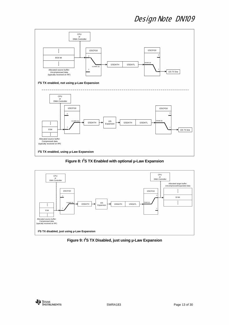
The overall functionality of I2S TX/RX, with optional µ-Law encoding, and optional I2S I/O usage, is shown in Figure 6, Figure 7, Figure 8, and Figure 9. The typical configuration in Figure 6 is that the I2S peripheral reads samples through the enabled I2S RX path, compresses the sample (if µ-Law compression is enabled) before writing it to the I2SDATH register. The application (CPU or DMA controller) then reads the I2SDATH register and stores this sample in an allocated target buffer, which is typically to be processed and transmitted on RF later. Figure 8 shows a typical I2S TX configuration, where the application writes compressed/uncompressed source data (typically received by RF) to the I2S peripheral, which then applies µ-Law Expansion if enabled, and finally outputs the I2SDATL/H data through the I2S TX path, if enabled. As described in the “µ-Law Compression and Expansion” section SoC data sheets ([1] and [2]), it is also possible to execute µ-Law encoding without actually using the I2S I/O interface. This is shown in Figure 7, and Figure 9, and generally requires that only one of the flags I2SCFG0.ULAWE/ULAWC be 1 while the I2SCFG0.ENAB bit is 0.

Design Note DN109
SWRA183 Page 12 of 30
I2SDATH
I2S RX line
I2SDATL
I2SCFG0
ENAB (0)
0
1
Allocated target buffer:Uncompressed data
(typically to be transmitted on RF)
CPUor
DMA Controller
I2SCFG0
ULAWC (4)
1
08/16 bit
I2SDATHI2S
CompressionI2S RX line
I2SCFG0
ENAB (0)
0
1
CPUor
DMA Controller
I2SCFG0
ULAWC (4)
1
0Allocated target buffer:
Compressed data(typically to be transmitted on RF)
8 bit
I2S RX enabled, using µ-Law Compression
I2S RX enabled, not using µ-Law Compression
Figure 6: I2S RX Enabled with optional µ-Law Compression
16 bit
Allocated source buffer:Uncompressed data
I2SCFG0
ENAB (0)
0
1
CPUor
DMA Controller
I2SCFG0
ULAWC (4)
1
0
I2SDATHI2S
Compression
CPUor
DMA Controller
Allocated target buffer:Compressed data
(typically to be transmitted on RF)
8 bit
I2S RX disabled, just using µ-Law Compression
Figure 7: I2S RX Disabled, just using µ-Law Compression (no I/O usage)
Design Note DN109
SWRA183 Page 13 of 30
Allocated source buffer:Uncompressed data
(typically received on RF)
CPUor
DMA Controller
I2S TX line
I2SDATH I2SDATL
8/16 bit
I2SCFG0
ENAB (0)
1
0
I2SCFG0
ULAWE (5)
0
1
I2S TX enabled, not using µ-Law Expansion
I2S TX line
I2S TX enabled, using µ-Law Expansion
I2SDATH I2SDATL
I2SCFG0
ENAB (0)
1
0
I2SCFG0
ULAWE (5)
0
1
Allocated source buffer:Compressed data
(typically received on RF)
8 bit
I2SExpansionI2SDATH
CPUor
DMA Controller
Figure 8: I2S TX Enabled with optional µ-Law Expansion
I2SDATH I2SDATL
I2SCFG0
ENAB (0)
1
0
I2SCFG0
ULAWE (5)
0
1
Allocated source buffer:Compressed data
(typically received on RF)
8 bit
I2SExpansion
16 bit
Allocated target buffer:Uncompressed/expanded data
CPUor
DMA Controller
I2SDATH
CPUor
DMA Controller
I2S TX disabled, just using µ-Law Expansion
Figure 9: I2S TX Disabled, just using µ-Law Expansion

Design Note DN109
SWRA183 Page 14 of 30
The required code for initializing the I2S protocol is shown in Figure 10, and it implements the following main steps:
1. Set the I2S Word size in I2SCFG1.WORDS according to the desired number bits for each I2S word transfer.
2. For RX/TX Master set I2SCFG0.MASTER. For RX/TX Slave clear I2SCFG0.MASTER. Note that the Master drives the I2S clock; even if the slave writes to its I2SDATL/H register(s) nothing will actually be output on the slave’s I2S TX pin as long as the external Master is disabled.
3. For RX/TX Mono set I2SCFG0.RXMONO/TXMONO. For RX/TX Stereo clear I2SCFG0.RXMONO/TXMONO.
4. For enabling µ-Law encoding in RX/TX set I2SCFG0.ULAWC/ULAWE. For disabling µ-Law encoding in RX/TX clear I2SCFG0.ULAWC/ULAWE.
Figure 10: Initializing the I2S Protocol
// C language code: // This function initializes the main I2S Protocol settings; // word size, mode (Master/Slave), format (Mono/Stereo), and encoding // (µ-Law compression/expansion). For simplicity this function assumes // same I2S protocol settings in I2S RX and TX. The application must // call this function, using the below defines. // Valid input to the "i2sMode", "i2sFormat", and "i2sEncode" arguments: #define I2S_MODE_SLAVE 0 #define I2S_MODE_MASTER 1 #define I2S_FORMAT_STEREO 0 #define I2S_FORMAT_MONO 1 #define I2S_ENCODE_NONE 0 #define I2S_ENCODE_ULAWC 1 #define I2S_ENCODE_ULAWE 2 void i2sInitProtocol(unsigned char i2sWordSize, unsigned char i2sMode, unsigned char i2sFormat, unsigned char i2sEncode) { // Set I2S Word size (I2SCFG1.WORDS) I2SCFG1 = (I2SCFG1&~0xF8) | (((i2sWordSize-1)&0x1F)<<3); // If I2S Master, then set I2SCFG0.MASTER if (i2sMode == I2S_MODE_MASTER) { I2SCFG0 |= 0x02; // Else (I2S Slave), then clear I2SCFG0.MASTER } else { I2SCFG0 &= ~0x02; } // If I2S Mono, then set I2SCFG0.RXMONO/TXMONO if (i2sFormat == I2S_FORMAT_MONO) { I2SCFG0 |= (0x04 | 0x08); // Else (I2S Stereo), then clear I2SCFG0.RXMONO/TXMONO } else { I2SCFG0 &= ~(0x04 | 0x08); } // If µ-Law TX encoding (Expansion) desired, then set I2SCFG0.ULAWE if (i2sEncode == I2S_ENCODE_ULAWE) { I2SCFG0 |= 0x20; // Else if µ-Law RX encoding (Compression) desired, then set I2SCFG0.ULAWC } else if (i2sEncode == I2S_ENCODE_ULAWC) { I2SCFG0 |= 0x10; // Else (µ-Law encoding not desired) clear I2SCFG0.ULAWC/ULAWE } else { I2SCFG0 &= ~(0x20 | 0x10); } }

Design Note DN109
SWRA183 Page 15 of 30
4.2 Using the I2S Peripheral without DMA Support
Using the I2S without support from the DMA controller means that the CPU must handle all data transfers between the I2S peripheral and SoC memory. During I2S transfers the CPU will not be able to perform other tasks, except from ISRs. In order to process the I2S communication without DMA support the application can either poll the I2S Interrupt Flag or implement a designated I2S ISR. Both methods imply that the application/CPU must monitor the I2S interrupt request flags I2SSTAT.TXIRQ/RXIRQ.
4.2.1 Processing I2S Communication using I2S Polling
The following section shows how to control the I2S communication, using polling of the interrupt request flags. This method typically implies that the application defers all other tasks (apart from ISRs) while processing the I2S communication accessing the I2SDATH/L and I2SSTAT.TXIRQ/RXIRQ.
4.2.1.1 I2S TX Processing using I2S Polling
The required code for I2S TX, with polling, is shown in Figure 11 and Figure 12 and implements the following main steps:
1. Allocate I2S TX buffer for the associated source samples. The data in this buffer has typically been received by RF, and then processed prior to the I2S TX operation.
2. Disable the I2S TX interrupt (this instruction will not mask the generation of the interrupt request flags, used for polling I2S TX complete; ref. Figure 2), and enable the I2S peripheral (in master mode this implies that the I2S clock starts to run).
3. Enable the I2S peripheral. If configured as Master, this will start the I2S master clock, and thus the I2S peripheral will immediately start accessing the I2SDATl/H register(s).
4. Before each write access to the appropriate I2SDATl/H register(s), poll I2SSTAT.TXIRQ to wait until I2S peripheral has transmitted the last word.
5. Write the relevant (left/right) I2S word to the appropriate I2SDATl/H register(s), according to the applied I2S word size, format (mono/stereo), and µ-Law encoding (Expansion). This should be done according to the code in Figure 11.
6. Apply code in Figure 12 to send an entire allocated source buffer. This function outputs the source buffer on the I2S TX line, word-by-word, by repeated calls to the function in Figure 11 until end of source buffer.
Note: One of the objectives for the code examples in this section is to show what configuration/status registers are involved in the different operating modes (Mono/Stereo, and µ-Law compression/expansion). The chosen implementation typically supports I2S sample rates up to 8 kHz. For higher I2S sample rates the code should be optimized in such a way that it assumes a specific operating mode and thus simply access the relevant I2SDATH/L registers without reading the corresponding configuration registers (I2SCFGx) first. Alternatively use DMA support, as described in section 4.3.

Design Note DN109
SWRA183 Page 16 of 30
Figure 11: I2S TX Word Processing using I2S Polling
// C language code: // This function sends a single I2S sample on the I2S TX line, according // to the applied I2S format; Mono/Stereo, I2S encoding; µ-Law Expansion. // In Mono mode the application should, for implementation convenience, // input the left word also as the right word. This function automatically // interfaces the appropriate I2SDATL/H register(s) according to the applied // I2S protocol. Note that, before this function is called the application // must execute the I2S initialization code in Figure 3, Figure 5, and // Figure 10. void i2sSendSample(unsigned short i2sLeftWord, unsigned short i2sRightWord) { unsigned char i; // Disable I2S TX interrupt (I2SCFG0.TXIEN = 0), // and enable I2S interface (I2SCFG0.ENAB = 1) I2SCFG0 = (I2SCFG0 & ~0x80) | 0x01; // If Mono mode (I2SCFG0.TXMONO = 1) if (I2SCFG0 & 0x08) { // Poll I2SSTAT.TXIRQ to wait until I2S has transmitted the last word while ( !(I2SSTAT&0x08) ); // If µ-Law expansion enabled (I2SCFG0.ULAWE = 1) // or Word size (I2SCFG1.WORDS) < 9 bits if ((I2SCFG0 & 0x20) || (((I2SCFG1 & 0xF8) >> 3) < 9) ) { // Write left word only, to I2SDATH only I2SDATH = i2sLeftWord; // Else, µ-Law expansion disabled (I2SCFG0.ULAWE = 0) // and Word size (I2SCFG1.WORDS) > 8 bits } else { // Write left word only, to I2SDATL/H I2SDATL = i2sLeftWord & 0x00FF; I2SDATH = (i2sLeftWord >> 8) & 0x00FF; } // Else, Stereo mode (I2SCFG0.TXMONO = 0) } else { // If µ-Law expansion enabled (I2SCFG0.ULAWE = 1) // or Word size (I2SCFG1.WORDS) < 9 bits if ((I2SCFG0 & 0x20) || (((I2SCFG1 & 0xF8) >> 3) < 9) ) { // Write left/right word to I2SDATL/H registers for (i = 0; i < 2; i++) { // Poll I2SSTAT.TXIRQ to wait until I2S has transmitted the last word while ( !(I2SSTAT & 0x08)); // If I2S left channel ready, write left word, to I2SDATH only if (!(I2SSTAT & 0x20)) { I2SDATH = i2sLeftWord; // Else, I2S right channel ready, write right word to I2SDATH only } else { I2SDATH = i2sRightWord; } } // Else, µ-Law expansion disabled (I2SCFG0.ULAWE = 0) // and Word size (I2SCFG1.WORDS) > 8 bits } else { // Write left/right word to I2SDATL/H registers for (i = 0; i < 2; i++) { // Poll I2SSTAT.TXIRQ to wait until I2S has transmitted the word while ( !(I2SSTAT & 0x08)); // If I2S left channel ready, write left word to I2SDATL/H if (!(I2SSTAT & 0x20)) { I2SDATL = i2sLeftWord&0x00FF; I2SDATH = (i2sLeftWord >> 8) & 0x00FF; // Else, I2S right channel ready, write right word to I2SDATL/H } else { I2SDATL = i2sRightWord & 0x00FF; I2SDATH = (i2sRightWord >> 8) & 0x00FF; } } } } }

Design Note DN109
SWRA183 Page 17 of 30
Figure 12: I2S TX Buffer Processing using I2S Polling
4.2.1.2 I2S RX processing using I2S Polling
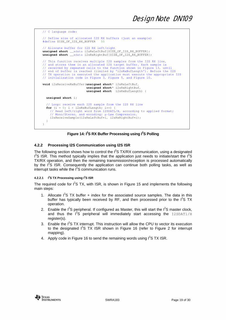
The required code for I2S RX, with polling, is shown in Figure 13 and Figure 14 and implements the following main steps:
1. Allocate I2S RX buffer for the associated target samples. This buffer is typically to be processed, and then transmitted by RF after the I2S RX operation has completed.
2. Disable the I2S RX interrupt (this instruction will not mask the generation of the interrupt request flags, used for polling I2S RX complete; ref. Figure 2).
3. Enable the I2S peripheral. If configured as Master, this will start the I2S master clock, and thus the I2S peripheral will immediately start accessing the I2SDATl/H register(s).
4. Poll I2SSTAT.RXIRQ to wait until I2S peripheral has received the word. 5. Read the appropriate I2SDATl/H register(s), according to the applied I2S word size,
format (Mono/Stereo), and µ-Law encoding (Expansion), and store the contents in the relevant (left/right) allocated I2S word. This should be done according to the code in Figure 13.
6. In Stereo mode, poll I2SSTAT.RXIRQ again to wait until I2S peripheral has received another word (representing the opposite I2S channel). Then apply step (4) to read the I2S word.
7. Apply the code in Figure 14 to receive multiple I2S samples and store them in an allocated target buffer. This function reads the input from the I2S RX line, word-by-word, by repeated calls to the function in Figure 14 until end of target buffer.
// C language code: // Define size of allocated I2S TX buffer (just an example) #define SIZE_OF_I2S_TX_BUFFER 50 // Allocate buffer for I2S TX left/right unsigned short __xdata i2sTxLeftBuffer[SIZE_OF_I2S_TX_BUFFER]; unsigned short __xdata i2sTxRightBuffer[SIZE_OF_I2S_TX_BUFFER]; // This function sends an allocated I2S source buffer on the I2S TX line. // Each sample is transmitted by repeated calls to the function shown in // Figure 11, until end of buffer is reached (limited by "i2sTxBufLength"). // Before the I2S TX operation is executed the application must execute the // appropriate I2S initialization code in Figure 3, Figure 5, and Figure 10. void i2sSendTxBuffer(unsigned short* i2sTxLeftBuf, unsigned short* i2sTxRightBuf, unsigned short i2sTxBufLength) { unsigned short i; // Loop: send each I2S sample on the I2S TX line for (i = 0; i < i2sTxBufLength; i++) { // Write left/write word to I2SDATL/H according to applied format; // Mono/Stereo, and encoding; µ-Law Expansion. i2sSendSample(i2sTxLeftBuf[i], i2sTxRightBuf[i]); } }

Design Note DN109
SWRA183 Page 18 of 30
Figure 13: I2S RX Word Processing using I2S Polling
// C language code: // This function receives a single I2S sample on the I2S RX line, according // to the applied I2S format; Mono/Stereo, I2S encoding; µ-Law Compression. // In Mono mode the application should, for implementation convenience, // use the left word reference also for the right word. This function will // automatically interface the appropriate I2SDATL/H register(s) according // to the applied I2S protocol. Note that, before this function is called // the application must execute the I2S initialization code in Figure 3, // Figure 5, and Figure 10. void i2sReceiveSample(unsigned short* i2sLeftWord, unsigned short* i2sRightWord) { unsigned char i; // Disable I2S RX interrupt (I2SCFG0.RXIEN = 0), // and enable I2S interface (I2SCFG0.ENAB = 1) I2SCFG0 = (I2SCFG0 & ~0x40) | 0x01; // If Mono mode (I2SCFG0.RXMONO = 1) if (I2SCFG0 & 0x04) { // Poll I2SSTAT.RXIRQ to wait until I2S has received a word while (!(I2SSTAT & 0x04)); // If µ-Law compression enabled (I2SCFG0.ULAWC = 1) // or Word size (I2SCFG1.WORDS) < 9 bits if ((I2SCFG0 & 0x10) || (((I2SCFG1 & 0xF8) >> 3) < 9) ) { // Store I2SDATH only *i2sLeftWord = I2SDATH; // Else, µ-Law compression disabled (I2SCFG0.ULAWC = 0) // or Word size (I2SCFG1.WORDS) > 8 bits } else { // Store I2SDATL/H *i2sLeftWord = I2SDATL; *i2sLeftWord |= ((unsigned short)I2SDATH << 8); } // Else, Stereo mode (I2SCFG0.RXMONO = 0) } else { // If µ-Law compression enabled (I2SCFG0.ULAWC = 1) // or Word size (I2SCFG1.WORDS) < 9 bits if ((I2SCFG0 & 0x10) || (((I2SCFG1 & 0xF8) >> 3) < 9) ) { // Store I2SDATH according to target (left/right) channel: for (i = 0; i < 2; i++) { // Poll I2SSTAT.RXIRQ to wait until I2S has received a word while (!(I2SSTAT & 0x04)); if (!(I2SSTAT & 0x10)) { *i2sLeftWord = I2SDATH; } else { *i2sRightWord = I2SDATH; } } // Else, µ-Law compression disabled (I2SCFG0.ULAWC = 0) // or Word size (I2SCFG1.WORDS) > 8 bits } else { // Store I2SDATL/H according to target (left/right) channel: for (i = 0; i < 2; i++) { // Poll I2SSTAT.RXIRQ to wait until I2S has received a word while (!(I2SSTAT & 0x04)); if (!(I2SSTAT & 0x10)) { *i2sLeftWord = I2SDATL; *i2sLeftWord |= ((unsigned short)I2SDATH << 8); } else { *i2sRightWord = I2SDATL; *i2sRightWord |= ((unsigned short)I2SDATH << 8); } } } } }
Design Note DN109
SWRA183 Page 19 of 30
Figure 14: I2S RX Buffer Processing using I2S Polling
4.2.2 Processing I2S Communication using I2S ISR
The following section shows how to control the I2S TX/RX communication, using a designated I2S ISR. This method typically implies that the application just needs to initiate/start the I2S TX/RX operation, and then the remaining transmission/reception is processed automatically by the I2S ISR. Consequently the application can continue both polling tasks, as well as interrupt tasks while the I2S communication runs.
4.2.2.1 I2S TX Processing using I2S ISR
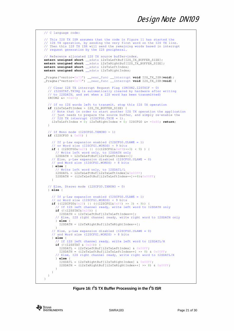
The required code for I2S TX, with ISR, is shown in Figure 15 and implements the following main steps:
1. Allocate I2S TX buffer + index for the associated source samples. The data in this buffer has typically been received by RF, and then processed prior to the I2S TX operation.
2. Enable the I2S peripheral. If configured as Master, this will start the I2S master clock, and thus the I2S peripheral will immediately start accessing the I2SDATl/H register(s).
3. Enable the I2S TX interrupt. This instruction will allow the CPU to vector its execution to the designated I2S TX ISR shown in Figure 16 (refer to Figure 2 for interrupt mapping).
4. Apply code in Figure 16 to send the remaining words using I2S TX ISR.
// C language code: // Define size of allocated I2S RX buffers (just an example) #define SIZE_OF_I2S_RX_BUFFER 50 // Allocate buffer for I2S RX left/right unsigned short __xdata i2sRxLeftBuf[SIZE_OF_I2S_RX_BUFFER]; unsigned short __xdata i2sRxRightBuf[SIZE_OF_I2S_RX_BUFFER]; // This function receives multiple I2S samples from the I2S RX line, // and stores them in an allocated I2S target buffer. Each sample is // received by repeated calls to the function shown in Figure 13, until // end of buffer is reached (limited by "i2sRxBufLength"). Before the I2S // TX operation is executed the application must execute the appropriate I2S // initialization code in Figure 3, Figure 5, and Figure 10. void i2sReceiveRxBuffer(unsigned short* i2sRxLeftBuf, unsigned short* i2sRxRightBuf, unsigned short i2sRxBufLength) { unsigned short i; // Loop: receive each I2S sample from the I2S RX line for (i = 0; i < i2sRxBufLength; i++) { // Read left/right word from I2SDATL/H, according to applied format; // Mono/Stereo, and encoding; µ-Law Compression. i2sReceiveSample(i2sRxLeftBuf+i, i2sRxRightBuf+i); } }

Design Note DN109
SWRA183 Page 20 of 30
Figure 15: Initializing I2S TX Word Processing for the I2S ISR
// C language code: // This function starts the I2S TX operation by simply enabling the // corresponding I2S interrupt, and leave the sample transmission to // the I2S ISR shown in Figure 16. Before this function is called the // application must initialize the I2S peripheral according to the code // shown in Figure 3, Figure 5, and Figure 10. // Define I2S RX/TX buffer size (just an example) #define I2S_TX_BUFFER_SIZE 50 // Allocate source buffer+index for I2S TX. unsigned short __xdata i2sTxLeftBuf[I2S_TX_BUFFER_SIZE]; unsigned short __xdata i2sTxRightBuf[I2S_TX_BUFFER_SIZE]; unsigned short __xdata i2sTxLeftIndex; unsigned short __xdata i2sTxRightIndex; void i2sStartTxForIsr(void) { // Initialize the I2S TX buffer indexes. i2sRxLeftIndex = 0; i2sRxRightIndex = 0; // Set I2SCFG0.TXIE = 1, IEN0.EA = 1, and IEN2.I2STXIE = 1 to enable // I2S TX CPU interrupt. Set I2SCFG0.ENAB = 1 to enable the I2S interface. // Note that once the I2S TX interrupt is enabled and the I2S master clock // has completed an I2S word transfer the CPU will immediately vector its // execution to the corresponding I2S ISR in Figure 16. I2SCFG0 |= (0x80 | 0x01); IEN2 |= 0x08; IEN0 |= 0x80; // At this point the I2S ISR, shown in Figure 16, will automatically take // over and transmit the remaining bytes in the I2S TX source buffer. }
Design Note DN109
SWRA183 Page 21 of 30
Figure 16: I2S TX Buffer Processing in the I2S ISR
// C language code: // This I2S TX ISR assumes that the code in Figure 11 has started the // I2S TX operation, by sending the very first word on the I2S TX line. // Then this I2S TX ISR will send the remaining words based in interrupt // request generation by the I2S peripheral. // Reference allocated I2S TX source buffer+index. extern unsigned short __xdata i2sTxLeftBuf[I2S_TX_BUFFER_SIZE]; extern unsigned short __xdata i2sTxRightBuf[I2S_TX_BUFFER_SIZE]; extern unsigned short __xdata i2sTxLeftIndex; extern unsigned short __xdata i2sTxRightIndex; _Pragma("vector=0x73") __near_func __interrupt void I2S_TX_ISR(void); _Pragma("vector=0x73”) __near_func __interrupt void I2S_TX_ISR(void) { // Clear I2S TX interrupt Request Flag (IRCON2.I2STXIF = 0) // (I2SSTAT.TXIRQ is automatically cleared by hardware after writing // to I2SDATH, and set when a I2S word has been transmitted) IRCON2 &= ~0x04; // If no I2S words left to transmit, stop this I2S TX operation if (i2sTxLeftIndex > I2S_TX_BUFFER_SIZE) { // Note that in order to start another I2S TX operation the application // just needs to prepare the source buffer, and simply re-enable the // I2S TX interrupt (I2SCFG0.TXIE = 1). i2sTxLeftIndex = 0; i2sTxRightIndex = 0; I2SCFG0 &= ~0x80; return; } // If Mono mode (I2SCFG0.TXMONO = 1) if (I2SCFG0 & 0x08) { // If µ-Law expansion enabled (I2SCFG0.ULAWE = 1) // or Word size (I2SCFG1.WORDS) < 9 bits if ( (I2SCFG0&0x20) || (((I2SCFG1&0xF8)>>3) < 9) ) { // Write left word only, to I2SDATH only I2SDATH = i2sTxLeftBuf[i2sTxLeftIndex++]; // Else, µ-Law expansion disabled (I2SCFG0.ULAWE = 0) // and Word size (I2SCFG1.WORDS) > 8 bits } else { // Write left word only, to I2SDATL/L I2SDATL = i2sTxLeftBuf[i2sTxLeftIndex]&0x00FF; I2SDATH = (i2sTxLeftBuf[i2sTxLeftIndex++]>>8)&0x00FF; } // Else, Stereo mode (I2SCFG0.TXMONO = 0) } else { // If µ-Law expansion enabled (I2SCFG0.ULAWE = 1) // or Word size (I2SCFG1.WORDS) < 9 bits if ((I2SCFG0&0x20) || (((I2SCFG1&0xF8) >> 3) < 9)) { // If I2S left channel ready, write left word to I2SDATH only if (!(I2SSTAT&0x20)) { I2SDATH = i2sTxLeftBuf[i2sTxLeftIndex++]; // Else, I2S right channel ready, write right word to I2SDATH only } else { I2SDATH = i2sTxRightBuf[i2sTxRightIndex++]; } // Else, µ-Law expansion disabled (I2SCFG0.ULAWE = 0) // and Word size (I2SCFG1.WORDS) > 8 bits } else { // If I2S left channel ready, write left word to I2SDATL/H if (!(I2SSTAT & 0x20)) { I2SDATL = i2sTxLeftBuf[i2sTxLeftIndex] & 0x00FF; I2SDATH = (i2sTxLeftBuf[i2sTxLeftIndex++] >> 8) & 0x00FF; // Else, I2S right channel ready, write right word to I2SDATL/H } else { I2SDATL = i2sTxRightBuf[i2sTxRightIndex] & 0x00FF; I2SDATH = (i2sTxRightBuf[i2sTxRightIndex++] >> 8) & 0x00FF; } } } }

Design Note DN109
SWRA183 Page 22 of 30
4.2.2.2 I2S RX Processing using I2S ISR
The required code for I2S RX, with ISR, is shown in Figure 17 and Figure 18 and implements the following main steps:
1. Allocate I2S RX buffer + index for the associated target samples. This buffer is typically to be processed, and then transmitted by RF after the I2S RX operation has completed.
2. Enable the I2S peripheral. If configured as Master, this will start the I2S master clock, and thus the I2S peripheral will immediately start accessing the I2SDATl/H register(s).
3. Enable the I2S RX interrupt to allow the CPU to automatically vector its execution to the designated I2S RX ISR, shown in Figure 18, once the I2S peripheral has received a word (refer to Figure 2 for interrupt mapping).
4. Receive the remaining words using I2S RX ISR, as shown in Figure 18.
Figure 17: Initializing I2S RX Word Processing for the I2S ISR
// C language code: // This function starts the I2S RX operation, by simply enabling the // corresponding I2S interrupt, and leave the sample reception to the // I2S ISR shown in Figure 18. Before this function is called the // application must initialize the I2S peripheral according to the // code shown in Figure 3, Figure 5, and Figure 10. // Define I2S RX buffer size (just an example) #define I2S_RX_BUFFER_SIZE 50 // Allocate source buffer+index for I2S RX. unsigned short __xdata i2sRxLeftBuf[I2S_RX_BUFFER_SIZE]; unsigned short __xdata i2sRxRightBuf[I2S_RX_BUFFER_SIZE]; unsigned short __xdata i2sRxLeftIndex; unsigned short __xdata i2sRxRightIndex; void i2sStartRxForIsr(void) { // Initialize the I2S RX buffer indexes. i2sRxLeftIndex = 0; i2sRxRightIndex = 0; // Set I2SCFG0.RXIE = 1, IEN0.EA = 1, and IEN0.I2SRXIE = 1 to enable // I2S TX CPU interrupt. Set I2SCFG0.ENAB to enable the I2S interface. I2SCFG0 |= (0x40 | 0x01); IEN0 |= (0x80 | 0x08); // At this point the CPU will automatically vector its execution to // the I2S RX ISR, shown in Figure 18, once the I2S peripheral has // received a word on the I2S RX line. }

Design Note DN109
SWRA183 Page 23 of 30
Figure 18: I2S RX Buffer Processing in the I2S ISR
// C language code: // This I2S RX ISR assumes that the code in Figure 17 has started the // I2S RX operation, by enabling the I2S RX interrupt. Then this I2S RX ISR // will receive the words based on interrupt request generation by the // I2S peripheral. // Reference allocated I2S RX target buffer+index. extern unsigned short __xdata i2sRxLeftBuf[I2S_RX_BUFFER_SIZE]; extern unsigned short __xdata i2sRxRightBuf[I2S_RX_BUFFER_SIZE]; extern unsigned short __xdata i2sRxLeftIndex; extern unsigned short __xdata i2sRxRightIndex; _Pragma("vector=0x1B") __near_func __interrupt void I2S_RX_ISR(void); _Pragma("vector=0x1B") __near_func __interrupt void I2S_RX_ISR(void) { // Clear I2S RX interrupt Request Flag (TCON.I2SRXIF = 0) // (I2SSTAT.RXIRQ is automatically cleared by hardware after reading // I2SDATH, and set when the I2S peripheral has received a word) TCON &= ~0x80; // If all I2S words received, stop this I2S RX operation if (i2sRxLeftIndex > I2S_RX_BUFFER_SIZE) { // Note that in order to start another I2S RX operation the application // just needs to prepare the source buffer, and simply re-enable the // I2S RX interrupt (I2SCFG0.RXIE = 1). i2sRxLeftIndex = 0; i2sRxRightIndex = 0; I2SCFG0 &= ~0x40; return; } // If Mono mode (I2SCFG0.RXMONO = 1) if (I2SCFG0 & 0x04) { // If µ-Law compression enabled (I2SCFG0.ULAWC = 1) // or Word size (I2SCFG1.WORDS) < 9 bits if ( (I2SCFG0&0x10) || (((I2SCFG1&0xF8)>>3) < 9) ) { // Store I2SDATH only i2sRxLeftBuf[i2sRxLeftIndex++] = I2SDATH; // Else, µ-Law compression disabled (I2SCFG0.ULAWC = 0) // and Word size (I2SCFG1.WORDS) > 8 bits } else { // Store I2SDATL/H i2sRxLeftBuf[i2sRxLeftIndex] = I2SDATL; i2sRxLeftBuf[i2sRxLeftIndex++] |= ((unsigned short)I2SDATH << 8); } // Else, Stereo mode (I2SCFG0.RXMONO = 0) } else { // If µ-Law compression enabled (I2SCFG0.ULAWC = 1) // or Word size (I2SCFG1.WORDS) < 9 bits if ( (I2SCFG0&0x10) || (((I2SCFG1&0xF8)>>3) < 9) ) { // Store I2SDATH according to target (left/right) channel if ( !(I2SSTAT&0x10) ) { i2sRxLeftBuf[i2sRxLeftIndex++] = I2SDATH; } else { i2sRxRightBuf[i2sRxRightIndex++] = I2SDATH; } // Else, µ-Law compression disabled (I2SCFG0.ULAWC = 0) // and Word size (I2SCFG1.WORDS) > 8 bits } else { // Store I2SDATL/H according to target (left/right) channel if ( !(I2SSTAT&0x10) ) { i2sRxLeftBuf[i2sRxLeftIndex] = I2SDATL; i2sRxLeftBuf[i2sRxLeftIndex++] |= ((unsigned short)I2SDATH << 8); } else { i2sRxRightBuf[i2sRxRightIndex] = I2SDATL; i2sRxRightBuf[i2sRxRightIndex++] |= ((unsigned short)I2SDATH << 8); } } } }

Design Note DN109
SWRA183 Page 24 of 30
4.3 Using the I2S Peripheral with DMA Support
In order to use the DMA controller to support the I2S peripheral, typically two DMA channels must be allocated and configured: one for downloading data from SoC memory to the I2S peripheral (TX), and another for uploading data from the I2S peripheral to SoC memory (RX). Please refer to the “DMA Controller” section in the SoC Data Sheets ([1] and [2]) for more detailed information about the DMA controller.
For I2S TX/RX Stereo processing with DMA support the application must typically organize all the source samples (left and right) in one single buffer, and in alternating sequence; a left channel sample should follow directly after a right channel sample (left, right, left, right, etc.). The reason is that, during operation, the DMA controller is only able to increment/decrement its memory pointer. This means that once the DMA controller has started to transfer a range of words between the allocated source/target buffer and the I2SDATL/H registers it is not able to change the entire SRCADDRx/DESTADDRx pointers in the DMA descriptor.
4.3.1 Allocating DMA Descriptor for I2S RX/TX
Before the I2S peripheral can transmit/receive with DMA support, the application must allocate associated DMA descriptors; one for RX, and one TX. The required code is shown in Figure 19:
Figure 19: Allocating Buffers and DMA Descriptors for I2S RX/TX
// C language code: // Define data structure for DMA descriptor: typedef struct { unsigned char SRCADDRH; // High byte of the source address unsigned char SRCADDRL; // Low byte of the source address unsigned char DESTADDRH; // High byte of the destination address unsigned char DESTADDRL; // Low byte of the destination address unsigned char VLEN : 3; // Length configuration unsigned char LENH : 5; // High byte of fixed length unsigned char LENL : 8; // Low byte of fixed length unsigned char WORDSIZE : 1; // Number of bytes per transfer element unsigned char TMODE : 2; // DMA trigger mode (e.g. single or repeated) unsigned char TRIG : 5; // DMA trigger; I2S RX/TX unsigned char SRCINC : 2; // Number of source address increments unsigned char DESTINC : 2; // Number of destination address increments unsigned char IRQMASK : 1; // DMA interrupt mask unsigned char M8 : 1; // Number of desired bit transfers in byte mode unsigned char PRIORITY : 2; // The DMA memory access priority } DMA_DESC; // Allocate DMA descriptor for I2S RX/TX: // Note that, since the DMA controller only offers one address/reference // register for DMA channels 1 - 4, the DMA controller expects the // allocated descriptors for those DMA channels to be located in direct // address succession. This is typically relevant when the application has // already allocated DMA channel 0, and 1, for other purposes than I2S // support. DMA_DESC __xdata i2sDmaRxTxCh[2]; // Note that in I2S TX Stereo the application must organize the I2S source // samples in an alternating sequence; left word, right word, left word, etc. // The reason is that the DMA controller is only able to increment/decrement // its memory pointer during operation; once the DMA controller has started // a block transfer it is not able to change the entire SRCADDRx/DESTADDRx // pointers in the DMA descriptor. This is only possible when the associated // DMA channel is idle.

Design Note DN109
SWRA183 Page 25 of 30
4.3.2 Processing I2S Communication with DMA Support
The following section shows how to control the I2S RX/TX communication using DMA support. This method typically implies that the application just needs to initiate/start the I2S TX/RX, and then the remaining word transfers are processed automatically by the DMA controller. The application can continue both polling tasks, as well as interrupt tasks while the I2S communication goes on.
Note that the DMA controller has no knowledge of the I2S WS (channel select) signal state (left/right). The only control signals flowing from the I2S peripheral to the DMA controller are the I2S RX/TX interrupt request flags, which are used solely to trigger a DMA word transfer between SoC memory and the I2SDATL/H registers. Thus before allowing the I2S peripheral to trigger the DMA word transfer the application must initially wait until the WS signal state fits the channel associated with the very first word in the allocated I2S RX/TX buffer. The required code for I2S RX/TX, using DMA support (shown in Figure 19, Figure 20, Figure 21, and Figure 22) implements the following main steps:
1. Allocate I2S RX/TX buffer + index for the associated source samples. The data in the I2S TX buffer has typically been received by RF, and then processed prior to the I2S TX operation. The data in the I2S RX buffer is typically to be transmitted on RF after the I2S RX operation.
2. Define and allocate data structures for DMA channel configuration (descriptors used to set up a DMA channel for transferring data between SoC memory and the I2S peripheral.
3. Enable the I2S peripheral. If configured as Master, this will start the I2S master clock, and thus the I2S peripheral will immediately start accessing the I2SDATl/H register(s).
4. In I2S RX/TX stereo mode, wait until the I2S WS signal state (left/right) fits the channel associated with the very first word in the allocated I2S RX/TX buffer.
5. Start the I2S RX/TX operation by arming the associated DMA channel. Provided that the I2S clock is running at this point the I2S peripheral will automatically trigger the DMA controller to transfer a word between SoC memory and the I2SDATL/H registers once the I2S peripheral has transmitted/received the word, which again triggers another DMA word transfer. This sequence continues until the DMA controller has completed the programmed number of word transfers.
6. Once the DMA controller has completed the defined range of word transfers, the application can start another I2S RX/TX operation by simply re-arming the associated DMA channel. For efficient data streaming (typically between RF and I2S) the application could for example, implement the I2S re-start mechanism in a designated DMA ISR, as shown in Figure 22, thus isolating the I2S RX/TX operation as much as possible from the main application code.

Design Note DN109
SWRA183 Page 26 of 30
Figure 20: I2S TX Initialization using DMA Support
// C language code: // This function sets up and starts the I2S TX transmission. // Before this function is called the application must perform initialization // by executing the code in Figure 3, Figure 5, and Figure 10. void i2sStartTxDmaChan( DMA_DESC *i2sDmaTxDescr, unsigned char i2sDmaTxChan, unsigned short* i2sTxBuf, unsigned short i2sTxBufSize, unsigned char i2sWordLength) { // Set source pointer (I2S TX buffer address) for I2S TX DMA channel, // and total number DMA word transfer (according to I2S TX buffer size). i2sDmaTxDescr.SRCADDRH = i2sTxBuf >> 8; i2sDmaTxDescr.SRCADDRL = i2sTxBuf; i2sDmaTxDescr.LENH = (i2sTxBufSize >> 8) & 0xFF; i2sDmaTxDescr.LENL = i2sTxBufSize & 0xFF; i2sDmaTxDescr.VLEN = 0x00; // Use fixed length DMA transfer count // Set DMA transfer size and destination pointer according // to I2S Word size and µ-Law encoding if ((I2SCFG0&0x20) || (((I2SCFG1 & 0xF8) >> 3) < 9)) { i2sDmaTxDescr.WORDSIZE = 0x00; // Perform 1-byte transfers i2sDmaTxDescr.DESTADDRH = 0xDF; // High byte Address of I2SDATH i2sDmaTxDescr.DESTADDRL = 0x43; // Low byte Address of I2SDATH } else { i2sDmaTxDescr.WORDSIZE = 0x01; // Perform 2-byte transfers i2sDmaTxDescr.DESTADDRH = 0xDF; // High byte Address of I2SDATL i2sDmaTxDescr.DESTADDRL = 0x42; // Low byte Address of I2SDATL } i2sDmaTxDescr.TMODE = 0x00; // Transfer a single word after each i2sDmaTxDescr.TRIG = 28; // DMA word trigger = I2S TX i2sDmaTxDescr.SRCINC = 0x01; // Increment source pointer by 1 word // address after each transfer. i2sDmaTxDescr.DESTINC = 0x00; // Do not increment destination pointer: // points to I2S I2SDATH/L register. i2sDmaTxDescr.IRQMASK = 0x01; // Enable DMA interrupt to the CPU i2sDmaTxDescr.M8 = 0x00; // Use all 8 bits for transfer count i2sDmaTxDescr.PRIORITY = 0x00; // DMA memory access has low priority // Link DMA descriptor with its corresponding DMA configuration register. if (i2sDmaTxChan < 1) { DMA0CFGH = (unsigned char)((unsigned short)i2sDmaTxDescr >> 8); DMA0CFGL = (unsigned char)((unsigned short)i2sDmaTxDescr & 0x00FF); } else { DMA1CFGH = (unsigned char)((unsigned short)i2sDmaTxDescr >> 8); DMA1CFGL = (unsigned char)((unsigned short)i2sDmaTxDescr & 0x00FF); } // Arm the relevant DMA channel for I2S TX, and apply 45 NOP’s // to allow the DMA configuration to load DMAARM = ((1 << i2sDmaTxChan) & 0x1F); asm("NOP");asm("NOP");asm("NOP");asm("NOP");asm("NOP");asm("NOP");asm("NOP"); asm("NOP");asm("NOP");asm("NOP");asm("NOP");asm("NOP");asm("NOP");asm("NOP"); asm("NOP");asm("NOP");asm("NOP");asm("NOP");asm("NOP");asm("NOP");asm("NOP"); asm("NOP");asm("NOP");asm("NOP");asm("NOP");asm("NOP");asm("NOP");asm("NOP"); asm("NOP");asm("NOP");asm("NOP");asm("NOP");asm("NOP");asm("NOP");asm("NOP"); asm("NOP");asm("NOP");asm("NOP");asm("NOP");asm("NOP");asm("NOP");asm("NOP"); asm("NOP");asm("NOP");asm("NOP"); // Enable the I2S interface (I2SCFG0.ENAB =1), // and wait until I2S left channel is ready (I2SSTAT.TXLR = 0); // assumes first word in the allocated I2S TX buffer represents left channel. I2SCFG0 |= 0x01; while (!(I2SSTAT & 0x20)); // Enable the DMA interrupt (IEN1.DMAIE = IEN0.EA = 1), // and clear potential pending DMA interrupt requests (IRCON.DMAIF = 0). IEN0 |= 0x80; IEN1 |= 0x08; IRCON &= ~0x01; // At this point the I2S peripheral generates a DMA TX trigger each time // the I2S Master clock has shifted out an I2S TX word, leading to a // DMA transfer from the allocated source buffer to the I2SDATL/H registers. // Once the DMA controller has completed a the defined range of transfers // the CPU vectors its execution to the DMA ISR in Figure 22. }

Design Note DN109
SWRA183 Page 27 of 30
Figure 21: I2S RX Initialization using DMA Support
// C language code: // This function sets up and starts the I2S RX transmission. // Before this function is called the application must perform initialization // by executing the code in Figure 3, Figure 5, and Figure 10. void i2sStartRxDmaChan( DMA_DESC *i2sDmaRxDescr, unsigned char i2sDmaRxChan, unsigned short* i2sRxBuf, unsigned short i2sRxBufSize, unsigned char i2sWordLength) { // Set destination pointer (I2S RX buffer address) for I2S RX DMA channel, // and total number DMA word transfers (according to I2S RX buffer size). i2sDmaRxDescr.DESTADDRH = i2sRxBuf >> 8; i2sDmaRxDescr.DESTADDRL = i2sRxBuf; i2sDmaRxDescr.LENH = (i2sRxBufSize >> 8) & 0xFF; i2sDmaRxDescr.LENL = i2sRxBufSize & 0xFF; i2sDmaRxDescr.VLEN = 0x00; // Use fixed length DMA transfer count // Set DMA word transfer size according to I2S Word size and µ-Law encoding if ((I2SCFG0&0x10) || (((I2SCFG1& 0xF8) >> 3) < 9)) { i2sDmaRxDescr.WORDSIZE = 0x00; // Perform 1-byte transfers i2sDmaRxDescr.SRCADDRH = 0xDF; // High byte Address of I2SDATH i2sDmaRxDescr.SRCADDRL = 0x43; // Low byte Address of I2SDATH } else { i2sDmaRxDescr.WORDSIZE = 0x01; // Perform 2-byte transfers i2sDmaRxDescr.SRCADDRH = 0xDF; // High byte Address of I2SDATL i2sDmaRxDescr.SRCADDRL = 0x42; // Low byte Address of I2SDATL } i2sDmaRxDescr.TMODE = 0x00; // Auto re-arm after each DMA word transfer i2sDmaRxDescr.TRIG = 28; // DMA word trigger = I2S RX i2sDmaRxDescr.SRCINC = 0x00; // Do not increment source pointer; // points to I2S I2SDATH/L register. i2sDmaRxDescr.DESTINC = 0x01; // Increment destination pointer by // 1 word address after each transfer. i2sDmaRxDescr.IRQMASK = 0x01; // Enable DMA interrupt to the CPU i2sDmaRxDescr.M8 = 0x00; // Use all 8 bits for transfer count i2sDmaRxDescr.PRIORITY = 0x00; // DMA memory access has low priority // Link DMA descriptor with its corresponding DMA configuration register. if (i2sDmaRxChan < 1) { DMA0CFGH = (unsigned char)((unsigned short)i2sDmaRxDescr >> 8); DMA0CFGL = (unsigned char)((unsigned short)i2sDmaRxDescr & 0x00FF); } else { DMA1CFGH = (unsigned char)((unsigned short)i2sDmaRxDescr >> 8); DMA1CFGL = (unsigned char)((unsigned short)i2sDmaRxDescr & 0x00FF); } // Arm the relevant DMA channel for I2S RX, and apply 45 NOP’s // to allow the DMA configuration to load DMAARM = ((1 << i2sDmaRxChan) & 0x1F); asm("NOP");asm("NOP");asm("NOP");asm("NOP");asm("NOP");asm("NOP");asm("NOP"); asm("NOP");asm("NOP");asm("NOP");asm("NOP");asm("NOP");asm("NOP");asm("NOP"); asm("NOP");asm("NOP");asm("NOP");asm("NOP");asm("NOP");asm("NOP");asm("NOP"); asm("NOP");asm("NOP");asm("NOP");asm("NOP");asm("NOP");asm("NOP");asm("NOP"); asm("NOP");asm("NOP");asm("NOP");asm("NOP");asm("NOP");asm("NOP");asm("NOP"); asm("NOP");asm("NOP");asm("NOP");asm("NOP");asm("NOP");asm("NOP");asm("NOP"); asm("NOP");asm("NOP");asm("NOP"); // Enable the DMA interrupt (IEN1.DMAIE = IEN0.EA = 1), // and clear potential pending DMA interrupt requests (IRCON.DMAIF = 0). IEN0 |= 0x80; IEN1 |= 0x08; IRCON &= ~0x01; // Enable the I2S interface (I2SCFG0.ENAB =1), // and wait until I2S left channel is ready (I2SSTAT.RXLR = 0); // assumes first word in the allocated I2S RX buffer represents left channel. I2SCFG0 |= 0x01; while (!(I2SSTAT & 0x10)); // At this point the I2S peripheral generates a DMA RX trigger each time // the I2S Master clock has shifted in an I2S RX word, leading to a // DMA transfer from the I2SDATL/H registers to the allocated target buffer. // Once the DMA controller has completed a the defined range of transfers // the CPU vectors its execution to the DMA ISR in Figure 22. }

Design Note DN109
SWRA183 Page 28 of 30
Figure 22: I2S RX/TX re-start using DMA ISR
// C language code: // The DMA ISR can be used to start a new I2S RX/TX operation, when the // previous operation (started by the code in Figure 20 or Figure 21) // has completed. This function can also be used to prepare/process // the I2S RX/TX buffers before re-starting the desired I2S RX/TX // operation. For I2S TX Stereo this function would typically be suited // for re-organizing the source samples (e.g. received by RF), such // that the left/right words follow each other in an alternating sequence. _Pragma("vector=0x43") __near_func __interrupt void DMA_ISR(void); _Pragma("vector=0x43") __near_func __interrupt void DMA_ISR(void) { // Clear the main DMA interrupt Request Flag (IRCON.DMAIF = 0) IRCON &= ~0x01; // Optional: // At this code location it could be relevant to implement the required // alignment of the I2S TX Stereo samples. However, for simplicity, this // Design Note assumes that the relevant I2S TX buffer is already left/right // aligned and ready to transmit. // Wait until I2S left channel is ready (I2SSTAT.RXLR/TXLR = 0); // assumes first word in the allocated I2S RX buffer represents left channel. while (!(I2SSTAT & 0x10)); // NB: use this instruction only for I2S RX ! while (!(I2SSTAT & 0x20)); // NB: use this instruction only for I2S TX ! // Clear the relevant DMA interrupt Request Flag (DMAIRQ.DMAIFn = 0), //.and, if desired, start another I2S RX/TX operation, by rearming the // appropriate DMA channel: if (DMAIRQ & 0x01) { DMAIRQ &= ~0x01; DMAARM |= 0x01; } if (DMAIRQ & 0x02) { DMAIRQ &= ~0x02; DMAARM |= 0x02; } if (DMAIRQ & 0x04) { DMAIRQ &= ~0x04; DMAARM |= 0x04; } if (DMAIRQ & 0x08) { DMAIRQ &= ~0x08; DMAARM |= 0x08; } }

Design Note DN109
SWRA183 Page 29 of 30
5 References
[1] CC1110Fx/CC1111Fx Data Sheet (SWRS033)
[2] CC2510Fx/CC2511Fx Data Sheet (SWRS055)
[3] TLV320AIC26 CODEC (TLV320AIC26.PDF)

Design Note DN109
SWRA183 Page 30 of 30
6 General Information
6.1 Document History Revision Date Description/Changes SWRA183 2008.06.09 Initial release.

IMPORTANT NOTICETexas Instruments Incorporated and its subsidiaries (TI) reserve the right to make corrections, modifications, enhancements, improvements,and other changes to its products and services at any time and to discontinue any product or service without notice. Customers shouldobtain the latest relevant information before placing orders and should verify that such information is current and complete. All products aresold subject to TI’s terms and conditions of sale supplied at the time of order acknowledgment.TI warrants performance of its hardware products to the specifications applicable at the time of sale in accordance with TI’s standardwarranty. Testing and other quality control techniques are used to the extent TI deems necessary to support this warranty. Except wheremandated by government requirements, testing of all parameters of each product is not necessarily performed.TI assumes no liability for applications assistance or customer product design. Customers are responsible for their products andapplications using TI components. To minimize the risks associated with customer products and applications, customers should provideadequate design and operating safeguards.TI does not warrant or represent that any license, either express or implied, is granted under any TI patent right, copyright, mask work right,or other TI intellectual property right relating to any combination, machine, or process in which TI products or services are used. Informationpublished by TI regarding third-party products or services does not constitute a license from TI to use such products or services or awarranty or endorsement thereof. Use of such information may require a license from a third party under the patents or other intellectualproperty of the third party, or a license from TI under the patents or other intellectual property of TI.Reproduction of TI information in TI data books or data sheets is permissible only if reproduction is without alteration and is accompaniedby all associated warranties, conditions, limitations, and notices. Reproduction of this information with alteration is an unfair and deceptivebusiness practice. TI is not responsible or liable for such altered documentation. Information of third parties may be subject to additionalrestrictions.Resale of TI products or services with statements different from or beyond the parameters stated by TI for that product or service voids allexpress and any implied warranties for the associated TI product or service and is an unfair and deceptive business practice. TI is notresponsible or liable for any such statements.TI products are not authorized for use in safety-critical applications (such as life support) where a failure of the TI product would reasonablybe expected to cause severe personal injury or death, unless officers of the parties have executed an agreement specifically governingsuch use. Buyers represent that they have all necessary expertise in the safety and regulatory ramifications of their applications, andacknowledge and agree that they are solely responsible for all legal, regulatory and safety-related requirements concerning their productsand any use of TI products in such safety-critical applications, notwithstanding any applications-related information or support that may beprovided by TI. Further, Buyers must fully indemnify TI and its representatives against any damages arising out of the use of TI products insuch safety-critical applications.TI products are neither designed nor intended for use in military/aerospace applications or environments unless the TI products arespecifically designated by TI as military-grade or "enhanced plastic." Only products designated by TI as military-grade meet militaryspecifications. Buyers acknowledge and agree that any such use of TI products which TI has not designated as military-grade is solely atthe Buyer's risk, and that they are solely responsible for compliance with all legal and regulatory requirements in connection with such use.TI products are neither designed nor intended for use in automotive applications or environments unless the specific TI products aredesignated by TI as compliant with ISO/TS 16949 requirements. Buyers acknowledge and agree that, if they use any non-designatedproducts in automotive applications, TI will not be responsible for any failure to meet such requirements.Following are URLs where you can obtain information on other Texas Instruments products and application solutions:Products ApplicationsAmplifiers amplifier.ti.com Audio www.ti.com/audioData Converters dataconverter.ti.com Automotive www.ti.com/automotiveDSP dsp.ti.com Broadband www.ti.com/broadbandClocks and Timers www.ti.com/clocks Digital Control www.ti.com/digitalcontrolInterface interface.ti.com Medical www.ti.com/medicalLogic logic.ti.com Military www.ti.com/militaryPower Mgmt power.ti.com Optical Networking www.ti.com/opticalnetworkMicrocontrollers microcontroller.ti.com Security www.ti.com/securityRFID www.ti-rfid.com Telephony www.ti.com/telephonyRF/IF and ZigBee® Solutions www.ti.com/lprf Video & Imaging www.ti.com/video
Wireless www.ti.com/wireless
Mailing Address: Texas Instruments, Post Office Box 655303, Dallas, Texas 75265Copyright © 2008, Texas Instruments Incorporated