document number: mw6s010n technical data rev. 5, 6/2009 rf
TRANSCRIPT

MW6S010NR1 MW6S010GNR1
1RF Device DataFreescale Semiconductor
RF Power Field Effect TransistorsN-Channel Enhancement-Mode Lateral MOSFETs
Designed for Class A or Class AB base station applications with frequenciesup to 1500 MHz. Suitable for analog and digital modulation and multicarrieramplifier applications.
• Typical Two-Tone Performance at 960 MHz: VDD = 28 Volts, IDQ = 125 mA,Pout = 10 Watts PEP
Power Gain � 18 dBDrain Efficiency � 32%IMD � -37 dBc
• Capable of Handling 10:1 VSWR, @ 28 Vdc, 960 MHz, 10 Watts CW Output Power
Features• Characterized with Series Equivalent Large-Signal Impedance Parameters
• On-Chip RF Feedback for Broadband Stability• Qualified Up to a Maximum of 32 VDD Operation• Integrated ESD Protection• 225°C Capable Plastic Package• RoHS Compliant• In Tape and Reel. R1 Suffix = 500 Units per 24 mm, 13 inch Reel.
Table 1. Maximum Ratings
Rating Symbol Value Unit
Drain-Source Voltage VDSS -0.5, +68 Vdc
Gate-Source Voltage VGS -0.5, +12 Vdc
Storage Temperature Range Tstg - 65 to +150 °C
Case Operating Temperature TC 150 °C
Operating Junction Temperature (1,2) TJ 225 °C
Table 2. Thermal Characteristics
Characteristic Symbol Value (2,3) Unit
Thermal Resistance, Junction to CaseCase Temperature 80°C, 10 W PEP
RθJC2.85
°C/W
1. Continuous use at maximum temperature will affect MTTF.2. MTTF calculator available at http://www.freescale.com/rf. Select Software & Tools/Development Tools/Calculators to access
MTTF calculators by product.3. Refer to AN1955, Thermal Measurement Methodology of RF Power Amplifiers. Go to http://www.freescale.com/rf.
Select Documentation/Application Notes - AN1955.
Document Number: MW6S010NRev. 5, 6/2009
Freescale SemiconductorTechnical Data
MW6S010NR1MW6S010GNR1
450-1500 MHz, 10 W, 28 VLATERAL N-CHANNEL
BROADBAND RF POWER MOSFETs
CASE 1265-09, STYLE 1TO-270-2PLASTIC
MW6S010NR1
CASE 1265A-03, STYLE 1TO-270-2 GULL
PLASTICMW6S010GNR1
© Freescale Semiconductor, Inc., 2005-2006, 2008-2009. All rights reserved.

2RF Device Data
Freescale Semiconductor
MW6S010NR1 MW6S010GNR1
Table 3. ESD Protection Characteristics
Test Methodology Class
Human Body Model (per JESD22-A114) 1A
Machine Model (per EIA/JESD22-A115) A
Charge Device Model (per JESD22-C101) III
Table 4. Moisture Sensitivity Level
Test Methodology Rating Package Peak Temperature Unit
Per JESD22-A113, IPC/JEDEC J-STD-020 3 260 °C
Table 5. Electrical Characteristics (TA = 25°C unless otherwise noted)
Characteristic Symbol Min Typ Max Unit
Off Characteristics
Zero Gate Voltage Drain Leakage Current(VDS = 68 Vdc, VGS = 0 Vdc)
IDSS � � 10 μAdc
Zero Gate Voltage Drain Leakage Current(VDS = 28 Vdc, VGS = 0 Vdc)
IDSS � � 1 μAdc
Gate-Source Leakage Current(VGS = 5 Vdc, VDS = 0 Vdc)
IGSS � � 1 μAdc
On Characteristics
Gate Threshold Voltage(VDS = 10 Vdc, ID = 100 μAdc)
VGS(th) 1.5 2.3 3 Vdc
Gate Quiescent Voltage(VDD = 28 Vdc, ID = 125 mAdc, Measured in Functional Test)
VGS(Q) 2 3.1 4 Vdc
Drain-Source On-Voltage(VGS = 10 Vdc, ID = 0.3 Adc)
VDS(on) � 0.27 0.35 Vdc
Dynamic Characteristics
Reverse Transfer Capacitance(VDS = 28 Vdc ± 30 mV(rms)ac @ 1 MHz, VGS = 0 Vdc)
Crss � 0.32 � pF
Output Capacitance(VDS = 28 Vdc ± 30 mV(rms)ac @ 1 MHz, VGS = 0 Vdc)
Coss � 10 � pF
Input Capacitance(VDS = 28 Vdc, VGS = 0 Vdc ± 30 mV(rms)ac @ 1 MHz)
Ciss � 23 � pF
Functional Tests (In Freescale Test Fixture, 50 ohm system) VDD = 28 Vdc, IDQ = 125 mA, Pout = 10 W PEP, f = 960 MHz, Two-Tone Test,100 kHz Tone Spacing
Power Gain Gps 17.5 18 20.5 dB
Drain Efficiency ηD 31 32 � %
Intermodulation Distortion IMD � -37 -33 dBc
Input Return Loss IRL � -18 -10 dB
Typical Performances (In Freescale 450 MHz Demo Board, 50 οhm system) VDD = 28 Vdc, IDQ = 150 mA, Pout = 10 W PEP, 420-470 MHz,Two-Tone Test, 100 kHz Tone Spacing
Power Gain Gps � 20 � dB
Drain Efficiency ηD � 33 � %
Intermodulation Distortion IMD � -40 � dBc
Input Return Loss IRL � -10 � dB

MW6S010NR1 MW6S010GNR1
3RF Device DataFreescale Semiconductor
Figure 1. MW6S010NR1(GNR1) Test Circuit Schematic � 900 MHz
C9
C2
+
RF
OUTPUT
C5
VBIAS
C3
+ VSUPPLY
RF
INPUT Z1
C1
Z2 Z3 Z4
C8
R1 DUT
C4
B1
C6 C7
C10
Z5
L1
C14
Z6
C17C20
Z7
C11
C12
C13
C15 C16
+
C18
+
C19
+
Z5 0.313″ x 0.902″ MicrostripZ6 0.073″ x 1.080″ MicrostripZ7 0.073″ x 0.314″ MicrostripPCB Rogers ULTRALAM 2000, 0.031″, εr = 2.55
Z1 0.073″ x 0.223″ MicrostripZ2 0.112″ x 0.070″ MicrostripZ3 0.213″ x 0.500″ MicrostripZ4 0.313″ x 1.503″ Microstrip
Table 6. MW6S010NR1(GNR1) Test Circuit Component Designations and Values � 900 MHz
Part Description Part Number Manufacturer
B1 Ferrite Bead 2743019447 Fair -Rite
C1, C6, C11, C20 47 pF Chip Capacitors ATC100B470JT500XT ATC
C2, C18, C19 22 μF, 35 V Tantalum Capacitors T491D226K035AT Kemet
C3, C16 220 μF, 63 V Electrolytic Capacitors, Radial 2222-136-68221 Vishay
C4, C15 0.1 μF Chip Capacitors CDR33BX104AKWS Kemet
C5, C8, C17 0.8-8.0 pF Variable Capacitors, Gigatrim 272915L Johanson
C7, C12 24 pF Chip Capacitors ATC100B240JT500XT ATC
C9, C10, C13 6.8 pF Chip Capacitors ATC100B6R8JT500XT ATC
C14 7.5 pF Chip Capacitor ATC100B7R5JT500XT ATC
L1 12.5 nH Inductor A04T-5 Coilcraft
R1 1 kΩ, 1/4 W Chip Resistor CRCW12061001FKEA Vishay

4RF Device Data
Freescale Semiconductor
MW6S010NR1 MW6S010GNR1
Figure 2. MW6S010NR1(GNR1) Test Circuit Component Layout � 900 MHz
C3
MW6S010N
C4C7
C10
C6B1C2
C1
C5 C8
C9
R1 L1
C16
C18
C19
C15
C12
C11
C13
C14C17
C20

MW6S010NR1 MW6S010GNR1
5RF Device DataFreescale Semiconductor
TYPICAL CHARACTERISTICS � 900 MHz
970
16
48
910
−26
−8
IRL
Gps
IMD
f, FREQUENCY (MHz)
VDD = 28 Vdc, Pout = 10 W (Avg.)
IDQ = 125 mA, 100 kHz Tone Spacing
44−10
40−12
36−14
32−16
28−18
24−20
20−22
930 950 960
Figure 3. Two-Tone Wideband Performance @ Pout = 10 Watts
Pout, OUTPUT POWER (WATTS) AVG.
15
20
1
IDQ = 190 mA
VDD = 28 Vdc, f = 945 MHz
Two−Tone Measurements
100 kHz Tone Spacing
19
17
16
10 100
Figure 4. Two-Tone Power Gain versusOutput Power
100
−70
−10
0.1
7th Order
VDD = 28 Vdc, IDQ = 125 mA
f = 945 MHz, Two−Tone Measurements
100 kHz Tone Spacing
5th Order
3rd Order
1 10
−20
−30
−40
−50
−60
Pout, OUTPUT POWER (WATTS) AVG.
Figure 5. Intermodulation Distortion Productsversus Output Power
IMD
, IN
TE
RM
OD
ULA
TIO
N D
IST
OR
TIO
N (
dBc)
Gps
, PO
WE
R G
AIN
(dB
)
IRL,
IN
PU
T R
ET
UR
N L
OS
S (
dB)
IMD
, IN
TE
RM
OD
ULA
TIO
N D
IST
OR
TIO
N (
dBc)
10−55
−15
0.1
7th Order
TWO−TONE SPACING (MHz)
VDD = 28 Vdc, Pout = 10 W (Avg.)
IDQ = 125 mA, Two−Tone Measurements
(f1+f2)/2 = Center Frequency = 945 MHz
5th Order
3rd Order
−20
−25
−30
−35
−40
1 100
Figure 6. Intermodulation Distortion Productsversus Tone Spacing
29
48
P3dB = 43.14 dBm (20.61 W)
Pin, INPUT POWER (dBm)
VDD = 28 Vdc, IDQ = 125 mA
Pulsed CW, 8 μsec(on), 1 msec(off)
f = 945 MHz
46
44
42
40
38
21 23 25
Actual
Ideal
2719
Figure 7. Pulse CW Output Power versusInput Power
IMD
, IN
TE
RM
OD
ULA
TIO
N D
IST
OR
TIO
N (
dBc)
Pou
t, O
UT
PU
T P
OW
ER
(dB
m)
920 940
18 90 mA
125 mA
P1dB = 42.23 dBm (16.71 W)
−50
−45
−24
0.1
η D, D
RA
IN E
FF
ICIE
NC
Y (
%),
Gps
, PO
WE
R G
AIN
(dB
)
ηD

6RF Device Data
Freescale Semiconductor
MW6S010NR1 MW6S010GNR1
TYPICAL CHARACTERISTICS � 900 MHz
AC
PR
(dB
c)
0 −60
Pout, OUTPUT POWER (WATTS) AVG.
50 −10
40 −20
30 −30
20 −40
10 −50
0.1 1 10
Gps
ACPR
VDD = 28 Vdc
IDQ = 125 mA
f = 945 MHz
Figure 8. Single-Carrier CDMA ACPR, PowerGain and Power Added Efficiency
versus Output Power
100
15
20
0.1
0
50
TC = −30�C
25�C
−30�C
101
19
18
17
16
40
30
20
10
Pout, OUTPUT POWER (WATTS) CW
Figure 9. Power Gain and Power AddedEfficiency versus Output Power
Gps
, PO
WE
R G
AIN
(dB
)
Gps
Pout, OUTPUT POWER (WATTS) CW
Figure 10. Power Gain versus Output Power
IDQ = 125 mA
f = 945 MHz
1415
19
0 12
17
16
18
4 6 8
Gps
, PO
WE
R G
AIN
(dB
)
0
24
500
−25
5
S21
f, FREQUENCY (MHz)
Figure 11. Broadband Frequency Response
S11
20 0
16 −5
12 −10
8 −15
4 −20
120011001000900800700600
VDD = 28 Vdc
Pout = 10 W CW
IDQ = 125 mA
S11
(dB
)
S21
(dB
)
85�C
25�C
85�C
16102
VDD = 28 Vdc
IDQ = 125 mA
f = 945 MHz
VDD = 24 V28 V 32 V
ηDη D
, DR
AIN
EF
FIC
IEN
CY
(%
), G
ps, P
OW
ER
GA
IN (
dB)
ηD
η D, D
RA
IN E
FF
ICIE
NC
Y (
%)
MW6S010NR1 MW6S010GNR1
7RF Device DataFreescale Semiconductor
TYPICAL CHARACTERISTICS
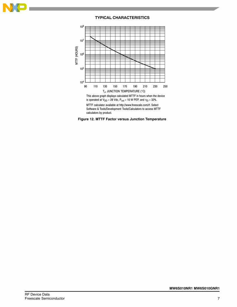
Figure 12. MTTF Factor versus Junction Temperature
250
108
90
TJ, JUNCTION TEMPERATURE (°C)
This above graph displays calculated MTTF in hours when the device
is operated at VDD = 28 Vdc, Pout = 10 W PEP, and ηD = 32%.
MTTF calculator available at http://www.freescale.com/rf. Select
Software & Tools/Development Tools/Calculators to access MTTF
calculators by product.
106
105
104
110 130 150 170 190
MT
TF
(H
OU
RS
)
210 230
107

8RF Device Data
Freescale Semiconductor
MW6S010NR1 MW6S010GNR1
fMHz
ZsourceΩ
ZloadΩ
800
820
840
3.1 + j1.9
2.7 + j2.2
2.8 + j1.7
10.1 + j2.3
8.3 + j2.5
8.2 + j3.3
VDD = 28 Vdc, IDQ = 125 mA, Pout = 10 W PEP
860
880
900
3.1 + j3.4
2.9 + j3.7
3.3 + j3.8
9.8 + j4.8
10.6 + j5.6
9.5 + j5.5
920
940
960
2.8 + j4.4
3.2 + j4.9
3.0 + j4.7
10.1 + j5.9
11.0 + j6.4
11.8 + j6.6
980 3.6 + j5.2 12.1 + j7.1
Figure 13. Series Equivalent Source and Load Impedance � 900 MHz
Zsource = Test circuit impedance as measured from gate to ground.
Zload = Test circuit impedance as measured from drain to ground.
Zsource
Zload
Input
Matching
Network
Device
Under
Test
Output
Matching
Network
f = 800 MHz
f = 980 MHz
Zo = 25 Ω
f = 800 MHz
f = 980 MHz
Zload
Zsource

MW6S010NR1 MW6S010GNR1
9RF Device DataFreescale Semiconductor
Figure 14. MW6S010NR1(GNR1) Test Circuit Schematic � 450 MHz
C5
C2
+
RF
OUTPUT
C6
VBIAS
VSUPPLY
RF
INPUT Z1
C9
Z5
R6
DUT
B2
C4
Z6
L1
C12 C11C10
Z5 0.475″ x 0.330″ MicrostripZ6 0.475″ x 0.325″ MicrostripZ8 1.250″ x 0.080″ MicrostripPCB Rogers ULTRALAM 2000, 0.030″, εr = 2.55
Z1 0.540″ x 0.080″ MicrostripZ2 0.365″ x 0.080″ MicrostripZ3 0.225″ x 0.080″ MicrostripZ4, Z7 0.440″ x 0.080″ Microstrip
C7
Z2
C8
Z3 Z4
C3
C1
+
R2R5
R1T1
R3
R4
T2
Z8Z7
B1
C13 C14 C15
+
Table 7. MW6S010NR1(GNR1) Test Circuit Component Designations and Values � 450 MHz
Part Description Part Number Manufacturer
B1, B2 Ferrite Bead 2743019447 Fair -Rite
C1 1 μF, 35 V Tantalum Capacitor T491C105K050AT Kemet
C2, C15 22 μF, 35 V Tantalum Capacitors T491X226K035AT Kemet
C3, C14 0.1 μF Chip Capacitors C1210C104K5RAC Kemet
C4, C9, C10, C13 330 pF Chip Capacitors ATC700A331JT150XT ATC
C5 4.3 pF Chip Capacitor ATC100B4R3JT500XT ATC
C6, C11 0.6-8.0 pF Variable Capacitors 27291SL Johanson
C7, C8, C12 4.7 pF Chip Capacitors ATC100B4R7JT500XT ATC
L1 39 μH Chip Inductor ISC-1210 Vishay
R1 10 Ω Chip Resistor CRCW080510R0FKEA Vishay
R2 1 kΩ Chip Resistor CRCW08051001FKEA Vishay
R3 1.2 kΩ Chip Resistor CRCW08051201FKEA Vishay
R4 2.2 kΩ Chip Resistor CRCW08052201FKEA Vishay
R5 5 kΩ Potentiometer 1224W Bourns
R6 1 kΩ Chip Resistor CRCW12061001FKEA Vishay
T1 5 Volt Regulator, Micro 8 LP2951CDMR2G On Semiconductor
T2 NPN Transistor, SOT-23 BC847ALT1G On Semiconductor

10RF Device Data
Freescale Semiconductor
MW6S010NR1 MW6S010GNR1
Figure 15. MW6S010NR1(GNR1) Test Circuit Component Layout � 450 MHz
MW6S010N 450 MHz
C5
C10
C6C7 C8
C9 R6
C4
C2C3
B1
R5
C1R2 R1
R3
R4
T1
T2B2
C14
C13
C15
L1
C12
C11

MW6S010NR1 MW6S010GNR1
11RF Device DataFreescale Semiconductor
TYPICAL CHARACTERISTICS � 450 MHz
IRL,
IN
PU
T R
ET
UR
N L
OS
S (
dB)
AC
PR
(dB
c), A
LT1
(dB
c)
500400
IRL
Gps
ACPR
f, FREQUENCY (MHz)
Figure 16. 2-Carrier W-CDMA Broadband Performance @ Pout = 3 Watts Avg.
−21
−6
−9
−12
−15
VDD = 28 Vdc, Pout = 3 W (Avg.), IDQ = 150 mA2−Carrier W−CDMA, 10 MHz Carrier Spacing, 3.84 MHz Channel Bandwidth, PAR = 8.5 dB @ 0.01% Probability (CCDF)
18.4
20.4
−65
37
34
31
28
−40
−45
−50
−55
η D,
DR
AIN
EF
FIC
IEN
CY
(%
)
ηD
Gps
, PO
WE
R G
AIN
(dB
)
25
−60 −18
20.2
20
19.8
19.6
19.4
19.2
19
18.8
18.6
410 420 430 440 450 460 470 480 490
ALT1
IRL
f, FREQUENCY (MHz)
Figure 17. 2-Carrier W-CDMA Broadband Performance @ Pout = 7.5 Watts Avg.
ηD
−50
IRL,
IN
PU
T R
ET
UR
N L
OS
S (
dB)
AC
PR
(dB
c), A
LT1
(dB
c)500400
−14
−4
−6
−8
−10
16.5
19
−55
55
50
45
40
−30
−35
−40
−45
η D,
DR
AIN
EF
FIC
IEN
CY
(%
)
Gps
, PO
WE
R G
AIN
(dB
)
35
−12
18.8
18.5
18.3
18
17.8
17.5
17.3
17
16.8
410 420 430 440 450 460 470 480 490
S11
f, FREQUENCY (MHz)
Figure 18. Broadband Frequency Response
VDD = 28 VdcPout = 10 WIDQ = 150 mA
65050
5
30
−25
0
−5
−15
−20
S11
S21
−10
25
20
15
10
100 150 200 250 300 350 400 450 500
S21
550 600
VDD = 28 Vdc, Pout = 7.5 W (Avg.), IDQ = 150 mA2−Carrier W−CDMA, 10 MHz Carrier Spacing, 3.84 MHz Channel Bandwidth, PAR = 8.5 dB @ 0.01% Probability (CCDF)
ALT1
ACPR
Gps
Figure 19. Single-Carrier N-CDMA ACPR, ALT1and ALT2 versus Output Power
−80
Pout, OUTPUT POWER (WATTS) AVG.
−10
−20
−30
−40
−70
0.1 1 10
−50
ACPR
VDD = 28 Vdc, IDQ = 150 mA,
f = 450 MHz, N−CDMA IS−95 Pilot,
Sync, Paging, Traffic Codes 8
Through 13
ALT
1 &
ALT
2, C
HA
NN
EL
PO
WE
R (
dBc)
AC
PR
, A
DJA
CE
NT
CH
AN
NE
L P
OW
ER
RA
TIO
(dB
c)
−60ALT2
ALT1

12RF Device Data
Freescale Semiconductor
MW6S010NR1 MW6S010GNR1
fMHz
ZsourceΩ
ZloadΩ
400
420
440
9.0 + j3.8
9.6 + j6.6
8.8 + j5.4
15.0 + j1.4
14.3 + j3.3
15.0 + j4.7
VDD = 28 Vdc, IDQ = 150 mA, Pout = 10 W PEP
460
480
500
10.6 + j9.5
11.5 + j13.9
10.7 + j12.6
16.3 + j7.3
16.4 + j11.1
16.9 + j12.7
Figure 20. Series Equivalent Source and Load Impedance � 450 MHz
Zsource = Test circuit impedance as measured from gate to ground.
Zload = Test circuit impedance as measured from drain to ground.
Zsource
Zload
Input
Matching
Network
Device
Under
Test
Output
Matching
Network
f = 400 MHz
Zo = 25 Ω
Zload
Zsource
f = 500 MHz
f = 400 MHz
f = 500 MHz

MW6S010NR1 MW6S010GNR1
13RF Device DataFreescale Semiconductor
PACKAGE DIMENSIONS

14RF Device Data
Freescale Semiconductor
MW6S010NR1 MW6S010GNR1

MW6S010NR1 MW6S010GNR1
15RF Device DataFreescale Semiconductor

16RF Device Data
Freescale Semiconductor
MW6S010NR1 MW6S010GNR1

MW6S010NR1 MW6S010GNR1
17RF Device DataFreescale Semiconductor

18RF Device Data
Freescale Semiconductor
MW6S010NR1 MW6S010GNR1

MW6S010NR1 MW6S010GNR1
19RF Device DataFreescale Semiconductor
PRODUCT DOCUMENTATION, TOOLS AND SOFTWARE
Refer to the following documents to aid your design process.
Application Notes
• AN1907: Solder Reflow Attach Method for High Power RF Devices in Plastic Packages
• AN1949: Mounting Method for the MHVIC910HR2 (PFP-16) and Similar Surface Mount Packages
• AN1955: Thermal Measurement Methodology of RF Power Amplifiers
• AN3789: Clamping of High Power RF Transistors and RFICs in Over-Molded Plastic Packages
Engineering Bulletins• EB212: Using Data Sheet Impedances for RF LDMOS Devices
Software• Electromigration MTTF Calculator
• RF High Power Model
For Software and Tools, do a Part Number search at http://www.freescale.com, and select the �Part Number� link. Go to theSoftware & Tools tab on the part�s Product Summary page to download the respective tool.
REVISION HISTORY
The following table summarizes revisions to this document.
Revision Date Description
4 Dec. 2008 • Changed Storage Temperature Range in Max Ratings table from -65 to +175 to -65 to +150 forstandardization across products, p. 1
• Removed Total Device Dissipation from Max Ratings table as data was redundant (information alreadyprovided in Thermal Characteristics table), p. 1
• Added Case Operating Temperature limit to the Maximum Ratings table and set limit to 150°C, p. 1
• Operating Junction Temperature increased from 200°C to 225°C in Maximum Ratings table, related�Continuous use at maximum temperature will affect MTTF� footnote added and changed 200°C to 225°C inCapable Plastic Package bullet, p. 1
• Corrected VDS to VDD in the RF test condition voltage callout for VGS(Q) and added �Measured in FunctionalTest�, On Characteristics table, p. 2
• Corrected Ciss test condition to indicate AC stimulus on the VGS connection versus the VDS connection,Dynamic Characteristics table, p. 2
• Updated Part Numbers in Tables 6, 7, Component Designations and Values, to RoHS compliant partnumbers, p. 3, 9
• Removed lower voltage tests from Fig. 10, Power Gain versus Output Power, due to fixed tuned fixturelimitations, p. 6
• Replaced Fig. 12, MTTF versus Junction Temperature with updated graph. Removed Amps2 and listedoperating characteristics and location of MTTF calculator for device, p. 7
• Replaced Case Outline 1265-08 with 1265-09, Issue K, p. 1, 13-15. Corrected cross hatch pattern inbottom view and changed its dimensions (D2 and E3) to minimum value on source contact (D2 changedfrom Min-Max .290-.320 to .290 Min; E3 changed from Min-Max .150-.180 to .150 Min). Added JEDECStandard Package Number.
• Replaced Case Outline 1265A-02 with 1265A-03, Issue C, p. 1, 16-18. Corrected cross hatch pattern andits dimensions (D2 and E2) on source contact (D2 changed from Min-Max .290-.320 to .290 Min; E3changed from Min-Max .150-.180 to .150 Min). Added pin numbers. Corrected mm dimension L forgull -wing foot from 4.90-5.06 Min-Max to 0.46-0.61 Min-Max. Added JEDEC Standard Package Number.
• Added Product Documentation and Revision History, p. 19
5 June 2009 • Modified data sheet to reflect MSL rating change from 1 to 3 as a result of the standardization of packingprocess as described in Product and Process Change Notification number, PCN13516, p. 2
• Added AN3789, Clamping of High Power RF Transistors and RFICs in Over-Molded Plastic Packages toProduct Documentation, Application Notes, p. 19
• Added Electromigration MTTF Calculator and RF High Power Model availability to Product Software, p. 19

20RF Device Data
Freescale Semiconductor
MW6S010NR1 MW6S010GNR1
Information in this document is provided solely to enable system and softwareimplementers to use Freescale Semiconductor products. There are no express orimplied copyright licenses granted hereunder to design or fabricate any integratedcircuits or integrated circuits based on the information in this document.
Freescale Semiconductor reserves the right to make changes without further notice toany products herein. Freescale Semiconductor makes no warranty, representation orguarantee regarding the suitability of its products for any particular purpose, nor doesFreescale Semiconductor assume any liability arising out of the application or use ofany product or circuit, and specifically disclaims any and all liability, including withoutlimitation consequential or incidental damages. �Typical� parameters that may beprovided in Freescale Semiconductor data sheets and/or specifications can and dovary in different applications and actual performance may vary over time. All operatingparameters, including �Typicals�, must be validated for each customer application bycustomer�s technical experts. Freescale Semiconductor does not convey any licenseunder its patent rights nor the rights of others. Freescale Semiconductor products arenot designed, intended, or authorized for use as components in systems intended forsurgical implant into the body, or other applications intended to support or sustain life,or for any other application in which the failure of the Freescale Semiconductor productcould create a situation where personal injury or death may occur. Should Buyerpurchase or use Freescale Semiconductor products for any such unintended orunauthorized application, Buyer shall indemnify and hold Freescale Semiconductorand its officers, employees, subsidiaries, affiliates, and distributors harmless against allclaims, costs, damages, and expenses, and reasonable attorney fees arising out of,directly or indirectly, any claim of personal injury or death associated with suchunintended or unauthorized use, even if such claim alleges that FreescaleSemiconductor was negligent regarding the design or manufacture of the part.
Freescale� and the Freescale logo are trademarks of Freescale Semiconductor, Inc.All other product or service names are the property of their respective owners.© Freescale Semiconductor, Inc. 2005-2006, 2008-2009. All rights reserved.
How to Reach Us:
Home Page:www.freescale.com
Web Support:http://www.freescale.com/support
USA/Europe or Locations Not Listed:Freescale Semiconductor, Inc.Technical Information Center, EL5162100 East Elliot RoadTempe, Arizona 852841-800-521-6274 or +1-480-768-2130www.freescale.com/support
Europe, Middle East, and Africa:Freescale Halbleiter Deutschland GmbHTechnical Information CenterSchatzbogen 781829 Muenchen, Germany+44 1296 380 456 (English)+46 8 52200080 (English)+49 89 92103 559 (German)+33 1 69 35 48 48 (French)www.freescale.com/support
Japan:Freescale Semiconductor Japan Ltd.HeadquartersARCO Tower 15F1-8-1, Shimo-Meguro, Meguro-ku,Tokyo 153-0064Japan0120 191014 or +81 3 5437 [email protected]
Asia/Pacific:Freescale Semiconductor China Ltd.Exchange Building 23FNo. 118 Jianguo RoadChaoyang DistrictBeijing 100022 China +86 10 5879 [email protected]
For Literature Requests Only:Freescale Semiconductor Literature Distribution Center1-800-441-2447 or +1-303-675-2140Fax: [email protected]
Document Number: MW6S010NRev. 5, 6/2009

Mouser Electronics
Authorized Distributor
Click to View Pricing, Inventory, Delivery & Lifecycle Information: NXP:
MW6S010GNR1 MW6S010NR1