document resume ed 190 901 title military … · 2014-02-18 · title military curricula for...
TRANSCRIPT

-----
DOCUMENT RESUME
ED 190 901 CE 026 586
TITLE Military Curricula for Vocational & TechnicalEducation, Basic Electronics School. CANTR;.0A-100-0010. Modules 23-25: Multivibrators,Waveshaping Circuits, Special Devices, ProgressCheCk.
7NST/TUTION Chief of Naval Education and Training Support,Pensacola, Fla,: Ohio State Univ., Columbus. NationalCenter for Research in Vocational Education.
PUP DATE Mar 77NOTE 121p.: For related documents see CE 026 560-593.
EDFS PRICE MF01/PC05 Plus Postage.DESCSIPTOFS Educational Experiments: *Electric Circuits:
*Electricity: *Electronics: IndividualizedInstruction: Learning Modules: PostsecondaryEducation: Programed Instruction; *StudentEvaluation: *Technical Education
IDENTIFIERS Military Curriculum Proiect: *Multivibrators(Electrical Equipment)
ABSTRACTThis document contains student progress checks
designed for use with individualized modules 23 through 25 in themilitary-developed course on basic electricity and electronics. Thecourse is one of a number of military-developed curriculum packagesselected for adaptation to vocational instructional and curriculumdevelopment in a civilian setting. One experiment and one progresscheck is provided for each lesson in the modules, Answers areincluded tt the ccnclusion of each module. (LRA)
************************************************************************ Reproductions supplied by EDRS are the best that can be made *
* from the or document, ************************************************************************

*1.eAjew,kelik
iT ACVA).-
ktrxs. in_
.
4
. -a
iM
CHIEF OF NAVAL EDUAT ION AND TRAINING
MARCH 1977
I
U S. DEPARTMENT OF HEALTH.EDUCATION s wiLF Apts.NATIONAL INSTITUTE
souc AT ION
THIS DOCUMENT HAS BEEN REPRO.DUCEO EXACTLY AS RECEIVED FROM
THE PERSON OR ORGANIZATION ORIGIN.MING IT POINTS OF VIEW OR OPINIONSSTATED DO NOT NECESSARILY REPRESENT OFFICIAL NATIONAL INSTITUTE OFEDUCATION POSITION OR POLICY
';
. , ..: , i.
- i,
ilitary urr. ... r ,s. 1
',.--' t. , .
$.2
for Vocational &Technical EducatioriT
BASIC ELECTRONICS SCHOOL.
MODULES 23 - 25. MULT IV IBRATORS ,
WAVESHAPING CIRCUITS, SPECIALDEVICES.
PROGRESS CHECKS.
THE NATIONAL CENTER
FOR RESEARCH IN VOCATIONAL EDUCATIONTHE OHIO STATE UNIVERSITY
2. ; :;-. 1-14r-terPtroklas....----,

MILITARY CURRICULUM MATERIALS
The military-developed curriculum materials in this coursepackage were selected by the National Center for Research inVocational Education Military Curriculum Project for dissem-ination to the six regional Curriculum Coordination Centers andother instructional materials agencies. The purpose ofdisseminating these courses was to make curriculum materialsdeveloped by the military more accessible to vocationaleducators in the civilian setting.
The course materials were acquired, evaluated by projectstaff and practitioners in the field, and prepared fordissemination. Materials which were specific to the nilitarywere deleted, copyrighted materials were either omitted or appro-val for their use was obtained. These course packages containcurriculum resource materials which can be adapted to supportvocational instruction and curriculum development.

...
#
e
MilitaryCurriculum MaterialsDissemination is .. .Lidriirrbra.....1arararbi
an activity to increase the accessibility ofmilitary-developed curriculum materials tovocational and technical educators.
This project, funded by the U.S. Office ofEducation, includes the identification andacquisition of curriculum materials in printform .from the Coast Guard, Air Force,Army, Marine Corps and Navy.
Access to military curriculum materials isprovided through a "Joint Memorandum ofUnderstanding!' between the U.S. Office ofEduc ion and the Department of Defense.t
The cquired materials are reviewed by staffand Abject matter specialists, and coursesdeemed applicable to vocational and tech-nical education are selected for dissemination.
The National Center for Research inVocational Education is the U.S. Office ofEducation's desitrated representative toacquire the materials and conduct the projectactivities.
Project Staff:
Wesley E. Budke, Ph.D., DirectorNational Center Clearinghouse
Shirley A. Chase, Ph.D.Project Director
JOU- 4
What MaterialsAre Available?
Le..i.:--.14......s...:..iai....s.;......L..-ig...ii.Lj
One hundred twenty courses on microfiche(thirteen in paper form) and descriptions ofeach have been piovided to the vocationalCurriculum Coordination Centers and otherinstructional materials agencies for dissemination.
Course materials include programmedinstruction, curriculum outlines, instructor&ides, student workbooks and technicalmanuals. Q
..,,
The 120 courses represent the followingsixteen vocational subject areas:
AgricultureAviationBuilding &
ConstructionTrades
ClericalOccupations
CommunicationsDraftingElectronicsEngine Mechanics
Food ServiceHealthHeating & AirConditioning
Machine ShepManagement &
SupervisionMeteorology &
NavigationPhotographyPublic Service
The number of courses and the subject areasrepresented will expand as additional materials with application to vocational andtechnical education are identified and selectedfor dissemination.
How Can TheseMaterials Be Obtained?
Contact the Curriculum Coordination Centerin your region for information on obtainingmaterials (e.g., availability and cost). Theywill respond to your request directly or referyou to an instructional materials agencycloser to you.
CURRICULUM COORDINATION CEIfrE BS
EAST CENTRALRebecca S. DouglassDirector100 North First StreetSpringfield, IL 62777217/782-0759
MIDWESTRobert PattonDirector1515 West Sixth Ave.Stillwater, OK 74704405/377.2000
NORTHEASTJoseph,F. Kelly, Ph.D.Director,225 West State StreetTrenton, NJ 08625609/2924562
NORTHWESTWilliam DanielsDirectorBuilding 17Airdustrial ParkDlympia, WA 98504206/753.0879
SOUTHEASTJames F. Shill, Ph.D.DirectorMississippi State UniversityDrawer DX
Mississippi State, MS 39762601/325.2510
WESTERNLawrence F. H. Zane, Ph.D.Director1176 University Ave.Honolulu, HI 96822808/948.7834

6
The National CenterMission Statementr ,/^.. !.../... ,.....,...n
The National Center for Research inVocational Education's mission is to increasethe ability of diverse agencies, institutions,and organizations to solve educational prob-lems relating to individual career planning,preparation, and progression. The NationalCenter fulfills its mission by
Generating knowledge through research
Developing educational programs andproducts
Evaluating individual program needsand outcomes
installing educational programs andproducts
Operating information systems andservices
Conducting leadership development andtraining programs
FOR FURTHER INFORMATION ABOUTMilitary Curriculum Materials
WRITE OR CALL.Program information OfficeThe National Cento for Research in Vocational
EducationThe Ohio State University960 Kenny Road, Columbus, Ohio 43210Telephone: 6141486.3655 or Toll Free 800/
848-4815 within the continental U.S.(except Ohio)
n
Military CUrriculumMateri,ls for
Vocational and\Technical Education
tor-7.111-k-1 ;-irl FieldF-!,.:rxr. Diviriion
Thr: I in'iCr-1. CrTilf.'T for nr f..4.nrchfrt ",.*c7.-,Iir-n:-I CrICntiOn
v

4
e
MODULES
TWENTY THREE
MULTIVIBRATORS
TWENTY FOUR
'WAVE SHAPING CIRCUITS
NTY FIVE
SPECIAL DEVICES
PROGRESS CHECK BOOKLET
1
t) 8

4
MODULE TWENTY THREE
IITLTIVIBRATORS
PROGRESS CHECK BOOKLET
3
9

-1
EXP. Twenty Three-1.0/ ,
. EXPERIMENTLESSON 1
Bistable Multivibrator. .("
The operation of a bistable multivibrator will be demontra!pby,performing,the steps outlined inthis Experiment. ,
Using an oscilloscope, you will observe-the change in state ofthe 11" and "0" outputs of the multivibrator when the proper input isapplied.
EQUIPMENT REQUIRED
OscilloscopeDevice 6F16 with template1X probe (three required)
IIG11 bistable multivibrator
PROCEDURE
1. Using all applicable safety precautionsi energize the oscillo-scope, obtain a line trace, and make the following settings:
a. CHANNEL SELECT to "Chopped".b. SENSITIVITY CONTROL (both channels) 5 volts/centimeter.c. SWEEP T1ME to .5 millisec/centimeter.d. Tr7b.c. to "D.C." (both channels). -e. Set channel "A" line trace 2 centimeters above center line.
Set channel "B" line trace 1 centimeter below center line.f. Connect 1X probes to channel "A" and "B" inputs.
11. Using all applicable safety precautions, set up Device 6F16, asfollows:
1r
a. Set up 6F16 using Template NG (Flip Flop multivibrator) andthe parts called for by the template.
b: Connect one end of a jumper to 4 volts (+ volt "battery"jack or the bottom of R3 or R6) leave the other end loose.
c. Connect channel "A" probe to-the 'l" output (Ql collector).:d. Connect channel 1B" probe to the "0" output (Q2.collector).e. Energize the 6F16 using the line%cord.
111. Now you are ready to gbserve the operation of the multivibrator.
1. What is the DC voltage level at the '11" output? VDC
2. What is the DC voltage level at the "0" output? VDC
3. Which transistor is conducting? ,
10
4

EXP. Twenty Three-I
4. The initial state of the muitivibrator is determined by
S. Using the free end of the jumper (+4 volt source) momentarilytouch the anode of CR 1. Did the flip-flop change state?
6. Momentarily apply +4 volts to the anode of CR 2. Did the flip-flop change state?
7. What conduction state are the transistors in now? Ql
Q2
8. Touch the jumper to the anode of CR 2 again. Did the flip-flopchange state?
9. Touch the jumper to the ano4 of CR 1. Did the flip-flop change,
state?
10. What conduction states are the transistors in now? Q1
Q2
IV. The following procedure will demonstrate the flip-flop actionwith a series of pulses applied to the circuit.
1. Remove the jumper from the +4 volt source.
2. Connect a third 1X probe to J2 on the Test Output Box locatedon the top of the Carrel. Connect the other end of the 1X probeto the shorting strap that is connected between Cl and C2. Younow have a 1KHz square wave input applied to Cl and C2. Cl - CR1and C2 - CR2 are used in this'circuit to shape the square wareinput into positive triggers that are applied to the base of eachof the transistors..
transistors3. Observe the outputs at the'coilectors of the two transistors antidraw the observed waveforms in the graticule below.
0 yr

EXP. Twenty-Three-I
4. Disconnect the probe from the "0" output (oscilloscope channel "B")and reconnect it to the shorting strip between Cl and C2. Set "B"channel SENSITIVITY to 20 v/cm. The "B" channel of the oscilio-'scope will now display the input signal.
S. Draw the waveforms displayed on the oscilloscope in the space below.
6. What is the frequency relationship between the input (Channel "B")and the output (Channel "A")?
CHECK YOUR RESPONSES WITH THEBOOKLET. WHEN YOUR RESPONSESLESSON II PROGRESS CHECK.IF YOUR RESPONSES DIFFER FROMAND PROCEDURES. IF YOU STILLSUPERVISOR.
1 ,
ANSWERS PROVIDED IN THE BACK OF THISAGREE WITH THE ANSWERS, PROCEED TO
THOSE GIVEN, RECHECK.YOUR SETTINGSHAVE A PROBLEM, SEE YOUR LEARNING

P.C. Twenty Three-I
PROGRESS CHECKLESSON I
Bistable Multivibrators
1. The bistable (flip-flop) multivibrator as stable states.
Bistable (flip-flops) multivibrators act like two-position elec-tronic
0
3. The flip-flop (bistable) multivibrator will/will not change stateswhen an external trigger of the correct amplitude is applied atthe proper input,
4. The flip-flop (bistable) multivibrator has two inputs andoutput(s).
S. In a flip-flop multivibrator, when one transistor is saturated, the:other transistor must be
6. In the circuit illustrated, which voltage divider network suppliesthe bias potential to the base of Ql?
7. To change the state of a flip-flop multivibrator (illustrated inquestion #6), a positive/negative pulse may be applied to the baseof the saturated transistor.

P.C. Twenty Three-I
8. Which of the below illustrated symbols most correctly depictsa flip-flop (tastable) multivibrator?
A. B.O
C. D.
0
9. Draw the "1" output waveform of the illustrated diagram. (The
"1" output is zero prior to to. The "1" state is a positivevoltage.)
4
1
s 1
TO T1
4
T21
T3
-Isc o
8

'P.C. Twenty Three-I
10. Label the inputs and outputs of the flip-flop multivibratorillustrated below.
-Vcc
11. To change the state of a flip-flop, a pulse is normally appliedto the transistor.
12. An input pulse of the correct polarity which changes the state of aflip-flop is called a/an pulse.
13. A trigger applied to the SET input which causes the "1" output VIgo positive or negative, ;III at the same time cause the "0" out-put to equal volts.
14. Define set state.
15. Define clear state.
9
1.5

P.C. Twenty Three-I
16. Identify the state of the flip-flop in each illustrated blockdiagrams.
A.+
F,Fovoit.0
B.
17. Identify each lead on the illustrated block diagram.
18. EVERY time a pulse is applied to theflip-flop will change states.
19. Assuming that the flip-flop is in the set state at to, draw
the "0" output waveform with the inputs as shown.(Assume the "1" state is a positive voltage.)
input, the
I t I
4 S
TC
To 11 112 113 14 1'5 T6
6
10
O
110 T1
I
I
a
1
I
112 T3
8
I
I
I
I
I
T4
II
I
I
8
I1
I
15
1
I
II!I
16
6

P.C. Twenty Three-I
THE ILLUSTRATION BELOW WILL BE USED TO ANSWER QUESTIONS 20-22.
20. In the above illustration, if QI is saturated, Q2 isand will be the most negative output.
a. saturated, Bb. saturated, Cc. cut off, Ad. cut off, B
21. In the above illustration, with Ql saturated, a pulseapplied to will cause QI to cut off.
a. positive, Cb. negative,Cc. positive, Dd. negative, B
22. In the illustration above, QI is saturated. If a negative pulseis applied to C, what will happen?
a.- Q2 will become saturated.b. Q2 will become cut off.c. QI will cut off.d. Nothing will happen. 16
..- -......--.----.^.-
_..-- - -----
P.C. Twenty Three-I
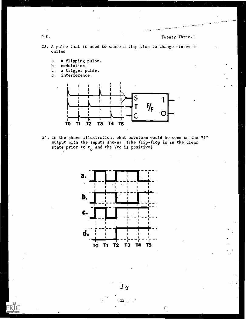
23. A pulse that is used to cause a flip-flop to change states iscalled
a. a flipping pulse,b. modulation.c. a trigger pulse.d. interference.
24. In the above illustration, what waveform would be seen on theoutput with the inputs shown? (The flip-flop is in the clearstate prior to to and the Vcc is positive)
TO T1 T2 13 14 TI5
1.2
I-'

P.C.;Agent) Three-I
25. If a flip-flop is in the set state, a trigger on theinput will change it to the clear state. (Use the most complete correctanswer.)
a. set, clear, or toggleb. set or togglec. clear onlyd. toggle or cleare. toggle only
ON QUESTIONS 26 AND 27 MATCH THE INPUTS SHOWN WITH THE CORRECT "1" OUT-PUT WAVEFORM. (The flip-flop is in the clear state prior to to and Vccis positive.)
26.
TO 11 T2 T3
S
T Fif0C
_I
I .. FiF .J I
f
11
1 0 11
1.... 1 1 : 1 1
1I 1
1
. TO TI 'T2 T3i
CHECK YOUR RESPONSES WITH THE ANSWERS PROVIDED IN THE BACK OF THISBOOKLET. WHEN YOUR RESPONSES AGREE WITH THE ANSWERS, PROCEED TOLESSON II OF THIS MODULE.
13
1.9

EXP. Twenty Three-II
EXPERIMENTLESSON II
Astable Multivibrator (Free Running)
The operation of an astable multivibrator will be demonstrated' byperforming the:steps outlined in this Experiment.
Using an oscilloscope, you will observe the output of an astablemultivibrator.
EQUIPMENT REQUIREDOscilloscopeDevice 61:16 with template "H" free running multivibrator1X probe
PROCEDURE:
Using all applicable safety precautions, energize the oscillo-scope, obtain a line trace, and make the following settings.
a. SWEEP TIME to .5 millisectnids/cm.b. CHANNEL SELECT to "Channel A".c. SENSITIVITY to 5 volts/cm.d. Connect the 1X probe to Channel "A" input.
II. Using all applicable safety precautions, set up Device 6F16 asfolldws:
a. Set up 6F16 using Template OH (Free Running Multivibrator)and the parts called for by the template.NOTE: DO NOT INSTALL RESISTOR R7.
b. Connect Channel "A" probe to the output.C. Energize the 6F16 using the line cord.
III. You are now ready to observe the operation of an astablemultivibrator.
1. Observe the output waveform and draw the observed waveform inthe space below. NOTE: If there is no output, the circuit isprobably balanced. T unbalance the circuit, momentarily insertR7 (390 ohm). Once the circuit is operating, R7 is not neces-sary; remove it.
d
1420

EXP. Twenty Three-II
2. How long is Q2 in conduction? (Measure the time of the conductinghalf cycle.)
3. How long is Q2 cut off?
Now yo(1 will set up the multivibrator for an asymmetric output."AsymMtric" means the output will not be symmetrical; that is,one transistor will conduct longer than the other. To accomplishthis, remove C2 (.033 pfd capacitor)and replace it with a :010 pfdcapacitor.
4. Set the SWEEP TIME on the oscilloscope to .2 millisec/cm and recordthe waveform displayed on the oscilloscope in the space below.
.Mma
I 14 H
S. What is the time of the conducting half cycle of Q2?
6. What is the time of the "cut off" half cycle of Q2?
CHECK YOUR RESPONSES WITH THE ANSWERS PROVIDED IN THE BACK OF THIS BOOK-LET. WHEN YOUR RESPONSES AGREE WITH THE ANSWERS, PROCEED TO kESSON IIPROGRESS CHECK.IF"YOUR RESPONSES DIFFER FROM THOSE GIVEN, RECHECK YOUR SETTINGS ANDPROCEDURES. IF YOU STILL HAVE A PROBLEM; SEE YOUR LEARNING SUPERVISOR.
15 2

P.C. Twenty Three-II
PROGRESS CHECKLESSON II
Astable Multivibrators
1. An astable multivibrator is also known as a/anmultivibrator.
2. The astable multivibrator operates like a square-vgve
3. The astable multivibrator has input trigger(s) andoutput(s).
USE THE BELOW ILLUSTRATION FOR QUESTIONS 4 THROI1GH 9.
4. In the figure above, which component(s) determine the amount oftime Q2 is in a cut-off state?
S. If Q2 is cut-off, Ql must be
6. The rate of charging of Cl depends on the time constant pro-duced by which componente
7. The length of time that transistor Ql remains cut off is determinedby the charging rate of capacitor
2216
3
P.C. Twenty Three-II
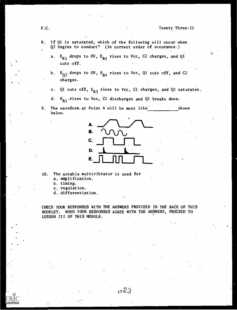
8. If Ql is saturated, which of the following will occur whenQ2 begins to conduct? (In correct order of occurance.)
a. ER1
drops to OV, ER4
rises to Vcc, C2 charges, and Ql
cuts off.
b. EQ2
drops to OV, ER4
rises to Vcc, Ql cuts off, and C2
charges.
c. Ql cuts off, ER3 rises to Vcc, Cl charges, and Q2 saturates.
d. ER1
,rises to Vcc, Cl discharges and Ql breaks down.
The waveform at Point A will be most like shownbelow.
A.
B.
10. The astable multivibrator is used fora. amplification.b. timing.c, regulation.d, differentiation.
CHECK YOUR RESPONSES WITH THE ANSWERS PROVIDED IN THE BACK OF THISBOOKLET, WHEN YOUR RESPONSES AGREE WITH THE ANSWERS, PROCEED TOLESSON III OF THIS MODULE,
1723

EXP.
EXPERIMENTLESSON III
Monostable Multivibrator (One Shot)
Twenty Three-III-1
The operation of the Monostable Multivibrator will be demonstratedby performing the steps outlined in this experiment.
Using an oscilloscope, you will observe the changes in. state of the"0" output of the multivibrator when the propbr input is applied.Since the "1" output is the inverse of the "0" output, it will not benecessary to look at the "1" output.
EQUIPMENT REQUIRED,
OscilloscopeDevice 6F16 with template #11X probe (three required)
PROCEDURE:
I. Using all' applicable safety precautions, energize the oscillo-scope and obtain a line trace. Make the following additionalsettings:
a. SWEEP TIME to .2 millisec/cm.b. SENSITIVITY CONTROL to 20 volts (Channel "A") and S volts
(Channel."B").c. CHANNEL SELECT to "Chopped" and obtain a line trace for
Channel "B".d. Connect 1X probes to channel "A" and "B" inputs.e. Set the VERTICAL POSITIONS as follows; Channel "A", +1 cm;
Channel "B", -1 cm.
II. Using all applicable safety precautions, set up Device 6F16 asfollows:
a. Set up 6F16 using Template #1 and the parts called forby the template. (Use a .01 of capacitor for Cl.)
b. Connect the channel "A" probe to the base of Q1 (rightside of C3).
c. Connect the channel "B" probe to the "0" output (Q2 Col-lector).
d. Energize the 6F16 using the line cord.
III. Connect a, 1X 'probe to J2 on the Test Signal Junction Box. Con-
nect the other end of this probe to the 6F16 input.
2418
EXP. Twenty Three-III-1
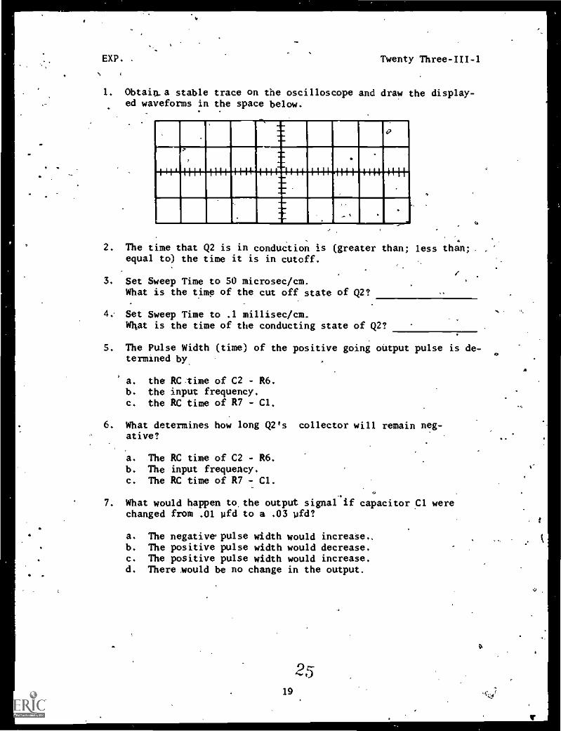
1. Obtain.a stable trace on the oscilloscope and draw the display-ed waveforms in the space below.
ICI' 111111 I I 111111111111 4414
2. The time that Q2 is in conduction is (greater than; less than;.equal to) the time it is in cutoff.
I3. Set Sweep Time to 50 microsec/cm.
What is the time of the cut off state of Q2?
4. Set Sweep Time to .1 millisec/cm.What is the time of the conducting state of Q2?
5. The Pulse Width (time) of the positive going output pulse is de-termined by
a. the RCtime of C2 - R6.b. the input frequency.c. the RC time of R7 - Cl.
6. What determines how long Q2's collector will remain neg-ative?
a. The RC time of C2 - R6.b. The input frequency.c. The RC time of R7 - Cl.
7. What would happen to, the output signal if capacitor C1 werechanged from .01 nfd to a .03 pfd?
a. The negative.pulse width would increase..b. The positive pulse width would decrease.c. The positive pulse width would increase.d. There would be no change in the output.
19
EXP. Twenty Three-III-1
8. Remove Cl (.01 ofd) and replace with a .03 ofd capacitor. What isthe pulse width of the negative pulse?
9. When you changed the capacitance of Cl, the positive pulse widthincreased; decreased; remained the same)
THIS CONCLUDES THE JOB SHEET ON MULTIVIBRATORS. SECURE THE TESTEQUIPMENT AND PUT ALL COMPONENTS BACK IN THEIR PROPER PLACES.IF YOUR RESPONSES DIFFER FROM THOSE GIVEN, RECHECK YOUR SETTINGSAND PROCEDURES. IF YOU STILL HAVE A PROBLEM, SEE YOUR LEARNINGSUPERVISOR. CHECK YOUR RESPONSES WITH THE ANSWERS PROVIDED IN THEBACK OF..THIS BOOKLET. WHEN YOUR RESPONSES AGREE WITH THE ANSWERS,PROCEED TO LESSON III PROGRESS CHECK,
20
a

I.S. Twenty Three-III
INFORMATION SHEETWAFER ROTARY SWITCHES
The wafer rotary'switch is usually several separate switches linkedganged) together. Figure 1 shows a typical wafer rotary switch.
,Notice the current path formed by the extended terminal, contact ring,wiper arm (part of the contact ring) and the short terminal touchingthe wiper arm.
I
Figure 1
On most schematic diagrams the wafer rotary switch is shown in one posi-tion only. You must mentally determine the current path through theswitch for any of the other positions. Figure 2 is a schematic repre-sentation of the wafer switch shown in Figure 1. The conduction pathfor the switch position shown is from terminal 1 through the contactring to terminal 4 If this switch were turned two positions counter-clockwise, the conduction path would now be'from terminal 1 through thecontact ring to terminal 2.
O
J
3
a 6057 6
Figure-12
21 27O

I=S. Twenty Three-IllA
Figure 3 shows the schematic symbol fora slightly different type ofwafer rotary switch. The basic construction of this switch is similarto the one in Figures 1 and 2. Note that the contact ring is split andthere isa wiper and an extended terminal for each of the contact ringsegments. There areactually Iwo switches mounted on one wafer. Eachswitch operates the'same as tilq.switch in Figures 1 and 2, but thereare fewer switch positions available. This switch in the position shownhas a conduction path from terminal 12 through one half of the split con-duction ring to terminal 11. ,There is also a conduction path from termin-al 6 to terminal 5 through the other half of the conduction ring. If
this switch were rotated two positions counterclockwise terminal 12 wouldbe connected to terminal '9 and termnal 6 would be connected to terminal
3.,
11
Figure 3
Figure 41shows what a typical wafer rotary switch might look like on aschematic drawing. When these switches are shown on a schematic drawing,usually only those sections and/or positions used are shown. If there ismore than one section shown for a switch, all the sections will be
' ,.switched at the same time. The switch positions will be labeled on theschematic so you can tell where the wiper u, the switch is actuallypositioned for a given switch position. For purposes of clarity on theschematic drawing, you may see an extra switch symbol with the switchpositions indicated around it.
Figure 4
?28
40
4.
Exp. Twenty Three-III-2
EXPERIMENTLESSON III
PART 2
Multivibrator Systems
This experiment will demonstrate the operation of a system utilizing allthree of the multivibrators that you have studied: astable, bistable andmonostaule. You will be using the NIDA 204 Function Generator for thisdemonstration. The NIDA 704 Function Generator is a complex lookingpiece of equipment, but don't let this frighten you; this experiment willcover only three of the PC boards and some of the front panel controls.
NOTE: Refer to information sheet Twenty Three-Ill that precedes thisexperiment for an explanation of wafer rotary switch operation.
SAFETY PRECAUTIONS: Observe all standard safety precautions. Do notenergize the NIDA 204 until directed to do so.
EQUIPMENT REQUIRED:
NIDA 204 Function GeneratorOscilloscopeflt Probe (2)
BNC BNC Coaxial Cable (2)BNC "Tee" Connector (1)
PROCEDURE:
PC 204-2 Printed Circuit CardPC 204-3 Printed Circuit CardPC 204-4 Printed Circuit CardInstruction Manual, NIOA 204
1. Energize and set up the oscilloscope for CHANNEL A operation and EX-TERNAL TRIGGER mode.
a. Using a BNC-BNC coaxial cable and the BNC "Tee" connector, connectthe oscilloscope CHANNEL A INPUT to the EXTERNAL TRIGGER INPUT.Connect a IX Probe to the BNC "Tee" connector.
2. Set the front panel controls of the NIDA 204 Function Generator asfollows:
a. TRIGGER switch to "EXT."b. FREQUENCY switch to "10 KHz. It
c. FREQUENCY dial to "1.5."d. INPUT controls - not used.e. PULSE WIDTH switch to "1 microsecond."f. PULSE WIDTH dial to' 8 ".
g. OUTPUT SYMMETRY - not used.h. OUTPUT LEVEL - fully clockwise.i. FUNCTION switch to 11-1_11. (square wave).
3. Remove the top cover of the NIDA 204.
23 29

Exp. Twenty Three-I11-2
4. Connect the CHANNEL A probe to PC 204-2, pin ID.
NOTE: DO NOT ENERGIZE THE NIDA 204.
5. Study Figure i , page 29/30 of this experiment, and answer...
(1) The CHANNEL A probe is connected to
a. the input to the astable multivibrator.b. the output of the monostabie muitivibrator.c. the input to the monostable multivibrator.d. the output of the astable multivibrator.
(2) FREQUENCY SWITCH S2 is shown in the 10 KHz position. Will theastable muitivibrator operate with the switch in this position?(Yes/No).
(3) The astable multivibrator wi;1 operate with switch S2 in
a. any position.b. any position except "i Hz."c. the "10 KHz" position only.d. any position except "10 KHz."
6. Plug in and energize the NIDA 204 Function Generator.
7. Check your answers to questions 5(2) and 5(3) by switching FREQUENCYSWITCH (S2) to its other positions and checking for a square waveoutput with the oscilloscope. If the results of this check agreewith your answers, continue to step 8. If your answers do notagree,go back to Figure 1 and study the action of the FREQUENCYSWITCH.
8. Ensure the FREQUENCYSWITCH.is in the "10 KHz" position. Determinethe period and compute the output frequency of the astable multi-vibrator. Record your results. Period Frequency
30
24

Exp. Twenty Three-III-2
9. Change the setting of the FREQUENCY DIAL (R21A and B) to "4" andanswer the following questions:
(1) The output frequency of the astable multivibrator
a. ,increased.b. decreased.c. remains the same.
(2) When you changed the setting of the FREQUENCY DIAL, you changedthe
a. capacitance of the RC circuit that determines the outputfrequency.
b. resistance of the RC circuit that determines the outputfrequency.
c. input frequency to the astable multivibrator.
10. The output of the astable multivibrator (PC204-2, pin 10) connectsto the input of the bistable multivibrator (PC204-3, pin 3). Thebistable multivibrator has two outputs: one at pin 8 and one at pin11. Using Figure 1 answer the following questions:
(1) The output frequency of the bistable multivibrator is determinedby the
a. RC time constants within the bistable multivibrator.b. setting of switch S3.c. input frequency to the bistable multivibrator.d. setting of R22 (PULSE WIDTH DIAL).
(2) The output frequency of the bistable multivibrator is (twice/the same as/one half) the input frequency.
Set up the oscilloscope for dual trace operation and connect theCHANNEL B INPUT to PC204-3, pin 8, with 1X probe. Check youranswer to 10 (2) with the oscilloscope.
(3) What is the, relationship between the bistable multivibratoroutputs (pins 8 and 11)?
a. The two outputs are identical.b. Pin 8 output is twice the frequency of pin 11 output.c. The outputs at pins 8 and 11 are equal in frequency but 180
degrees phase displaced.
11. Disconnect the CHANNEL A probe from PC204-2, pin 10, and reconnectit to PC 204-3, pin 11. Check your answer to 10 (3) with theoscilloscope.
25

Exp. Twenty Three-111-2
12. The third circuit used in this experiment is the monostable multi-vibrator (PC204-4). The components C1-4, CR1-4, CR2-4, R1-4 andR2-4 are not used. Pulse width switch (S3) and PULSE WIDTH DIAL(R22) are associated with the monostable multivibrator. Answer thefollowing questions using Figure 1:
(1) The monostable multivibrator will generate an output pulse eachtime the input
a. changes polarity.b. goes positive.c. goes negative.d. goes either positive or negative.
(2) The amount of time the monostable multivibrator will remain inits "unstable" state is determined.by the
a. RC time constant of the circuit.b. input to the circuit.
(3) The amount of time the monostable multivibrator will remain inits stable state is determined by the
a. RC time constant of the circuit.b. input to the circuit.
(4) With the PULSE WIQTH SWITCH (S3) in the "10 psec" position,capacitor is in (series/parallel) with capacitor C3-4.
a. C13b. C14c. C16d. C17
(5) With the PULSE WIDTH SWITCH (S3) in the "1 sec" position, whatcapacitor(s) determine the pulsewidth?
a. C17 and C3-4b. C15 and C3-4c. C3-4 onlyd. C13 and C3-4
(6) The PULSEWID1H DIAL (R22) will control the (capacitance/resistance)of the RC time constant in the monostable multivibrator.
13. Disconnect The CHANNEL 8 probe from PC204-3, pin 8, and reconnectit to PC204-4, pin 9. Go ahead and verify the answers to questionsin step 12 by checking the operation of the monostable multivibratoron your own.
a
32"-'26
4
Exp. Twenty Three-Ill-2
NOTE: At the frequencies used in this experiment, the monostablemultivibrator output will be unstable if the PULSE WIDTHSWITCH (S3) is set to any position other than "1 usec" or"10 usec." In the "10 usec" position, setting the PULSEWIDTH DIAL (R22), above "8" will probably result in unstableoperation. This will not harm the equipment, but the outputis unusable.
14. Before continuing with the experiment, let's review what you havelearned so far. First you learned that the astable multivibratorin the NIDA 204 will operate with the FREQUENCY SWITCH (S2) in the"10 KHz" position only, and that the frequency can be varied withthe FREQUENCY DIAL (R21A and B). The output of the astable multi-vibrator is the input signal to the bistable multivibrator.
The bistable multivibrator has two outputs that are 180 degrees phasedisplaced from each other. The output frequency of the bistablemultivibrator is one-half the input frequency. Only one of theoutputs from the bistable multivibrator is used in this experiment.This output is taken from PC204-3, pin 11, and is applied to theinput of the monostable multivibrator. The monostable multivibratorwill put out a pulse at the frequency of the input. This outputpulse will be of a duration determined by the setting of thePULSE WIDTH controls (S3 and R22).
15. Now, go to Figure 1 and look at the FUNCTION SWITCH (S4).
(1) With this switch in the position shown (square wave), where isthe signal,at the OUTPUT jack coming from (disregard the amplifier)?
a. PC 204-4, pin 12.b. PC 204-4, pin 9.c. PC 204-3, pin 11.d. PC 204-3, pin 8.
(2) Where will the signal at the OUTPUT jack come from if the FUNCTION' SWITCH (S4) is placed in the 14-L..." (pulse) position?
a. PC204-4, pin 12.b. PC204-4, pin 9.c. PC204-3, pin 11.d. PC204-3, pin 8.
16. Remove the oscilloscope probes from the NIDA 204'. Place the oscillo-scope in CHANNEL A mode and disconnect the 1X probe or CHANNEL A fromthe BNC "Tee" connector. Connect the OUTPUT jack of the NIDA 204 toCHANNEL A of the oscilloscope using a BNC BNC cable.
27

Exp. Twenty Three-111-2
17. Switch the FUNCTION switch back and forth between "pulse" and "squarewave" positions. Note that the output changes from a pulse to asquare wave.
(1) With the switch in the "pulse" position, the output signal istaming from
a. PC 204-2.b. PC 204,-3.
c. PC 204-4.
(2) With the switch in the "square wave" position, the output signalis coming
a. PC 204-2.b. PC 204-3.c. PC 204-4.
(3) If you had no output with the FUNCTION SWITCH (S4) in the "pulse"mode, but you had an output in the "square wave" mode, which ofthe following would be the most likely problem area?
a. Switch S2.b. PC204-3.c. 'PC204-4.d. Power supply.
Question 17(3) shows a troubleshooting aid that is effective on many typesof electronic equipment. Many times a casualty may be isolated to aspecific area or even a circuit by using switches on the equipment toswitch various sections in or out of operation. To use this aid requiresa schematic drawing, block diagram, or other source of information toshow what is happening when a certain switch is moved to a differentposition.
CHECK YOUR RESPONSES WITH THE ANSWERS PROVIDED IN THE BACK OF THIS BOOKLET.IF YOUR RESPONSES DIFFER FROM THOSE GIVEN, RECHECK YOUR SETTINGS AND ,
PROCEDURES. IF YOU STILL HAVE A PROBLEM, SEE YOUR LEARNING SUPERVISOR.WHEN YOUR RESPONSES AGREE WITH THE ANSWERS GIVEN AND YOU FEEL THAT YOUHAVE MASTERED THE MATERIAL IN THIS EXPERIMENT, REPLACE ALL THE COVERSAND RETURN YOUR 'EQUIPMENT TO ITS STOWAGE, THEN PROCEED TO THE PROGRESSCHECK.
3428

.36
90 MI4,0 101Iz
,i....-k.P00111
ONWQ 9,
S1C 101104
(,) Mt CIVOS$111Cry
-0111Ce is)
FICIIENCY
,
.
M44
PC 104-1 1STAIL1 In1110114101 PC 104.3 1104115 1101.11/1114I01,
111F-'PC 314.4 1100004111 MOITIVISIMI
I
S
4 R1-3
3
C1,39I (--13.3
C3.3
113
15-3
1311QP
(),..
nn0(5fl rU
SQUARE WAVE & PULSE MODE
Figure #1
011illi
36

P.C. Twenty Three-III
PROGRESS CHECKLESSON III
Monostable Multivibrators
1. The monostable multivibrator has input(s).
USE THE BELOW ILLUSTRATION FOR QUESTIONS AS INDICATED.
Lvcc
01
AO
2. Before a trigger is applied to the circuit in figure 1, Ql willbe (cutoff/saturated) and Q2 will be (cutoff/saturated).
3. To change the state of the circuit in figure 1, apulse would be applied at the input.
4. The monostable muliv'.brator returns to its stable state after a(definite/indefinite") period of time.
5. In figure 1, point A is the (input/output) and pointis the (input /output.)
6. In figure 1, when Ql is saturated the output wiii
3731

st
P.C. Twenty Three -Ill
In questions 7 and 8 match the input triggers shown with the outputwave forms. (Use the circuit represented. in Fig. 1)
7.
8.
To T1 T2 T3 14I to I I
F.4 i II I
TO T1 T2' T3 T4
9. Refer to figure 1. The time duration of the negative output pulseis determined by
a. C2 and R2.b. R1 and Cl.c. Cl and R2.
RI and C2.
Match the circuits following question 15 with their correct titles forquestions 10 through 15.
10. Flip-flop multivibrator
11. Monostable multivibrator'
12. Astable multivibrator
13. Bistable multivibrator
14. One-shot multivibrato.r
15. Free running multivibrator
3832

P.C.
a.
b.
C.
OUTPUT00.1
01
0
Twenty Three -III
9 vcc
OUTPUTNO.2
33 39
4;
P.C. -
16. When the circuit shown in figure C on the previous page is energized46
Twenty Three-III
a. Ql only will saturate.b. Q2 only will saturate.c. Ql or Q2 will saturate.d. 0 and Q2 will saturate.
17. When circa illustrated on the previous page is energized
a. Ql or Q2 wi's saturate and remain saturated.b. Ql will cut oc. Ql and Q2 will alternately saturate and cut off.d. a sawtooth waveform will appear on output 2.
18. When circuit A illustrated on the previous page is energized
a. Ql will saturate and remain saturated until triggered.b. Q2 will saturate and remain saturated until triggered.c. it is impossible to tell which transistor Will saturate first.d. neither Ql or Q2 will saturate.
CHECK YOUR RESPONSES WITH THE ANSWERS PROVIDED IN THE BACK OF THISBOOKLET. WHEN YOUR RESPONSES AGREE WITH THE ANSWERS, SEE YOURLEARNING SUPERVISOR FOR THE END OF MODULE TEST.
34

-
MODULE
TWENTY FOUR
WAVE SHAPING CIRCUITS
PROGRESS CHECK BOOKLET
35 41
a

EXP.t
Twenty Four-I-1
EXPERIMENTLESSON IPART 1
Clippers
;
Device 6F16 with templates "D" and "E" introduction to clippersOscilloscopeIX test probe (2)
SAFETY PRECAUTIONS: OBSERVE ALL APPLICABLE SAFETY PRECAUTIONS.
PROCEDURE:
I. Set up the oscilloscope for dual trace operation.
a. CHANNEL SELECT to "Chopped" and obtain line traces for bothchannels.
b. Set the VERTICAL POSITION channel "A" to (4) 1 cm andChannel B to (-) 1 cm.
c. Set trigger source to line.d. Set sweep time equal to 5 cosec /cm.e. .Set Channel A and B sensitivity equal to 10v/cm.f. Set Channel A and B AC/DC switches to "DC".
II. Set up device 6F16 as follows:
a. Use template D and the parts called for on this template.b. Energize the 6F16 using the line cord.
III. 1. Connect one of the test probes to channel "A" and theother one to channel "B". Connect the channel "A" probe tothe clipper circuit input. Observe and draw the inputwaveform.
;-4-1444+1++1-1444-44-14,
aft
How much peak-to-peak voltage is applied to the clippercircuit?
42
36
ti
EXP. Twenty Four-I-1
2. Now connect the channel "B" test probe to the clipper output.Observe and draw the output waveform.
1111 EMI1111111111111/11111111111111
1111111111111111111111111111IN EllWhat kind of clipper is this?
3. Secure the power (unplug the power cord - FROM THE WALL SOCKET -and reverse the diode. Before you energize thi device deter-mine what kind of clipper this is.Now, plug the line cord back In and draw the output waveform.
.
-4-
Were you right?
4. Okay, now let's add some bias. Secure the power again. Removethe shorting strip below the resistor. Plug one end of the redjumper patch cord into the hole right below the resistor and theother end into the negative side of the battery bias voltage.Re-energize the device and observe and draw the output waveform.
-AL
What kind of clipper is this?
37 43

EXP. Twenty Four-I-1
5. Plug the patch cord into the positive side of the battery biasvoltage. Observe and draw the output waveform.
:1H
=dim
H1-4 11 I
What kind of clipper is this?
6. Now Letts make some other kinds of clippers. All you have to dois reverse the diode again - SECURE THE POWER, FIRST!
Observe and draw the output waveform.
What kind of a clipper is this?
7. Go back to the negative side of the battery voltage. Observeand draw the output waveform.
1111 1111 1111 III+ 6 11 11 11 Hi! IIII 11H'
What kind of clipper is this?
44
38
EXP. Twenty Four-I-1
Part 2, PARALLEL CLIPPERS, is next. Secure the power to the 6F16,disconnect the test probes, remove the components and stow themwhere they belong, and return the template to its stowage.
If you wish, just for a few minutes, yawn, stretch, get a cup ofcoffer, or take a short break.
CHECK YOUR RESPONSES WITH THE ANSWERS PROVIDED IN THE BACK OF THISBOOKLET. WHEN YOUR RESPONSES AGREE W1TH THE ANSWERS, PROCEED TO PART2 OF THIS JOB SHEET.IF YOUR RESPONSES DIFFER FROM THOSE GIVEN, RECHECK YOUR SETTINGS ANDPROCEDURES. IF YOU STILL HAVE A PROBLEM, SEE YOUR LEARNING SUPERVISOR.
439 0

EXP.
EXPERIMENTLESSON IPART 2
Clippers
PROCEDURE:
Twenty Four-I-2
I. Time to search for templates again!a. Find template #E, Parallel Clippers, and put it on
the 6F16 (the same way as before.)
b. Locate the components and "plug 'em in."
Congratulations! You have built a parallel clipper.
t c. Use the oscilloscope set up as EXP. Twenty Four I-1.
d. Energize the 6F16 and look at the input waveform.Is it still the same as before?If not, see your learning supervisor.
II. 1. Now look at the output. Here we go again - observe anddraw the output waveform.
What kind of parallel clipper is this?
2a. Deenergize the 6F16.b. Reverse the diode.c. Reenergize the 6F16.-
What kind of parallel. clipper is this?
Observe and draw the output waveform.
1_1
J46-
40
EXP. Twenty Four-I-2
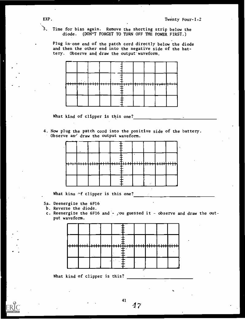
3. Time for bias again. Remove the shorting strip below thediode. (DON"T FORGET TO TURN OFF THE POWER FIRST.)
Plug inone end of the patch cord directly below the diodeand then the other end into the negative side of the bat-tery. Observe and draw the output' waveform.
-4
1111 lift 1111 Hit 4i irttil
What kind of clipper is this one?
4. Now plug the patch cord into the positive side of the battery.Observe an draw the output waveform.
'1'1' IiII 1111 fill
What kiwi ^f clipper is this one?
Sa. Deenergize the 6F16b. Reverse the diode.c. Reenergize the 6F16 and.- ,ou guessed it - observe and draw the out-
put waveform.
What kind of clipper is this?

EXP. Twenty Four-I-2
6. Now bring the patch cord back to the negative side of thebattery. What did you see? Draw it!
4-14+-144-44-1-1-444-4+
t I I
I 11 H
.1
.10M
How about this one? What is it?
This concludes the experiment on clippers.
CHECK YOUR RESPONSES WITH THE ANSWERS PROVIDED IN THE BACK OF THISBOOKLET. WHEN YOUR RESPONSES AGREE WITH THE ANSWERS, PROCEED TOLESSON I PROGRESS CHECK.IF YOUR RESPONSES DIFFER FROM THOSE GIVEN, RECHECK YOUR SETTINGS ANDPROCEDURES. IF YOU'STILL HAVE A PROBLEM, SEE YOUR LEARNING SUPER-VISOR.
46'
42
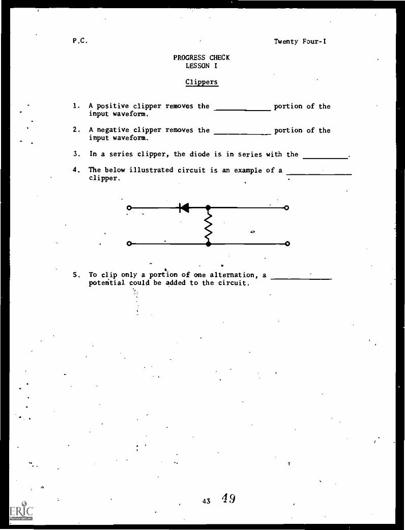
P.C. Twenty Four-I
PROGRESS CHECKLESSON I
Clippers
1. A positive clipper removes the portion of theinput waveform.
2. A negative clipper removes the portion of theinput waveform.
3. In a series clipper, the diode is in series with the
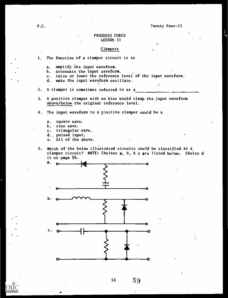
4. The below illustrated circuit is an example of aclipper.
0
47
-0
S. To clip only a portion of one alternation, apoteitial could be added to the circuit.
43 .4 9
0
P.C. Twenty Four-I
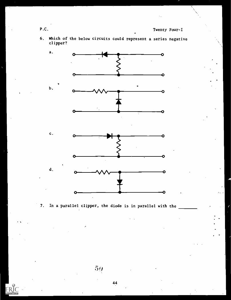
6. Which of the below circuits could represent a series negativeclipper?
a.
b.
c.
d.
0 0
0
I0
0
0
.
0
0
0
0
0
0
0
0 , -
7. In a parallel clipper, the diode is in parallel with the
5 0
44

P.C. Twenty Four-I
8. Match the below illustrated circuits with their correct titles.
a.
9
h.
O
O 0
d.
e.
0
1. series negative clipper with positive bias.2. parallel positive clipper with negative bias.3. parallel positive and negative clipper with positive and
negative bias.4. series positive clipper with positive bias.5. parallel negative clipper with positive bias.6. series negative clipper with negative bias.7. parallel positive clipper with positive bias.8. series positive clipper with negative bias.9. parallel negative clipper with negative bias.
45
51

.
P.C. Twenty Four-I
9. Match the output waveforms below with their respective circuits.
NOTE:. All circuits have the input waveform of +10V
()V
i0V
1. 0
2.
0
0
0
3. 0-
4.
ClliiiM
a.
0
-c
.11\, 1.00C=1"
OV b. +10V
-1019 --- OV
46'
MI
s
.

PC. Twenty Four-I
10. Draw the output waveforms for each clipper circuit illustrated.
+25vO vl 1 sinewave.
a. o 25vNOTE: All input waveforms are
b.
c.
d.
e.
f.
0
.11=M1.111011
.17 53.

P . C .
CHECK YOUR RESPONSES WITH THEBOOKLET. WHEN YOUR RESPONSESLESSON II OF THIS MODULE.
54
Twenty Four-I
ANSWERS PROVIDED IN THE BACK OF THISAGREE WITH THE ANSWERS, PROCEED TO
48

EXP. Twenty Four-II
EXPERIMENTLESSON II
Clampers_
EQUIPMENT REQUIRED:
Device 6F16 with template "F" - introductionto dampersOscilloscope1X test probe (2),Patch Cord
SAFETY PRECAUTIONS: OBSERVE ALL APPLICABLE SAFETY PRECAUTIONS.
PROCEDURE :
I. Set up the oscilloscope for dual trace operation.
'a. Obtain a line trace on both channels:4 b. Place the VERTICAJ, PRESENTATION Switch in the chopped position.
c. Re-adjust both channel line traces so that they are exactly on'top of each other. (see illustration).
A&B LINE TRACES
d. Ensure that both VERTICAL POSITION POLARITIES are in the + upposition and both vernier controls are "clicked" into theircalibrated positions.
e. Place input switches to the "DC" position.f. Set sweep time to S msec/cm.g. Channel A and B sensitivity to 10 v/cm.
II. 1. Place template #F labeled "Introduction to Clampers" on the 6F16.
b. Locate the components and place them.in their proper positions.
NOTE: Make sure the (+) end of the capacitor is to the right.
c. You now hive a damper circuit! Plug in and energize the 6F16device.
49

EXP. Twenty Four-II
III. 1. Connect channel A test probe on the input to the clampercircuit. Observe and draw the input waveform.
2. Place the channel B test probe on the output of the clamper cir-cuit. (Hint: Either at the top of the diode or the top of theresistor, they're in, parallel.) Observe and draw the output.
Is this a positive or a negative clamper?
At what voltage level is the signal being clamped?
3. Now, secure the power and reverse the diode ana capacitor. Reen-ergize the circuit and observe and draw the two waveforms..
.1111=
*IMO
=11
1111 1141 11H-
_d
What type of clamper is this?
56SO

EXP.
4. Secure the power and removeone of the two that groundspatch cord, jumper from thewas to the negative side ofform.
Twenty Four-II
the bottom shorting strip (the lowerthe.resistor and diode.) Using thetop hole where the shorting stripthe battery. Draw the output wave-
1
To what voltage level is the output waveform Clamped?
S. Now place the patch cord at the positive side of the battery. Isthe output clamped the same amount in the other direction?
6. ReVerse the diode and capacitor again. DON'T FORGET TO SECURE THEPOWER! Observe and draw the waveforms using positive and negativebias.
4111
__
You have just built and seen six different types of clampers inaction.
51

EXP.' Twenty Four-II
CHECK YOUR RESPONSES WITH THE ANSWERS PROVIDED IN THE BACK OF MP;BOOKLET. WHEN YOUR RESPONSES AGREE WITH THE ANSWEPS, PROCEED TOLESSON II PROGRESS CHECK.IF YOUR RESPONSES DIFFER FROM THOSE GIVEN, RECHECK YOUR SETTINGS ANDPROCEDURES. IF YOU STILL HAVE A PROBLEM, SEE YOUR LEARNING SUPERVISOR.
58
52
P.C. Twenty Four-II
PROGRESS CHECKLESSON II
Clampers
1. The function of a clamper circuit is to
a. amplify the input waveform.b. attenuate the input waveform.c. raise or lower the reference level of the input waveform.d. make the input waveform oscillate.
2. A clamper is sometimes referred to as a
3. A positive clamper with no bias would clamp the input waveformabove/belowthe original reference level.
4. The input waveform to a positive clamper could be a
a. square wave.b. sine wave.c. triangular wave.d., pulsed input.e. All of the above.
S. Which of the below illustrated circuits could be classified as aclamper circuit? NOTE: Choices a, b, & c are listed below. Choice dis on page 54.a.
b.
c.
.ar
53

P.C. Twenty Four-II
d.
6. In the RC network, the value of theimportant.
is very
7. The only physical difference in.a positive and negative damper is
a. the way the diode is placed in the circuit.b. the amount of amplification in the circuit.c. the time constant of the circuit.d. the size of the resistor in the circuit.e. the size of the capacitor in the circuit.
8. In a damper circuit, the time constant should be long/short withrespect to the input pulse.,
9. In a biased damper circuit the value of thebe the output reference level.
a. time constantb. DC potentialc. input reference leveld. amplification factor of the diode
will
10. For the circuits below, draw the output waveform.
a. 01M1.1H
41 0V
044....t.
1 V 1
b.
1'I
54


P.C. Twenty Four-II
11. Using the circuits illustrated in the last question, identifyeach by its correct name.
Example: positive clamper with negative bias
a.
b.
c.
d.
e.
f.
CHECK YOUR RESPONSES WITH THE ANSWERS PROVIDED IN THE BACK OF THISBOOKLET. WHEN YOUR RESPONSES AGREE WITH THE ANSWERS, PROCEED TOLESSON III.
6256
EXP. Twenty Four-III-1
EXPERIMENTLESSON III
PART l
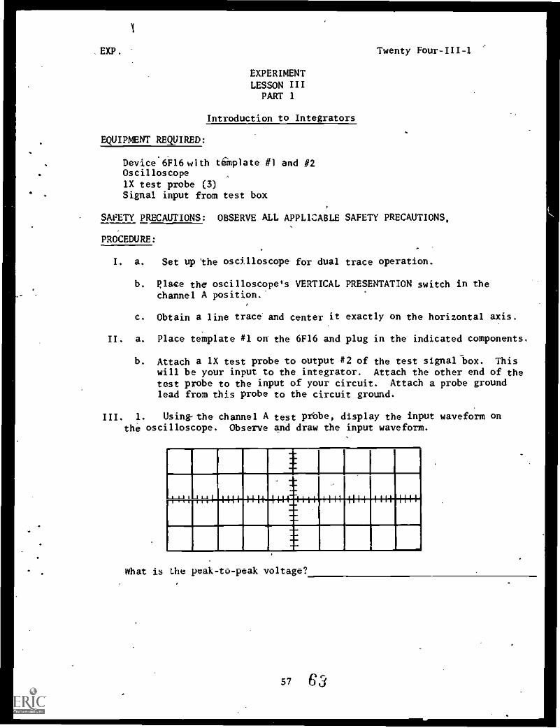
Introduction to Integrators
EQUIPMENT REWIRED:
Device.6F16 with template #1 and #2OscilloscopelX test probe (3)Signal input from test box
SAFETY PRECAUTIONS: OBSERVE ALL APPLICABLE SAFETY PRECAUTIONS,
PROCEDURE:
I. a. Set up 'the oscilloscope for dual trace operation.
b. place the oscilloscope's VERTICAL PRESENTATION switch in thechannel A position.'
c. Obtain a line trace' and center it exactly on the horizontal axis.
II. a. Place template #1 on the 6F16 and plug in the indicated components.
b. Attach a 1X test probe to output #2 of the test signal box. Thiswill be your input to the integrator. Attach the other end of thetest probe to the input of your circuit. Attach a probe groundlead from this probe to the circuit ground.
III. I. Using-the channel A test probe, display the input waveform onthe oscilloscope. Observe and draw the input waveform.
L
1111 1111 1111,1111 411 1111 1411 111
What is Like peak-to-peak voltage?
57 63

EXP. Twenty Four-III-1
2. a. Place the oscilloscope's VERTICAL PRESENTATION switchin the channel B position and obtain a line trace.
b. Center the line trace exactly on the horizontal axis.
c. Using the channel B test probe, observe and draw the output wave-form.
What is the peak-to-peak voltage?
3. Is this an integrator or a differentiator?
4. Place the vertical position switch in the chopped position. Ob-serve and drawthe waveforms.
t el/ I eI I if I Ole 'III
Notice how much the output is attenuated? This is because thecapacitor is not being allowed to charge fully during each halfcycle.
CHECK YOUR RESPONSES WITH THE ANSWERS PROVIDED IN THE BACK OF THISBOOKLET. WHEN YOUR RESPONSES AGREE WITH THE ANSWERS, PROCEED TOPART 2 OF THIS JOB SHEET.
IF YOUR RESPONSES DIFFER FROM THOSE GIVEN, RECHECK YOUR SETTINGS AND ,-PROCEDURES. IF YOU STILL HAVE A PROBLEM, SEE YOUR LEARNING SUPER-VISOR.
6458
EXP. Twenty Four-III-2
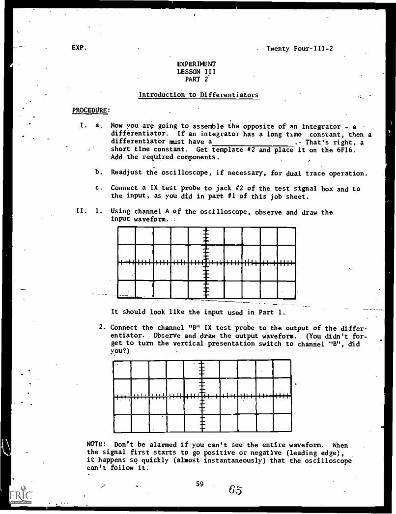
EXPERIMENTLESSON IIIPART 2
Introduction to Differentiators
PROCEDURE:
I. a. Now you are going to assemble the opposite of an integrator - adifferentiator. If an integrator has a long tato constant, then adifferentiator must have a .- That's right, ashort time constant. Get template #2 and place it on the 6F16.Add the required components.
b. Readjust the oscilloscope, if necessary, for dual trace operation.
c. Connect a IX test probe to jack #2 of the test signal box and tothe input, as you did in part #1 of this job sheet.
II. 1. Using channel A of the oscilloscope, observe and draw theinput waveform.
F4111
.11111.
11114111 1111
=NM:Mr
1111
It should look like the input used in Part 1.
2. Connect the channel "B" IX test probe to the output of the differ-entiator. Observe and draw the output waveform. (You didn't for-get to turn the vertical presentation switch to channel "B", didyou?)
_sit ill.1.1 1411 1111 1114 11 1141 1111
NOTE: Don't be alarmed if you can't see the entire waveform. Whenthe signal first starts to go positive or negative (leading edge),it happens so quickly (almost instantaneously) that the oscilloscopecan't follow it.
596:5
EXP. Twenty Four-III-2
3. What is the output peak-to-peak voltage?
4. Now, locate a 33 K ) resistor and put in place of the 4.7 K uresistor. What %.6!1 happen to *_die output? It is now morc/lensdifferentiated? Old the output ampiitud. increase or Zaregiii-sh:aply? Ry how xuch?
5. Now replace the 33 K a resiszot. 0,q. a 10 t n resistor.. Whichresistor (33 K Q 10 K a, or 4.7 K 1.;!oduced the "best" dif-ferention?
6. You have now built RC integratcrs and differentiators and lookedat the inputs and outputs of each. This leaves only the L/R typecircuits (integrators and differentiatcrs.)' You-will not be ableto construct these as the 6F16 doesn't have these capabilities.Remember how they were covered in The written media? L/R circuitsproduce the same outputs as RC circuits. The only difference iswhere you take the outputs.
This concludes the Experiment on Integrators and Differentiators. Se-.cure the test equipment and put all.the components back in their properplaces.
CHECK YOUR RESPONSES WITH THE ANSWERS PROVIDED IN THE BACK OF THISBOOKLET. WHEN YOUR RESPONSES AGREE WITH THE ANSWERS YOU MAY TAKELESSON III PROGRESS CHECK. IF YOU FEEL THAT YOUR PROGRESS CHECK RESULTSINDICATE THAT YOU ARE READY TO TAKE THE END OF MODULE TESTS, SEE YOURLEARNING SUPERVISOR. IF YOU FEEL YOU NEED FURTHER STUDY BEFORE TAKINGTHE END OF MODULE TESTS, YOU MAY REVIEW' ANY PART OF THIS MODULE.IF YOUR RESPONSES DIFFER FROM THOSE GIVEN, RECHECK YOUR SETTINGS ANDPROCEDURES. IF YOU STILL HAVE A PROBLEM, SEE YOUR LEARNING SUPERVISOR.
6660

P.C. Twenty Four-III
PROGRESS CHECKLESSON III
Integrators and Differentiators
1. An RC integrator's output iitaken across th
2. An L/R integrator'S output is taken across the
3. An RC differentiator's output is taken across the
4. An L/R differentiator's output is takg across the
S. An integrator has a long/short time constant with respect to theinput pulse.
6. A differentiator has a long/short time.constant with respect tothe input pulse.
7. Which of the illustrated output waveforms-indicates The shortesttime constant?
a.
b.
c.
d.
8. Which of the illustrated output waveformi.indicates the.longesttime constant? )
a.
b .
. C.
d.
67'61
1

feM
P.C. Twenty Four-III.
9. Match the illustrated circuits withtheir most correct names.
M.. mos Am
0 NA.At
#1.1, SEC
5004
'a. Tcm500 u sec
alb mg .a. Mb. .,=P
100/1 SEC
b. TC=5 usec
50A.1, SEC
c. TORS m sec
w
.1100
)U SEC
d. TC=10'usec
0
o-
1. - L/R differentiator2. RC differentiator3. L/R integrator4. RC integrator
CHECK YOUR RESPONSES WITH THE ANSWERS PROVIDED IN THE BACK OF THIS
BOOKLET. WHEN YOUR'RESPONSES AGREE WITH THE ANSWERS, PROCEED TOEND OF MODULE TEST.
6&62
.1
. .
r.

MODULE
TWENTY FIVE
SPECIAL DEVICES
63 69.

EXP. Twenty Five-I-1
EXPERIMENTLESSON IPART 1
Silicon Controlled Rectifier DC Control
This Experiment will demonstrate the operation of an SCR when for-ward bias is applied from a DC source.
EQUIPMENT REQUIRED:
Device 6F16 with template "J" - introduction to SCR's.
PROCEDURE:
1. Set up Device 6F16 using template #J and the pirts called for bythe template. Observe all applicable safety precautions.
NOTE: Do not install jumper "F". Do not energize the device.
2. When this circuit is energized, will DS1 light?
3. Now energize the 6F16 using the line cord.
4. Why is the light out at this time?
a. The SCR is forward biased.b. The SCR is reverse biased.c. There is no gate voltage applied.d. There is a positive gate voltage applied.
S. What will happen if jumper "F" is installed?
a. The SCR will cut off.b. The SCR will conduct.c. The light will remain off.
6. Install Jumper "F".
7. What did jumper "F" do to the circuit?
a.
b.
c.
d.
Forward biased the SCR.Reverse biased the SCR.Applied a negative voltageApplied a positive voltage
to the gate lead.to the gate lead.
8. If jumper "F" is removed, will the light go out?
9. Remove jumper "F".
70 64

EXP. Twenty Five-I-1
10. Now that the SCR is conducting, how can the circuit be restoredto it's "off" condition?
a. Apply a positive voltage to the gate.b. Remove the gate voltage:c. Remove jumper "C".d. Apply a ground to the gate lead.
11. Test 'your answer to #10 by momentarily performing the action youchose.
NOTE: If you chose answer "A" obtain the voltage from the bottomof resistor R2. DO NOT apply full positive voltage to the gatelead. The SCR may biaamaged if a high voltage is applied to thegate.
12. If the light goes off and remains off when the circuit is restored,your answer to #10 is correct. If the light is still lit, go backto #10 and try again.
CHECK YOUR RESPONSES WITH THE ANSWERS PROVIDED IN THE BACK OF THISBOOKLET. WHEN YOUR RESPONSES AGREE WITH THE ANSWERS, PROCEED TO PART2 OF THIS JOB SHEET.IF YOUR RESPONSES DIFFER FROM THOSE GIVEN, RECHECK YOUR SETTINGS ANDPROCEDURES. IF YOU STILL HAVE A PROBLEM, SEE YOUR LEARNING SUPERVISOR.
65 71
EXP. Twenty Five-I-2
EXPERIMENTLESSON IPART 2
Silicon Controlled Rectifier AC Control
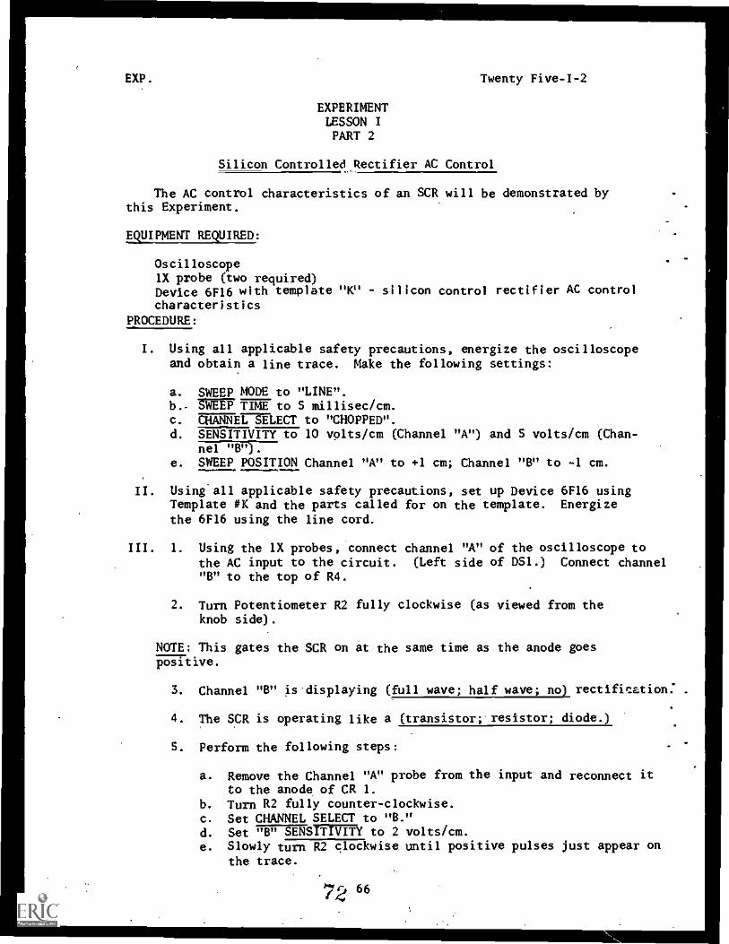
The AC control characteristics of an SCR will be demonstrated bythis Experiment.
EQUIPMENT REQUIRED:
Oscilloscope1X probe (two required)Device 6F16 with template "K" - silicon control rectifier AC controlcharacteristics
PROCEDURE:
I. Using all applicable safety precautions, energize the oscilloscopeand obtain a line trace. Make the following settings:
a. SWEEP MODE to "LINE".b.- SIEUTIME to S millisec/cm.c. WARRENtEcT to "CHOPPED".d. SENSITIVITY to 10 volts/cm (Channel "A") and S volts/cm (Chan-
10"EW57e. SWEEP POSITION Channel "A" to +1 cm; Channel "Et" to -1 cm.
II. Using all applicable safety precautions, set up Device 6F16 usingTemplate #K and the parts called for on the template. Energizethe 6F16 using the line cord.
III. 1. Using the 1X probes, connect channel "A" of the oscilloscope tothe AC input to the circuit. (Left side of 051.) Connect channel"Et" to the top of R4.
2. Turnknob
NOTE: Thispositive.
Potentiometer R2 fully clockwise (as viewed from theside).
gates the SCR on at the same time as the anode goes
3. Channel "Et" is displaying (full wave; half wave; no) rectificEtion:
4. The SCR is operating like a (transistor; resistor; diode.)
S. Perform the following steps:
a. Remove the Channel "A" probe from the input and reconnect itto the anode of CR 1.
b. Turn R2 fully counter-clockwise.c. Set CHANNEL SELECT to "B."d. Set "Et" SENSTTTVITY to 2 volts/cm.e. Slowly turn R2 clockwise until positive pulses just appear on
the trace.
2 66

EXP. Twenty Five -I -2
f. Set HORIZONTAL POSITION until the leading edge of the middlepulse coincidesMaFite vertical center line of the graticule.The leading edge of the pulse is the "turn on" time of the SCR.
g. Set CHANNEL SELECT to "A".
h. Set "A" SENSITIVITY to 2 volts/cm.
i. Using Channel "A" POSITION set the positive peaks of the sinewave at the horizontal center line of the graticule. The hori-zontal center line of the graticle now represents the "turnon" voltage for the SCR. 'This is a representation of thevoltage applied to the gate lead of the SCR.
Set the CHANNEL SELECT SWITCH to "CHOPPED." The sweeps willbe superimposed, so remember which waveform is the input andwhich is the output.
6. What happens to the SCR when the voltage to the gate reaches thehorizontal centerline of the graticule? The SCR (cuts off; con-ducts).
7. Turn R2 clockwise until the peak voltage displayed on Channel "A"reaches +.2 cm. (One small division above horizontal centerline.)
8. The gate voltage now reaches "turn on" voltage (earlier; later;at the same time)in the applied sinewave.
9. The SCR is now conducting (more; less; the same).
10. Turn R2 clockwise until the peak voltage to the gate is at +.6 cm(three small divisions above the centerline.) What happened to
. the conduction time of the SCR? The conduction time (increased;decreased; remained the same).
11. Which of the statements below best describes the action of the SCRtn this circuit?
a. SCR conduction begins at the time the gate signal reaches the"Turn on" voltage level.
b. SCR conduction increases when the gate voltage increases.
CHECK YOUR RESPONSES WITH THE ANSWERS PROVIDED IN THE BACK OF THISBOOKLET. WHEN YOUR RESPONSES AGREE WITH THE ANSWERS, PROCEED TOLESSON I PROGRESS CHECK.
IF YOUR RESPONSES DIFFER FROM THOSE GIVEN, RECHECK YOUR SETTINGS ANDPROCEDURES. IF YOU STILL HAVE A PROBLEM, SEE YOUR LEARNING SUPERVISOR.
67 73
P.C. Twenty Five-I
PROGRESS CHECKLESSON I
Introduction to Silicon Controlled Rectifiers
1. SCR's are not affected by
a. heat.
b. vibration.c. cold.
d. current.
2. The SCR is similar to a
3. The three leads of an SCR are theand the
, the
4. The bias conditions necessary to start an SCR into
a. positive on the anode, negative on the cathodeb. negative on the anode, positive on the cathodec. positive on the anode, negative on the cathode
the gate.d. negative on the anode, positive on the cathode
the gate.
conduction are
, and positive on
, and negative on
S. The bias conditions necessary to maintain an SCR in conductionarea. positive on the anode, negative on the cathode.b. negative on the anode, positive on the cathode.c. negative on the anode, positive on the cathode, and positive on
the gate.d. positive on the anode, positive on the cathode, and positive on
the gate.
6. The direction of current flow through a conducting SCR is
a. cathode to anode.b. anode to cathode.c. gate to anode.d. cathode to gate.
7. One way to stop conduction of an SCR is to
a. remove the gate signal.
b. reverse bias the SCR.c. increase forward bias.d. grourid the cathode.
7 68
P.C. Twenty Five-I
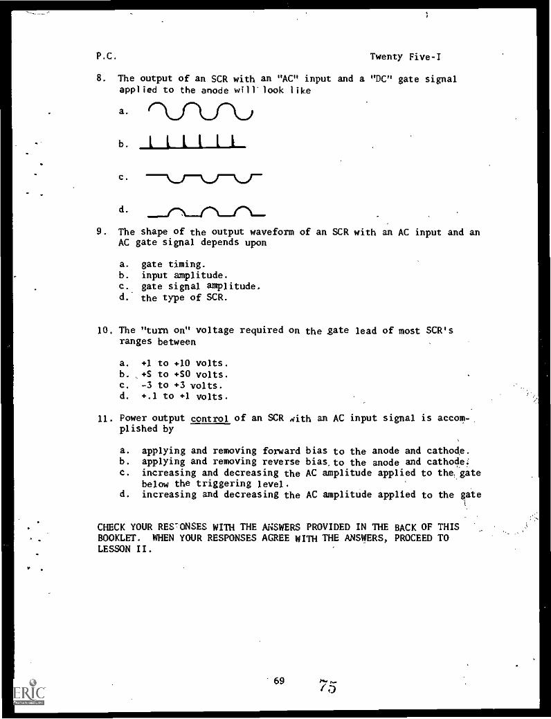
8. The output of an SCR with an "AC" input and a "DC" gate signalapplied to the anode will'look like
a.
b. LIL111
d.
9. The shape of the output waveformAC gate signal depends upon
a. gate timing.b. input amplitude.c. gate signal amplitude.d.* the type of SCR.
of an SCR with an AC input and an
10. The "turn on" voltage required on the gate lead of most SCR'sranges between
a. +1 to +10 volts.b. +5 to +SO volts.c. -3 to +3 volts.d. +.1 to +1 volts.
11. Power output control of an SCR iiith an AC input signal is accom-plished by
a. applying and removing forwardb. applying and removing reverseC. increasing and decreasing the
below the triggering level.d. increasing and decreasing the
bias to the anode and cathode.bias, to the anode and cathode:AC amplitude applied to thegate
AC amplitude applied to the gate
CHECK YOUR RES-ONSES WITH THE ANSWERS PROVIDED IN THE BACK OF THISBOOKLET. WHEN YOUR RESPONSES AGREE WITH THE ANSWERS, PROCEED TOLESSON II.
69 75
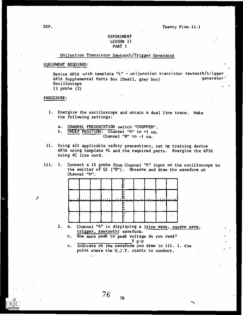
EXP. Twenty Five-II-1
EXPERIMENTLESSON IIPART 1
Unijuction Transistor Sawtooth/Trigger Generator
EQUIPMENT REQUIRED:
Device 6F16 with template "L" -.unijunction transistor sawtooth / trigger
6F16 Supplemental Parts Box (Small, grey box) generator'
Oscilloscope1X probe (2)
PROCEDURE:
I. Energize the oscilloscope and obtain a dual line trace. Makethe following settings:
a. CHANNEL PRESENTATION switch "CHOPPED".b. SWEEP POSITION: Channel AS to +1 cm.
Channel "B" to -1 cm.
II. Using all applicable safety precautions, set up training device6F16 using template #L and the required parts. Energize the 6F16using AC Iine cord.
III. 1. Connect a 1X probe from Channel "A" input on the oscilloscope tothe emitter of QI ("D"). Observe and draw the waveform onChannel "A".
2. a. Channel "A" is displaying a (sine wave, square wave,trigger, sawtooth) waveform.
b. How much peak to peak voltage do you read?V p-p
c. Indicate on the waveform you drew in III. 1. thepoint where the U.J.T. starts to conduct.
:670

EXP. Twenty Five-II-1
3. Connect a 1X probe from channel "B" input on the oscilloscopeto base 1 of Q1 ("C"). Observe and draw the waveforms.
1111 1111
4. a. Channel "8" is displaying a (sine wave, square wave,trigger, sawtooth) waveform.
b. How much peak to peak voltalge do you ,read? vp-pc. The U.J.T. is at its highest conduction when the waveform at
81 is (not present, most positive, least positive).
5. a. From this job sheet you can see that you get two verydifferent types of waveforms at different points on theU.J.T. By connecting the oscilloscope input to the emitter,you see a (sine wave, square wave, trigger, sawtooth)output.
b. By connecting the scope to based a (sine wave, squarewave, trigger, sawtooth) is viewed.
CHECK YOUR RESPONSES WITH THE ANSWERS PROVIDED IN THE BACK OF THISBOOKLET. WHEN YOUR RESPONSES AGREE.WITH THE'ANSWERS, PROCEED TO PART2 OF THIS JOB SHEET.IF YOUR RESPONSES DIFFER FROM THOSE GIVEN, RECHECK YOUR SETTINGS ANDPROCEDURES. IF YOU STILL HAVE A PROBLEM, SEE YOUR LEARNING SUPERVISOR.
71

EXP. Twenty Five-II-2
EXPERIMENTLESSON IIPART 2
Unijunction Transistor Multivibrator
EQUIPMENT REQUIRED:
Device 6F16 with template "M" unijunction transistor multivibrator6F16 Supplemental Parts Box (small, grey box)OscilloscopelX Probe (2)
PROCEDURE:
I. Energize the oscilloscope and obtain a dual line trace. Make the
following' settings.
a. CHANNEL PRESENTATION switch to "CHOPPED"b. SWEEP POSITION: Channel "A" to + 1 cm.
Channel "B" to -1 cm.
II. (4ing all applicable safety precautions, set up training device6116 using template #M and the required parts. Energize the 6F16
using the AC line cord.
III. Connect a 1X probe from the oscilloscope Channel "A" input to base
2 ("F") of Ql.
1. a. Observe and draw the waveform appearing on channel "A".
_t
b. Channel "A" is displaying a (sine wave, square wavetrigger, sawtooth) waveform.
c. How much peak to peak voltage do you read? Vp-p
72

(/ EXP: Twenty Five-TI-2
2. Connect a lx probe from Channel "B" input on the oscilloscope to thecathode of CR1.
3. a. Observe and draw the waveform shown on channel "8".
11.
1'1 ±H14
'NB
.11m
1111 1111- 1111k
b. The waveform on channel "B" is displaying a (sine wave,square wave, trigger, sawtooth).c. How much peak to peak voltage do you read? Vp-pd. Q1 begins to conduct at volts.
4. Place the 1X probe from channel "B" input to the anode of CR 1.
S. a. Observe and draw the waveform on channel "B".
,1 '1 1 111 IIH 1111 11-11 1
A
If If illi 1111 11!
b. Is the waveform different than the waveform on the cathode?c. Why?
6. What is the relationship of the conduction and cutoff times of Qland CR 1?a. Ql not conducting, CR1 not conducting.b. Ql conducting, CR1 not conducting.c. Ql conducting, CR1 conducting.
7. Notice that once again the U.J.T. provides two very different typesof outputs.
7379

b
EXP. Twenty FiveII-2
8. In the circuit on template #M, Base 2 provides a
a. square wave.b. sine wave.c. trigger.d. sawtooth.
9. In the circuit on template #M, the emitter provides a
a. square wave.b. sine wave.c. trigger.d. sawtooth.
CHECK YOUR RESPONSES WITH THE ANSWERS PROVIDED IN THE BACK OF THISBOOKLET. WHEN YOUR RESPONSES AGREE WITH THE ANSWERS YOU HAVE COMPLETEDTHIS MODULE. IF YOU FEEL THAT YOUR PROGRESS CHECK RESULTS INDICATETHAT YOU ARE READY TO TAKE THE END OF MODULE TEST, SEE YOUR LEARNINGSUPERVISOR. IF.YOU FEEL YOU NEED FURTHER STUDY BEFORE TAKING THE ENDOF MODULE TESTS, YOU MAY REVIEW ANY PART OF THIS MODULE.IF YOUR RESPONSES DIFFER FROM THOSE GIVEN, RECHECK YOUR SETTINGS ANDPROCEDURES. IF YOU STILL HAVE A PROBLEM, SEE YOUR LEARNING SUPERVISOR.IT IS SUGGESTED YOU TAKE THE PROGRESS CHECK FOR LESSON II PRIOR TOTAKING THE END OF MODULE TEST.
ti
74

..0.00
Exp. Twenty Five-II-3
EXPERIMENTLESSDN 11
PART 3
UJT Ramp Generator and SCR Control Circuit
The experiment will demonstrate the operation ,of the NIDA 204 FunctionGenerator's UJT Oscillator PC board*and the SCR Control PC board. Youwill also be shown how these two circuits operate together in a system.
EQUIPMENT REQUIRED:
NIDA 204 Function Generator
Oscilloscope
Signal Generator
BNC-BNC Cables f2)
IX Probe (2)
Jumper Cable with alligator clips (1)
REFERENCE MATERIAL:
PC 204 and 1 thru 8 Printed Circuit Cards
Function Generator, NIDA Trainer, Model 204, Instruction Manual.
PROCEDURE:
I. Energize the oscilloscope and set it up for CHANNEL A and INTERNAL MOOEoperation. Using a BNC-BNC cable connect the NIDA Function GeneratorOUTPUT jack to CHANNEL "A" of.the oscilloscope. Energize the signalgenerator to warm up for later use.
2. Set up-the NIDA 204 Function Generator front panel controls as follows:
a. TRIGGER to "Internal."b. FREQUENCY switch to "1000 Hz."c. FREQUENCY dial to "3."d. OUTPUT LEVEL fully clockwise.e.' SYMMETRY full clockwise.f. FUNCTION switch to (Ramp)
3. Remove the top cover of the NIOA 204 and ensure all eight PC cards arein place.
4. Plug in and energize the Function Generator.)
.0
75

as,
Exp. Twenty Five-II-3
Observe the output waveform from the Function Generator. The outputshould be a ramp (sawtooth) voltage with a smooth (straight line) rise.The basic UJT oscillator in your study booklet had an "integrated"(curved line) output. The UJT oscillator in the NIDA 204 has someadditional circuits that make the output linear.
Refer to Figure 1 in this experiment and locate PC 204-6. This is aschematic of the UJT Oscillator - Ramp Generator.
NOTE: Transistor Q1-6 and its associated circuitry (R2-6, CR1-6, CR2-6,CR3-6;and R1-6) comprise a "Current Regulator." This current regulatorwill maintain current through the UJT Emitter Capacitor's at a con-stant value resulting 4n a linear "Ramp" output.
. Transistor Q3-6 is another device you are probably not familiar with..0 It is called a "Field Effect Transistor," or, to shorten the name a bit,
FET. This FET and its associated components (R6-6 and R7-6) make up anamplifier circuit. An FET is used as an amplifier because it has ahigh input impedance and will not loadthe UJT_ circuit. If a regulartransistor were used in place of the FET, the output would be dis-torted. ,..
Refer to Figure 1 and answer the following questions:
(I) The FREQUENCY SWITCH (S2) will change the (capacitance/resistance) -of the UJT oscillator.
..--s (2) With the FREQUENCY SWITCH (S2) in the 1000 Hz position, capacitor(C9/C10/C11/C12) is in (series/parallel) with Cl -6.
8. Tha FREQUENCY dial (1121A) sets the conduction level of the currentregulator. If the regulated current increases, the capacitors in theemitter circuit of the UJT will chave more quickly and increase the.output frequency.
(1) The FREQUENCY potentiometer (R21A) is in (series/parallel) with R2-6.
Now that we have checked the operation of the UJT circuit,. let's take a lookat the SCR control circuit operation. (Reit.- to Figure 1 and locate PC 204-5SCR control Circuit).
9. Deenergize and unplug the NIDA 204 Functic.a Generator. .
10. Remove the Unijunction Oscillator printed circuit card PC204-6..
11. Connect a IX probe to the oscilloscope's CHANNEL B. input and set upthe oscilloscope for CHANNEL "B", INTERNAL TRIGGER mode.
12. Plug in and energize the NIDA 204 Function Generator.

114
O
Twenty Five-II-1
13. Using the oscilloscope, measure and record the DC voltages at theanode and cathode of SCR2-5.
(1) Anode: VOC
(2) Cathode: VOC(3) Is SCR 2-5 conducting? (YES/NO)
Alw
HINT: Whenever the difference in potential between the anode and cathodeof an SCR exceeds 0.6 volts, the SCR is not conducting.
(4) Is SCR 2-5 forward biased?
(5) What else is required to turn 3n SCR 2-5?
a. Reverse bias SCR 2-5.b. Forward bias SCR 2-5.c. Apply a positive signal to SCR.2-5's gate lead.d. Apply a negative signal v3 SCR 2-5's gate lead.
14. Now we are going to turn SCR 2-5 on by aN.Iying a positive signal to thegate lead: De-energize NIDA 204 and connect one lead of a jumper to PC204-7, pin 3, and leave the other end free. Energize and momentarilytouch the free end to PC 204-5, pin 10.(1) Is SCR 2-5 conducting? (YES/NO)
15. Place ...the 1X probe at the SCR 1-5 gate lead. Carefully observe theoscilloscope trace for a "pulse" while rapidly pressing and releasingthe TRIGGER SWITCH (S5).
NOTE: The TRIGGER SWITCH will be in the "MAN" (manual) positionwhen depressed and is spring, loaded to return to the "EXT"(external) position wh4n released. Use the .5v/cm. positionon the Oscilloscope Channel B.
(1) The signal applied to the gate lead of SERI -5 when the TRIGGERSWITCH is depressed is a
a. positive going trigger.b. negative-going trigger.
NOTE: The trigger switch'applies a negative signal to the base oftransistor Ql. The signal is differentiated, inverted and
, applied to the gate lead of SCR 1-5. (Refer to Figure 1.)
16. Move the 1X probe to the anode of SCZ 1-5. Carefully observe theoscilloscope trace while depressing and releasing the TRIGGER S4&TCH(S5) .
77 83

Exp. Twenty Five-II-3
(1) When the TRIGGER SWITCH (S5) is placed in the "MAN" (manual)position SCR 1-5
a. "turns off" momentarily then "turns on" again.b. "turns on" momentarily then "turns off" again.
NOTE: When SCR 1-5 conducts, capacitor C2 -5 will discharge throughCR1-5 and SCR1-5. Resistor R6 -5 in the anode circuit ofSCR1-5 is a high value resistor. There is insufficient cur-rent through R6-5 (holding current) to maintain SCR1-5 inconduction. SCR1-5 will "shut off" when capacitor C2-5 isdischarged. The discharge path for C2-5 is through theforward biased CR1 -S and SCR1-5.
17. Move the )X probe to the anode of SCR 2-5.
(1) Is SCR 2-5 conducting? (TES/NO)
18. Turn on SCR 2-5. (Momentarily connect a jumper between PC204-7, On 3,and PC204-5, pin 10.)
19. While observing the oscilloscope trace, place the TRIGGER SWITCH (S9)to "MAN". This action causes SCR1-5 to conduct, discharges C2-5and drives the anode of SCR2-5 negative; thereby shutting SCR2-5"off."
We will now see how the SCR Control Circuit and the UJT Oscillator-RampGenerator work together.
20. Deenergize the NIDA 204 Function Generator and insert the UJTOscillator-Ramp Generator printed circuit card, PC204-6.
21. Ensure the NIDA 204 Function Generator is set up'as follows:
a. FREQUENCY SWITCH (S2) to "1000 Hz."b. FREQUENCY DIAL (R21A) to ,,3.0c. TRIGGER SWITCH (S5) to "INT."d. INPUT SENSITIVE CONTROL fully clockwise.e. TRIGGER LEVEL fully counter clockwise.f. OUTPUT LEVEL fully clockwise.g. FUNCTION SWITCH to
22. Using a BNC-BNC cable, connect the Audio Output from the Signal Genera-tor to the input of the NIDA 204. Set up the Signal Generator as
follows:
a. METER READS switch to "Z.00 Hz."b. AUDIO OUTPUT to read 5 on the microvolt scale.
78
84

Exp. Twenty Five-II-3
23. Energize the NIDA 204. Set up the oscilloscope for CHANNEL A - Observethe waveform on the oscilloscope, then replace the TRIGGER switch (S5)on the NIDA 204 to "EXT."
(1) The number of ramps displayed on the oscilloscope (increased/decreased/remained the same).
NOTE: The number of ramps displayed decreased because placingthe TRIGGER SWITCH (S5) to "EXT." allowed the SCR controlcircuit to control the 11.1T Oscillator - Ramp Generator. (Figure1 shows the interconnection between the 11.1T and SCR circuitsyou have just studied.)
24. Place the oscilloscope's CHANNEL "B" probe on Base 1 of the 11.1T (Q2-6).Look closely for a positive trigger.
NOTE: Set up the osc..loscope as follows to better observe thetrigger:
a. CHANNEL MODE SWITCH to "chopped."b. SWEEP MODE to "Internal."c. SWEEP TIME to ".5 millisecond/CM."d. CHANNEL "A" SENSITIVITY to "5 volts/CM."e. CHANNEL "B" SENSITIVITY to "1 volt/CM."
(l) The positive trigger from Q2-6 base I will cause SCR 2-5 to(conduct/turn off).
NOTE: When the TRIGGER SWITCH (S5) is in the "External" positionand SCR2-5 conducts, the 11.1T circuit cannot generate anotherramp.
25. Place the CHANNEL "B" IX probe on the gate lead of SCR 1-5.
This signal originating from the signal generator (external input) willturn SCR1-5 (on/off).
NOTE: When SCR1-5 turns "on," SCR2-5 turns "off" and another rampwill be generated by the 11.1T circuit. Therefore, using anSCR control circuit allows us to determine when a ramp willbe generated.
CHECK YOUR RESPONSES WITH THE ANSWERS PROVIDED IN THE BACK OF THIS BOOKLET.IF YOUR RESPONSES DIFFER FROM THOSE GIVEK, RECHECK YOUR SETTINGS AND PRO-CEDURES. IF YOU STILL HAVE A PROBLEM, SEE YOUR LEARNING SUPERVISOR.
WHEN YOUR RESPONSES AGREE WITH THE ANSWERS GIVEN ;ND YOU FEEL THATYOU HAVE MASTERED THE MATERIAL IN THIS EXPERIMENT, REPLACE ALL THE COVERSAND RETURN YOUR EQUIPMENT TD ITS STOWAGE, TI.IEN PROCEED TO THE PROGRESSCHECK.
79 65

I n1E11.1!ITI.I!P.I.;
MONAS, Norfolk, Virginia 23511
U.S. Naval Safety Contor,
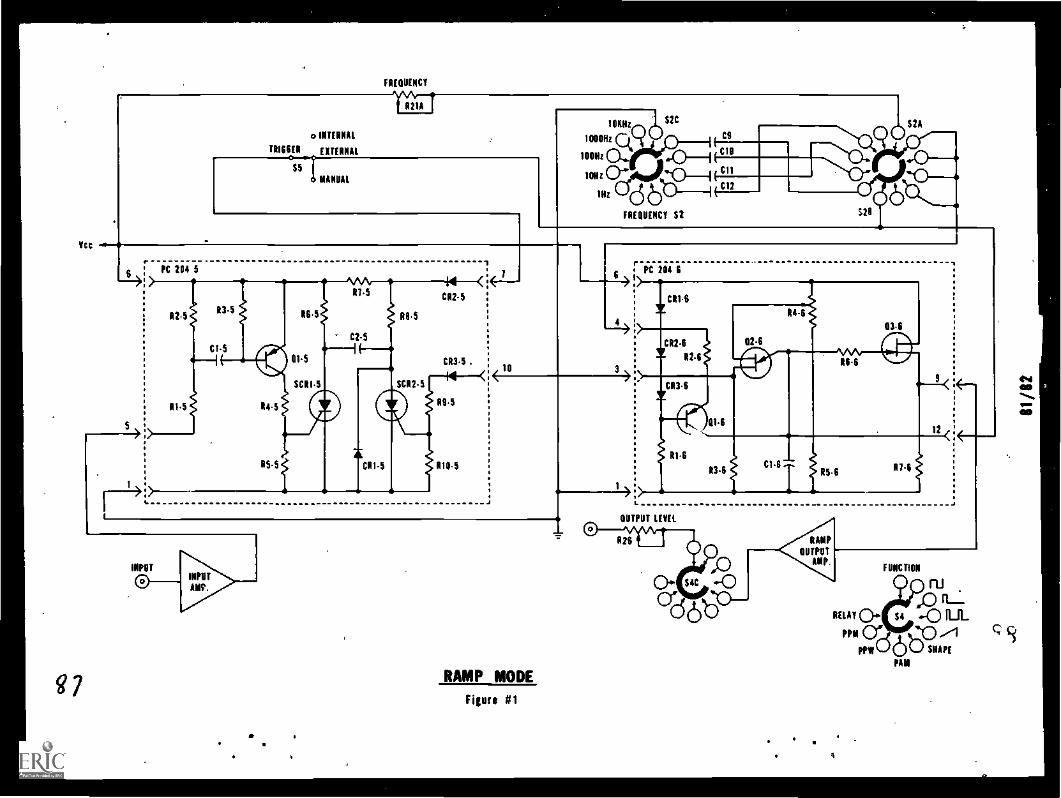
ICC
S7
FIEOUENCY
rPC 204 5
*INTERNAL
TRIMI EXTERNAL
71 MANUAL
lt21A
10KNz (...12152C
100Nz
1000Hz C61 Cg
0, .0_1 C111
1°111 $1,111-1 "IN (-Cj
FIEOUENCY 52
0,ci',4 1:0/--.0... ...o--'0- -0--UR
I.
OUTPUT LEVEL
. .
RAMP MODE
Figure #1
RAMP
OUTPUTAMP.
FUNCTION
rugrp rt_
RELAY 00 54 4.8.....111-11..
"10C:dab SHAPE
4
PAM

t
P.C. Twenty Five-II
PROGRESS CHECKLESSON II
Introduction to U.J.T.
1. Label the leads on the schematic symbol of the'U.J.T.
0 00
2. The material between the bases of the U.J.T. acts as a
3. The emitter of the U.J.T. must be in respect tothe in order for the U.J.T. to conduct.
4. The sequential rise in potential between Base 1 and Base 2 iscalled a/an
5. The small amount of current flow in a reverse biased U.J.T. iscalled
6. What is the conduction point of the U.J.T. shown below?
$389

et
P.C. Twenty Five-II
7. What does the waveform at TP "B" look like in the circuit shownbelow? Vcc
a.
b.
c.
d
111111._
8. The shape of the waveform at TP "C" in figure 1 is-determined bythe
a. on/off state oi Ql.b. on/off state of CR1.c. time constant of Cl, R2.d. time constant of CR1, Rl.
ail
84

P.C. Twenty Five-II
9. The waveform at TP "A" in the circuit shown in figure 2 looks like:
+VCC
RI R2
a.
b.
C.
d.
C1
43'
Figure .2
7\7\7LLLLL
A
10. The frequency of the waveform at TP "A" in figure s determinedby
a. Ql.
b. Rl.
c. R2.
d. R3.
85

P.C. Twenty Five-II
In the circuit shoe! in figure 3 CI charges through
a. Q1's BI - B2 junction.b. Q1's E - B2 junction.c. QI's E BI junction.d. ground.
12. The current that charges CI is called
CHECK YOUR RESPONSES WITH THE ANSWERS PROVIDED IN TUE BACK OF THISBOOKLET. WHEN YOUR RESPONSES AGREE WITH THE ANSWERS, PROCEEDTO END OF MODULE TEST.
CO
6

0
/ANSWER SHEETS
FOR
MODULES
TWENTY THREE
TWENTY FOUR
TWENTY FIVE
87
93
.1

c.
EXP. TwentyThree-I
ANSWER SHEETFOR
EXPERIMENTLESSON I
Bistable Multivibrator
NOTE: There are two possible answers to questions 1, 2, 3 and S. Ifyour answer to.#1 is - 4 volts, use the first answer for 2, 3, and S.If yOur.inswer is 0 volts, use the second answer for 2, 3 40 S.
1. -4 volts 0 volts2. 0 volts -4 volts.3. Q2, QI4. slight variations in component values. (or words to that effect)S. NO YES6. yes7. Ql conducting, Q2 cut off8. NO9. YES10. Ql cut off, Q2 conducting
IV.
3.
S.
1111 NI IN
6. The input frequency is twice the output frequency. or words tothat effe.*:t.) 4
88
s
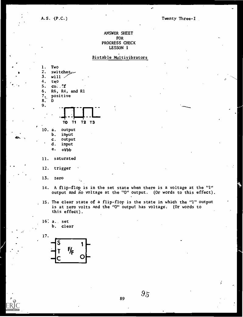
S
,
A.S. F.C.) Twenty Three-1
1. Two2. switches7:3. will4. twoS. cu_.!f6. R6, R4, and R17 positive8.:
9.
ANSWER SHEETFOR
PROGRESS CHECKLESSON
Bistable Multivibrators
TO Tl
10. a. outputb. inputc. outputd. inpute. +Vbb
11. saturated
12. trigger
13. zero
T2 T3
14. A flip-flop is in the set state when there is a voltage at the "1"output and iio voltage at the "0" output. Or words to this effect),
1S. The clear state of a flip-flop is the state in which the "1" outputis at zero volts and the "0" output has voltage. (Or words tothis effect).
16: a.. setb. clear
17.
CT
FF
89
.


A.S. (EXP)
4
Twenty Three-II
ANSWER SHEETFOR
EXPERIMENTLESSON II
Astable Multivibrator (Free Running)
11 iUl 111 1
111111111111111111111111Ii
M2. .64 millisec.
3. .6 millisec.
4.
3111 ,1111 1111 1111 III! 111t
S. .2 millisec
6. .6 millisec
919797

A.S. (P.C.) Twenty Three-II
ANSWER SHEETFOR
PROGRESS CHECKLESSON II
Astable Multivibrators (Free Running)
1. free running
2. oscillator or generator
3. zero (No), two (in that order.)
4. R2 and Cl
S. saturated
6. CI and R2
7. C2
8. b
c
10. b
98.92
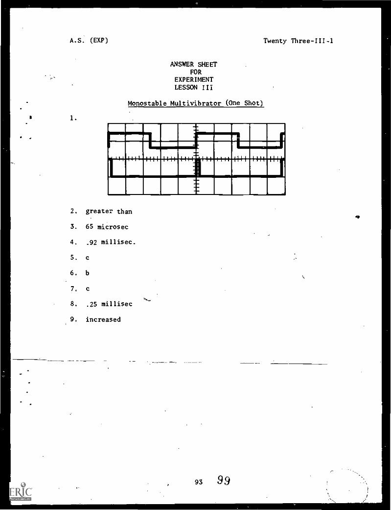
a
.
A.S. (EXP)
I.
Twenty Three -III -1
ANSWER SHEETFOR
EXPERIMENTLESSON III
Monostable Multivibrator (One Shot)
I 'MI LIII III
2. greater than
3. 65 microsec
4. .92 millisec.
5- c
6. b
7. c
8. .25 millisec
9. increased
93 99
4
a

1
Exp. (A.S.)
EXPERIMENTANSWER SHEETLESSON III
PART 2
5.(1) d.
(2) YES
(3) c.
8. Period 37 usec, Frequency 27 KHz (± 10%).
9.
10.
(1) c.
12.
(2) one-half.
(3) c.
(i) b.
(2) a.
(3) b.
(4) d. parallel
(5) c.
(6) Resistance.
.1 Twenty Three-III-2
e.)
. .f
)

0
p
A.g: (P.C.) Twenty Three-III
ANSWER SHEETFOR
PROGRESS CHECKLESSON III
Monostable Multivibrators (One Shot)
1. one2. cut off, saturated (in that order)3. negative4. definite5. input, output (in that order)6. -Vcc7. b
8. f9. c
10. c11. a.12. b13. c14. a15. b16. c17. c18. b
95 101
S

r I Vh 4' A
1 ,1 IA 14,
1 ! OF
PIM rrki 1 1 I

A.S. (EXP). Twenty Four-I-1
4.
S.
6.
7.
vragairiamNEGATIVE CLIPPERCLIPPER with DC aiding forward bias
F
I ,
41.1 t.1441 1111 114f,
4r44
NEGATIVE CLIPPER with DC aiding reverse bias
POSITIVE CLIPPER with DC aiding forward bias
1 111111111/111111111
POSITIVE CLIPPER with DC aiding reverse bias
97 11)3
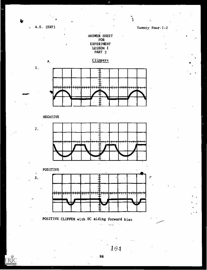
'S
I& Ab 411
I AIL AIL. Noir
IMMII MI . 0 111M MIl or NW .0

I
1
,
k A 0 1. 'LII ! 1 =

A.S. (P.C.)
1. Positive
2. NegatiVe
3. Input
4. Series positive
S. DC
6. C
7. Load or output
ANSWER SHEETFOR
PROGRESS CHECKLESSON
Clippers
.Twenty'Four-I
8. a-4 series positive clipper with positive biasb-1 series negative clipper with positive biasc-8 series positive clipper with negative bias.d-6,series negative clipper with negative biase-7 parallel positive. clipper with positiVe biasf-S parallel negative clipper with,positive biasg-2 parallel positive clipper with negative biash-9 parallel negative clipper with negative biasi-3 parallel positive and negative clipper with positive
and negative bias9. I-a, 2-a, 3-b, 4-a
10. a
+10
011
25b. +25
7
c.
d.
+8OV
e.
f.
10s0 6
011
25
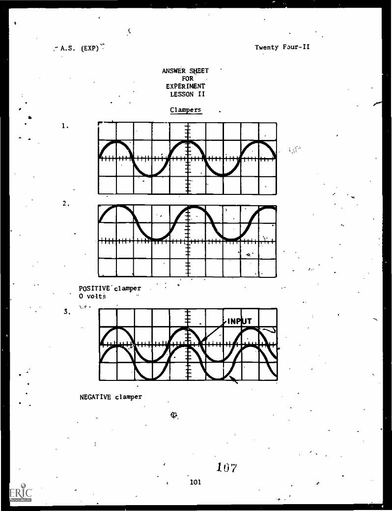
riA lil r 0 rig
I ', A A
- _
1 li
al 1 r kir if -kPAIMPY k. ir i -k 4
ri '. 1

NEI w
..... -diEllea... ...MEM._
r I r I , 1A . A
........-
MEI
4111 , 411k
r 1
MI V 'W' AIM

S.
A.S. (P.C.)
ANSWER SHEETFOR
PROGRESS CHECKLESSON II
Clampers,
I.
2. DC restorer
3. above
4. eS.
S. c
6. time constant
7. a
8. long,
9. b.
Ov10. ,a.
20+50
Ov
+60C. Ov10
+33d. +7
Ov
+13e. Ow37
b.
2gv225
t.
103 ,1094,4 4
Twenty Four-II

A.S. (P.C.) Twenty Four-II
negative clamperpositive clamperpositive clamperpositive clampernegative clampernegative clamper
with negative biaswith positive biaswith positive biaswith negative bias
10411
fj

S
S
-a OP' I
-14.
111."!!'
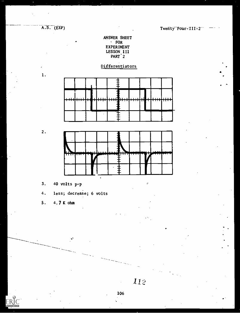
A.S. (tYP)
1.
2.
TwefityFOUr-IIP2--
ANSWER SHEETFOR
EXPERIMENTLESSON III
PART-2
Differentiators
M 111 ME111111111111111111111111.11111111
11111111.11111111111111111
II ME II
MM.
3. 40 volts p-p
4. less; decrease; 6 volts
S. 4.7 K ohm
106
1 1 o-a- 4.
4

A-SCP.C.) Twenty Four-III- _
ANSWER SHEETFOR
PROGRESS CHECKLESSON III
Integrators and Differentiators
1. capacitor
2. resistor
3. resistor
4. coil
S. long
6. short
7. b
8. c
9. a. (4) RC integratorb. (1) L/R differentiatorc. (3) L/R integratord. (2) RC differentiator
1 y3107

8
A.S. (EXP) Twenty Five-I-I
)ANSWER SHEET
FOREXPERIMENTLESSON IPART 1
Silicon Controlled Re .tifier DC Control
2. no ^
4. c. There is no gate voltage applied
S. b. The SCR will conduct.
7. d. Applied 'a positive voltage to the gate lead.
8. no
10. c. Remove jumper "C".
108 114>

A.S. (EXP) Twenty Five-I-2
ANSWER SHEETFOR
EXPERIMENTLESSON IPART 2
Silicon Controlled Rectifier AC Control
3. half wave
4. diode
6. conducts
8. earlier
9. more
10. increased
11. a. SCR conduction begins at the time the gate signal reaches the"Turn on" voltage level.
109

A.S. (P.C.) Twenty Five-I
ANSWER SHEETFOR
PROGRESS CHECK
Silicon Controlled Rectifier Theory
1. b
2. diode
3. gate, anode, cathode (any order)
4. c
S. a
6. a
7. bi
....
8. d
9. a
10. d
11. d
ti.
e,-
4
..

e
a
'
A.S. (EXP) Twenty Five-II-1
'ANSWER SHEETFOR
EXPERIMENTLESSON IIPART 1
U.J.T. Sawtooth Trigger Generator 5
1. waveform taken with oscilloscope: "A" sensitivity .S volts/cmSweep time: 1 milliseconds/ cm
1 1 1 1 I 1 1 11 1111 II alit
2. a. sawtoothb. +.7S volts peak to peakc. (rhe arrows on the above waveform indicate the U.J.T.
conduction points)
3. waveform taken with Oscilloscope: "A" sensitivity: .5'wolts /cm"B" sensitivity: 2 volts/cmSweep Time: 2 milliseconds /cm
4. a. triggerb. +2 volts p-p
c. most positive
S. a. sawtoothb. trigger
111
1 1
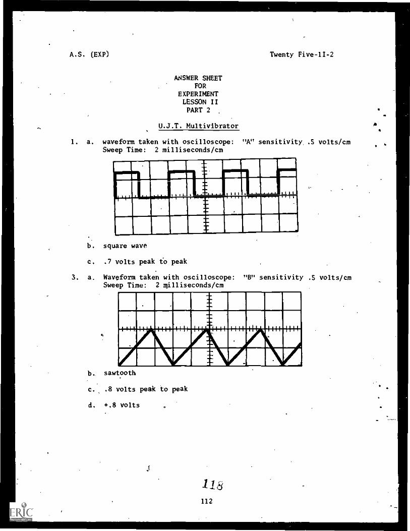
A.S. (EXP)
ANSWER SHEETFOR
EXPERIMENTLESSON IIPART 2
Multivibrator
Twenty Five-1I-2
1. a. waveform taken with oscilloscope: "A" sensitivity, .5 volts/cmSweep Time: 2 milliseconds/cm
. square wave
c. .7 volts peak to peak
3. a. Waveform taken with oscilloscope: "B" sensitivity .5 volts/cmSweep Time: 2 milliseconds/cm
J
11E11111111111111111111111111111111111111111
1112:111111121111PMIPMEWU
b, sawtooth
c., .8 volts peak to peak
d. +.8 volts
118112
A4

4
A.S. (EXP) Twenty Five-II-2
S. a. Waveform taken with oscilloscope: "B" sensitivity .S volts/cmSweep Time: 2 milliseconds /cm.
.d.
NIS
b. yes
c. Because of the halfwave rectification of diode CR1 (or wordsto that effect.)
6. b.
8. a.
d.

,*
.1
Exp.(A.S.) Twenty Five-I1-3
EXPERIMENTANSWER SHEET
LESSON IIPART 3 A
.
4
7. (1) capacitance(2) C12; parallel
A .
8. (1) wies
13. (1)
(2)
(3)
(4)
(5)
22 VDC
0 VDCNoYes
c
(+ 10%)
14. (1) yes
15. (1) a
16. (1) b
17. (1) No
23. (1) decreased
24. (1) conduct
Z5. (1) on
12!)
114
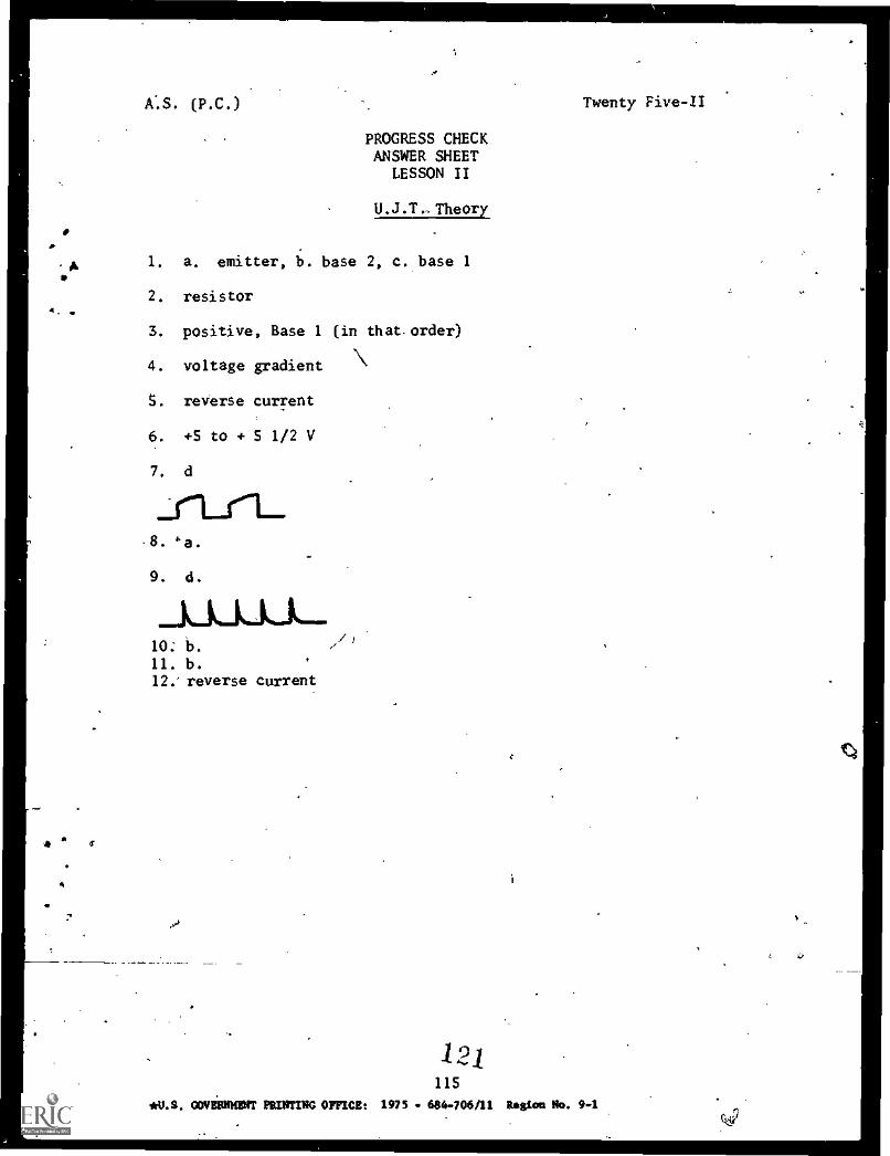
4.
A.V
A.S. (P.C.) Twenty Five-II
PROGRESS CHECKANSWER SHEET
LESSON II
Theory
1. a. emitter, b. base 2, C. base 1
2. resistor
3. positive, Base 1
4. voltage gradient
S. reverse current
6. 4-5 to 4- S 1/2 V
7. d
S
8. 'a.
9. d.
LLLLL10. b.11. b.12.' reverse current
(in that. order)
1 21115
*U. S. 00VNINKINT FRUITING OFFICE: 1975 - 684-706/11 Region No. 9-1