doping optimization for the power factor of bipolar ... · theory and atwo-band model (conduction...
TRANSCRIPT

TOPICAL COLLECTION: INTERNATIONAL CONFERENCE ON THERMOELECTRICS 2018
Doping Optimization for the Power Factor of BipolarThermoelectric Materials
SAMUEL FOSTER 1,2 and NEOPHYTOS NEOPHYTOU1
1.—School of Engineering, University of Warwick, Coventry CV4 7AL, UK. 2.—e-mail:[email protected]
Bipolar carrier transport is often a limiting factor in the thermoelectric effi-ciency of narrow bandgap materials at high temperatures due to the reductionin the Seebeck coefficient and the introduction of an additional term to thethermal conductivity. Using the Boltzmann transport formalism and a two-band model, we simulate transport through bipolar systems and calculatetheir thermoelectric transport properties: the electrical conductivity, theSeebeck coefficient and the thermoelectric power factor. We present aninvestigation into the doping optimisation of such materials, showing thedetrimental impact that rising temperatures have if the doping (and the Fermilevel) is not optimised for each operating temperature. We also show that thedoping levels for optimized power factors at a given operating temperaturediffer in bipolar systems compared to unipolar ones. We show finally that at600 K, in a bipolar material with bandgap approximately that of Bi2Te3, theoptimal doping required can reside between 10% and 30% larger than thatrequired for an optimal unipolar material depending on the electronic scat-tering details of the material.
Key words: Thermoelectrics, thermoelectric power factor, bipolar transporteffects, Seebeck coefficient, optimized doping, Boltzmanntransport theory
INTRODUCTION
The efficiency of thermoelectric (TE) materials(which convert between heat and electricity) isquantified by the figure of merit ZT = rS2T/(jl+ je)where r is the electrical conductivity, S is theSeebeck coefficient, T is temperature, jl is thelattice thermal conductivity and je is the electronicthermal conductivity. The quantity rS2 is termedthe power factor (PF).
Manyof themost importantTE materialsarenarrowbandgap semiconductors.1 These narrow bandgaps(e.g., PbTe � 0.3 eV,2 Bi2Te3 � 0.2 eV,3 SnSe � 0.39eV)4 mean the materials suffer from bipolar effects athigh operating temperatures. The bipolar effect occurswhen both electrons and holes contribute to charge
transport. When this happens: (1) je increases due tocontributions from both electrons and holes, (2) anadditional thermal conductivity term, the bipolar ther-mal conductivity,jbi, is introduced (a result of electron–hole recombination at the contacts),5 which also intro-duces large increases in the Lorenz number,6 (3) theSeebeck coefficient drops as both electrons and holescontribute to it with opposite signs, and (4) the Fermilevel moves towards the midgap in order to conservecarrier concentration, (although it does not fall asquickly as in the unipolar case). The thermal conduc-tivity from (1) and (2) degrades thermoelectric perfor-mance through the denominator of ZT, whereas (3)degrades performance through the numerator.
The optimal thermoelectric performance (for boththe peak PF and peak ZT) depends heavily on thecarrier concentration,7 and this optimal is known tobe temperature dependent, i.e., the performancepeaks at different doping concentrations for differ-ent temperatures.8 However, although it is known(Received August 23, 2018; accepted December 4, 2018;
published online December 18, 2018)
Journal of ELECTRONIC MATERIALS, Vol. 48, No. 4, 2019
https://doi.org/10.1007/s11664-018-06857-1� 2018 The Author(s)
1889

that for unipolar materials the optimized dopingincreases as T3=2,9 the optimization of the carrierconcentration for bipolar systems is not yet clarified.
While various strategies have been suggested toreduce the bipolar effect in order to regain highperformance, such as using heterostructuredesigns,10,11 band engineering to widen the band-gap,12,13 and grain boundaries with barriers forminority carriers,14 in this work we show thatconsidering proper doping optimization by takinginto account the bipolar effects could also allow forperformance improvements.
For this, in this work we use Boltzmann transporttheory and a two-band model (conduction and valenceband) to examine the impact of the bipolar effect on thethermoelectric transport coefficients (r,S, and thePF),as well as its effect on the optimal carrier concentra-tion and doping. We show that the typical models andtrends employed in the literature for optimal dopingconcentrations for maximizing the power factor andZT for a unipolar material are no longer valid inbipolar materials. We show that optimising the carrierconcentration for the operating (higher) temperaturescan provide significant increases in the power factorand ZT compared to maintaining a low temperatureoptimised carrier concentration.
APPROACH
To calculate the thermoelectric coefficients we usethe linearized Boltzmann transport formalism. Inthis method the electrical conductivity (r), theSeebeck coefficient (S) and the electronic thermalconductivity (je) are given by15,16
r ¼ q20
Z1
�1
dE � @f
@E
� �N Eð Þ; ð1Þ
S ¼ q0kB
r
Z1
�1
dE � @f
@E
� �N Eð Þ E� EF
kBT
� �; ð2Þ
je ¼ k2BT
Z1
�1
dE � @f
@E
� �NðEÞ E� EF
kBT
� �2
� rS2T;
ð3Þ
where q0 is the elementary charge, E is energy, f isthe Fermi–Dirac distribution, kB is the Boltzmannconstant, and EF is the Fermi level. The quantityN(E) is called the transport distribution functionand is defined as
N Eð Þ ¼ v2 Eð Þs Eð Þg Eð Þ; ð4Þ
where v is the bandstructure velocity, s is therelaxation time and g is the density of states. Herewe use the 3-D density of states under an isotropicparabolic band approximation:
g Eð Þ ¼ m�3=2
p2�h3
ffiffiffiffiffiffiffiffiffiffiffiffiffiffiffiffiffiffiffiffiffiffiffiffiffiffiffi2 E� EC=V
� �q; ð5Þ
where m* is the effective mass, �h is the reducedPlanck’s constant, and EC/V is the conduction/va-lence band edge.
Acoustic phonon scattering (ADP) is consideredunder a relaxation time approximation, according to
1
s¼ pD2
AkBT
�hclgðEÞ; ð6Þ
where we use DA = 5 eV for the acoustic deformationpotential as in typical semiconductors, and cl = 1.9089 1011 kgm�1 s�2 is the elastic constant.17
Ionised impurity scattering (IIS) is includedaccording to the Brooks-Herring model:
s ¼ 16ffiffiffiffiffiffiffiffiffi2m�
ppe2
r e20
NIq4lnð1 þ c2Þ � c2
1 þ c2
� ��1
E3=2; ð7Þ
where er is the relative permittivity, e0 is thepermittivity of free space, NI is the density of
impurities and c2 � 8m�EL2D
.�h2; where
LD ¼ffiffiffiffiffiffiffiffiffiffiffiffiffiffiffiffiffiere0kBT
q20NI
sð8Þ
is the Debye screening length.17
We consider two bandstructures as show in Fig. 1:(1) a single parabolic conduction band with effective
Fig. 1. (a) The unipolar case: a single parabolic conduction bandwith effective mass mC = m0 and conduction band edge EC = 0 eV,(b) the Fermi distribution at T = 300 K (blue line) and T = 600 K(black line) with EF = 0 eV (red-dashed line), and (c) the bipolarcase: a single parabolic conduction band with effective massmC = m0 and EC = 0 eV and a single parabolic valence band witheffective mass mV = m0 and EV = � 0.2 eV. In (d) we show thetransport distribution function versus energy for the bipolar materialfor two different scattering regimes: acoustic phonon scattering(dashed line), and acoustic phonon scattering and ionised impurityscattering for an impurity density of n = 6 9 1019 cm�3 (solid line)(Color figure online).
Foster and Neophytou1890

mass mC = m0 where m0 is the electron rest mass,and conduction band edge EC = 0 eV (unipolar case,Fig. 1a); and (2) a bipolar system with a singleparabolic conduction band with effective mass mC =m0 and EC = 0 eV and a single parabolic valence
band with effective mass mV = m0 and EV = � 0.2eV (bipolar case, Fig. 1c). The bandgap of thebipolar system (Eg = 0.2 eV) is similar to that ofBi2Te3, for example.
RESULTS
Most thermoelectric materials have complex band-structures and even more complex scattering mech-anisms, however, in this study we only employ thesingle band effective mass approximation, which cangive us simple first order guidance towards dopingoptimization in bipolar materials, putting asidecomplexities that arise from multi-band features.
We begin by ‘scanning’ the Fermi level, EF, acrossthe unipolar and the bipolar bandstructure materi-als in order to identify the optimal values of thepower factors and ZT and the optimal positioning ofthe Fermi level (meaning that we compute thethermoelectric coefficients for a series of EF values,each EF corresponding to a specific doping concen-tration). We first consider the case in which trans-port is limited by acoustic phonon scattering (ADP)and then include ionised impurity scattering inaddition (ADP + IIS). As we will show, the obser-vations are different in the two cases.
In Fig. 2a and b we show the PF versus EF for (a)the unipolar case, and (b) the bipolar case underADP limited scattering at four different
temperatures: T = 300 K (blue lines), T = 400 K(green lines), T = 500 K (red lines), T = 600 K(black lines). In the unipolar case it can be seenthat the PF peaks are just above the band edge (atapproximately EC = 0 eV) as previously suggestedin earlier studies.18–20 The Fermi level value atwhich this occurs increases linearly with tempera-ture (a small shift only is evident here since thetransition happens around 0 eV), but the peak PFremains constant. This behaviour will be discussedin more detail later. In the bipolar case (Fig. 2b) thePF peak for both bands moves even further into theband with increasing temperature. A small decreaseis also unavoidable as the increasing contribution ofholes from the valence band reduces S. Importantly,however, the PF peaks in both cases are spread overincreasingly wider EF values with increasing tem-perature (the black lines are broader compared tothe blue lines), meaning that the power factor issomewhat more resilient to changes in carrierconcentration at higher temperatures. In Fig. 2cwe show ZT versus EF for the bipolar case only(considering only je, with jl = 0 for brevity, butwhich allows us to observe the peaks limiting caseat very low jl versus the limit of large jl, whichfollows the power factor trend). We do not show theunipolar case since, because je / r in the non-
degenerate limit, the quantity ZT ¼ rS2
jediverges at
low carrier concentrations, following the rise in S.In the bipolar case, the peak occurs closer to themidgap than when the PF only is considered,although it also then rises more quickly withtemperature as discussed later.
Fig. 2. The power factor versus Fermi level at four different temperatures: 300 K (blue lines), 400 K (green lines), 500 K (red lines), 600 K (blacklines) for (a) a single parabolic conduction band with EC = 0 eV and mC = m0, under acoustic phonon scattering conditions (ADP), (b) a bipolarsystem with one parabolic conduction band with EC = 0 eV andmC = m0, and one parabolic valence band with EV = � 0.2 eV andmV = m0 underacoustic phonon scattering conditions, (d) a single parabolic conduction band with EC = 0 eV and mC = m0, under acoustic phonon and ionisedimpurity scattering conditions (ADP + IIS), and (e) a bipolar system with one parabolic conduction band with EC = 0 eV and mC = m0, and oneparabolic valence band with EV = � 0.2 eV andmV = m0 under acoustic phonon and ionised impurity scattering conditions. In (c) and (f) we showZT (with jl= 0) versus Fermi level for the same four temperatures, and for ADP, and ADP + IIS conditions, respectively (Color figure online).
Doping Optimization for the Power Factor of Bipolar Thermoelectric Materials 1891
Although we considered ADP scattering alone,the high carrier concentration in TE materials isachieved by impurity doping, which introduces astrong, possibly dominant scattering mechanism incommon semiconductors. Therefore, in Fig. 2d, eand f we further show the same three Fermi ‘scans’in the presence of both acoustic phonon scatteringand ionised impurity scattering (indicated as ADP +IIS). The introduction of an additional scattering
mechanism reduces the power factor. However, asthe temperature rises, in the ADP + IIS case thepeak power factor value now increases with tem-perature in both the unipolar and bipolar cases. Inthe case of optimising ZT, the peaks again occurcloser to the midgap (as in the ADP limited results);however, the peak values are now higher in value.This is because, as seen in the transport distributionfunction shown in Fig. 1d, the introduction of theIIS affects low energy electrons more heavily thanhigher energy electrons. Since the Seebeck coeffi-cient is proportional to the average energy of thecurrent flow as S / Eh i � EF this results in anincrease in the Seebeck coefficient (comparing at afixed EF). In addition, this also results in a wideningof the ‘effective transport bandgap’ (although thesestates are available they contribute significantlyless to transport). This then results in a decrease inthe bipolar effect giving an additional increase to Sas well as a reduction in je. Hence, the values of ZTincrease with the addition of IIS.
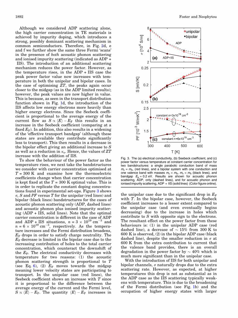
To show the behaviour of the power factor as thetemperature rises, we next take the bandstructureswe consider with carrier concentration optimised atT = 300 K and examine how the thermoelectriccoefficients change when that carrier concentrationis kept fixed at the T = 300 K optimal value. This isin order to replicate the constant doping concentra-tions found in experimental set-ups. Figure 3 showsr, S and PF versus T for the unipolar (red lines) andbipolar (black lines) bandstructures for the cases ofacoustic phonon scattering only (ADP, dashed lines)and acoustic phonon plus ionised impurity scatter-ing (ADP + IIS, solid lines). Note that the optimalcarrier concentration is different in the case of ADPand ADP + IIS situations, n = 3 9 1019 cm�3 andn = 6 9 1019 cm�3, respectively. As the tempera-ture increases and the Fermi distribution broadens,EF drops in order to satisfy charge neutrality. TheEF decrease is limited in the bipolar case due to theincreasing contribution of holes to the total carrierconcentration, which counteract the downshift ofthe EF. The electrical conductivity decreases withtemperature for two reasons: (1) the acousticphonon scattering strength is proportional to T(see Eq. 6), (2) EF moves towards the midgapmeaning lower velocity states are participating totransport. In the unipolar case (red lines), theSeebeck coefficient shows an increase with T sinceit is proportional to the difference between theaverage energy of the current and the Fermi level,S / Eh i � EF. The quantity Eh i � EF increases in
the unipolar case due to the significant drop in EF
with T. In the bipolar case, however, the Seebeckcoefficient increases to a lesser extent compared tothe unipolar case (and even eventually beginsdecreasing) due to the increase in holes whichcontribute to S with opposite sign to the electrons.The resultant effect on the power factor from thesebehaviours is: (1) in the unipolar ADP case (reddashed line), a decrease of � 15% from 300 K to600 K is observed, (2) in the bipolar ADP case (blackdashed line), despite the smaller reduction in r at600 K from the extra contribution to current thatthe valence band provides, there is an overalldegradation in the power factor by � 40% which ismuch more significant than in the unipolar case.
With the introduction of IIS for both unipolar andbipolar channels, r naturally drops due to the extrascattering rate. However, as expected, at highertemperatures this drop is not as substantial as inthe ADP case as the IIS scattering typically weak-ens with temperature. This is due to the broadeningof the Fermi distribution (see Fig. 1b) and theoccupation of higher energy states with larger
Fig. 3. The (a) electrical conductivity, (b) Seebeck coefficient, and (c)power factor versus temperature at constant carrier concentration fortwo bandstructures: a single parabolic conduction band of massmc = m0, (red lines), and a bipolar system with one conduction andone valence band with masses mc = m0, mv = m0 (black lines), andbandgap Eg = 0.2 eV. Results are shown for acoustic phononscattering, ADP, only (dashed lines), and for acoustic phonon andionised impurity scattering, ADP + IIS (solid lines) (Color figure online).
Foster and Neophytou1892

wavevectors which are less impacted by IIS. Thiscan again be seen from the IIS stronger impact onthe transport distribution function at lower energiesin Fig. 1d. The improvement in r from the valenceband contribution in the ADP case in the bipolarchannel (comparing red-dashed to black-dashedlines in Fig. 3a) is now also missing in the ADP +IIS lines due to the widening of the ‘effective
transport bandgap’ that IIS causes as explainedearlier, and effectively makes the material ‘look’more unipolar (Fig. 1d).
When it comes to the Seebeck coefficient inFig. 3b and the introduction of IIS, bipolar trans-port no longer has such a strong effect on S withincreasing temperatures, due to this widening of the‘effective transport bandgap’ due to IIS, unlike inthe ADP-limited case (black-solid versus black-dashed line in Fig. 3b). The result of these effectson the PF, therefore, is a significant reduction at lowtemperatures compared to the ADP-limited case,but an increase with temperature (Fig. 3c). Theincrease is a consequence of the smaller relativereduction in r and the continuous rising of S.
Figure 3 shows and explains why the power factordrops (in the ADP case) or increases less that itsoptimal value if the carrier concentration (con-trolled by doping) remains at the T = 300 K optimallevels. We now show that the power factor can beimproved by a careful optimisation of the carrierconcentration at higher temperature operations. InFig. 4a we show the optimal PF of the unipolar (redlines) and bipolar (black lines) bandstructures forthe cases of ADP scattering only (dashed lines) andADP + IIS (solid lines), i.e., the peaks of the Fermiscans seen in Fig. 2.
For ADP scattering only, whereas the unipolarsystem previously saw a reduction of � 15%, byoptimising the doping with temperature the powerfactor now remains constant (Fig. 4a—red-dashedline). In the bipolar case the dramatic fall in thepower factor due to the Seebeck reduction (as seenpreviously in Fig. 3b, black-dashed line) is miti-gated by increasing the Fermi level. Consequentlythe power factor, although still slightly decreasingwith temperature, is now � 60% higher at 600 Kthan in the un-optimised case from Fig. 3c (un-optimised values from Fig. 3c shown by the squaremarkers at 600 K in red (unipolar) and black(bipolar).
The Fermi level required to produce these optimalvalues rises linearly with temperature in the unipo-lar system (red-dashed line in Fig. 4b). This beha-viour was earlier identified by Ioffe in Ref. 9 whereit was shown that the optimal reduced Fermi levelgF,opt = (EF � EC)/kBT = r, where r is an exponentthat depends on the electron scattering mechanism.Since r is a constant, this gives EF / T. In our caseof acoustic phonon scattering r = 0, so we wouldexpect the power factor to peak at the band edge.However, Ioffe’s derivation assumes Boltzmannstatistics for the carrier distribution and, indeed,
running our calculations under that assumptionreproduces such a result (not shown). However,using the more accurate (for degenerate dopingconditions) Fermi–Dirac distribution, we find thatin the case of acoustic phonon scattering gF,opt � 2/3.In the bipolar system the linear behaviour seen inthe unipolar case no longer holds, and the optimumFermi level rises quicker than linearly (black-dashed line in Fig. 3b). This is in order to avoidthe detrimental impact of the bipolar effect that thevalence band introduces.
In Fig. 4c we also show the optimal carrierconcentration required to set EF at the optimalposition. As has been previously identified in theliterature,9,21 the optimal carrier concentration in aunipolar system increases as nopt / T3=2 (red-dashed line). Again, however, in the bipolar system(black-dashed line) the unipolar behaviour nolonger holds, and the required carrier concentrationrises more quickly in order to produce the higherFermi levels seen in Fig. 4b, following an
Fig. 4. The optimal values of (a) the power factor, (b) Fermi level, and(c) carrier concentration versus temperature for two bandstructures: asingle parabolic conduction band of mass mc = m0, (red lines), and abipolar systemwithoneconductionandonevalencebandwithmassesmc = m0,mv = m0 (black lines), andbandgapEg = 0.2 eV.Resultsareshown for acousticphononscatteringonly,ADP (dashed lines), and foracoustic phonon and ionised impurity scattering, ADP + IIS (solidlines) (Color figure online).
Doping Optimization for the Power Factor of Bipolar Thermoelectric Materials 1893

approximate T1:8 trend. Indeed, at T = 600 K theoptimal bipolar carrier concentration is 30% higherthan the optimal unipolar carrier concentration.
When IIS is included, the power factor values arelower as explained previously, but increase withincreasing temperature due to the occupation ofhigher energy states which scatter less under IIS.Benefits compared to the un-optimised values (dia-mond markers in Fig. 4a) are not as great as in theADP only case, but still significant—10% for theunipolar bandstructure and 20% for the bipolarbandstructure (solid lines in Fig. 4a). The Fermilevel and carrier concentration values needed toachieve these power factor values are higher than inthe ADP only case. For practical purposes, there-fore, to achieve an optimized power factor in thebipolar case at T = 600 K in the material weconsider of bandgap Eg = 0.2 eV, the doping con-centration needs to be by 160% higher compared tothe value that provides optimized PF at T = 300 K.That value is by 10% higher compared to the onethat achieves the optimal T = 600 K PF in theunipolar case. Note that in the case of the ADP +IIS transport conditions, the optimal doping den-
sity is higher, due again to the widening of the‘effective transport bandgap’ seen in Fig. 1d. Alsonote that these values are to be altered in the case ofa different bandgap, i.e., the relevance of thesevalues are shifted to lower/higher temperatures asthe bandgap decreases/increases.
Finally, due to the influence of the thermalconductivity in the denominator of ZT, which hasits own temperature dependence, ZT does not peak
at the same EF or carrier concentration as the PF.Therefore, in Fig. 5 we compare the optimal carrierconcentration and Fermi levels when optimising forthe power factor (same black lines as in Fig. 4b andc) and optimising for ZT (green lines). This compar-ison here is shown only for the bipolar materialsince the unipolar material does not show a peak asexplained previously. For the calculation of ZT weconsider only the electronic properties (i.e., we takejl= 0, as the behaviour of jl is material dependentand more complex). Since je / r through the Lorenznumber, je is reduced with falling EF and, therefore,the peaks in ZT occur at significantly lower densityand EF than when just optimising for the PF. As thetemperature is increased, however, the optimalvalues (in both ADP and ADP + IIS cases) rise ata quicker pace than when optimising for PF. This isbecause as the temperature increases the impact ofthe bipolar effect kicks in and jbi increasinglypushes the peak away from the midgap. The intro-duction of IIS, however, when optimising for ZT hasmuch less influence than in when optimising for thePF. This is again due to je being proportional to r. Ascan be seen in Fig. 3, the introduction of IIS primarilyaffects r. When optimising for ZT, this impact is thencancelled out by the same impact on je.
Of course in a real material jl 6¼ 0 and the optimalZT values will lie somewhere between the PF-optimised and our jl= 0 ZT-optimised values. Inparticular, it is interesting to note that the smallerthe value of jl in the material with respect to the je,the closer it is to the jl= 0 ZT-optimised case, and,therefore, the less it needs to be doped to reach itsoptimal ZT, which can prove helpful for TE mate-rials, as doping at extremely high values can provedifficult in many cases.
Finally, we would like to state that in this workwe employed a simple two-band parabolic model toobtain first order optimization strategies for dopingin bipolar TE materials. In reality, material band-structures are typically more complex than thesimple two-band parabolic model we assume here.Real material bandstructures can have a variety ofband gaps, effective masses, band degeneracies,band non-parabolicity, and multiple valence and/orconduction bands. Many of these bandstructurefeatures can also vary with temperature, anddetailed studies on each material are essential forproper optimization. In this study, however, it wasour aim to demonstrate to first order the important,yet overlooked, impact of the bipolar effect on thedoping optimisation.
CONCLUSIONS
Using the Boltzmann transport formalism wehave calculated the thermoelectric transport coeffi-cients for unipolar and bipolar systems and pre-sented a study on the optimal doping conditions forthe power factor and ZT figure of merit. We haveshown that, if the carrier concentration is not
Fig. 5. The optimal values of (a) carrier concentration and (b) theFermi level versus temperature for a bipolar bandstructure tomaximise the power factor (black lines) and ZT (green lines) in thecase of acoustic phonon scattering only, ADP (dashed lines) andacoustic phonon and ionised impurity scattering, ADP + IIS (solidlines) (Color figure online).
Foster and Neophytou1894

properly optimised at the temperature of operation,but room temperature optimal doping is consid-ered, the power factor can underperform by 15% inthe unipolar systems, and 40% in the bipolarsystem under ADP scattering, and 10% in theunipolar systems, and 20% in the bipolar systemunder ADP + IIS scattering. Consequently, signifi-cant enhancements in the PF (� 40%) can beachieved through doping optimisation. Furthermorewe have identified that in a bipolar system theoptimal carrier concentration indicates an approxi-mately T1:8 trend, larger compared to the T3=2 trendin unipolar materials, a result of the additionaldegradation due to bipolar transport. In our simula-tions, the optimal carrier concentration at T = 600 Kin a material with bandgap Eg = 0.2 eV (e.g., approx-imately that of Bi2Te3) then becomes 30% larger thanexpected from the unipolar calculation. We believethat our findings will be useful in the optimal designof bipolar thermoelectric materials.
ACKNOWLEDGMENTS
This work has received funding from the Euro-pean Research Council (ERC) under the EuropeanUnion’s Horizon 2020 Research and InnovationProgramme (Grant Agreement No. 678763).
OPEN ACCESS
This article is distributed under the terms of theCreative Commons Attribution 4.0 InternationalLicense (http://creativecommons.org/licenses/by/4.0/),which permits unrestricted use, distribution, andreproduction in any medium, provided you giveappropriate credit to the original author(s) and thesource, provide a link to the Creative Commonslicense, and indicate if changes were made.
REFERENCES
1. G. Prashun, S. Vladan, and E.S. Toberer, Nat. Rev. Mater. 2,17053 (2017).
2. L.-D. Zhao, H.J. Wu, S.Q. Hao, C.I. Wu, X.Y. Zhou, K. Bis-was, J.Q. He, T.P. Hogan, C. Uher, C. Wolverton, V.P.Dravid, and M.G. Kanatzidis, Energy Environ. Sci. 6, 3346(2013).
3. H. Goldsmid, Materials 7, 2577 (2014).4. L.-D. Zhao, V.P. Dravid, and M.G. Kanatzidis, Energy
Environ. Sci. 7, 251 (2014).5. M. Lundstrom,Notes onBipolar Thermal Conductivity (2017).
https://nanohub.org/groups/ece656_f17/File:Notes_on_Bipolar_Thermal_Conductivity.pdf. Accessed 11 June 2018.
6. M. Thesberg, H. Kosina, and N. Neophytou, Phys. Rev. B 95,125206 (2017).
7. G. Snyder and E. Toberer, Nat. Mater. 7, 105 (2008).8. Q. Zhang, Q. Song, X. Wang, J. Sun, Q. Zhu, K. Dahal, X.
Lin, F. Cao, J. Zhou, S. Chen, G. Chen, J. Mao, and Z. Ren,Energy Environ. Sci. 11, 933 (2018).
9. A.F. Ioffe, Semiconductor Thermoelements, and Thermo-electric Cooling (London: Infosearch Ltd., 1957).
10. P.G. Burke, B.M. Curtin, J.E. Bowers, and A.C. Gossard,Nano Energy 12, 735 (2015).
11. J.-H. Bahk and A. Shakouri, Phy. Rev. B 93, 165209 (2016).12. H.-S. Kim, K.H. Lee, J. Yoo, W.H. Shin, J.W. Roh, J.-Y.
Hwang, S.W. Kim, and S.I. Kim, J. Alloys Compd 741, 869(2018).
13. L. Zhang, P. Xiao, L. Shi, G. Henkelman, J.B. Goodenough,and J. Zhou, J. Appl. Phys. 117, 155103 (2015).
14. B. Poudel, Q. Hao, Y. Ma, Y. Lan, A. Minnich, B. Yu, X. Yan,D. Wang, A. Muto, D. Vashaee, X. Chen, J. Liu, M.S.Dresselhaus, G. Chen, and Z. Ren, Science 320, 634 (2008).
15. G. Mahan and J.O. Sofo, Proc. Natl. Acad. Sci. USA 93, 7436(1996).
16. T.J. Scheidemantel, C.A. Draxl, T. Thonhauser, J.V. Bad-ding, and J.O. Sofo, Phys. Rev. B 68, 125210 (2003).
17. M. Lundstrom, Fundamentals of Carrier Transport (Cam-bridge: Cambridge University Press, 2000).
18. S. Foster, M. Thesberg, and N. Neophytou, Phys. Rev. B 96,195425 (2017).
19. N. Neophytou and M. Thesberg, J. Comput. Electron. 15, 16(2016).
20. C. Jeong, R. Kim, and M. Lundstrom, J. Appl. Phys. 111,113707 (2012).
21. G. Tan, L.-D. Zhao, and M. Kanatzidis, Chem. Rev. 116,12123 (2016).
Doping Optimization for the Power Factor of Bipolar Thermoelectric Materials 1895