download the full article - college of intensive care medicine
TRANSCRIPT
Int. J. Electrochem. Sci., 8 (2013) 7634 - 7645
International Journal of
ELECTROCHEMICAL SCIENCE
www.electrochemsci.org
Fabrication of High-Efficiency Silicon Solar Cells by Ion
Implant Process
Chien-Ming Lee, Sheng-Po Chang*, Shoou-Jinn Chang, Ching-In Wu
Institute of Microelectronics & Department of Electrical Engineering, Center forMicro/Nano Science
and Technology, Advanced Optoelectronic Technology Center, National Cheng Kung University,
Tainan 70101, Taiwan *E-mail: [email protected]
Received: 18 April 2013 / Accepted: 16 May 2013 / Published: 1 June 2013
This paper presents a novel method to produce high-efficiency silicon solar cells via an ion-implanted
procedure. The proposed method simplifies the conventional thermal POCl3 diffusion process by
eliminating two production stages: phosphosilicate glass (PSG) removal, and junction isolation. The
PC-1D computer program was used in two-diode mode to simulate the performance of the implant
process, and a cell tester with Berger flash system was used to measure I-V. Higher Voc was achieved
because of good surface passivation, caused by the ion implanted and annealing processes. The
proposed ion implanted method achieved 18.77% efficiency when applied to 156 × 156 mm p-type Cz
wafers.
Keywords: Ion Implant, PSG, POCl3, Solar Cell
1. INTRODUCTION
In recent years, government policies have provided incentives to increase demand and stimulate
the photovoltaics (PV) industry, and the solar energy market has therefore experienced explosive
growth. However, the cost of photovoltaic electricity is presently higher than that of grid electricity.
Reduced manufacturing costs and greater cell efficiency are very important in achieving grid parity.
Reducing silicon bulk thickness is one solution to lowering manufacturing cost. This will increase the
amount of wafer obtained per ingot or brick, and reduce the cost per watt of photovoltaic energy.
However, this approach could suffer wafer-handling issues, and the trade-off is a higher rate of wafer
breakage during cell and module processes. It is obvious that improved solar cell efficiency is very
important in the future, and may achieve remarkable leverage of costs within the solar chain. Many

Int. J. Electrochem. Sci., Vol. 8, 2013
7635
methods have been proposed to improve solar-cell efficiency, including metal wrap through (MWT)
solar cell [1,2], emitter wrap through (EWT) cells [3,4], interdigitated backside contact (IBC) cells
[5,6], laser-fired contacts cells [7,8], and ion-implanted cells [9,10]. Of these methods, ion
implantation is an attractive and cost-effective process.
Commercialized silicon solar cell technologies presently use thermal POCl3 diffusion to realize
the p-n junction and build-in voltage. During thermal diffusion, phosphosilicate glass (PSG) is
generated on the surface as a result of the reaction between phosphorous and oxygen. After the
diffusion process, a wet chemical process is used to remove the PSG layer. There are two ways to
isolate parasitic junctions: One is wet isolation combined with a PSG cleaning step; the other is laser
isolation. These two isolation processes reduce the wafer area, especially the laser method, which can
damage the wafer surface.
The ion implant process has many advantages over the conventional process. (1) The process
enables precise control of the dose, making it possible to perform single-side p-n junction and
eliminate the isolation process; this would also help achieve very good Rsheet uniformity (<3%), and
the lightly doped modules would absorb more sunlight. (2) The independent control of impurity depth
and dose allows the adjustment of the doping profile and concentration. (3) The ion-implant process
helps fabricate defect-free products; unlike in the method involving POCl3 thermal diffusion, no dead
layer or glass byproduct appear on the surface. Further, an annealing stage was added to realize a good
passivation surface. (4) The ion-implant process also helps realize high throughput; it is possible to
produce at least 1000 pieces/h. However, the process also has drawbacks. For example, (1) it cannot be
applied for very deep or very shallow junctions; (2) it cannot be implemented on poly wafers; and (3)
toxic gases such as phosphine (PH3) and arsine (AsH3) are generated during the process.
2. EXPERIMENT
Figure 1. The process flowchart for conventional and ion-implanted solar cell production

Int. J. Electrochem. Sci., Vol. 8, 2013
7636
Monocrystalline Czochralski silicon wafers (CZ-Si) with resistivites of 0.5–3 Ω cm, thickness
180–200 μm, and pseudo square-shaped dimensions 156 mm × 156 mm were used. Figure 1 compares
the process flow of the conventional thermal POCl3 diffusion and the ion-implanted methods. First, the
damage caused by the wire saw during wafer-slicing was repaired. Wafers were dipped in high-
concentration KOH solution 5.04 wt% without IPA solution to remove saw-damage. Then, anisotropic
etching with volume ratio KOH:IPA:H2O = 1:1.6:34 produces 3–5 μm pyramids on the surface to
reduce reflection. The next step for the commercial process is the thermal POCl3 diffusion to form the
emitter. The wafers are placed vertically into a quartz wafer carrier (quartz boat) and then the carrier
moves into a quartz and is heated to 840°C. The dopant gas reacts with silicon at the surface in the
presence of O2 at high temperature. The following reactions take place:
Si+O2SiO2 (1)
POCl3+O2P2O5 +Cl2 (2)
In the implant process, the ion dopant bombards the wafer surface and subsequently penetrates
the wafer. This bombardment results in crystal damage, which can be recovered by high-temperature
annealing. In this paper, PH3 gas was used as a P+ ion source with low beam energy (10 keV) and a
dose of 3.0E15 P+/cm
2 was implanted on the surface. A furnace tube was then used for thermal
annealing. In the annealing step, dry oxide is used to activate the dopant and fabricate the junction.
After annealing, the dopant concentration profile is different from POCl3 [11–14]. The doping
concentration profile of POCl3 ranges from erfc to Gaussian distribution in which peak dopant occurs
at the surface. By contrast, the profile of ion implantation occurs at a specific depth below the surface.
The detailed profile can be seen in Ref [11–14].
After annealing, the SiNx layer was followed to be anti-reflection coating (ARC). The silicon
nitride thickness of the implant process is thinner than that of the conventional POCl3 process. After
ARC, the metal contact was fulfilled by screen printing and co-firing. For the screen printing, the
front-side silver (Ag) paste is Heraus 9411 and the pattern design has 3 busbars, and 78 finger lines.
Backside Aluminum (Al) is Monocrystal RX-1203 and backside silver (Ag) is DuPont PV-157. The
isolation process is not needed for the implant process. Finally, the extraction of the basic parameter
and IV curves of cells are measured at 25°C and AM 1.5G on single-pulse sun simulators from Berger
Lichttechnik. The standard parameter set Voc, Isc, and FF, the shunt resistance Rsh is determined by
the linear slope of the reverse dark current on every cell. The series resistance Rs is calculated from
two IV curves measured at 1000 W/m2 and 500 W/m
2 according to IEC 891.
3. RESULTS AND DISCUSSION
Four different peak temperatures (810, 840, 870 and 900°C) were used during the annealing
step in the ion implantation process. Table 1 compares Rsheet uniformity between POCl3 diffusion and
4 different annealing processes. As seen from the data, Rsheet decreases when the peak temperature
increases from 810°C to 900°C. We also found that the Rsheet uniformity of thermal POCl3 diffusion
was worse than that of the implant process. The better uniformity of the implant process was due to
precise dosage control in the emitter by the ion implant tool. After implantation, a thermal annealing

Int. J. Electrochem. Sci., Vol. 8, 2013
7637
step is needed to activate the phosphorous. The high Rsheet uniformity and precise control also enable
a repeatable process for fabrication of lightly doped emitter regions [15–17].
Table 1. Comparison of Rsheet uniformity between POCl3 diffusion and different annealing processes.
Rsheet [Ω/sq] Ave MAX MIN Uniformity
POCl3 65.68 68.89 62.38 4.96%
Anneal 810 69.73 72.01 68.32 2.65%
Anneal 840 63.75 65.60 62.38 2.53%
Anneal 870 61.27 62.97 59.44 2.88%
Anneal 900 57.33 59.01 56.04 2.59%
In order to achieve the best electrical characteristics in the annealing step, wafer surfaces with
double-sided implant dopant 2.0E15 and beam energy 10 keV were used to be monitor implied Voc
[18] to determine which was the most appropriate annealing temperature.
0.62
0
0.62
2
0.62
4
0.62
6
0.62
8
0.63
0
0.63
2
0.63
4
0.63
6
0.63
8
0.64
0
0.64
2
0.64
4
0.64
6
0.1
1
10
0.6380.6360.6330.631
Inte
nsi
ty(S
un
s)
Implied Voc (v)
POCl3
Anneal900
Anneal870
Anneal840
Anneal810
0.628
Figure 2. Implied Voc of POCl3 and the implant process with a passivated double-sided layer
Table 2. Implied Voc and lifetime.
POCl3 Anneal
900
Anneal
870
Anneal
840
Anneal
810
Implied Voc
(V)
0.628 0.631 0.633 0.638 0.636
Lifetime (μs) 41.5 45.7 48.3 52.1 51.7

Int. J. Electrochem. Sci., Vol. 8, 2013
7638
A silicon wafer lifetime tester (WCT-120) was used to measure implied Voc (Fig. 2) and
lifetime (Table 2); details of the measurement formula are given in Ref [19]. The results show that the
implied Voc of thermal POCl3 diffusion was 0.628 V at 1 sun, which is worse than the implant
process. The implied Voc of high-temperature annealing at 900°C was 0.631 V, which is worse than
the implant process. This is due to high temperature, which will degrade the lifetime and cause lower
Voc. The best implied Voc result was achieved by annealing at 840°C, and this condition was
subsequently used to ensure the highest performance.
Table 3. Measure the thickness of the SiO2 layer..
POCl3 Anneal
900
Anneal
870
Anneal
840
Anneal
810
SiO2 thickness (nm) x 16.91 16.56 16.17 15.98
Uniformity (%) x 0.78% 0.98% 0.91% 1.12%
After annealing, thinner oxide layer was formed on the wafer surface. In order to determine the
thickness of the SiO2 layer, <111> silicon polish wafer with a dose of 3.2E15 on the surface was used
as the monitor wafer.
200 400 600 800 1000 1200
0
10
20
30
40
50
60
Refl
ecti
on
(%)
Wavelength(nm)
POCl3
Implant
Figure 3. Surface reflection of POCl3 and implant wafers after SiNX deposition
A single-wavelength (632.8 nm) He–Ne laser was shot onto the wafer surface to measure the
refractive index and thickness of the dielectric layer. Table 3 shows that, after annealing, the SiO2
thickness was around 16 nm, and that the results are very consistent. According to the thinner oxide
layer on the surface, the thickness of the silicon nitride should be modulated. In order to minimize
reflection from the front-side of the cell, a 57-nm SiNx layer was deposited on top of the SiO2. In the
short-wavelength range, the POCl3 process produced less reflection than the implant process after
Int. J. Electrochem. Sci., Vol. 8, 2013
7639
deposition of ARC (see Fig. 3). According to the Schustter diagram [20], the optimum refractive index
of the inner n1 layer and outer layer n2 on silicon substrate are calculated as below for zero reflection:
AB/CD>0
Where
A=no-ns, B=non22 – ns n1
2
C=nons-n22, D=n1
2 – ns n0
According to the calculation [20], better optical performance is based on the design of low–
high (outer layer–inner layer) refractive index on silicon substrate. However, in the implant process,
the design of ARC is opposite, where the outer layer is SiNx (refractive index 2.03) and the inner layer
is SiO2 (refractive index 1.46). In the long-wavelength range, the reflection from the implant process
was lower than that of the POCl3 process. This is because the wafer has a planer backside surface
caused by wet chemical isolation, which uses HNO3 and HF to remove the backside p-n junction
following the POCl3 diffusion process.
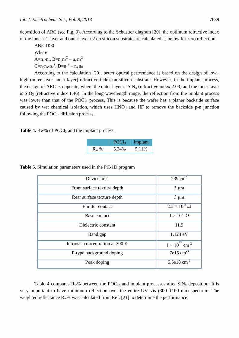
Table 4. Rw% of POCl3 and the implant process.
POCl3 Implant
Rw % 5.34% 5.11%
Table 5. Simulation parameters used in the PC-1D program
Device area 239 cm2
Front surface texture depth 3 μm
Rear surface texture depth 3 μm
Emitter contact 2.5 × 10⁻³ Ω
Base contact 1 × 10⁻³ Ω
Dielectric constant 11.9
Band gap 1.124 eV
Intrinsic concentration at 300 K 1 × 1010 cm-3
P-type background doping 7e15 cm-3
Peak doping 5.5e18 cm-3
Table 4 compares Rw% between the POCl3 and implant processes after SiNx deposition. It is
very important to have minimum reflection over the entire UV–vis (300–1100 nm) spectrum. The
weighted reflectance Rw% was calculated from Ref. [21] to determine the performance:

Int. J. Electrochem. Sci., Vol. 8, 2013
7640
Rw%=
where Fi(λ) is photon flux, and Qi(λ) is cell internal quantum efficiency [22,23]. Table 4 shows
that the Rw% of the implant process was 5.11%, which is better than the POCl3 process (5.34%) after
ARC.
To validate the model, we compare the experimental result via the PC-1D simulation program
[24]. Fig. 4 shows a schematic design of the device, and Table 5 shows the values of the main cell
parameters in the PC-1D simulation. Fig. 5 shows the simulation result for the relationship between
Voc, and thickness of SiNX and SiO2. Maximum Voc reached 0.642 V at SiNX 56.55 nm and SiO2
16.48 nm. Figs. 6 and 7 also examined the same relationship and found the same trend. The maximum
Isc and efficiency was 8.92 A and 18.92% at SiNX 56.55 nm and SiO2 16.48 nm.
After ARC, batches (400 pieces per batch) were produced using a screen-printing process. Fig
8 compares Voc and Isc between the POCl3 and implant processes, and shows that Voc was lower for
the POCl3 process than that of the implant process, because the carrier lifetime achieved using the
implant process is superior to that of the POCl3 process.
Figure 4. Schematic design of the device in PC-1D simulation
This same result is confirmed in Table 2. Good agreement was observed with the results of Ref
[17]. For the implant process, there is no dead layer in the near surface. As a result, the surface
recombination of the implant process is lower than that of the POCl3 process, which produces higher
Voc and Isc than the POCl3 process. The Voc of the higher temperature 900°C annealing step was less
than that achieved at 840°C, confirming that high annealing temperature causes lifetime degradation.

Int. J. Electrochem. Sci., Vol. 8, 2013
7641
According to the heavy doping caused by high-temperature annealing, the Isc at high temperature is
lower than that of the low-temperature process.
020
4060
80100
0.632
0.634
0.636
0.638
0.640
0.642
0
510
1520
2530
Vo
c (
V)
SiO 2 (n
m)
SiNX (nm)
Figure 5. Simulation of relationship between Voc, SiNX, and SiO2
020
4060
80100
6.5
7.0
7.5
8.0
8.5
9.0
05
1015
2025
30
Isc(A
)
SiO2 (n
m)
SiNX (nm)
Figure 6. Simulation of the relationship between Isc, SiNX, and SiO2

Int. J. Electrochem. Sci., Vol. 8, 2013
7642
020
4060
80100
13.514.0
14.5
15.0
15.5
16.0
16.5
17.0
17.5
18.0
18.5
19.0
05
1015
2025
30
Eff
icie
ncy
(%)
SiO2
(nm
)SiN
X(nm)
Figure 7. Simulation of the efficiency in relation to SiNX and SiO2
POC
l3
Annea
l-810
Annea
l-840
Annea
l-870
Annea
l-900
0.627
0.628
0.629
0.630
0.631
0.632
0.633
0.634
Voc
Isc
Process
Vo
c (
V)
8.78
8.80
8.82
8.84
8.86
8.88
8.90
8.92
Isc (A
)
Figure 8. Voc and Isc of POCl3 and the implant process

Int. J. Electrochem. Sci., Vol. 8, 2013
7643
POC
l3
Annea
l-810
Annea
l-840
Annea
l-870
Annea
l-900
2.2
2.4
2.6
2.8
3.0
3.2
3.4
Rs
FF
Process
Rs
(mo
hm
)
78.2
78.4
78.6
78.8
79.0
79.2
79.4
79.6
79.8
80.0
FF
(%)
Figure 9. Rs and FF of POCl3 and the implant process
POC
l3
Annea
l-810
Annea
l-840
Annea
l-870
Annea
l-900
18.2
18.3
18.4
18.5
18.6
18.7
18.8
Eff
icie
ncy
(%
)
Process
Efficiency
Figure 10. Efficiency of POCl3 and the implant process

Int. J. Electrochem. Sci., Vol. 8, 2013
7644
In Figure 9, The Rs of the implant process is lower than that of the POCl3 process, due to good
Rsheet uniformity caused by precise doping control by the implant tool. For the different annealing
temperatures, higher temperature produces heavy doping, which ensures good contact with metal.
Figure 10 shows that the highest average efficiency is 18.77%, achieved with the implant process and
annealing at 840°C. All of the electrical characteristics of the samples are shown in Table 6, indicating
that the efficiency of the implant process is higher than that of POCl3. Higher efficiency is due to
higher Voc. These results are consistent with those of the PC-1D simulation program.
Table 6. Characteristics of POCl3 and the implant process
Item Uoc
(V)
Isc (A) Rs (mΩ) Rsh (Ω) FF (%) Ncell
(%)
Irev1(A)
POCl3 0.627 8.88 3.39 476.94 78.25 18.23 0.05
Anneal-810 0.633 8.91 2.42 44.08 79.11 18.68 0.52
Anneal-840 0.634 8.90 2.41 39.92 79.47 18.77 0.64
Anneal-870 0.631 8.88 2.33 48.07 79.20 18.58 0.46
Anneal-900 0.631 8.80 2.33 28.68 79.40 18.44 0.59
4. CONCLUSION
This study investigated a novel production method of ion-implanted emitter formation for high-
efficiency silicon photovoltaic cells. This innovation increased absolute cell efficiency by 0.5% on
solar CZ grade wafer, and enabled a simplified process flow by eliminating the need for the PSG strip
and junction isolation stages. Due to precise dopant control by the ion implant tool, the Rsheet
uniformity of the implant process is greater than that of thermal POCl3 diffusion. After annealing, the
implied Voc of the implant process is better than that of the POCl3 process, due to good surface
passivation caused by the implant and annealing processes. However, thinner SiO2 formed on the
surface by annealing process, and so the thickness of the silicon nitride should be modified to
minimized Rw%. Simulation program, PC-1D, is used to validate the model and is in accordance with
the results. After metallization, average cell efficiency of 18.77% was achieved.
ACKNOWLEDGMENTS
The authors would like to thank the National Science Council and Bureau of Energy, Ministry of
Economic Affairs of Taiwan, R.O.C. for the financial support under Contract No. 101-2221-E-006-139
and 101-D0204-6 and the LED Lighting Research Center of NCKU for the assistance of device
characterization. This work was also supported in part by the Center for Frontier Materials and
Micro/Nano Science and Technology, the National Cheng Kung University, Taiwan. This work was
also supported in part by the Advanced Optoelectronic Technology Center, the National Cheng Kung
University, under projects from the Ministry of Education.

Int. J. Electrochem. Sci., Vol. 8, 2013
7645
References
1. E. Lohmuller, B. Thaidigsmann, M. Pospischil, U. Jager, S. Mack, J. Specht, J. Nekarda, M.
Retzlaff, A. Krieg, F. Clement, A. Wolf, D. Biro, IEEE Electron Device Lett., 32 (2011) 1719.
2. B. Thaidigsmann, A. Drews, T. Fellmeth, P. Saint-Cast, A. Wolf, F. Clement, R.Preu, D. Biro,
IEEE J. Photovolt., 2 (2012) 109.
3. F. Kiefer, C. Ulzhöfer, T. Brendemühl, N.-P. Harder, R. Brendel, V. Mertens, S. Bordihn, C. Peters,
JW. Müller, IEEE J. Photovolt., 1 (2011) 49.
4. D. Kray, J. Dicker, D. Osswald, A. Leimenstoll, S.W. Glunz, W. Zimmermann, K.-H. Tentscher,
G. Strobl, 3rd WCPEC., (2003) 11.
5. J. Renshaw, A. Rohatgi, 37th IEEE PVSC., (2011) 2924.
6. F. J. Castano, D. Morecroft, M. Cascant, H. Yuste, M. W. P. E. Lamers, A. A. Mewe, I. G. Romijn,
E. E. Bende, Y. Komatsu, A. W. Weeber, I. Cesar, 37th IEEE PVSC., (2011) 1038.
7. T. Boscke, R. Hellriegel, T. Wutherich, L. Bornschein, A. Helbig, R. Carl, M. Dupke, D.
Stichtenoth, T. Aichele, R. Jesswein, T. Roth, C. Schollhorn, T. Geppert, A. Grohe, J. Lossen, H.-J.
Krokoszinski, 37th IEEE PVSC., (2011) 3663.
8. P. Ortega, G. Lopez, A. Orpella, I. Martin, M. Colina, C. Voz, S. Bermejo, J. Puigdollers, M.
Garcia, R. Alcubilla, 8th Spanish CDE' (2011) 1.
9. M. Jeon, J. Lee, S. Kim, W. Lee, E. Cho. Mater. Sci. Eng., B., 176(2011)1285.
10. T. Janssens, N.E. Posthuma, B.J. Pawlak, E. Rosseel, J. Poortmans, 25th EUPVSEC , (2010) 1179.
11. H.F. Wolf, Semiconductors, John Wiley & Sons Inc., New York (1971).
12. AS. Grove, Physics and Technology of Semiconductor Devices, John Wiley & Sons Inc., (1967).
13. DV. Morgan, K. Board, RH. Cockrum, An introduction to Microelectronic Technology, John
Wiley & Sons Inc., (1985).
14. S.M. Sze, Semiconductor Device Physics and Technology, John Wiley& Sons Inc, (1969).
15. R. Low, A. Gupta, H.-J. Gossmann, J. Mullin, V. Yelundur, B. Damiani, V. Chandrasekaran, D.
Meier, B. McPherson, A. Rohatgi, 35th EUPVSEC, (2010)1440.
16. J. Benick, N. Bateman, M. Hermle, 25th EUPVSEC, (2010)1169.
17. T. Janssens, N.E. Posthuma, B.J. Pawlak, E. Rosseel, J. Poortmans, 25th EUPVSEC, (2010)1179.
18. R. A. Sinton, A. Cuevas, M. Stuckings, 25th IEEE PVSC., (1996) 457.
19. R. A. Sinton, A. Cuevasa, Appl. Phys. Lett.,69 (1969) 2510.
20. B. A. Moys, Thin Solid Films.,21 (1974) 145.
21. D. Redfield, Sol. Energy Mater. Sol. Cells.,3 (1981) 27.
22. G. E. Jellison, F. A. Modine, J. Appl. Phys.,53 (1982) 3745.
23. E. D. Palik, Handbook of optical constants of solids. Academic Press, New York, (1985).
24. P. A. Basore, D. T. Rover, A. W. Smith, Twentieth IEEE Photovoltaic Specialists
Conference.,1(1988) 389.
© 2013 by ESG (www.electrochemsci.org)