1
3 MEMS FABRICATION
•Ken Gilleo PhD•ET-Trends LLC
24%
2
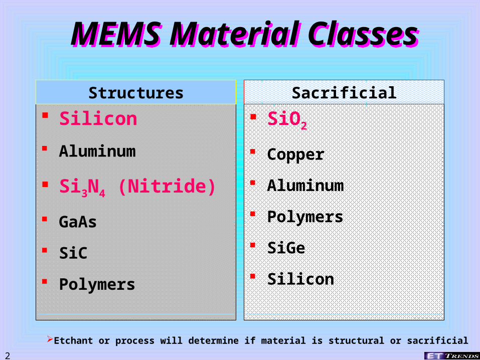
MEMS Material Classes
MEMS Material Classes
Silicon
Aluminum
Si3N4 (Nitride)
GaAs
SiC
Polymers
SiO2
Copper
Aluminum
Polymers
SiGe
Silicon
Structures Sacrificial
Etchant or process will determine if material is structural or sacrificial

3
Movable StructuresMovable
Structures Pivots Bearings Hinges Beams (bend/twist) Gears Rack Wheels Latch Switches Valves Diaphragms Turbines Springs

4
Stationary StructuresStationary Structures Base/platform
Reference mass
Chambers
Channels
Back plate (microphone)
Fittings/ports
Needles/blades
5
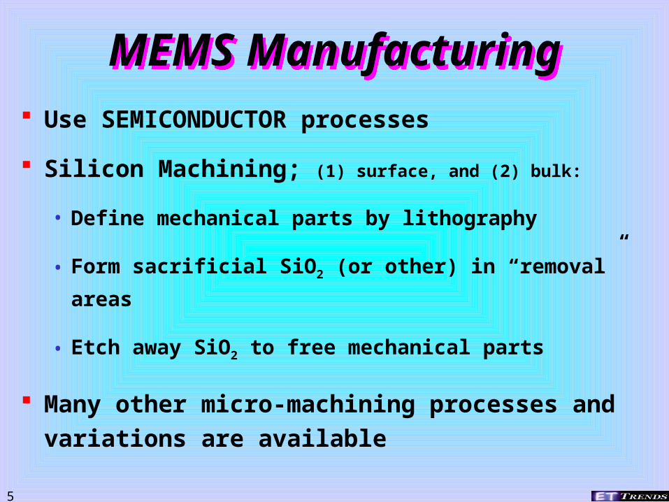
MEMS ManufacturingMEMS Manufacturing Use SEMICONDUCTOR processes
Silicon Machining; (1) surface, and (2) bulk:
• Define mechanical parts by lithography
• Form sacrificial SiO2 (or other) in “removal” areas
• Etch away SiO2 to free mechanical parts
Many other micro-machining processes and
variations are available
6
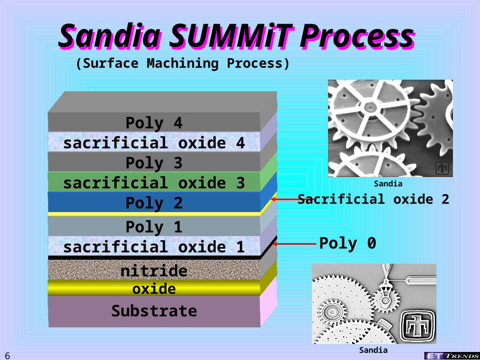
Sandia SUMMiT Process
Sandia SUMMiT Process
Substrate
oxidenitride
sacrificial oxide 1Poly 1
Poly 2sacrificial oxide 3
Poly 3sacrificial oxide 4
Poly 4
Poly 0
Sacrificial oxide 2Sandia
Sandia
(Surface Machining Process)

7
MEMS Bulk FabricationMEMS Bulk Fabrication
Start with single crystal silicon
Apply etch resist (mask)
Can selectively implant stop etch into Si
Etch unwanted silicon
• Wet/chemical (anisotropic; etches alone planes)
• Dry plasma (high resolution)
Simpler shapes, lowest cost (?)
8
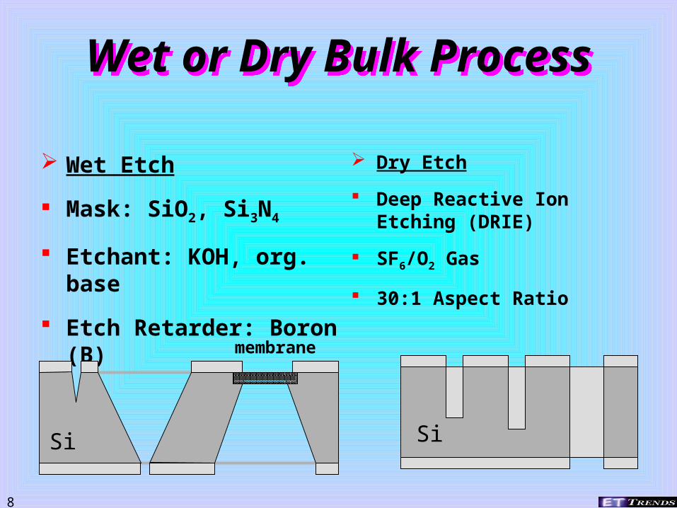
Wet or Dry Bulk Process
Wet or Dry Bulk Process
Wet Etch
Mask: SiO2, Si3N4
Etchant: KOH, org. base
Etch Retarder: Boron (B)
Dry Etch
Deep Reactive Ion Etching (DRIE)
SF6/O2 Gas
30:1 Aspect Ratio
SiSi
membrane
9
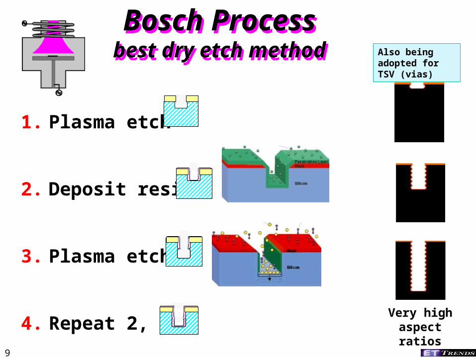
Bosch Processbest dry etch methodBosch Process
best dry etch method
1. Plasma etch
2. Deposit resist
3. Plasma etch
4. Repeat 2, 3.Very high
aspect ratios
Also being adopted for TSV (vias)

10
LIGA ProcessLIGA Process LIGA mask design
Mask fabrication
Substrate preparation
X-ray exposure
X-ray resist development
Electroplate
Panelization
Replication
Lithographie Galvanoformung Abformung

11
MEMS ReleaseMEMS Release
Remove sacrificial layer
Oxide 2
Si Etc
h &
Rel
ease
More fragile
Final stepbefore packaging
A critical very step
Remove holding structure• Wet Chem Etch; dissolve silica ; SiO2
• Dry Plasma Etch
Packaging foundry may run this process

12
Wafer BondingWafer Bonding Fabricate MEMS devices• Pumps, pressure sensors• Values, controllers• Chambers; analyzers, reactors
Integrated MEMS• Electronics; logic, memory, sensors• Optics, photonics
Pre-packaging; capping wafers
Complete Wafer-Level Package (WLP)

13
Wafer Bonding Methods
Wafer Bonding Methods
PROCESS Temp Hermeticity Reliability Availability Cost
Metallurgical mod-high
high excel. high mod.
Fusion high high excel. mod mod.
Anodic mod high excel. mod mod.
Inorg. adhes. mod good-high excel. high mod.
Brazing high high excel. high mod.Laser-assisted localized ~ ~ limited ~Polymer, thermoset
low Non-hermetic good high low
Polymer, thermoplastic
mod. Near-hermetic good limited low
Polymer, UV low Non-hermetic mod limited low
14
Summary of FabricationSummary of Fabrication
MEMS can use existing semiconductor mfg
Major boost with existing infrastructure
Parallel process; productivity
Older foundries 6” moving to 8” (don’t need 12”)
Combine CMOS logic & MEMS
MEMS can build almost any macrostructure
Cavities, electronics may require wafer bonding


