
1
Digital Circuit Implementation Issues PLAs, PALs, ROM’s, FPGA’s Packaging Issues Look Up Table method Multiplexer Method RAM & ROM method Xilinx and Actel Examples of FPGA’s I/O for FPGA’s Comparison of Various FPGAs
Lecture 12

2
Names associated with this field :
PLD… PAL, PLA, FPLA SPLD, CPLD
GA, MPGA, ASIC, Full Custom , Semi Custom,
ROM, PROM, EPROM, EEPROM
FPGA, LCA, VLSI, ULSI, GSI, MCM, SOC, NoC
NEW** FPOA**Field Programmable Object Array (FPOA) product from Mathstar.
They offer FPGA-like functionality but replaced the CLBs with ALU blocks instead. They also run at 1GHz and have large memory blocks.
Ideal associated characteristics
Field Programmability
Availability of CAD tools
CAD tool friendliness
Performance
Prototyping Costs, Production Time, Yield
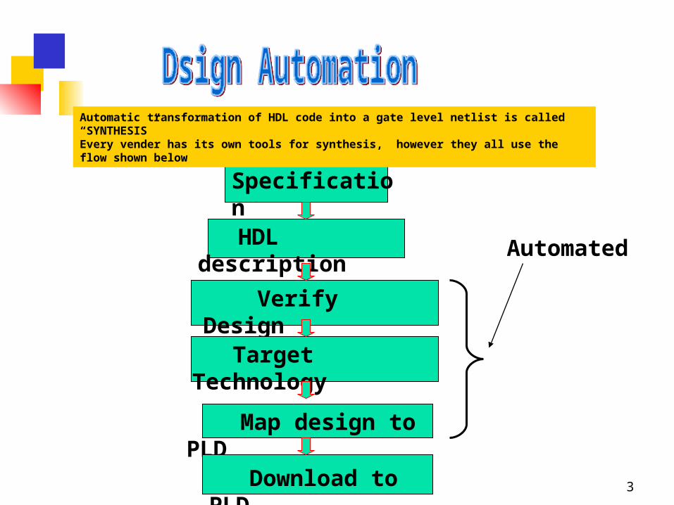
3
Specification
HDL description
Verify Design
Target Technology
Map design to PLD
Download to PLD
Automated
Automatic transformation of HDL code into a gate level netlist is called “SYNTHESIS”Every vender has its own tools for synthesis, however they all use the flow shown below

4
Any Sum of Product (SOP)can be represented by AND-OR.
ROM,PAL,PLA are different optimized implementation Of Given Circuit using the AND-OR planes.
ROM: AND Fixed, OR Programmable
PAL: AND Programmable, OR fixed
PLA: AND Programmable, OR Programmable
FPGA: Programmable Logic Blocks, Programmable Interconnect

5
Logic Gates and Programmableswitches
Inputs(logic variables)
Outputs(logic functions)
Programmable Logic Device as a black box

6
Input buffersAnd inverters
ANDPlane
ORPlane
x1 x2 xn-1 xn
x1 x1 xn xnP1
Pk
General Structure of PLD – Programmable Logic Device
Any combinational logic can be implemented with Sum of Productwhich is AND-OR implementation.
f1
fm

7
AND OR DEVICEFixed Fixed Not
Programmable
Fixed Programmable PROM
Programmable Fixed PAL
Programmable Programmable PLA

8
x1 x2 x3
P1
P2
P3
P4
f1 f2
Programmable Fuses Connections
OR plane
SUM
AND plane

9
OR plane
P1
AND plane
x1 x2
x3
P2
P3
P4
f1 f2

10
Advantages of PLA
Efficient in terms of area needed for implementation on an IC chip
Often included as part of larger chips such as microprocessors
Programmable AND and OR gates

11
OR plane (Fixed)
P1
AND plane (Programmable)
x1 x2 x3
P2
P3
P4
f1
f2

12
PAL - Programmable Array Logic
PLA have higher programmability than PAL, however they have lower speed than PAL Solution PAL for higher speed.
Programmable AND, Fixed OR
PAL - Simpler to manufacture, cheaper than PLA and have better performance

13
Flip-flops store the value produced by the OR gate output at a particular point and can hold it indefinitely.
Flip-flop output is controlled by the clock signal. On 0-1 transition of clock, flip-flop stores the value at its D input and latches the value at Q output.
2-to-1 multiplexer selects an output from the OR gate output or the flip-flop output. Tri-state buffers are placed between multiplexer and the PAL output.
Multiplexer’s output is fed back to the AND plane in PAL, which allows the multiplexer signal to be used internally in the PAL. This facilitates the implementation of circuits that have multiple stages (levels or logic gates).

14
D Q
Select Enable
f1
Clock
To AND plane
Flip-flop
For additional flexibility, extra circuitry is added at the output of each OR gate. This is also referred to macrocell.

15
Example: FSM Implementation
S2 = P’ Q y1, R2 = y2,
S1 = P’ Q’ , R1 = Q + P Z= y2 y1’ P Q’ ,
P & Q – are inputsy2 & y1 are the states
Z is the output

16
User circuits are implemented in the programmable devices by configuring or programming these devices. Due to the large number of programmable switches in commercial chips; it is not feasible to specify manually the desired programming state for each switch. CAD systems are used to solve this problem.
Computer system that runs the CAD tools is connected to a programming unit.After design of a circuit has been completed, CAD tool generates a file (programming file or fuse map) that specifies the state of each switch in PLD. PLD is then placed into the programming unit and the programming file is transferred from the computer system to the unit. Programming unit then programs each switch individually.
17
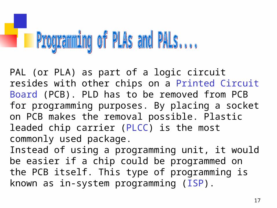
PAL (or PLA) as part of a logic circuit resides with other chips on a Printed Circuit Board (PCB). PLD has to be removed from PCB for programming purposes. By placing a socket on PCB makes the removal possible. Plastic leaded chip carrier (PLCC) is the most commonly used package.Instead of using a programming unit, it would be easier if a chip could be programmed on the PCB itself. This type of programming is known as in-system programming (ISP).

18
Simple PLDs,Single AND_OR planeIt is configured by programming the AND and OR plane, or may be the Flip Flop inclusion and feedback selection,Usually has less than 32 I/OThey are available in DIP (Dual in line package), PLCC (Plastic Lead Chip Carrier up to 100 pins. Usually less than 100 equivalent gates.
Complex PLDsMultiple AND-OR planesExtend the concept of the simple PLDs further by incorporating architectures that contain several multiple logic block PAL models. Most CPLD use programmable interconnect. Can accommodate from 1000 to 10,000 equivalent gates.Are available in PLCC and QFP (Quad Flap Pack) up to 200 pins

19
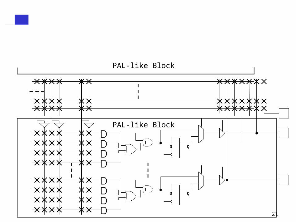
Chips containing PLDs are limited to modest sizes, typically supporting number of input and output more than 32. To accommodate circuits that require more input and outputs, either multiple PLAs or PALs can be used or a more sophisticated type of chip, called a complex programmable logic device (CLPD).CLPD is made up of multiple circuit blocks on a single chip, with internal wiring to connect the circuit blocks.
The structure of CLPD is shown on the next slide. It includes four PAL-like blocks connected by interconnection wires. Each block in turn is connected to a sub-circuit I/O block, which is attached to a number of input and output pins.

20
PAL-like block
PAL-like block
PAL-like block
PAL-like block
Interconnection Wires
I/Ob
lock
I/Ob
lock
I/O
blo
ckI/O
blo
ck
21
D Q
D Q
PAL-like Block
PAL-like Block

22
CLPD uses quad flat pack (QFP) type of package. QFP package has pins on all four sides and the pins extend outward from the package with a downward-curving shape. Moreover, QFP pins are much thinner and hence, they support a larger number of pins when compared to the PLCC packing.
Most CPLDs contain the same type of switch as in PLDs. Here, a separate programming unit is not used due to two main reasons. Firstly, CLPDs contain 200 + pins on the package, and these pins are often fragile and easily bent. Secondly, a socket would be required to hold the chip. Sockets are usually quite expensive and hence, add to the overall cost incurred.

23
CLPD usually support the ISP technique. A small connector is included on the PCB and is connected to a computer system. CLPD is programmed by transferring the programming information from the CAD tool to into the CLPD.
The circuitry on the CLPD that allows this type of programming is called JTAG, Joint Test Action Group port, and is standardized by the IEEE.
JTAG is a non-volatile type of programming i.e programmed state is retained permanently (for example, in case of power failure, CLPD retains the program).

24
The distinction between the two is blurred
Although PLDs started as small devices, today’s PLDs are anything but simple.
FPGAs fill the gap between PLDs and complex ASICs
In both cases, you can program the devices yourself, using design entry and simulation.
All FPGAs have regular array of basic cells that are configured by the programmer
using special software that program the chips by programming the interconnection.
Each vendor has tool supplier that provides custom tools for their products.
The programming methodology is usually non permanent, allowing re-programmability

25
Advantage:
FPGAs have lower prototyping costs
FPGAs have shorter production times
Disadvantage:
FPGAs Have lower speed of operation in comparison to MPGAs
Say by a factor 3 to 5
FPGAs have a lower logic density in comparison to MPGAs
Say by a factor of 8 to 12

26
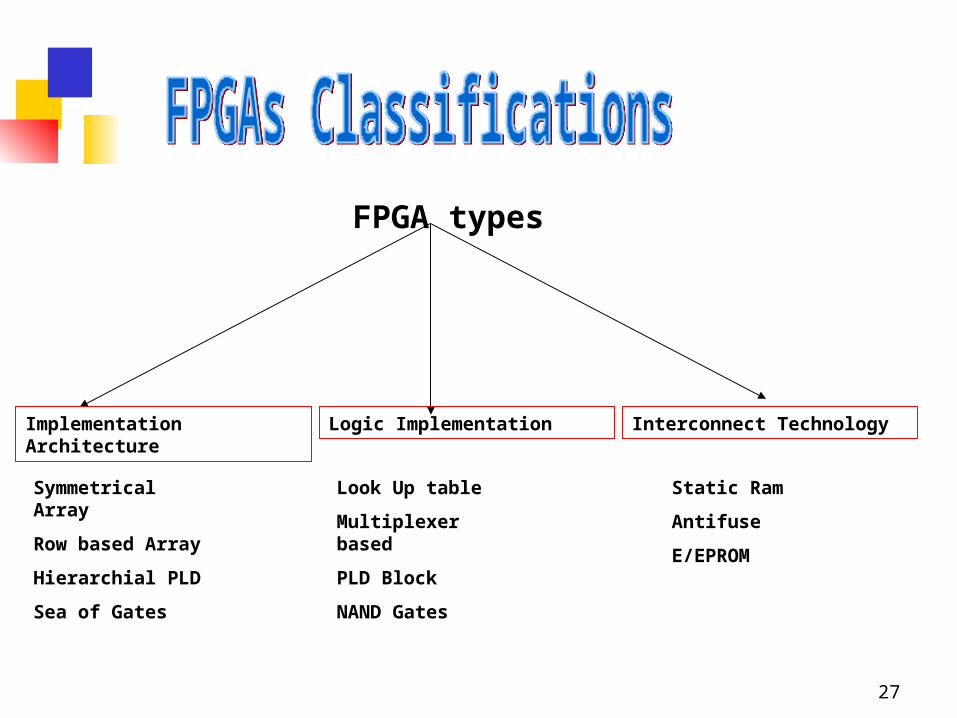
Consists of uncommitted logic arrays and user programmable interconnection.
The interconnect programming is done through programmable switches
The Logic circuits are implemented by partitioning the logic into blocks and then interconnecting the blocks with the programmable switches
The architecture of an FPGA varies from device to device , vendor to vendor it can be based on CPLDs, EPROMS, EEPROMS, LUT, Buses, PALS
The interconnect is also varied from EPROM, static RAM, antifuse, EEprom
27
Implementation Architecture
Logic Implementation Interconnect Technology
Symmetrical Array
Row based Array
Hierarchial PLD
Sea of Gates
Look Up table
Multiplexer based
PLD Block
NAND Gates
Static Ram
Antifuse
E/EPROM
FPGA types
28
Consists of an array of uncommitted elements that can be interconnected in a general way. Like
a PAL the interconnection between the elements are user programmable.
The interconnect compromises segments of wires, where segments may be of various lengths.
Present in the interconnect are programmable switches that serve to connect the logic blocks to
the wire segments or one wire segment to another. Logic circuits are implemented in the FPGA
by partitioning the logic into logic blocks and then interconnecting the blocks as required via
switches. To facilitate the implementation of a wide variety of circuits, it is important that an
FPGA be as versatile as possible. There are many ways to design an FPGA, involving trade offs
in the complexity and flexibility of both the logic blocks and the interconnection resources.
29
Logic Block and Interconnection:
The architecture of logic blocks vary from simple combinational logic to complex EPROMs,
LUT, Buses etc.. The routing architecture can also be variable including pass-transistors
controlled by static RAM cells, anti fuses, EPROM transistors. Each company provides
a
variety of architecture of the logic blocks and routing architecture.

30
Interconnect Resources
Logic Block I/O Cell
CONCEPTUAL FPGA

31
Row-basedInterconnect
Logic Block
PLD BlockInterconnectoverlayed on LogicBlocks
Logic Block
Interconnect
Sea-of-GatesHierarchical PLD
Interconnect
Symmetrical Array
Classes of common commercial FPGA
Various Block Architecture & Routing Architecture

32
Altera 40nm FPGA’ahttp://www.altera.com/literature/br/br-stratix-iv-hardcopy-iv.pdf
Table 2. HardCopy IV E Devices Overview
Device (1) ASICGates
(2)
MemoryBits(3)
I/O Pins PLLs FPGAPrototype
HC4E2YZ 3.9M 8.1 296 - 480 4 EP4SE110
HC4E3YZ 9.2M 10.7 296 - 480 4 EP4SE230
HC4E4YZ 7.6M 12.1 - 13.3 392 - 864 4/8/12 EP4SE290
HC4E5YZ 9.5M 16.8 480 - 864 4/8/12 EP4SE360
HC4E6YZ 11.5M 16.8 736 - 880 8/12 EP4SE530
HC4E7YZ 13.3M 16.8 736 - 880 8/12 EP4SE680
Notes:1.Y = I/O count, Z = package type (see the product catalog for more information) 2.ASIC gates calculated as 12 gates per logic element (LE), 5,000 gates per 18 x 18 multiplier(SRAMs, PLLs, test circuitry, I/O registers not included in gate count) 3.Not including MLABs
33
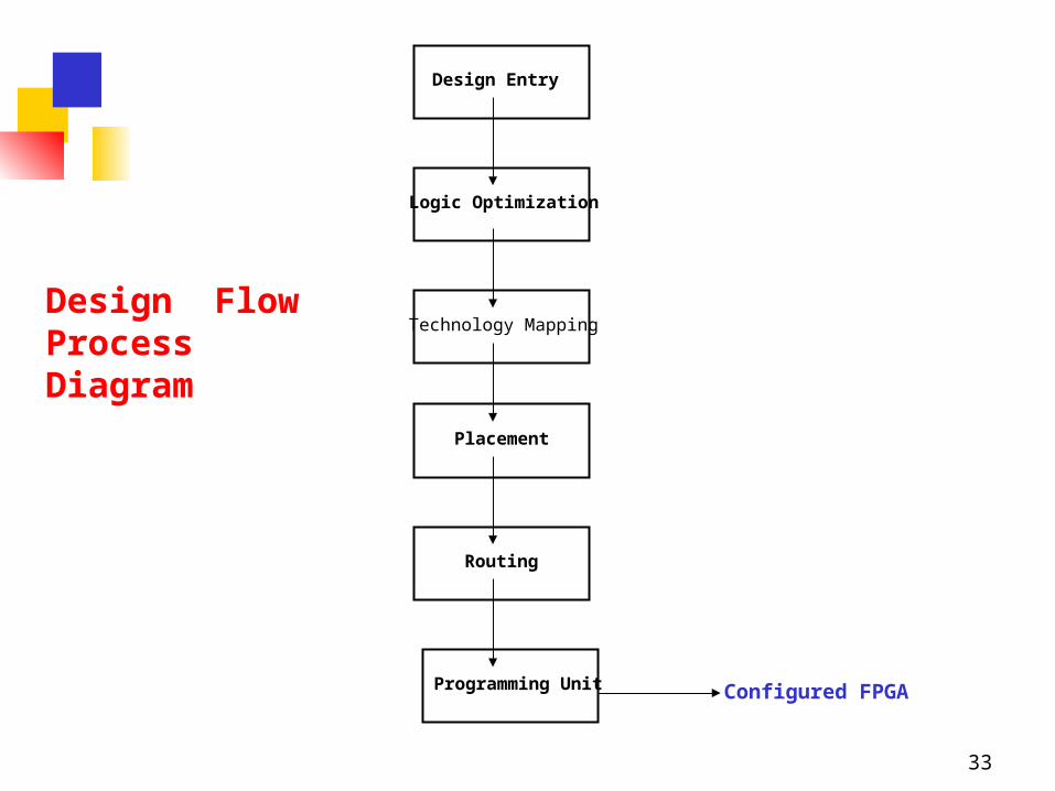
Design Entry
Logic Optimization
Technology Mapping
Placement
Routing
Programming Unit Configured FPGA
Design FlowProcess Diagram

35
A designer implementing a circuit on an FPGA must have access to CAD
tools for that type of FPGA. The following steps summarize the process
1) Logic Entry: Either simulate capture or entering VHDL description or
specifying Boolean expansions.
2) Translate to Boolean & optimize
3) Transform into a circuit of FPGA logic blocks through a technology mapping
program (minimizing # of blocks).
4) Decides what to place in each block in FPGA array (minimizing total
length of interconnect)
5) Assigns the FPGA’s wire segments and chooses programmable switches to
establish required interconnection.

36
6) The output of the CAD system is fed to the programming unit that
configures the final FPGA chip.
Depending upon correct VHDL or design entry, the entire process of
implementing a circuit in an FPGA can take from a few minutes to
about and hour.

37
Any logic function can expanded in form of a Boolean variable:
F= A.F + A.F
For example assume F= A.B + A.B.C + A . B. C
Then in the expansion
F = A [A.B + A.B.C + A. B. C]+ A [ A.B + A.B.C + A. B. C ]
= A. [B.C ] + A [ B + C ] Then this can be implemented with a
MUX
F
A
F1
F2
F1 F2

38
F1 = B . C F2 = B + C
These functions can be broken down further into:
F1 = B ( B . C ) + B ( B . C )
= B . C + B . 0
F10
CB
F2 = B ( B + C ) + B ( B + C )
= B . 1 + B . C
F2C
1B
F2C
1B
F10
CB
F
A
Overall Function
01
MUX
Control

39
Functions can also be expanded into canonical form. Then F is expanded as
F= A.B + A.B.C + A . B. C
F = A . B ( C + C ) + A . B . C + A . B . C
= A . B . C + A . B . C + A . B . C + A . B . C
= A . B . C + A ( B . C + B . C + B . C )
= A . F1 +A. F2 In turn this can be implemented in MUX:
F
A
F1
F2

40
Therefore 2-1 multiplexer is a general block that can represent any gate:
AND Gate
F = A . BF = A . ( A . B ) + A ( A . B )
= A . B + A . 0
F0
BA
F = A ( A + B ) + A’ ( A + B ) = A + AB + A’. B = A . 1 + A’ . B
F1
A
B
F = A . B + A . B
CB
A
B
OR Gate Ex-OR

41
10 ‘1’
‘1’
Functions that can be implemented using just 2:1 MUX (No inverter at the input).
If there are no 2 input rails available, XOR, NAND & NOR cannot be implementeddirectly. There is a need for more MUXs to be used as inverters.

42
ACT1 module has three 2:1 Muxs with AND-OR logic at the select of final
MUX and implements all 2 input functions, most 3 input and many 4 input
functions.
Software module generator for ACT1 takes care of all this.
Apart from variety of combinational logic functions, the ACT1 module can
implement sequential logic cells in a flexible and efficient manner. For
example an ACT1 module can be used for a transparent Latch or two
modules for a flip flop.
43
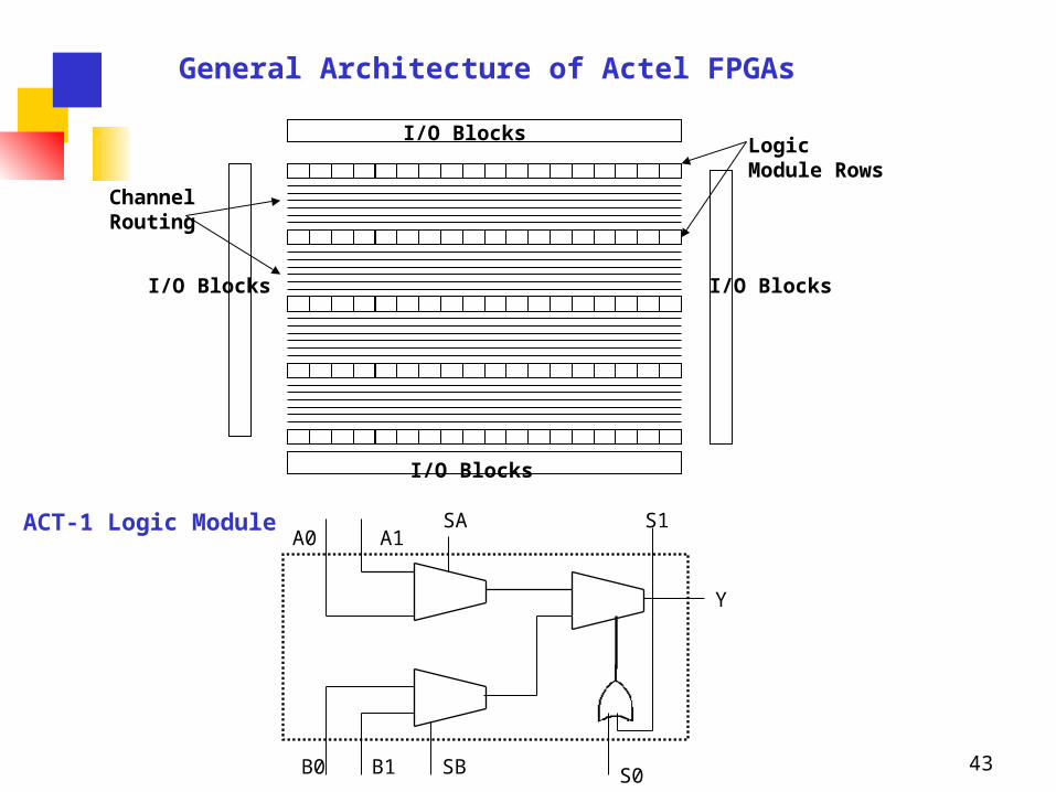
I/O Blocks
I/O Blocks
LogicModule Rows
I/O BlocksI/O Blocks
Channel Routing
General Architecture of Actel FPGAs
SAA0 A1
B0 B1 SB
S1
Y
S0
ACT-1 Logic Module
44
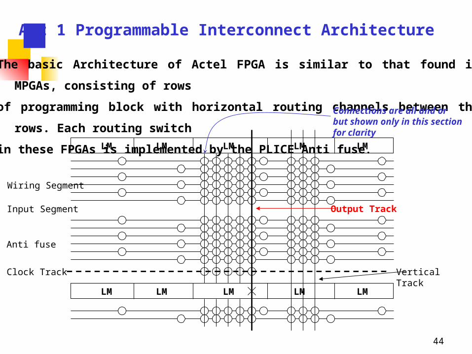
LMLMLMLMLM
LMLMLMLMLM
Input Segment
Wiring Segment
Anti fuse
Clock Track VerticalTrack
Output Track
The basic Architecture of Actel FPGA is similar to that found in MPGAs, consisting of rows
of programming block with horizontal routing channels between the rows. Each routing switch
in these FPGAs is implemented by the PLICE Anti fuse. Connections are all and orbut shown only in this sectionfor clarity
Act 1 Programmable Interconnect Architecture

45
M1A0
A1
SA
B0B1
SB
S0S1
O1
S3F2
S
F1
M2
F01
01
01
A0
SA
B0
B1
S3F2
F1
M2
S0S1
SB
A1
O1
S3
F
M1D
‘1’
C
D‘1’
A
‘0’B
O1
S3F2
S
F1
M2
F01
01
01 F = A.B + B.C +D
= B [A.B + B.C + D] + B[A.B + B.C + D] = A.B + B.D + B.C + B.D = B.(A+D) + B (C+D)
ACTEL Logic Module ACTEL – Implementation using pass transistors
ACTELAn example logic macro

46
M1D00D01
B1
OUTYD10D11
A1
B0A0
S1S0
ACTEL ACT C-ModuleM1
D00D01
B1
D10D11
A1
CLRA0
S1S0
QSE
CLK
Y
CLK
D00D01
B1
D10D11
A1
B0A0
S1S0
QSE
Y
CLR
S-Module (ACT 2)
S-Module (ACT 3)
10
1 0
Z Z QD
C2
C1CLR
Combinational Logic for Clear and Clock
Master Latch
SlaveLatch
SE (Sequential Element)
D QCLK C2
C1CLR
CLR
SE

47
ACT1 module is simple logical block. It does not have built in function to
generate a Flip Flop. Although it can generate a FF if required.
ACT2 and ACT3 that has separate FF module is used for Sequential
Circuits.
Timing Models & Critical Path
Exact timing (delays) on any FPGA chip cannot be estimated until
place and routing step has been performed. This is due to the delay
of the interconnect. A critical path of SE in is shown on the next
slide.
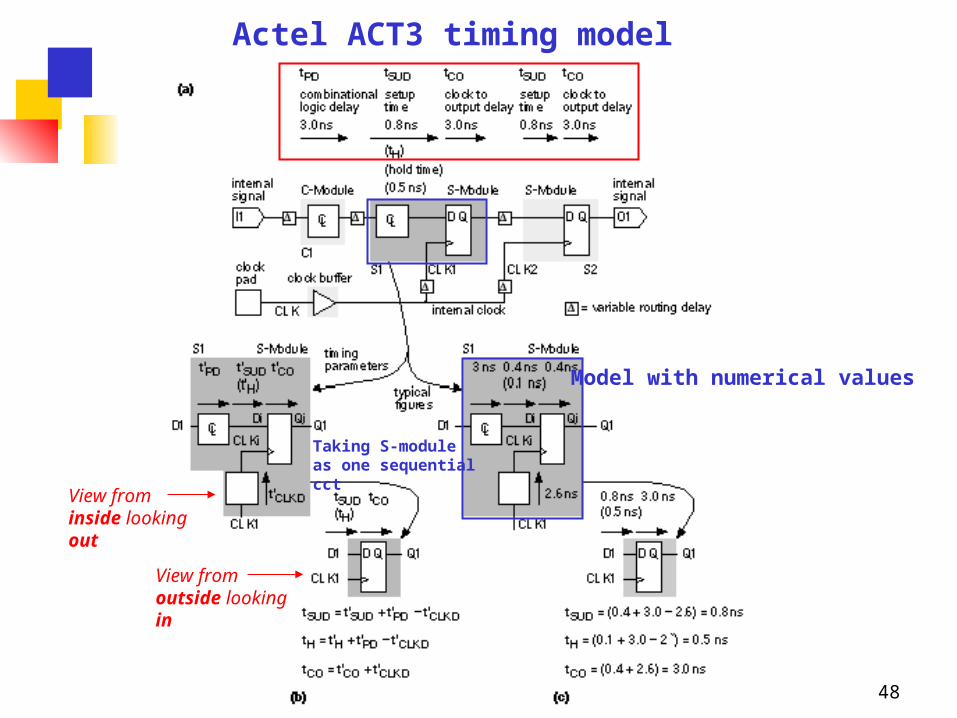
48
View frominside lookingout
View fromoutside lookingin
Model with numerical values
Taking S-moduleas one sequential cct
Actel ACT3 timing model

49
TABLE 5.2 ACT 3 timing parameters* [1]
Fanout
Family Delay* 1 2 3 4 8
ACT 3-3 (data book) t PD 2.9 3.2 3.4 3.7 4.8
ACT3-2 (calculated) t PD /0.85 3.41 3.76 4.00 4.35 5.65
ACT3-1 (calculated) t PD /0.75 3.87 4.27 4.53 4.93 6.40
ACT3-Std (calculated) t PD /0.65 4.46 4.92 5.23 5.69 7.38
* V DD = 4.75 V, T J ( junction) = 70 °C. Logic module + routing delay. All propagation delays in
nanoseconds.* The Actel '1' speed grade is 15 % faster than 'Std'; '2' is 25 % faster than 'Std'; '3' is 35 % faster than 'Std'.

50
TABLE 5.3 ACT 3 Derating factors* [1]
Temperature T J ( junction) / °C
V DD / V –55 –40 0 25 70 85 125
4.5 0.72 0.76 0.85 0.90 1.04 1.07 1.17
4.75 0.70 0.73 0.82 0.87 1.00 1.03 1.12
5.00 0.68 0.71 0.79 0.84 0.97 1.00 1.09
5.25 0.66 0.69 0.77 0.82 0.94 0.97 1.06
5.5 0.63 0.66 0.74 0.79 0.90 0.93 1.01
•Worst-case (Commercial): V DD = 4.75 V, T A (ambient) = +70 °C. Commercial: V DD = 5 V ± 5 %, •T A (ambient) = 0 to +70 °C. Industrial: V DD = 5 V ± 10 %, T A (ambient) = –40 to +85 °C.
•Military V DD = 5 V ± 10 %, T C (case) = –55 to +125 °C.

51
A k input LUT can implement any Boolean function of k variables. The
inputs are used as addresses that can retrieve the 2k by 1-bit memory that
stores the truth table of the Boolean function.
Since the size of the memory increases with the number of inputs, k, in
order to optimize this mapping and reduce the size of the memory there are
a variety of algorithms that map a Boolean network, from a given
equation, into a circuit of k-input LUT. These algorithms minimize either
the total number of LUTs or the number of levels of LUTs in the final
circuit. Minimizing the total number of LUTs reduces the CLB
requirements while minimizing the levels of LUTs improves the delay.
Look Up Table (LUT)

52
f1= (abc + def) (g + h + i) (jk +lm)
a b c d e f g h l j k l m
x y
z
a b c j k l m
x y
z
g h i
d e f
4 input LUT
5 input LUT
This can be implemented by Four 5 input LUT

53
Two input LUTBefore programming
0/1
0/1
0/1
0/1
x1 x2 f1
0 0 1
0 1 0
1 0 0
1 1 1f1= x1 x2 + x1 x2
Function to be implemented
Storage Cell contents in the LUTAfter programming
1
0
0
1

54
Storage Cell contents in the LUTAfter programming
1
0
0
1
0
1
0
1
f1
f1= x2 x1+ x2 x1
55
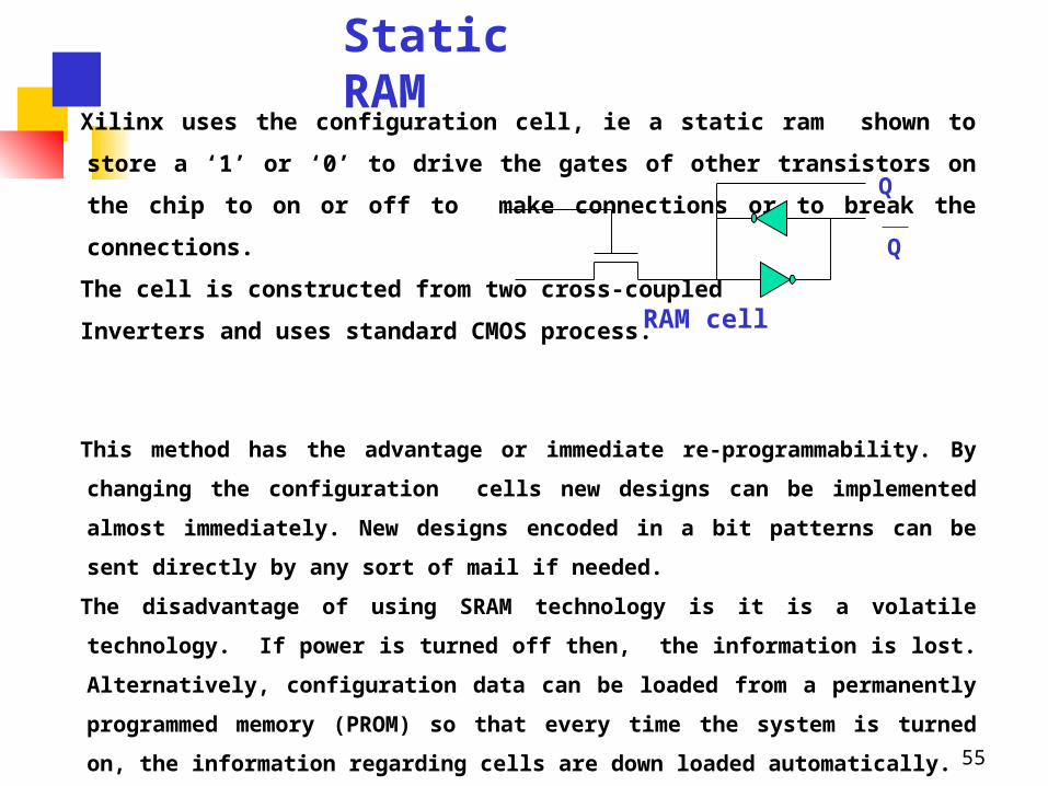
Xilinx uses the configuration cell, ie a static ram shown to store a ‘1’ or ‘0’ to drive the
gates of other transistors on the chip to on or off to make connections or to break the
connections.
The cell is constructed from two cross-coupled
Inverters and uses standard CMOS process.
This method has the advantage or immediate re-programmability. By changing the
configuration cells new designs can be implemented almost immediately. New designs encoded
in a bit patterns can be sent directly by any sort of mail if needed.
The disadvantage of using SRAM technology is it is a volatile technology. If power is turned off
then, the information is lost. Alternatively, configuration data can be loaded from a
permanently programmed memory (PROM) so that every time the system is turned on, the
information regarding cells are down loaded automatically.
The S ram based FPGAs have a larger area overhead than the fused or anti fused devices
Static RAM
RAM cell
Q
Q

56
RAM cell
Routingwire
RAM cell
Routingwire
Routing wire
RAM cell
RAM cell
MUX
To logic cell input

57
An anti fuse is normally an open circuit until a programming current is forced though it (about
5mA).
The two prominent methods are Poly to Diffusion (Actel) and Metal to Metal (Via Link). In a
Poly-diffusion anti fuse the high current density causes a large power dissipation in a small
area.
Anti fuse Polysilicon
n+ Diffusion
Dielectric
2 λ
Anti fuse Polysilicon
Anti fusePolysilicon
Anti fuse
n+ anti fuse diffusion
Contact
The actual anti fuse link is less than 10nm x 10nm
Anti fuse (Actel)

58
This will melt a thin insulating dielectric between polysilicon and diffusion and form a thin
(about 20nm in diameter) permanent, and resistive silicon link. The programming process also
drives dopand atoms from the poly and diffusion electrodes. The fabrication process and
Programming current controls the average resistance of blown anti fuses.
Actel Device # of Anti fuses
A1010 112,000
A1225 250,000
A1280 750,000 250 500 750 1000
Anti fuse Resistance in Ω
% Blown Anti fuses
To design and program an Actel FPGA, designers iterate between design entry and simulation
when design is verified both by functional and timing tests. Chip is plugged into a socket on a
special programming box that generates the programming voltage.
Anti fuse (Actel)….
59
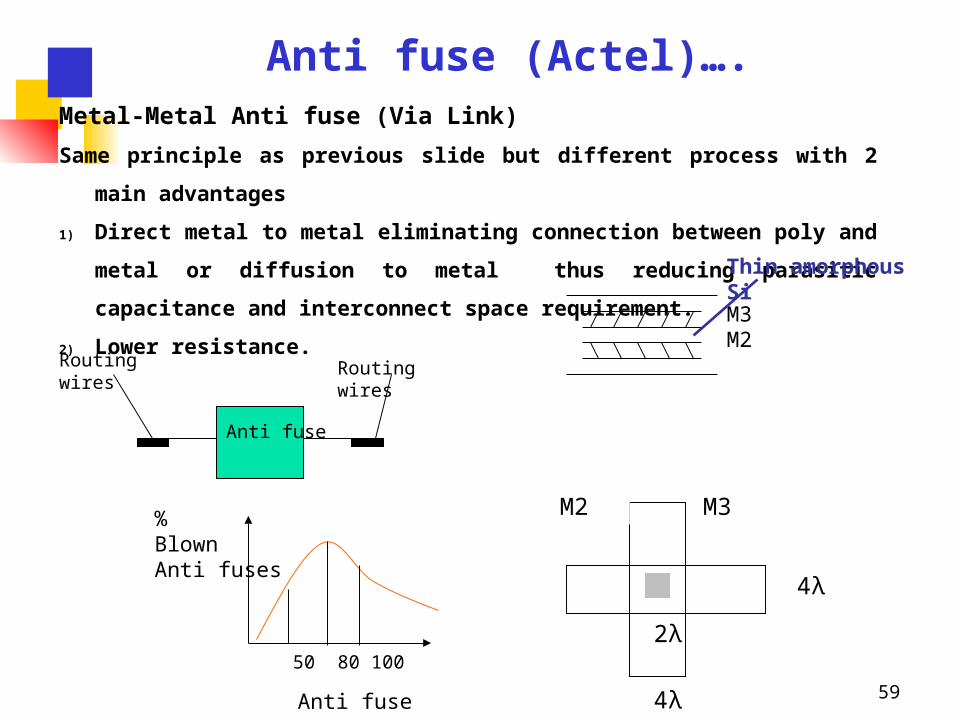
Metal-Metal Anti fuse (Via Link)
Same principle as previous slide but different process with 2 main advantages
1) Direct metal to metal eliminating connection between poly and metal or diffusion to
metal thus reducing parasitic capacitance and interconnect space requirement.
2) Lower resistance.
Anti fuse
Routing wires
Routing wires
M3M2
Thin amorphous Si
M3
4λ
M2
4λ
2λ 50 80 100
Anti fuse Resistance Ω
% Blown Anti fuses
Anti fuse (Actel)….

60
Altera MAX 5K and Xilinx ELPDs both use UV-erasable “electrically programmable
read-only ` memory” (EPROM) cells as their programming technology. The EPROM cell
is almost as small as an anti fuse.
GroundS D
G2
G1
S D
G2
G1+Vgs>Vtn
+Vpp
+Vgs>Vtn
Vds
No channel
G2
G1
UV light
EPROM and EEPROM

61
Altera MAX 5K and Xilinx ELPDs both use UV-erasable “electrically programmable
read-only memory” (EPROM) cells as their programming technology. The EPROM
cell is almost as small as an anti fuse.
An EPROM looks like a normal transistor except it has a second floating gate.
(a) Applying a programming voltage Vpp (>12) to the drain of the n-channel, programs
the cell. A high electric field causes electrons flowing towards the drain to move so fast
they “jump” across the insulating gate oxide where they are trapped on the bottom of
the floating gate.
(b) Electrons trapped on the floating gate raise the threshold voltage. Once programmed
an n-channel EPROM remains off even with Vdd applied to the gate. An
unprogrammed n-channel device will turn on as normal with a top-gate voltage Vdd.
(c) Exposure to an ultra-violet (UV) light will erase the EPROM cell. An absorbed light
quantum gives an electron enough energy to jump for the floating gate.
EPROM and EEPROM….

62
EPLD package can be bought in a windowed package for development, erase it and use it
again. Programming EEPROM transistors is similar to programming an UV-erasable EPROM
transistor, but the erase mechanism is different. In an EEPROM transistor and electric field is
also used to remove electrons from the floating gate of a programmed transistor. This is faster
than the UV-procedure and the chip doesn’t have to removed from the system.
EPROM and EEPROM….
63
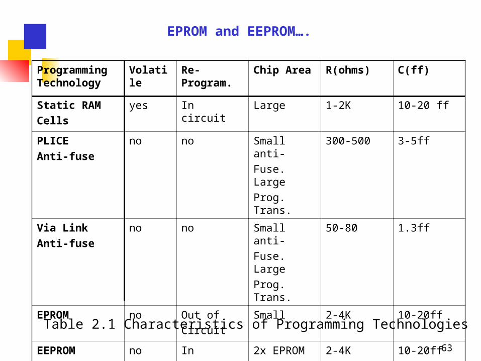
Programming Technology
Volatile
Re-Program.
Chip Area R(ohms) C(ff)
Static RAMCells
yes In circuit Large 1-2K 10-20 ff
PLICEAnti-fuse
no no Small anti-Fuse. LargeProg. Trans.
300-500 3-5ff
Via LinkAnti-fuse
no no Small anti-Fuse. LargeProg. Trans.
50-80 1.3ff
EPROM no Out ofCircuit
Small 2-4K 10-20ff
EEPROM no In Circuit
2x EPROM 2-4K 10-20ff
EPROM and EEPROM….
Table 2.1 Characteristics of Programming Technologies

64 Creating a wired-AND with EPROM cells [3]
Structure of a FAMOS transistor [3]
F= A + B + C + D + ……. = A . B . C . D . ……..
First Level Polysilicon
Second Level Polysilicon
Field OxideGate Oxide

65
- Can be static RAM cells, Anti fuse, EPROM transistor and EEPROM transistors.
- The programming elements are used to implement the programmable connections
among the FPGA’s logic blocks, and a typical FPGA may contain some 5000,000
programming elements.
• The programming element should consume as little chip area as possible.
• The programming element should have a low “ON” resistance and very high “OFF”
resistance.
• The programming element contributes low parasitic capacitance to the wiring.
• It should be possible to reliably fabricate a large number of programming elements
on a singe chip
• Re-programmability is derived features for these elements.

66
FPGAs
Implementation Architecture:
-Symmetrical Array-Row based-Hierarchical PLD-Sea of Gates
Logic Implementation
-Look Up Table-Multiplexer based-PLD Block-NAND gates
Technology of Interconnection
- Static RAM- Anti fuse- EPROM- EEPROM
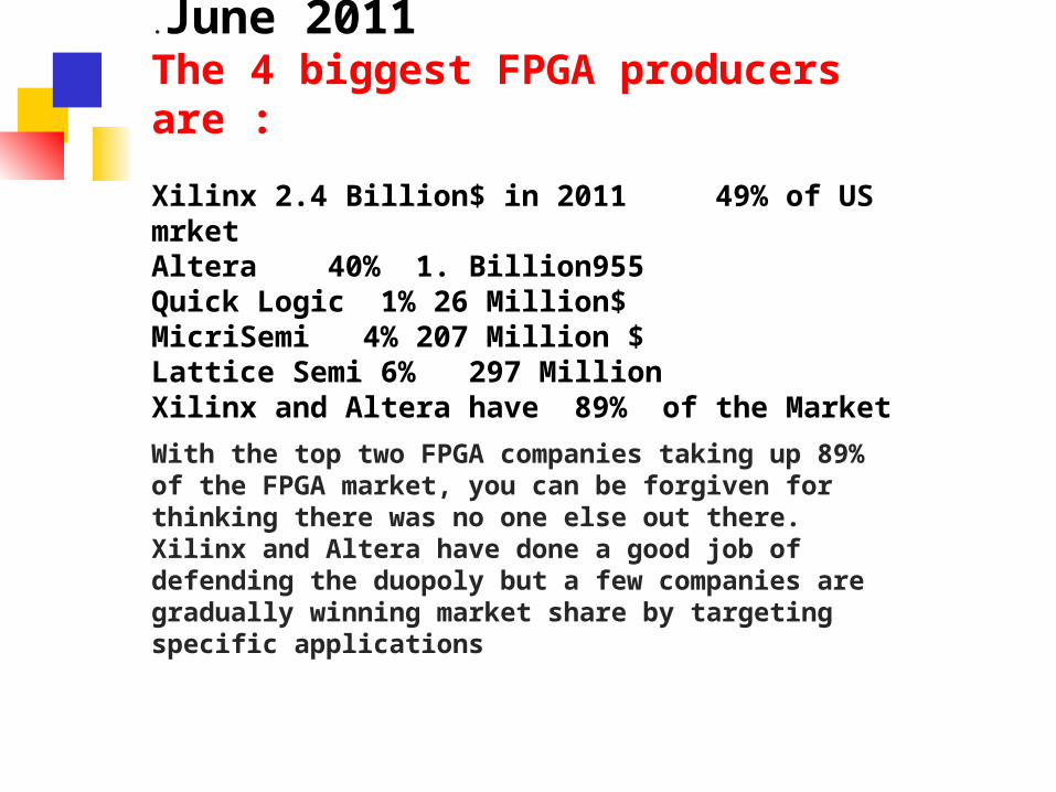
.June 2011The 4 biggest FPGA producers are :
Xilinx 2.4 Billion$ in 2011 49% of US mrketAltera 40% 1. Billion955 Quick Logic 1% 26 Million$MicriSemi 4% 207 Million $ Lattice Semi 6% 297 MillionXilinx and Altera have 89% of the Market
With the top two FPGA companies taking up 89% of the FPGA market, you can be forgiven for thinking there was no one else out there. Xilinx and Altera have done a good job of defending the duopoly but a few companies are gradually winning market share by targeting specific applications

Features Artix-7 Kintex-7 Virtex-7 Spartan-6 Virtex-6
Logic Cells 352,000 480,000 2,000,000 150,000 760,000
BlockRAM 19Mb 34Mb 68Mb 4.8Mb 38Mb
DSP Slices 1,040 1,920 3,600 180 2,016
DSP Performance (symmetric FIR)
1,248GMACS 2,845GMACS 5,335GMACS 140GMACS2,419GMACS
Transceiver Count 16 32 96 8 72
Transceiver Speed 6.6Gb/s 12.5Gb/s 28.05Gb/s 3.2Gb/s 11.18Gb/s
Total Transceiver Bandwidth (full duplex)
211Gb/s 800Gb/s 2,784Gb/s 50Gb/s 536Gb/s
Memory Interface (DDR3)
1,066Mb/s 1,866Mb/s 1,866Mb/s 800Mb/s 1,066Mb/s
PCI Express® Interface
Gen2x4 Gen2x8 Gen3x8 Gen1x1 Gen2x8
Agile Mixed Signal (AMS)/XADC
Yes Yes Yes Yes
Configuration AES Yes Yes Yes Yes Yes
I/O Pins 600 500 1,200 576 1,200
I/O Voltage1.2V, 1.35V, 1.5V, 1.8V, 2.5V, 3.3V
1.2V, 1.35V, 1.5V, 1.8V, 2.5V, 3.3V
1.2V, 1.35V, 1.5V, 1.8V, 2.5V, 3.3V
1.2V, 1.5V, 1.8V, 2.5V, 3.3V
1.2V, 1.5V, 1.8V, 2.5V
EasyPath Cost Reduction Solution
- Yes Yes - Yes
FPGA Comparison Table
69
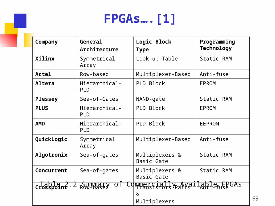
Company General Architecture
Logic BlockType
Programming Technology
Xilinx Symmetrical Array Look-up Table Static RAM
Actel Row-based Multiplexer-Based Anti-fuse
Altera Hierarchical-PLD PLD Block EPROM
Plessey Sea-of-Gates NAND-gate Static RAM
PLUS Hierarchical-PLD PLD Block EPROM
AMD Hierarchical-PLD PLD Block EEPROM
QuickLogic Symmetrical Array Multiplexer-Based Anti-fuse
Algotronix Sea-of-gates Multiplexers & Basic Gate
Static RAM
Concurrent Sea-of-gates Multiplexers & Basic Gate
Static RAM
Crosspoint Row-based Transistors Pairs &Multiplexers
Anti-fuse
FPGAs….[1]
Table 2.2 Summary of Commercially Available FPGAs

70
TAB (Taped Automated
Bonding)
PQFP(Plastic Quad Flat
Package)
PLCC(Plastic Leaded Chip
Carrier)
DIP(Dual In-line
Package)

TjJunction temperature operating range for commercial temperature 0 – 85 °CJunction temperature operating range for extended temperature 0 – 100 °CJunction temperature operating range for Industrial temperature –40 – 100 °CJunction temperature operating range for military temperature –55 – 125 °C
Prices---Xilinxhttp://www.digikey.ca website.Part number XC7A35T XC7A50T XC7A75T XC7A100TPrice(CAD) 68.13 102.30 120 166.66
Prices---AlteraFamily CycloneVEDevice 5CEBA2 5CEBA4 5CEBA5 5CEBA7Price 44.55 62.88 103.87 188.02
Power----Xilinx
Part number XC7A35T XC7A50T XC7A75T XC7A100TTotal On--‐Chip Power (W) 0.068 0.068 0.084 0.084

72
Classic Package Hierarchy [Intel Corp.]
BoardSilicon Die
~ .040”
~ .012“
Package

73
Area Array Packages
Cross Section of Flip-Chip Ball Grid Array(FC-BGA)

74
Which Package should we select?
Industry trend is going for Area Array Packages Bond wires contribute parasitic inductance According some policies industry is urged to
use pb-Free products The number of needed pins growing up Packaging Innovations
System In Package (SiP) Wafer Level Package (WLP)
Wafer Level Packaging (WLP)System in Package (SiP)

75
Todays generation of FPGAs consist of various mixes of configurable embedded Ips (large blocks) such as: SRAM, transceivers, I/Os, logic blocks, Arithematic units such as adders and multipliers and routing. Most FPGAs contains programmable logic components called logic elements (LEs) and a hierarchy of reconfigurable interconnects You can configure LEs to perform complex combinational functions, or merely simple logic gates. Most FPGAs, include memory elements, which may be simple flipflops or complete blocks of memory.
Today’s FPGAs structure
76
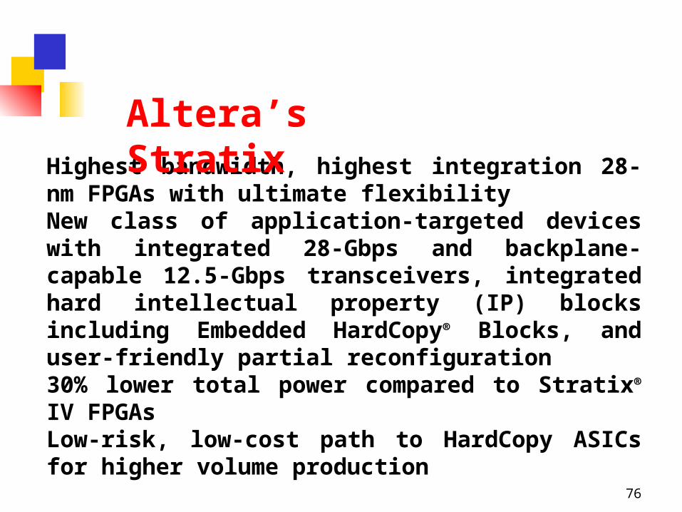
Highest bandwidth, highest integration 28-nm FPGAs with ultimate flexibilityNew class of application-targeted devices with integrated 28-Gbps and backplane-capable 12.5-Gbps transceivers, integrated hard intellectual property (IP) blocks including Embedded HardCopy® Blocks, and user-friendly partial reconfiguration30% lower total power compared to Stratix® IV FPGAsLow-risk, low-cost path to HardCopy ASICs for higher volume production
Altera’s Stratix

77
28-nm FPGAs providing industry’s lowest system cost and powerSix variants offer mix of logic, 3.125-Gbps or 5-Gbps transceivers, and single- or dual-core ARM Cortex-A9 hard processor systemDelivers up to 40 percent lower total power and up to 30 percent lower static power vs. the previous generationHigh level of integration with abundant hard IP blocks
Altera’s Cyclone

http://electronics.stackexchange.com/questions/128120/reason-of-multiple-gnd-and-vcc-on-an-ic

Current has to be distributed, it is impractical that any pad can take the total current. The resistance drop is prohibiting
Power coming in from any one pin will probably have to snake it's away around a lot of stuff to get to every part of the device. Multiple power lines gives the device multiple avenues to pull power from, which keeps the voltage from dipping as much during high current events.
Need for a clean supply voltage at certain areas.
Analog devices require special attention and probably different voltage supply.Heat distrubution, and removal
Reasons for having multiple supply lines.

http://electronics.stackexchange.com/questions/128120/reason-of-multiple-gnd-and-vcc-on-an-ic
The figure represents all of the power and ground pins on a Virtex 4 FPGA in a BGA package with 1513 pins. The FPGA can draw up to 30 or 40 amps at 1.2 voltsEvery I/O pin is adjacent to at least one power or ground pin, minimizing the inductance and therefore the generated crosstalk.

Altera’s Cyclone II FPGA Starter Development Board (around $200.)
81

82
References
[1] Michael J. S. Smith, “Application-Specific Integrated Circuits,”
Addison Wesley ISBN 0-201-50022-1[2] Xilinx Handbook[3] ACTEL Handbook[4] Rose J. et al. “ A classification and survey of
field programmable gate array architectures,” Proceedings of The IEEE, vol. 81,no. 7 1993
[5] Brown. S. et al, Field Programmable Gate Arrays.
Kluwer Academic 1992 ISBN 0-7923-9248-5

Xilinx Trainig courses
83
http://www.xilinx.com/training/xilinx-training-courses.pdf
Xilinx PCI-Express , 2- day training course
http://www.xilinx.com/training/connectivity/designing-a-logicore-pci-express-system.htm

84
General Architecture of Xilinx FPGAs
I/O Block
Vertical Routing Channel
ConfigurableLogic Block
HorizontalRouting Channel

85
Basic logic cells CLBs(Configurable Logic Blocks) are bigger and more complex than the
Actel or Quick Logic cells. The Xilinx LCA basic cell is an example of a coarse grain
architecture that has both combinational logic and Flip Flop (FF).
The XC3000 has five logic inputs, as common clock, FF, MUXs,……Using programmable
MUXs connected to the SRAM programming cells, outputs of two CLBs X and Y can been
independently connected to the outputs of FF Qx and Qy or to the outputs of the Combinational
Logic F & G.
A 32-bit Look Up Table (LUT) stored in 32 bits of SRA, provides the ability to implement
combinational logic. If 5-input AND is being implemented for e.g. F = ABCDE. The content of
LUT cell number 31 in the 32-bit SRAM is then set to ‘1’ and all other SRAM cells are set to
‘0’. When the input variables are applied it will act as a 5-input AND. This means that the CLB
propagation delay is fixed equal to the SRAM Access time.

86
VHDL Code
Simulation Usung Modelsim
VHDL system simulator
Design Specification
Target Technology
Xilinx xc2s100-5tq144 FPGA
Report Files
Test bench output files
Synthesizing Using XST
Implimentaion Using Xilinx ISE
Generate Circuit.bit
Report files
Xilinx Design Flow

87
There are seven inputs in XC3000 CLB, the 5 inputs AE and the FF outputs.
LUT can be broken into two halves and two functions of four variables each can be
implemented Instead. Two of the inputs can be chosen from 5 CLB inputs (A-E)
and then one
function output connects to F and the other output connects to G.
There are other methods of splitting the LUT

88
Extra Circuitry in FPGA logic block
D Q
Select
Clock
Flip-flop
LUT
In1In2In3
A B C F
0 0 0 0
0 0 1 0
0 1 0 0
0 1 1 0
1 0 0 0
1 0 1 0
1 1 0 0
1 1 1 1

89
The LUT can generate any function of up to four variables or anytwo functions of three variables. Outputs can be also registered.
D Q
ABCD
Inputs
Look-upTable
Outputs
Y
X
Clock
User DefinedMultiplexers
S
R
LUT….

90
CLBCLB
CLBCLB *
CLBCLB
Switchmatrix
Switchmatrix
Long Lines
Connection to CLB not shown for clarity
General PurposeInterconnect
DirectInterconnect
Switchmatrix
XC2000 Interconnect

91
P1 = x1x2
P2 = x1x3
P3 = x1x2x3
P4 = x1x3
f1= x1x2 + x1x3 + x1x2x3
f2= x1x2 + x1x3 + x1x2x3 + x1x3

92

93
Design a PLA, PAL and ROM at a gate level to realize the following sum of product functions:
X(A,B,C) = A.B + A.B.C + A.B.C
Y(A,B,C) = A.B + A.B.C
Z(A,B,C) = A + B
AND PLANE
OR PLANE

94
A
B
C
X
Y
Z
ROM
X = m6, m7Y = m6, m7Z = m7, m6, m5, m4, m3, m2
Fixed programmed
ROM Implementation

95
PAL Implementation
A
B
C
X
Y
Z
Product termsABC,AB,A,B
Fixed programmed

96
Product termsABC,AB,A,B
Fixed programmed
X
Y
Z
PLA Implementation
PLA
A
B
C
Product termsABC,AB,A,B
Fixed programmed
97
0 0
0 1
0 0
1 1
1 1
1 0
1 1
1 1
0 0
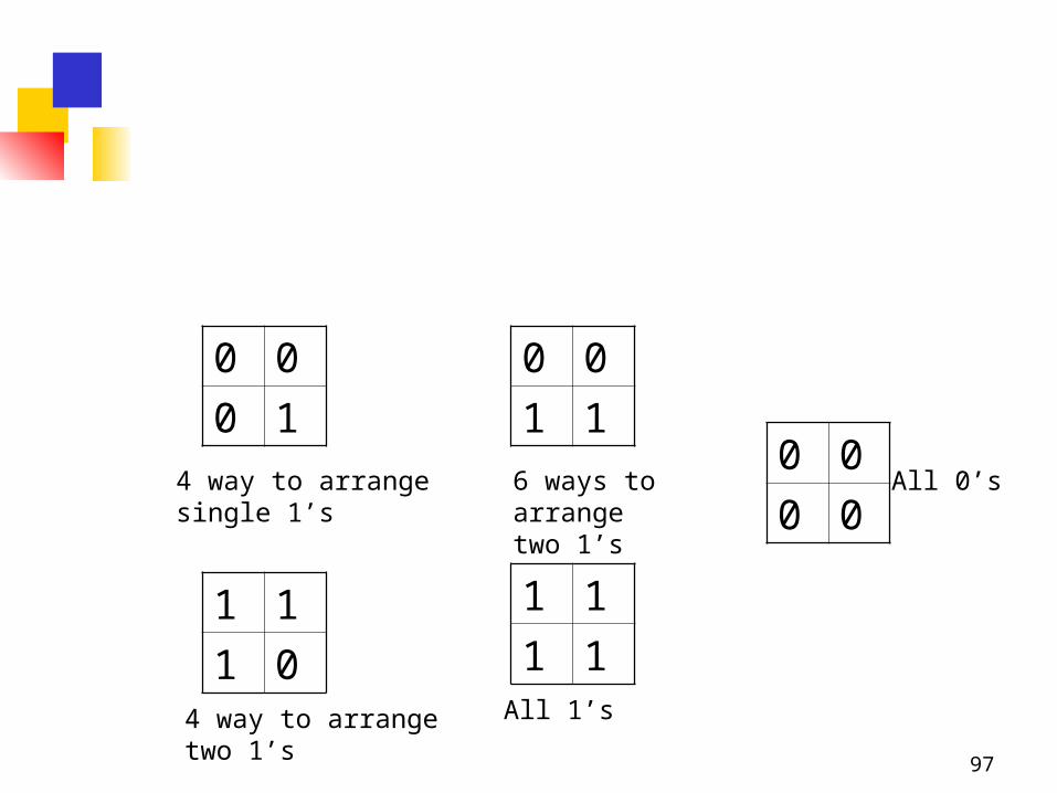
0 04 way to arrangesingle 1’s
6 ways to arrangetwo 1’s
4 way to arrangetwo 1’s
All 1’s
All 0’s

98
c
d
b
fg
e
F2
d
a (b c + b d) + a (e f +e g) a
b e
c d f g
0 1
0 1
0 1 0 1
0
1 0
1
0
1
0
1
F= a’ (b’ c + b d) + a (e’ f +e g)

99
D
Data
read/write Q
Q
0/1
0/1
0/1
0/1
0/1
0/1
0/1
0/1


![Abstract - Index terms - IJSER...model can be done using ASIC’s or FPGA’s. The latter is developed by the authors[4].The use of FPGA’s extends more flexibility to the design](https://cdn.vdocument.in/doc/165x107/5e4dee5581ffa45a463ef04f/abstract-index-terms-ijser-model-can-be-done-using-asicas-or-fpgaas.jpg)

