
1
Fairchild Smart Power Products for Automotive Business
June 2006
Fairchild SemiconductorThe Leader in Optimizing System Power

2
Smart Power Applications
Ignition Switch On Plug
Mirror Folding/Unfolding
Interior Heating & Cooling Fan Control
Power Window
Sunroof control
Electronic Wiper Motor Control
Radiator Fan Motor Control
Electronic Headlamp Control
Electronic Seat Positioning Controls
+
3
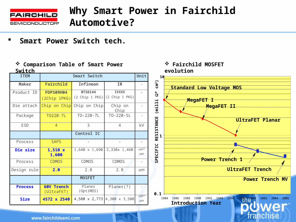
Why Smart Power in Fairchild Automotive?
Smart Power Switch tech.
Fairchild MOSFET evolution
Introduction Year
SP
EC
IFIC
RE
SIS
TA
NC
E (
mill
i *
cm2)
0.1
1
10
1984 1986 1988 1990 1992 1994 1996 1998 2000 2002 2004 2006
MegaFET IMegaFET II
Standard Low Voltage MOS
Power Trench 1
UltraFET Planar
UltraFET Trench
Power Trench MV
um*
um2,330x 1,4601,640 x 1,6901,510 x 1,600Die size
-CDMOS CDMOS CDMOSProcess
um2.82.82.0Design rule
-IXXXX
(2 Chip 1 PKG)
BTS6144
(2 Chip 1 PKG)
FDPS09H04
(2Chip 1PKG)
Product ID
-IRInfineonFairchildMaker
kV434ESD
Control IC
-Chip on ChipChip on ChipChip on ChipDie attach
-TO-220-5LTO-220-7LTO220-7LPackage
MOSFET
4,300 x 3,500
Planer(?)
-
60V Trench (UltraFET)
SAP5
Smart Switch
-Planer (OptiMOS)Process
um*
um4,580 x 2,773Size
-
Unit
-Process
ITEM
4572 x 2540
Comparison Table of Smart Power Switch
4
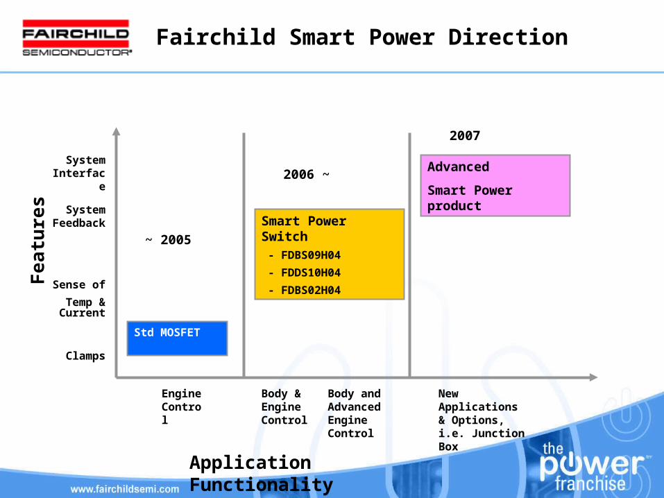
Fairchild Smart Power Direction
Std MOSFET
Smart Power Switch - FDBS09H04
- FDDS10H04
- FDBS02H04
Advanced
Smart Power product
Application Functionality
Clamps
Sense of
Temp & Current
System Feedback
System Interface
Fe
atu
res
~ 2005
2007
2006 ~
Engine Control
Body & Engine Control
Body and Advanced Engine Control
New Applications & Options, i.e. Junction Box

5
Fairchild High Side Switch Roadmap
FDDS10H04,
10 mOhm, 40V
Ultra Trench FET
FDBS02H04
2.4 mOhm, 40V
Power Trench FET 4th
FDMS0XH04 Series
2.4 ~ mOhm
PQFN Package
Serial Interface
FDBS09H04,
9 mOhm, 40V
Ultra Trench FET
2007 2008 2009
Robust High performance High configuration tech. System communication Complexity
2006
6
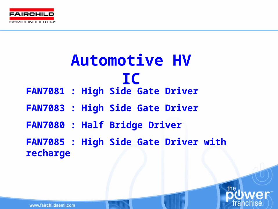
Automotive HV IC
FAN7081 : High Side Gate Driver
FAN7083 : High Side Gate Driver
FAN7080 : Half Bridge Driver
FAN7085 : High Side Gate Driver with recharge

7
FAN7081 High Side Gate DriverHigh Side Gate Driver
Code DCode D
Development ScheduleDevelopment Schedule
FeaturesFeatures
TechnicalTechnicalAnalysisAnalysis
Key Application Common-rail Piezo Valve in Injector Driver
Competitors IR2118
Package SOIC-8
BLOCK DIAGRAMBLOCK DIAGRAM
PULSE GEN
UV
DETECT
PULSEFILTER
R
R
S
Q
HV Level Shift
IN
VB
HO
VS
VCC
COM
UV
DETECT
•600V high side gate driver
•Floating channel designed for bootstrap operation
•Allowable negative transient is –9.8V @Vcc=15V
•High dV/dt immunity.[50V/ns]
•Gate drive supply range from 10V to 20V
•Under-voltage lockout
•CMOS Schmitt-triggered inputs with pull-up
•High side output out of phase with input
•120 / 110ns turn-on/ turn-off time
•250mA / 500mA source / sink current
•Operating temp : -40 C ~ 125 C
Start ER Sample Final Sample Code S2006-08-30
8
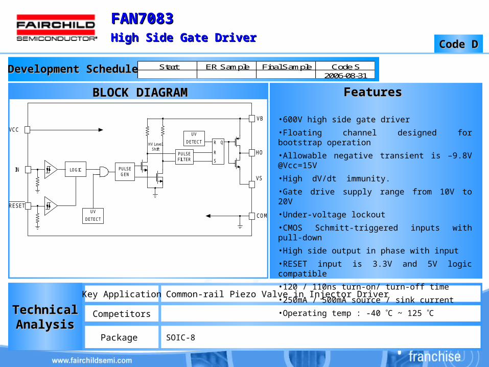
FAN7083FAN7083High Side Gate DriverHigh Side Gate Driver
Code DCode D
Development ScheduleDevelopment Schedule
FeaturesFeatures
TechnicalTechnicalAnalysisAnalysis
Key Application Common-rail Piezo Valve in Injector Driver
Competitors
Package SOIC-8
BLOCK DIAGRAMBLOCK DIAGRAM
Start ER Sample Final Sample Code S2006-08-31
•600V high side gate driver
•Floating channel designed for bootstrap operation
•Allowable negative transient is –9.8V @Vcc=15V
•High dV/dt immunity.
•Gate drive supply range from 10V to 20V
•Under-voltage lockout
•CMOS Schmitt-triggered inputs with pull-down
•High side output in phase with input
•RESET input is 3.3V and 5V logic compatible
•120 / 110ns turn-on/ turn-off time
•250mA / 500mA source / sink current
•Operating temp : -40 C ~ 125 C
PULSE GEN
UV
DETECT
UV
DETECT
PULSEFILTER
R
R
S
QHV Level Shift
IN
RESET
VB
HO
VS
COM
VCC
LOGIC
9
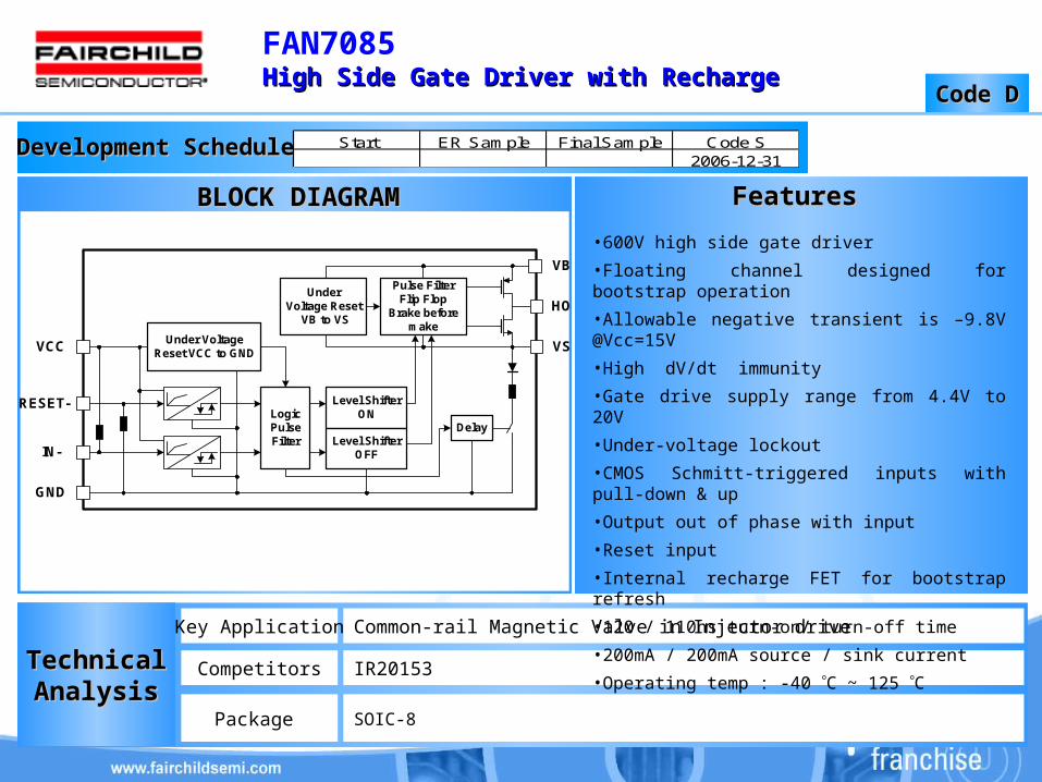
FAN7085 High Side Gate Driver with RechargeHigh Side Gate Driver with Recharge
Code DCode D
Development ScheduleDevelopment Schedule
FeaturesFeatures
TechnicalTechnicalAnalysisAnalysis
Key Application Common-rail Magnetic Valve in Injector drive
Competitors IR20153
Package SOIC-8
BLOCK DIAGRAMBLOCK DIAGRAM
Start ER Sample Final Sample Code S2006-12-31
•600V high side gate driver
•Floating channel designed for bootstrap operation
•Allowable negative transient is –9.8V @Vcc=15V
•High dV/dt immunity
•Gate drive supply range from 4.4V to 20V
•Under-voltage lockout
•CMOS Schmitt-triggered inputs with pull-down & up
•Output out of phase with input
•Reset input
•Internal recharge FET for bootstrap refresh
•120 / 110ns turn-on/ turn-off time
•200mA / 200mA source / sink current
•Operating temp : -40 C ~ 125 C
VCC Under Voltage Reset VCC to GND
Logic PulseFilter
Level ShifterON
Level ShifterOFF
Delay
Under Voltage Reset
VB to VS
Pulse FilterFlip Flop
Brake before make
RESET-
IN-
GND
VS
HO
VB
10
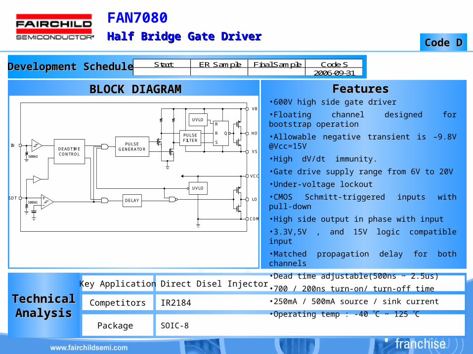
FAN7080
Half Bridge Gate DriverHalf Bridge Gate Driver Code DCode D
Development ScheduleDevelopment Schedule
FeaturesFeatures
TechnicalTechnicalAnalysisAnalysis
Key Application Direct Disel Injector
Competitors IR2184
Package SOIC-8
BLOCK DIAGRAMBLOCK DIAGRAM
Start ER Sample Final Sample Code S2006-09-31
•600V high side gate driver
•Floating channel designed for bootstrap operation
•Allowable negative transient is –9.8V @Vcc=15V
•High dV/dt immunity.
•Gate drive supply range from 6V to 20V
•Under-voltage lockout
•CMOS Schmitt-triggered inputs with pull-down
•High side output in phase with input
•3.3V,5V , and 15V logic compatible input
•Matched propagation delay for both channels
•Dead time adjustable(500ns ~ 2.5us)
•700 / 200ns turn-on/ turn-off time
•250mA / 500mA source / sink current
•Operating temp : -40 C ~ 125 C
DEADTIMECONTROL
DELAY
PULSEGENERATOR
PULSEFILTER
UVLOR
R
S
Q
UVLO
VCC
COM
LO
VB
HO
VS
IN
SDT500kΩ
500kΩ
11
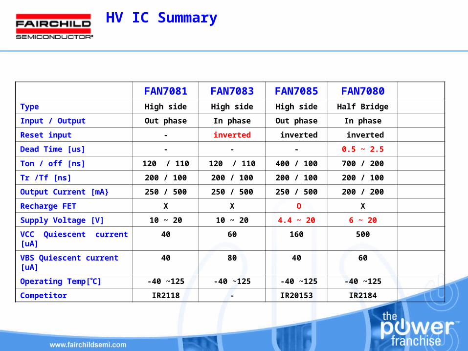
HV IC Summary
FAN7081 FAN7083 FAN7085 FAN7080
Type High side High side High side Half Bridge
Input / Output Out phase In phase Out phase In phase
Reset input - inverted inverted inverted
Dead Time [us] - - - 0.5 ~ 2.5
Ton / off [ns] 120 / 110 120 / 110 400 / 100 700 / 200
Tr /Tf [ns] 200 / 100 200 / 100 200 / 100 200 / 100
Output Current [mA} 250 / 500 250 / 500 250 / 500 200 / 200
Recharge FET X X O X
Supply Voltage [V] 10 ~ 20 10 ~ 20 4.4 ~ 20 6 ~ 20
VCC Quiescent current [uA] 40 60 160 500
VBS Quiescent current [uA] 40 80 40 60
Operating Temp[C] -40 ~125 -40 ~125 -40 ~125 -40 ~125
Competitor IR2118 - IR20153 IR2184
12
Fairchild High Side Switch
FDBS09H04FDDS10H04
13
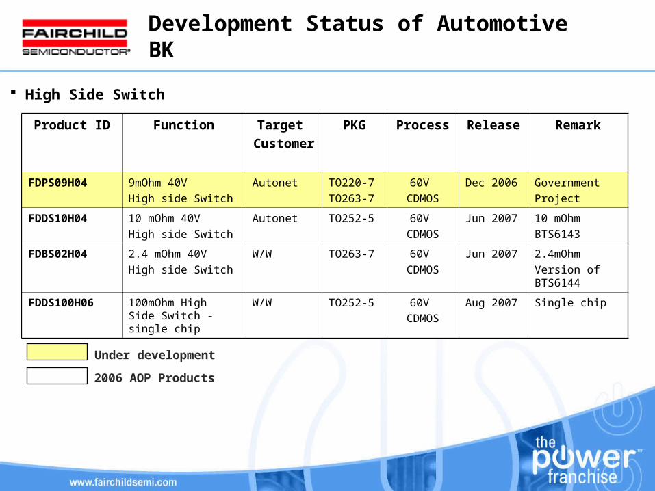
Development Status of Automotive BK
Product ID Function Target
Customer
PKG Process Release Remark
FDPS09H04 9mOhm 40V
High side Switch
Autonet TO220-7
TO263-7
60V
CDMOS
Dec 2006 Government
Project
FDDS10H04 10 mOhm 40V
High side Switch
Autonet TO252-5 60V
CDMOS
Jun 2007 10 mOhm
BTS6143
FDBS02H04 2.4 mOhm 40V
High side Switch
W/W TO263-7 60V
CDMOS
Jun 2007 2.4mOhm
Version of BTS6144
FDDS100H06 100mOhm High Side Switch - single chip
W/W TO252-5 60V
CDMOS
Aug 2007 Single chip
Under development
2006 AOP Products
High Side Switch
14
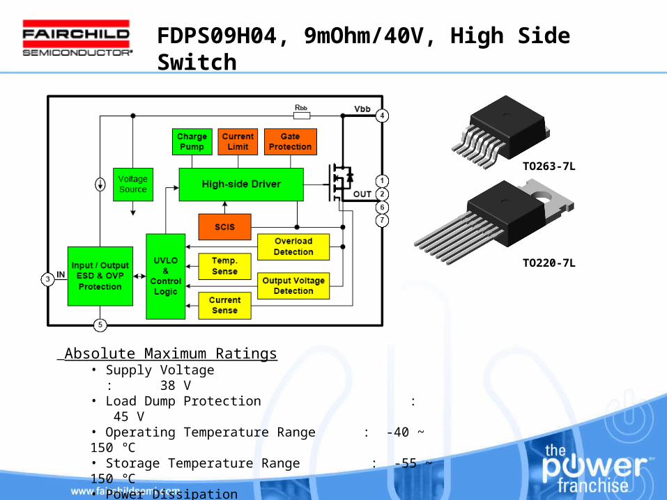
FDPS09H04, 9mOhm/40V, High Side Switch
Absolute Maximum Ratings• Supply Voltage : 38 V• Load Dump Protection : 45 V• Operating Temperature Range : -40 ~ 150 ℃• Storage Temperature Range : -55 ~ 150 ℃• Power Dissipation : 81 W• Electrostatic Discharge Capability : 4 KV
TO263-7L
TO220-7L
15
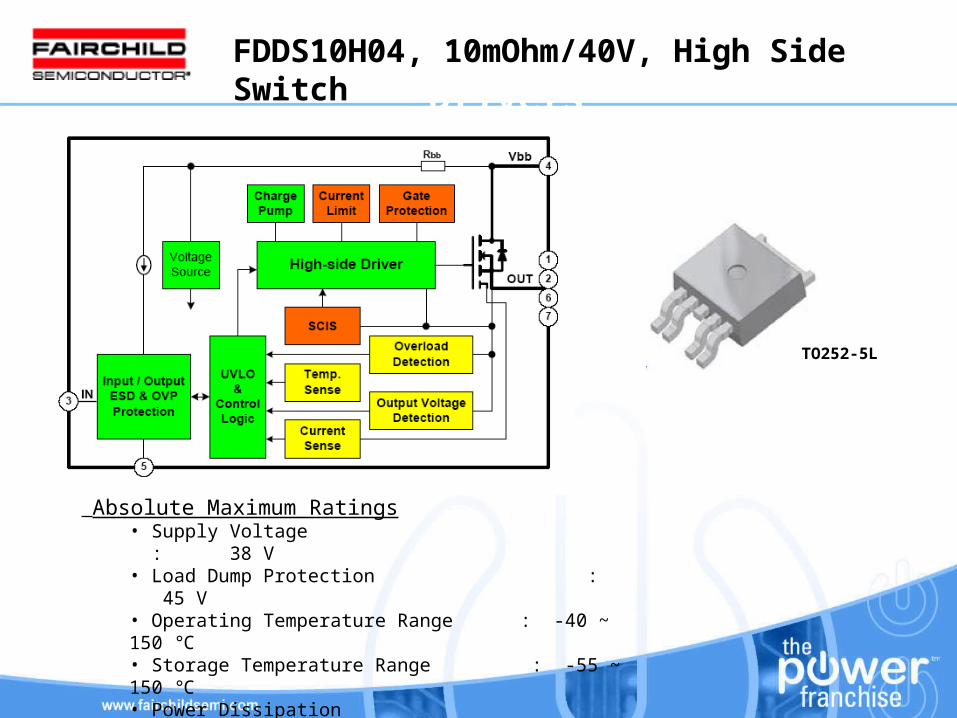
Competitive Smart High Side DriversFDDS10H04, 10mOhm/40V, High Side Switch
Absolute Maximum Ratings• Supply Voltage : 38 V• Load Dump Protection : 45 V• Operating Temperature Range : -40 ~ 150 ℃• Storage Temperature Range : -55 ~ 150 ℃• Power Dissipation : 59 W• Electrostatic Discharge Capability : 4 KV
TO252-5L
16
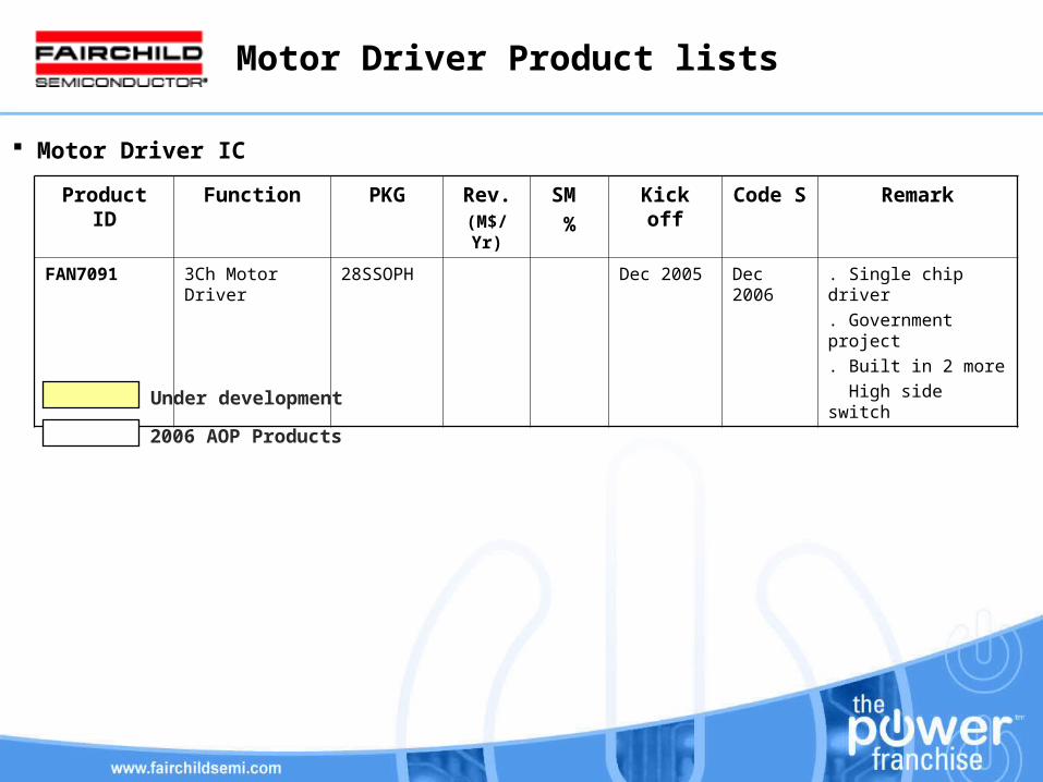
Motor Driver Product lists
Product ID Function PKG Rev.(M$/Yr)
SM
%
Kick off Code S Remark
FAN7091 3Ch Motor Driver 28SSOPH Dec 2005 Dec 2006 . Single chip driver
. Government project
. Built in 2 more
High side switch
Under development
2006 AOP Products
Motor Driver IC


