
Microcontrol lers
Data Sheet V 1.2, 2019-04
TC270 / TC275 / TC27732-Bit Single-Chip MicocontrollerDB-Step
32-Bi t Single-Chip Micocontrol ler
32-Bi tMicrocontroller

Edition 2019-04Published byInfineon Technologies AG81726 Munich, Germany© 2019 Infineon Technologies AGAll Rights Reserved.
Legal DisclaimerThe information given in this document shall in no event be regarded as a guarantee of conditions orcharacteristics. With respect to any examples or hints given herein, any typical values stated herein and/or anyinformation regarding the application of the device, Infineon Technologies hereby disclaims any and all warrantiesand liabilities of any kind, including without limitation, warranties of non-infringement of intellectual property rightsof any third party.
InformationFor further information on technology, delivery terms and conditions and prices, please contact the nearestInfineon Technologies Office (www.infineon.com)
WarningsDue to technical requirements, components may contain dangerous substances. For information on the types inquestion, please contact the nearest Infineon Technologies Office.Infineon Technologies components may be used in life-support devices or systems only with the express writtenapproval of Infineon Technologies, if a failure of such components can reasonably be expected to cause the failureof that life-support device or system or to affect the safety or effectiveness of that device or system. Life supportdevices or systems are intended to be implanted in the human body or to support and/or maintain and sustainand/or protect human life. If they fail, it is reasonable to assume that the health of the user or other persons maybe endangered.

TC270 / TC275 / TC277 DB-Step
Data Sheet 3 V 1.2 2019-04
Revision HistoryPage or Item Subjects (major changes since previous revision)V 1.2, 2019-04
The history is documented in the last chapter

TC270 / TC275 / TC277 DB-Step
Data Sheet 4 V 1.2 2019-04
Trademarks of Infineon Technologies AGAURIX™, C166™, CanPAK™, CIPOS™, CIPURSE™, EconoPACK™, CoolMOS™, CoolSET™,CORECONTROL™, CROSSAVE™, DAVE™, DI-POL™, EasyPIM™, EconoBRIDGE™, EconoDUAL™,EconoPIM™, EconoPACK™, EiceDRIVER™, eupec™, FCOS™, HITFET™, HybridPACK™, I²RF™,ISOFACE™, IsoPACK™, MIPAQ™, ModSTACK™, my-d™, NovalithIC™, OptiMOS™, ORIGA™,POWERCODE™; PRIMARION™, PrimePACK™, PrimeSTACK™, PRO-SIL™, PROFET™, RASIC™,ReverSave™, SatRIC™, SIEGET™, SINDRION™, SIPMOS™, SmartLEWIS™, SOLID FLASH™, TEMPFET™,thinQ!™, TRENCHSTOP™, TriCore™.
Other TrademarksAdvance Design System™ (ADS) of Agilent Technologies, AMBA™, ARM™, MULTI-ICE™, KEIL™,PRIMECELL™, REALVIEW™, THUMB™, µVision™ of ARM Limited, UK. AUTOSAR™ is licensed by AUTOSARdevelopment partnership. Bluetooth™ of Bluetooth SIG Inc. CAT-iq™ of DECT Forum. COLOSSUS™,FirstGPS™ of Trimble Navigation Ltd. EMV™ of EMVCo, LLC (Visa Holdings Inc.). EPCOS™ of Epcos AG.FLEXGO™ of Microsoft Corporation. FlexRay™ is licensed by FlexRay Consortium. HYPERTERMINAL™ ofHilgraeve Incorporated. IEC™ of Commission Electrotechnique Internationale. IrDA™ of Infrared DataAssociation Corporation. ISO™ of INTERNATIONAL ORGANIZATION FOR STANDARDIZATION. MATLAB™ ofMathWorks, Inc. MAXIM™ of Maxim Integrated Products, Inc. MICROTEC™, NUCLEUS™ of Mentor GraphicsCorporation. MIPI™ of MIPI Alliance, Inc. MIPS™ of MIPS Technologies, Inc., USA. muRata™ of MURATAMANUFACTURING CO., MICROWAVE OFFICE™ (MWO) of Applied Wave Research Inc., OmniVision™ ofOmniVision Technologies, Inc. Openwave™ Openwave Systems Inc. RED HAT™ Red Hat, Inc. RFMD™ RFMicro Devices, Inc. SIRIUS™ of Sirius Satellite Radio Inc. SOLARIS™ of Sun Microsystems, Inc. SPANSION™of Spansion LLC Ltd. Symbian™ of Symbian Software Limited. TAIYO YUDEN™ of Taiyo Yuden Co.TEAKLITE™ of CEVA, Inc. TEKTRONIX™ of Tektronix Inc. TOKO™ of TOKO KABUSHIKI KAISHA TA. UNIX™of X/Open Company Limited. VERILOG™, PALLADIUM™ of Cadence Design Systems, Inc. VLYNQ™ of TexasInstruments Incorporated. VXWORKS™, WIND RIVER™ of WIND RIVER SYSTEMS, INC. ZETEX™ of DiodesZetex Limited.Last Trademarks Update 2011-11-11

TC270 / TC275 / TC277 DB-Step
Data Sheet TOC-1 V 1.2, 2019-04
1 Summary of Features . . . . . . . . . . . . . . . . . . . . . . . . . . . . . . . . . . . . . . . . . . . . . . . . . . . . . . . . . . . . . 3
2 Package and Pinning Definitions . . . . . . . . . . . . . . . . . . . . . . . . . . . . . . . . . . . . . . . . . . . . . . . . . . . 72.1 TC275x Pin Definition and Functions: LQFP176 . . . . . . . . . . . . . . . . . . . . . . . . . . . . . . . . . . . . . . . . . 82.1.1 TC275x LQFP176 Package Variant Pin Configuration' . . . . . . . . . . . . . . . . . . . . . . . . . . . . . . . . . . . 92.1.2 Emergency Stop Function . . . . . . . . . . . . . . . . . . . . . . . . . . . . . . . . . . . . . . . . . . . . . . . . . . . . . . . . 632.1.3 Pull-Up/Pull-Down Reset Behavior of the Pins . . . . . . . . . . . . . . . . . . . . . . . . . . . . . . . . . . . . . . . . 642.2 TC277x Pin Definition and Functions: BGA292 . . . . . . . . . . . . . . . . . . . . . . . . . . . . . . . . . . . . . . . . . 652.2.1 TC277xBGA292 Package Variant Pin Configuration . . . . . . . . . . . . . . . . . . . . . . . . . . . . . . . . . . . . 662.2.2 Emergency Stop Function . . . . . . . . . . . . . . . . . . . . . . . . . . . . . . . . . . . . . . . . . . . . . . . . . . . . . . . 1362.2.3 Pull-Up/Pull-Down Reset Behavior of the Pins . . . . . . . . . . . . . . . . . . . . . . . . . . . . . . . . . . . . . . . 1372.3 TC270x Bare Die Pad Definition . . . . . . . . . . . . . . . . . . . . . . . . . . . . . . . . . . . . . . . . . . . . . . . . . . . 1382.3.1 Pad Openings . . . . . . . . . . . . . . . . . . . . . . . . . . . . . . . . . . . . . . . . . . . . . . . . . . . . . . . . . . . . . . . . 1512.3.2 Emergency Stop Function . . . . . . . . . . . . . . . . . . . . . . . . . . . . . . . . . . . . . . . . . . . . . . . . . . . . . . . 1512.3.3 Pull-Up/Pull-Down Reset Behavior of the Pins . . . . . . . . . . . . . . . . . . . . . . . . . . . . . . . . . . . . . . . 152
3 Electrical Specification . . . . . . . . . . . . . . . . . . . . . . . . . . . . . . . . . . . . . . . . . . . . . . . . . . . . . . . . . 1533.1 Parameter Interpretation . . . . . . . . . . . . . . . . . . . . . . . . . . . . . . . . . . . . . . . . . . . . . . . . . . . . . . . . . . 1533.2 Absolute Maximum Ratings . . . . . . . . . . . . . . . . . . . . . . . . . . . . . . . . . . . . . . . . . . . . . . . . . . . . . . . 1543.3 Pin Reliability in Overload . . . . . . . . . . . . . . . . . . . . . . . . . . . . . . . . . . . . . . . . . . . . . . . . . . . . . . . . . 1553.4 Operating Conditions . . . . . . . . . . . . . . . . . . . . . . . . . . . . . . . . . . . . . . . . . . . . . . . . . . . . . . . . . . . . 1583.5 5 V / 3.3 V switchable Pads . . . . . . . . . . . . . . . . . . . . . . . . . . . . . . . . . . . . . . . . . . . . . . . . . . . . . . . 1603.6 3.3 V only Pads . . . . . . . . . . . . . . . . . . . . . . . . . . . . . . . . . . . . . . . . . . . . . . . . . . . . . . . . . . . . . . . . . 1783.7 High performance LVDS Pads (LVDSH) . . . . . . . . . . . . . . . . . . . . . . . . . . . . . . . . . . . . . . . . . . . . . 1803.8 Medium performance LVDS Pads (LVDSM) . . . . . . . . . . . . . . . . . . . . . . . . . . . . . . . . . . . . . . . . . . 1843.9 VADC Parameters . . . . . . . . . . . . . . . . . . . . . . . . . . . . . . . . . . . . . . . . . . . . . . . . . . . . . . . . . . . . . . 1853.10 DSADC Parameters . . . . . . . . . . . . . . . . . . . . . . . . . . . . . . . . . . . . . . . . . . . . . . . . . . . . . . . . . . . . . 1913.11 MHz Oscillator . . . . . . . . . . . . . . . . . . . . . . . . . . . . . . . . . . . . . . . . . . . . . . . . . . . . . . . . . . . . . . . . . 1963.12 Back-up Clock . . . . . . . . . . . . . . . . . . . . . . . . . . . . . . . . . . . . . . . . . . . . . . . . . . . . . . . . . . . . . . . . . . 1973.13 Temperature Sensor . . . . . . . . . . . . . . . . . . . . . . . . . . . . . . . . . . . . . . . . . . . . . . . . . . . . . . . . . . . . . 1983.14 Power Supply Current . . . . . . . . . . . . . . . . . . . . . . . . . . . . . . . . . . . . . . . . . . . . . . . . . . . . . . . . . . . . 1993.14.1 Calculating the 1.3 V Current Consumption . . . . . . . . . . . . . . . . . . . . . . . . . . . . . . . . . . . . . . . . . 2023.15 Power-up and Power-down . . . . . . . . . . . . . . . . . . . . . . . . . . . . . . . . . . . . . . . . . . . . . . . . . . . . . . . 2033.15.1 External Supply Mode . . . . . . . . . . . . . . . . . . . . . . . . . . . . . . . . . . . . . . . . . . . . . . . . . . . . . . . . . . 2033.15.2 Single Supply Mode . . . . . . . . . . . . . . . . . . . . . . . . . . . . . . . . . . . . . . . . . . . . . . . . . . . . . . . . . . . . 2053.15.3 External Supply Mode . . . . . . . . . . . . . . . . . . . . . . . . . . . . . . . . . . . . . . . . . . . . . . . . . . . . . . . . . . 2073.15.4 Single Supply Mode . . . . . . . . . . . . . . . . . . . . . . . . . . . . . . . . . . . . . . . . . . . . . . . . . . . . . . . . . . . . 2093.16 Reset Timing . . . . . . . . . . . . . . . . . . . . . . . . . . . . . . . . . . . . . . . . . . . . . . . . . . . . . . . . . . . . . . . . . . . 2113.17 EVR . . . . . . . . . . . . . . . . . . . . . . . . . . . . . . . . . . . . . . . . . . . . . . . . . . . . . . . . . . . . . . . . . . . . . . . . . 2133.18 Phase Locked Loop (PLL) . . . . . . . . . . . . . . . . . . . . . . . . . . . . . . . . . . . . . . . . . . . . . . . . . . . . . . . . 2183.19 ERAY Phase Locked Loop (ERAY_PLL) . . . . . . . . . . . . . . . . . . . . . . . . . . . . . . . . . . . . . . . . . . . . . 2193.20 AC Specifications . . . . . . . . . . . . . . . . . . . . . . . . . . . . . . . . . . . . . . . . . . . . . . . . . . . . . . . . . . . . . . . 2203.21 JTAG Parameters . . . . . . . . . . . . . . . . . . . . . . . . . . . . . . . . . . . . . . . . . . . . . . . . . . . . . . . . . . . . . . . 2213.22 DAP Parameters . . . . . . . . . . . . . . . . . . . . . . . . . . . . . . . . . . . . . . . . . . . . . . . . . . . . . . . . . . . . . . . . 2233.23 ASCLIN SPI Master Timing . . . . . . . . . . . . . . . . . . . . . . . . . . . . . . . . . . . . . . . . . . . . . . . . . . . . . . . 2253.24 ASCLIN SPI Master Timing . . . . . . . . . . . . . . . . . . . . . . . . . . . . . . . . . . . . . . . . . . . . . . . . . . . . . . . 2293.25 QSPI Timings, Master and Slave Mode . . . . . . . . . . . . . . . . . . . . . . . . . . . . . . . . . . . . . . . . . . . . . . 2333.26 QSPI Timings, Master and Slave Mode . . . . . . . . . . . . . . . . . . . . . . . . . . . . . . . . . . . . . . . . . . . . . . 2383.27 MSC Timing 5 V Operation . . . . . . . . . . . . . . . . . . . . . . . . . . . . . . . . . . . . . . . . . . . . . . . . . . . . . . . . 2453.28 MSC Timing 3.3 V Operation . . . . . . . . . . . . . . . . . . . . . . . . . . . . . . . . . . . . . . . . . . . . . . . . . . . . . . 250
Table of Contents

TC270 / TC275 / TC277 DB-Step
Data Sheet 2 V 1.2 2019-04
3.29 Ethernet Interface (ETH) Characteristics . . . . . . . . . . . . . . . . . . . . . . . . . . . . . . . . . . . . . . . . . . . . . 2553.29.1 ETH Measurement Reference Points . . . . . . . . . . . . . . . . . . . . . . . . . . . . . . . . . . . . . . . . . . . . . . 2553.29.2 ETH Management Signal Parameters (ETH_MDC, ETH_MDIO) . . . . . . . . . . . . . . . . . . . . . . . . . 2563.29.3 ETH MII Parameters . . . . . . . . . . . . . . . . . . . . . . . . . . . . . . . . . . . . . . . . . . . . . . . . . . . . . . . . . . . 2573.29.4 ETH RMII Parameters . . . . . . . . . . . . . . . . . . . . . . . . . . . . . . . . . . . . . . . . . . . . . . . . . . . . . . . . . . 2583.30 E-Ray Parameters . . . . . . . . . . . . . . . . . . . . . . . . . . . . . . . . . . . . . . . . . . . . . . . . . . . . . . . . . . . . . . 2593.31 HSCT Parameters . . . . . . . . . . . . . . . . . . . . . . . . . . . . . . . . . . . . . . . . . . . . . . . . . . . . . . . . . . . . . . 2613.32 Inter-IC (I2C) Interface Timing . . . . . . . . . . . . . . . . . . . . . . . . . . . . . . . . . . . . . . . . . . . . . . . . . . . . . 2643.33 Flash Target Parameters . . . . . . . . . . . . . . . . . . . . . . . . . . . . . . . . . . . . . . . . . . . . . . . . . . . . . . . . . 2673.34 Package Outline . . . . . . . . . . . . . . . . . . . . . . . . . . . . . . . . . . . . . . . . . . . . . . . . . . . . . . . . . . . . . . . . 2703.34.1 Package Parameters . . . . . . . . . . . . . . . . . . . . . . . . . . . . . . . . . . . . . . . . . . . . . . . . . . . . . . . . . . . 2713.34.2 TC270 Carrier Tape . . . . . . . . . . . . . . . . . . . . . . . . . . . . . . . . . . . . . . . . . . . . . . . . . . . . . . . . . . . . 2713.35 Quality Declarations . . . . . . . . . . . . . . . . . . . . . . . . . . . . . . . . . . . . . . . . . . . . . . . . . . . . . . . . . . . . . 273
4 History . . . . . . . . . . . . . . . . . . . . . . . . . . . . . . . . . . . . . . . . . . . . . . . . . . . . . . . . . . . . . . . . . . . . . . . 2744.1 Changes from version version 0.6 to 0.7 . . . . . . . . . . . . . . . . . . . . . . . . . . . . . . . . . . . . . . . . . . . . . 2744.2 Changes from version version 0.7 to 1.0 . . . . . . . . . . . . . . . . . . . . . . . . . . . . . . . . . . . . . . . . . . . . . 2814.3 Changes from version version 1.0 to 1.1 . . . . . . . . . . . . . . . . . . . . . . . . . . . . . . . . . . . . . . . . . . . . . 2844.4 Changes from version version 1.1 to 1.2 . . . . . . . . . . . . . . . . . . . . . . . . . . . . . . . . . . . . . . . . . . . . . 284

TC270 / TC275 / TC277 DB-Step
Summary of Features
Data Sheet 3 V 1.2 2019-04
1 Summary of FeaturesThe TC27x product family has the following features:• High Performance Microcontroller with three CPU cores• Two 32-bit super-scalar TriCore CPUs (TC1.6P), each having the following features:
– Superior real-time performance– Strong bit handling– Fully integrated DSP capabilities– Multiply-accumulate unit able to sustain 2 MAC operations per cycle– Fully pipelined Floating point unit (FPU)– up to 200 MHz operation at full temperature range– up to 120 Kbyte Data Scratch-Pad RAM (DSPR) – up to 32 Kbyte Instruction Scratch-Pad RAM (PSPR) – 16 Kbyte Instruction Cache (ICACHE)– 8 Kbyte Data Cache (DCACHE)
• Power Efficient scalar TriCore CPU (TC1.6E), having the following features:– Binary code compatibility with TC1.6P– up to 200 MHz operation at full temperature range– up to 112 Kbyte Data Scratch-Pad RAM (DSPR) – up to 24 Kbyte Instruction Scratch-Pad RAM (PSPR) – 8 Kbyte Instruction Cache (ICACHE)– 0.125Kbyte Data Read Buffer (DRB)
• Lockstepped shadow cores for one TC1.6P and for TC1.6E • Multiple on-chip memories
– All embedded NVM and SRAM are ECC protected– up to 4 Mbyte Program Flash Memory (PFLASH) – up to 384 Kbyte Data Flash Memory (DFLASH) usable for EEPROM emulation– 32 Kbyte Memory (LMU)– BootROM (BROM)
• 64-Channel DMA Controller with safe data transfer• Sophisticated interrupt system (ECC protected)• High performance on-chip bus structure
– 64-bit Cross Bar Interconnect (SRI) giving fast parallel access between bus masters, CPUs and memories– 32-bit System Peripheral Bus (SPB) for on-chip peripheral and functional units– One bus bridge (SFI Bridge)
• Optional Hardware Security Module (HSM) on some variants • Safety Management Unit (SMU) handling safety monitor alarms• Memory Test Unit with ECC, Memory Initialization and MBIST functions (MTU)• Hardware I/O Monitor (IOM) for checking of digital I/O• Versatile On-chip Peripheral Units
– Four Asynchronous/Synchronous Serial Channels (ASCLIN) with hardware LIN support (V1.3, V2.0, V2.1 and J2602) up to 50 MBaud

TC270 / TC275 / TC277 DB-Step
Summary of Features
Data Sheet 4 V 1.2 2019-04
– Four Queued SPI Interface Channels (QSPI) with master and slave capability up to 50 Mbit/s– High Speed Serial Link (HSSL) for serial inter-processor communication up to 320 Mbit/s– Two serial Micro Second Bus interfaces (MSC) for serial port expansion to external power devices– One MultiCAN+ Module with 4 CAN nodes and 256 free assignable message objects for high efficiency
data handling via FIFO buffering and gateway data transfer – 10 Single Edge Nibble Transmission (SENT) channels for connection to sensors– One FlexRayTM module with 2 channels (E-Ray) supporting V2.1– One Generic Timer Module (GTM) providing a powerful set of digital signal filtering and timer functionality
to realize autonomous and complex Input/Output management– One Capture / Compare 6 module (Two kernels CCU60 and CCU61)– One General Purpose 12 Timer Unit (GPT120)– Three channel Peripheral Sensor Interface conforming to V1.3 (PSI5)– Peripheral Sensor Interface with Serial PHY (PSI5-S)– Optional Inter-Integrated Circuit Bus Interface (I2C) conforming to V2.1– Optional IEEE802.3 Ethernet MAC with RMII and MII interfaces (ETH)
• Versatile Successive Approximation ADC (VADC)– Cluster of 8 independent ADC kernels– Input voltage range from 0 V to 5.5V (ADC supply)
• Delta-Sigma ADC (DSADC)– Six channels
• Digital programmable I/O ports • On-chip debug support for OCDS Level 1 (CPUs, DMA, On Chip Buses)• multi-core debugging, real time tracing, and calibration• four/five wire JTAG (IEEE 1149.1) or DAP (Device Access Port) interface• Power Management System and on-chip regulators• Clock Generation Unit with System PLL and Flexray PLL• Embedded Voltage Regulator

TC270 / TC275 / TC277 DB-Step
Summary of Features
Data Sheet 5 V 1.2 2019-04
Ordering InformationThe ordering code for Infineon microcontrollers provides an exact reference to the required product. This orderingcode identifies:• The derivative itself, i.e. its function set, the temperature range, and the supply voltage• The package and the type of delivery.For the available ordering codes for the TC270 / TC275 / TC277 please refer to the “AURIX TC27xMicrocontrollers Variant Overview”, which summarizes all available variants.
Table 1-1 Overview of TC27x FunctionsFeatureCPU Core Type TC1.6P / TC1.6E
P Cores / Checker Cores / E Cores / Checker Cores
2 / 1 /1 / 1
Max. Freq. 200 MHz
FPU yes
Program Flash Size 4 Mbyte
Data Flash Size 384 Kbyte
Cache Instruction (P / E) 16 Kbyte / 8 Kbyte
Data (P / E) 8 Kbyte / -
SRAM Size TC1.6P(DSPR/PSPR)
120 Kbyte / 32 Kbyte 2)
Size TC1.6E (DSPR/PSPR) 112 Kbyte / 24 Kbyte 1) 2)
Size LMU 32 Kbyte
DMA Channels 64
ADC Channels 48 + 12
Converter 8
DSADC Channels 6
GTM TIM 4
TOM 3
ATOM / MCS 5 / 4
CMU / ICM 1 / 1
PSM 1
TBU 1
SPE 2
CMP / MON 1 / 1
BRC / DPLL 1 / 1
Timer GPT12 2
CCU6 2
STM Modules 3
FlexRay Modules 1
Channels 2

TC270 / TC275 / TC277 DB-Step
Summary of Features
Data Sheet 6 V 1.2 2019-04
CAN Nodes 4
Message Objects 256
QSPI Channels 4
ASCLIN Interfaces 4
I2C Interfaces 1
SENT Channels 10
PSI5 Modules 3
PSI5-S Modules 1
HSSL Channels 1
MSC Channels 2
Ethernet Channels 1
ASIL Level up to ASIL-D
FCE Modules 1
Safety support SMU 1
IOM 1
Security HSM 1
Embedded Voltage Regulator DCDC from 5 V / 3.3 V to 1.3 V Yes
Embedded Voltage Regulator LDO from 5 V / 3.3 V to 1.3 V Yes
Embedded Voltage Regulator LDO from 5 V to 3.3 V Yes
Low Power Feature Standby RAM Yes
Packages Type PG-LQFP-176-22 / LF-BGA-292-6 / LF-BGA-292-10
I/O Type 5 V CMOS / 3.3 V CMOS / LVDS
Tambient Range −40 … +125°C
1) Address range starts at lowest address defined in the User’s Manual. For reference see the Memory Maps chapter of the User’s Manual.
2) To ensure the processor cores are provided with a constant stream of instructions the Instruction Fetch Units will speculatively fetch instructions from the up to 64 bytes ahead of the current PC.If the current PC is within 64 bytes of the top of an instruction memory the Instruction Fetch Unit may attempt to speculatively fetch instruction from beyond the physical range. This may then lead to error conditions and alarms being triggered by the bus and memory systems.It is therefore recommended that the upper 64 bytes of any memory be unused for instruction storage.
Table 1-1 Overview of TC27x Functions (cont’d)Feature

TC270 / TC275 / TC277 DB-Step
Package and Pinning Definitions
Data Sheet 7 V 1.2 2019-04
2 Package and Pinning DefinitionsThis chapter gives a pinning of the different packages of the TC270 / TC275 / TC277.

TC270 / TC275 / TC277 DB-Step
Package and Pinning DefinitionsTC275x Pin Definition and Functions:
Data Sheet 8 V 1.2 2019-04
2.1 TC275x Pin Definition and Functions: LQFP176Figure 2-1 is showing the TC275x Logic Symbol for the package variant: QFP176.
Figure 2-1 TC275x Logic Symbol for the package variant LQFP176.
TC27x
P02.0P02.1P02.2P02.3P02.4P02.5P02.6P02.7P02.8
VDD/VDDSB
P00.0P00.1P00.2P00.3P00.4P00.5P00.6P00.7P00.8P00.9
P00.10P00.11P00.12
VDDV EXT
V AREF2
VAGND 2
AN47AN46AN45AN44AN39AN38AN37AN36AN35AN33AN32AN29AN28AN27AN26AN25AN24
123456789
1011121314151617181920212223242526272829303132333435363738394041424344
45 46 47 48 49 50 51 52 53 54 55 56 57 58 59 60 61 62 63 64 65 66 67 68 69 70 71 72 73 74 75 76 77 78 79 80 81 82 83 84 85 86 87 88
132131130129128127126125124123122121120119118117116115114113112111110109108107106105104103102101100
9998979695949392919089
176
175
174
173
172
171
170
169
168
167
166
165
164
163
162
161
160
159
158
157
156
155
154
153
152
151
150
149
148
147
146
145
144
143
142
141
140
139
138
137
136
135
134
133
AN21
AN20
AN19
AN18
AN17
AN16
VAG
ND1
V ARE
F1
V SS
M
VDD
M
AN13
AN12
AN11
AN10
AN8
AN7
AN6
AN5
AN4
AN3
AN2
AN1
AN0
V DD
V EX
TP
33.0
P33
.1P
33.2
P33
.3P
33.4
P33
.5P
33.6
P33
.7P
33.8
P33
.9P3
3.10
P33.
11P3
3.12
P33.
13V G
ATE1
N/ P
32.0
VG
ATE1
PP
32.2
P32
.3P
32.4
P20.14P20.13P20.12P20.11P20.10P20.9P20.8P20.7P20.6VDD
ESR0PORSTESR1P20.3P20.2 / TESTMODEP20.1P20.0TCKTRSTP21.7 / TDOTMSP21.6 / TDIP21.5P21.4P21.3P21.2P21.1P21.0VDDP 3
XTAL2XTAL1VSSVDD
VEXT
P22.3P22.2P22.1P22.0P23.5P23.4P23.3P23.2P23.1P23.0
P10.
8P1
0.7
P10.
6P1
0.5
P10.
4P1
0.3
P10.
2P1
0.1
P10.
0P1
1.12
P11.
11P1
1.10
VFL
EX
P11.
9P1
1.6
P11.
3P1
1.2
P13.
3P1
3.2
P13.
1P1
3.0
V DD
FL3
V DD
P3V E
XT
P14.
10P1
4.9
P14.
8P1
4.7
P14.
6P1
4.5
P14.
4P1
4.3
P14.
2P1
4.1
P14.
0P1
5.8
P15.
7P1
5.6
P15.
5P1
5.4
P15.
3P1
5.2
P15.
1P1
5.0

TC270 / TC275 / TC277 DB-Step
Package and Pinning DefinitionsTC275x Pin Definition and Functions:
Data Sheet 9 V 1.2 2019-04
2.1.1 TC275x LQFP176 Package Variant Pin Configuration'
Table 2-1 Port 00 FunctionsPin Symbol Ctrl Type Function11 P00.0 I MP /
PU1 /VEXT
General-purpose inputTIN9 GTM inputCTRAPA CCU61 inputT12HRE CCU60 inputINJ00 MSC0 inputCIFD9 CIF inputP00.0 O0 General-purpose outputTOUT9 O1 GTM outputASCLK3 O2 ASCLIN3 outputATX3 O3 ASCLIN3 output– O4 ReservedTXDCAN1 O5 CAN node 1 output– O6 ReservedCOUT63 O7 CCU60 outputETHMDIOA HWOU
TETH input/output
12 P00.1 I LP /PU1 /VEXT
General-purpose inputTIN10 GTM inputARX3E ASCLIN3 inputRXDCAN1D CAN node 1 inputPSIRX0A PSI5 inputSENT0B SENT inputCC60INB CCU60 inputCC60INA CCU61 inputDSCIN5A DSADC channel 5 input ADS5NA DSADC negative analog input of channel 5, pin AVADCG7.5 VADC analog input channel 5 of group 7CIFD10 CIF inputP00.1 O0 General-purpose outputTOUT10 O1 GTM outputATX3 O2 ASCLIN3 output– O3 ReservedDSCOUT5 O4 DSADC channel 5 output– O5 ReservedSPC0 O6 SENT outputCC60 O7 CCU61 output

TC270 / TC275 / TC277 DB-Step
Package and Pinning DefinitionsTC275x Pin Definition and Functions:
Data Sheet 10 V 1.2 2019-04
13 P00.2 I LP /PU1 /VEXT
General-purpose inputTIN11 GTM inputSENT1B SENT inputDSDIN5A DSADC channel 5 input ADS5PA DSADC positive analog input of channel 5, pin AVADCG7.4 VADC analog input channel 4 of group 7CIFD11 CIF inputP00.2 O0 General-purpose outputTOUT11 O1 GTM outputASCLK3 O2 ASCLIN3 output– O3 ReservedPSITX0 O4 PSI5 outputTXDCAN3 O5 CAN node 3 output– O6 ReservedCOUT60 O7 CCU61 output
14 P00.3 I LP /PU1 /VEXT
General-purpose inputTIN12 GTM inputRXDCAN3A CAN node 3 inputPSIRX1A PSI5 inputPSISRXA PSI5-S inputSENT2B SENT inputCC61INB CCU60 inputCC61INA CCU61 inputDSCIN3A DSADC channel 3 input AVADCG7.3 VADC analog input channel 3 of group 7DSITR5F DSADC channel 5 input FCIFD12 CIF inputP00.3 O0 General-purpose outputTOUT12 O1 GTM outputASLSO3 O2 ASCLIN3 output– O3 ReservedDSCOUT3 O4 DSADC channel 3 output– O5 ReservedSPC2 O6 SENT outputCC61 O7 CCU61 output
Table 2-1 Port 00 Functions (cont’d)Pin Symbol Ctrl Type Function

TC270 / TC275 / TC277 DB-Step
Package and Pinning DefinitionsTC275x Pin Definition and Functions:
Data Sheet 11 V 1.2 2019-04
15 P00.4 I LP /PU1 /VEXT
General-purpose inputTIN13 GTM inputREQ7 SCU inputSENT3B SENT inputDSDIN3A DSADC channel 3 input ADSSGNA DSADC inputVADCG7.2 VADC analog input channel 2 of group 7 (MD)CIFD13 CIF inputP00.4 O0 General-purpose outputTOUT13 O1 GTM outputPSISTX O2 PSI5-S output– O3 ReservedPSITX1 O4 PSI5 outputVADCG4BFL0 O5 VADC outputSPC3 O6 SENT outputCOUT61 O7 CCU61 output
16 P00.5 I LP /PU1 /VEXT
General-purpose inputTIN14 GTM inputPSIRX2A PSI5 inputSENT4B SENT inputCC62INB CCU60 inputCC62INA CCU61 inputDSCIN2A DSADC channel 2 input AVADCG7.1 VADC analog input channel 1 of group 7 (MD)CIFD14 CIF inputP00.5 O0 General-purpose outputTOUT14 O1 GTM outputDSCGPWMN O2 DSADC output– O3 ReservedDSCOUT2 O4 DSADC channel 2 outputVADCG4BFL1 O5 VADC outputSPC4 O6 SENT outputCC62 O7 CCU61 output
Table 2-1 Port 00 Functions (cont’d)Pin Symbol Ctrl Type Function

TC270 / TC275 / TC277 DB-Step
Package and Pinning DefinitionsTC275x Pin Definition and Functions:
Data Sheet 12 V 1.2 2019-04
17 P00.6 I LP /PU1 /VEXT
General-purpose inputTIN15 GTM inputSENT5B SENT inputDSDIN2A DSADC channel 2 input AVADCG7.0 VADC analog input channel 0 of group 7DSITR4F DSADC channel 4 input FCIFD15 CIF inputP00.6 O0 General-purpose outputTOUT15 O1 GTM outputDSCGPWMP O2 DSADC outputVADCG4BFL2 O3 VADC outputPSITX2 O4 PSI5 outputVADCEMUX10 O5 VADC outputSPC5 O6 SENT outputCOUT62 O7 CCU61 output
18 P00.7 I LP /PU1 /VEXT
General-purpose inputTIN16 GTM inputSENT6B SENT inputCC60INC CCU61 inputCCPOS0A CCU61 inputT12HRB CCU60 inputT2INA GPT120 inputDSCIN4A DSADC channel 4 input ADS4NA DSADC negative analog input of channel 4, pin AVADCG6.5 VADC analog input channel 5 of group 6CIFCLK CIF inputP00.7 O0 General-purpose outputTOUT16 O1 GTM output– O2 ReservedVADCG4BFL3 O3 VADC outputDSCOUT4 O4 DSADC channel 4 outputVADCEMUX11 O5 VADC outputSPC6 O6 SENT outputCC60 O7 CCU61 output
Table 2-1 Port 00 Functions (cont’d)Pin Symbol Ctrl Type Function

TC270 / TC275 / TC277 DB-Step
Package and Pinning DefinitionsTC275x Pin Definition and Functions:
Data Sheet 13 V 1.2 2019-04
19 P00.8 I LP /PU1 /VEXT
General-purpose inputTIN17 GTM inputSENT7B SENT inputCC61INC CCU61 inputCCPOS1A CCU61 inputT13HRB CCU60 inputT2EUDA GPT120 inputDSDIN4A DSADC channel 4 input ADS4PA DSADC channel 4 input AVADCG6.4 VADC analog input channel 4 of group 6CIFVSNC CIF inputP00.8 O0 General-purpose outputTOUT17 O1 GTM outputSLSO36 O2 QSPI3 output– O3 Reserved– O4 ReservedVADCEMUX12 O5 VADC outputSPC7 O6 SENT outputCC61 O7 CCU61 output
Table 2-1 Port 00 Functions (cont’d)Pin Symbol Ctrl Type Function

TC270 / TC275 / TC277 DB-Step
Package and Pinning DefinitionsTC275x Pin Definition and Functions:
Data Sheet 14 V 1.2 2019-04
20 P00.9 I LP /PU1 /VEXT
General-purpose inputTIN18 GTM inputSENT8B SENT inputCC62INC CCU61 inputCCPOS2A CCU61 inputT13HRC CCU60 inputT12HRC CCU60 inputT4EUDA GPT120 inputDSCIN1A DSADC channel 1 input AVADCG6.3 VADC analog input channel 3 of group 6DSITR3F DSADC channel 3 input FCIFHSNC CIF inputP00.9 O0 General-purpose outputTOUT18 O1 GTM outputSLSO37 O2 QSPI3 outputARTS3 O3 ASCLIN3 outputDSCOUT1 O4 DSADC channel 1 output– O5 ReservedSPC8 O6 SENT outputCC62 O7 CCU61 output
21 P00.10 I LP /PU1 /VEXT
General-purpose inputTIN19 GTM inputSENT9B SENT inputDSDIN1A DSADC channel 1 input AVADCG6.2 VADC analog input channel 2 of group 6 (MD)P00.10 O0 General-purpose outputTOUT19 O1 GTM output– O2 Reserved– O3 Reserved– O4 Reserved– O5 ReservedSPC9 O6 SENT outputCOUT63 O7 CCU61 output
Table 2-1 Port 00 Functions (cont’d)Pin Symbol Ctrl Type Function

TC270 / TC275 / TC277 DB-Step
Package and Pinning DefinitionsTC275x Pin Definition and Functions:
Data Sheet 15 V 1.2 2019-04
22 P00.11 I LP /PU1 /VEXT
General-purpose inputTIN20 GTM inputCTRAPA CCU60 inputT12HRE CCU61 inputDSCIN0A DSADC channel 0 input AVADCG6.1 VADC analog input channel 1 of group 6 (MD)P00.11 O0 General-purpose outputTOUT20 O1 GTM output– O2 Reserved– O3 ReservedDSCOUT0 O4 DSADC channel 0 output– O5 Reserved– O6 Reserved– O7 Reserved
23 P00.12 I LP /PU1 /VEXT
General-purpose inputTIN21 GTM inputACTS3A ASCLIN3 inputDSDIN0A DSADC channel 0 input AVADCG6.0 VADC analog input channel 0 of group 6P00.12 O0 General-purpose outputTOUT21 O1 GTM output– O2 Reserved– O3 Reserved– O4 Reserved– O5 Reserved– O6 ReservedCOUT63 O7 CCU61 output
Table 2-1 Port 00 Functions (cont’d)Pin Symbol Ctrl Type Function

TC270 / TC275 / TC277 DB-Step
Package and Pinning DefinitionsTC275x Pin Definition and Functions:
Data Sheet 16 V 1.2 2019-04
Table 2-2 Port 02 FunctionsPin Symbol Ctrl Type Function1 P02.0 I MP+ /
PU1 / VEXT
General-purpose inputTIN0 GTM inputARX2G ASCLIN2 inputREQ6 SCU inputCC60INA CCU60 inputCC60INB CCU61 inputCIFD0 CIF inputP02.0 O0 General-purpose outputTOUT0 O1 GTM outputATX2 O2 ASCLIN2 outputSLSO31 O3 QSPI3 outputDSCGPWMN O4 DSADC outputTXDCAN0 O5 CAN node 0 outputTXDA O6 ERAY outputCC60 O7 CCU60 output
2 P02.1 I LP / PU1 / VEXT
General-purpose inputTIN1 GTM inputREQ14 SCU inputARX2B ASCLIN2 inputRXDCAN0A CAN node 0 inputRXDA2 ERAY inputCIFD1 CIF inputP02.1 O0 General-purpose outputTOUT1 O1 GTM output– O2 ReservedSLSO32 O3 QSPI3 outputDSCGPWMP O4 DSADC output– O5 Reserved– O6 ReservedCOUT60 O7 CCU60 output

TC270 / TC275 / TC277 DB-Step
Package and Pinning DefinitionsTC275x Pin Definition and Functions:
Data Sheet 17 V 1.2 2019-04
3 P02.2 I MP+ /PU1 /VEXT
General-purpose inputTIN2 GTM inputCC61INA CCU60 inputCC61INB CCU61 inputCIFD2 CIF inputP02.2 O0 General-purpose outputTOUT2 O1 GTM outputATX1 O2 ASCLIN1 outputSLSO33 O3 QSPI3 outputPSITX0 O4 PSI5 outputTXDCAN2 O5 CAN node 2 outputTXDB O6 ERAY outputCC61 O7 CCU60 output
4 P02.3 I LP /PU1 /VEXT
General-purpose inputTIN3 GTM inputARX1G ASCLIN1 inputRXDCAN2B CAN node 2 inputRXDB2 ERAY inputPSIRX0B PSI5 inputDSCIN5B DSADC channel 5 input BSDI11 MSC1 inputCIFD3 CIF inputP02.3 O0 General-purpose outputTOUT3 O1 GTM outputASLSO2 O2 ASCLIN2 outputSLSO34 O3 QSPI3 outputDSCOUT5 O4 DSADC channel 5 output– O5 Reserved– O6 ReservedCOUT61 O7 CCU60 output
Table 2-2 Port 02 Functions (cont’d)Pin Symbol Ctrl Type Function

TC270 / TC275 / TC277 DB-Step
Package and Pinning DefinitionsTC275x Pin Definition and Functions:
Data Sheet 18 V 1.2 2019-04
5 P02.4 I MP+ / PU1 /VEXT
General-purpose inputTIN4 GTM inputSLSI3A QSPI3 inputECTT1 TTCAN inputRXDCAN0D CAN node 0 inputCC62INA CCU60 inputCC62INB CCU61 inputDSDIN5B DSADC channel 5 input BSDA0A I2C0 inputCIFD4 CIF inputP02.4 O0 General-purpose outputTOUT4 O1 GTM outputASCLK2 O2 ASCLIN2 outputSLSO30 O3 QSPI3 outputPSISCLK O4 PSI5-S outputSDA0 O5 I2C0 outputTXENA O6 ERAY outputCC62 O7 CCU60 output
6 P02.5 I MP+ /PU1 /VEXT
General-purpose inputTIN5 GTM inputMRST3A QSPI3 inputECTT2 TTCAN inputPSIRX1B PSI5 inputPSISRXB PSI5-S inputSENT3C SENT inputDSCIN4B DSADC channel 4 input BSCL0A I2C0 inputCIFD5 CIF inputP02.5 O0 General-purpose outputTOUT5 O1 GTM outputTXDCAN0 O2 CAN node 0 outputMRST3 O3 QSPI3 outputDSCOUT4 O4 DSADC channel 4 outputSCL0 O5 I2C0 outputTXENB O6 ERAY outputCOUT62 O7 CCU60 output
Table 2-2 Port 02 Functions (cont’d)Pin Symbol Ctrl Type Function

TC270 / TC275 / TC277 DB-Step
Package and Pinning DefinitionsTC275x Pin Definition and Functions:
Data Sheet 19 V 1.2 2019-04
7 P02.6 I MP / PU1 /VEXT
General-purpose inputTIN6 GTM inputMTSR3A QSPI3 inputSENT2C SENT inputCC60INC CCU60 inputCCPOS0A CCU60 inputT12HRB CCU61 inputT3INA GPT120 inputCIFD6 CIF inputDSDIN4B DSADC channel 4 input BDSITR5E DSADC channel 5 input EP02.6 O0 General-purpose outputTOUT6 O1 GTM outputPSISTX O2 PSI5-S outputMTSR3 O3 QSPI3 outputPSITX1 O4 PSI5 outputVADCEMUX00 O5 VADC output– O6 ReservedCC60 O7 CCU60 output
Table 2-2 Port 02 Functions (cont’d)Pin Symbol Ctrl Type Function
TC270 / TC275 / TC277 DB-Step
Package and Pinning DefinitionsTC275x Pin Definition and Functions:
Data Sheet 20 V 1.2 2019-04
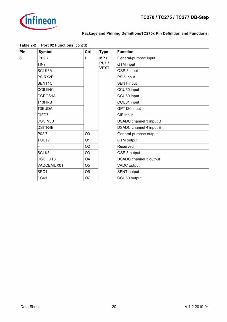
8 P02.7 I MP /PU1 /VEXT
General-purpose inputTIN7 GTM inputSCLK3A QSPI3 inputPSIRX2B PSI5 inputSENT1C SENT inputCC61INC CCU60 inputCCPOS1A CCU60 inputT13HRB CCU61 inputT3EUDA GPT120 inputCIFD7 CIF inputDSCIN3B DSADC channel 3 input BDSITR4E DSADC channel 4 input EP02.7 O0 General-purpose outputTOUT7 O1 GTM output– O2 ReservedSCLK3 O3 QSPI3 outputDSCOUT3 O4 DSADC channel 3 outputVADCEMUX01 O5 VADC outputSPC1 O6 SENT outputCC61 O7 CCU60 output
Table 2-2 Port 02 Functions (cont’d)Pin Symbol Ctrl Type Function

TC270 / TC275 / TC277 DB-Step
Package and Pinning DefinitionsTC275x Pin Definition and Functions:
Data Sheet 21 V 1.2 2019-04
9 P02.8 I LP / PU1 /VEXT
General-purpose inputTIN8 GTM inputSENT0C SENT inputCC62INC CCU60 inputCCPOS2A CCU60 inputT12HRC CCU61 inputT13HRC CCU61 inputT4INA GPT120 inputCIFD8 CIF inputDSDIN3B DSADC channel 3 input BDSITR3E DSADC channel 3 input EP02.8 O0 General-purpose outputTOUT8 O1 GTM outputSLSO35 O2 QSPI3 output– O3 ReservedPSITX2 O4 PSI5 outputVADCEMUX02 O5 VADC outputETHMDC O6 ETH outputCC62 O7 CCU60 output
Table 2-3 Port 10 FunctionsPin Symbol Ctrl Type Function168 P10.0 I LP /
PU1 /VEXT
General-purpose inputTIN102 GTM inputT6EUDB GPT120 inputP10.0 O0 General-purpose outputTOUT102 O1 GTM output– O2 ReservedSLSO110 O3 QSPI1 output– O4 ReservedVADCG6BFL0 O5 VADC output– O6 Reserved– O7 Reserved
Table 2-2 Port 02 Functions (cont’d)Pin Symbol Ctrl Type Function

TC270 / TC275 / TC277 DB-Step
Package and Pinning DefinitionsTC275x Pin Definition and Functions:
Data Sheet 22 V 1.2 2019-04
169 P10.1 I MP+ /PU1 /VEXT
General-purpose inputTIN103 GTM inputMRST1A QSPI1 inputT5EUDB GPT120 inputP10.1 O0 General-purpose outputTOUT103 O1 GTM outputMTSR1 O2 QSPI1 outputMRST1 O3 QSPI1 outputEN01 O4 MSC0 outputVADCG6BFL1 O5 VADC outputEND03 O6 MSC0 output– O7 Reserved
170 P10.2 I MP /PU1 /VEXT
General-purpose inputTIN104 GTM inputSCLK1A QSPI1 inputT6INB GPT120 inputREQ2 SCU inputRXDCAN2E CAN node 2 inputSDI01 MSC0 inputP10.2 O0 General-purpose outputTOUT104 O1 GTM output– O2 ReservedSCLK1 O3 QSPI1 outputEN00 O4 MSC0 outputVADCG6BFL2 O5 VADC outputEND02 O6 MSC0 output– O7 Reserved
Table 2-3 Port 10 Functions (cont’d)Pin Symbol Ctrl Type Function

TC270 / TC275 / TC277 DB-Step
Package and Pinning DefinitionsTC275x Pin Definition and Functions:
Data Sheet 23 V 1.2 2019-04
171 P10.3 I MP /PU1 /VEXT
General-purpose inputTIN105 GTM inputMTSR1A QSPI1 inputREQ3 SCU inputT5INB GPT120 inputP10.3 O0 General-purpose outputTOUT105 O1 GTM outputVADCG6BFL3 O2 VADC outputMTSR1 O3 QSPI1 outputEN00 O4 MSC0 outputEND02 O5 MSC0 outputTXDCAN2 O6 CAN node 2 output– O7 Reserved
172 P10.4 I MP+ /PU1 /VEXT
General-purpose inputTIN106 GTM inputMTSR1C QSPI1 inputCCPOS0C CCU60 inputT3INB GPT120 inputP10.4 O0 General-purpose outputTOUT106 O1 GTM output– O2 ReservedSLSO18 O3 QSPI1 outputMTSR1 O4 QSPI1 outputEN00 O5 MSC0 outputEND02 O6 MSC0 output– O7 Reserved
173 P10.5 I LP /PU1 /VEXT
General-purpose inputTIN107 GTM inputHWCFG4 SCU inputINJ01 MSC0 inputP10.5 O0 General-purpose outputTOUT107 O1 GTM outputATX2 O2 ASCLIN2 outputSLSO38 O3 QSPI3 outputSLSO19 O4 QSPI1 outputT6OUT O5 GPT120 outputASLSO2 O6 ASCLIN2 output- O7 Reserved
Table 2-3 Port 10 Functions (cont’d)Pin Symbol Ctrl Type Function

TC270 / TC275 / TC277 DB-Step
Package and Pinning DefinitionsTC275x Pin Definition and Functions:
Data Sheet 24 V 1.2 2019-04
174 P10.6 I LP /PU1 /VEXT
General-purpose inputTIN108 GTM inputARX2D ASCLIN2 inputMTSR3B QSPI3 inputHWCFG5 SCU inputP10.6 O0 General-purpose outputTOUT108 O1 GTM outputASCLK2 O2 ASCLIN2 outputMTSR3 O3 QSPI3 outputT3OUT O4 GPT120 output- O5 ReservedMRST1 O6 QSPI1 outputVADCG7BFL0 O7 VADC output
175 P10.7 I LP /PU1 /VEXT
General-purpose inputTIN109 GTM inputACTS2A ASCLIN2 inputMRST3B QSPI3 inputREQ4 SCU inputCCPOS1C CCU60 inputT3EUDB GPT120 inputP10.7 O0 General-purpose outputTOUT109 O1 GTM output– O2 ReservedMRST3 O3 QSPI3 outputVADCG7BFL1 O4 VADC output– O5 Reserved– O6 Reserved– O7 Reserved
Table 2-3 Port 10 Functions (cont’d)Pin Symbol Ctrl Type Function

TC270 / TC275 / TC277 DB-Step
Package and Pinning DefinitionsTC275x Pin Definition and Functions:
Data Sheet 25 V 1.2 2019-04
176 P10.8 I LP /PU1 /VEXT
General-purpose inputTIN110 GTM inputSCLK3B QSPI3 inputREQ5 SCU inputCCPOS2C CCU60 inputT4INB GPT120 inputP10.8 O0 General-purpose outputTOUT110 O1 GTM outputARTS2 O2 ASCLIN2 outputSCLK3 O3 QSPI3 output– O4 Reserved– O5 Reserved– O6 Reserved– O7 Reserved
Table 2-4 Port 11 FunctionsPin Symbol Ctrl Type Function160 P11.2 I MPR /
PU1 /VFLEX
General-purpose inputTIN95 GTM inputP11.2 O0 General-purpose outputTOUT95 O1 GTM outputEND03 O2 MSC0 outputSLSO05 O3 QSPI0 outputSLSO15 O4 QSPI1 outputEN01 O5 MSC0 outputETHTXD1 O6 ETH outputCOUT63 O7 CCU60 output
Table 2-3 Port 10 Functions (cont’d)Pin Symbol Ctrl Type Function

TC270 / TC275 / TC277 DB-Step
Package and Pinning DefinitionsTC275x Pin Definition and Functions:
Data Sheet 26 V 1.2 2019-04
161 P11.3 I MPR /PU1 /VFLEX
General-purpose inputTIN96 GTM inputMRST1B QSPI1 inputSDI03 MSC0 inputP11.3 O0 General-purpose outputTOUT96 O1 GTM output– O2 ReservedMRST1 O3 QSPI1 outputTXDA O4 ERAY output– O5 ReservedETHTXD0 O6 ETH outputCOUT62 O7 CCU60 output
162 P11.6 I MPR /PU1 /VFLEX
General-purpose inputTIN97 GTM inputSCLK1B QSPI1 inputP11.6 O0 General-purpose outputTOUT97 O1 GTM outputTXENB O2 ERAY outputSCLK1 O3 QSPI1 outputTXENA O4 ERAY outputFCLP0 O5 MSC0 outputETHTXEN O6 ETH outputCOUT61 O7 CCU60 output
163 P11.9 I MP+ /PU1 /VFLEX
General-purpose inputTIN98 GTM inputMTSR1B QSPI1 inputRXDA1 ERAY inputETHRXD1 ETH inputP11.9 O0 General-purpose outputTOUT98 O1 GTM output– O2 ReservedMTSR1 O3 QSPI1 output– O4 ReservedSOP0 O5 MSC0 output– O6 ReservedCOUT60 O7 CCU60 output
Table 2-4 Port 11 Functions (cont’d)Pin Symbol Ctrl Type Function
TC270 / TC275 / TC277 DB-Step
Package and Pinning DefinitionsTC275x Pin Definition and Functions:
Data Sheet 27 V 1.2 2019-04
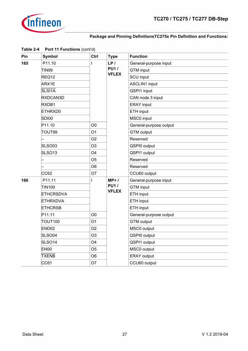
165 P11.10 I LP /PU1 /VFLEX
General-purpose inputTIN99 GTM inputREQ12 SCU inputARX1E ASCLIN1 inputSLSI1A QSPI1 inputRXDCAN3D CAN node 3 inputRXDB1 ERAY inputETHRXD0 ETH inputSDI00 MSC0 inputP11.10 O0 General-purpose outputTOUT99 O1 GTM output– O2 ReservedSLSO03 O3 QSPI0 outputSLSO13 O4 QSPI1 output– O5 Reserved– O6 ReservedCC62 O7 CCU60 output
166 P11.11 I MP+ /PU1 /VFLEX
General-purpose inputTIN100 GTM inputETHCRSDVA ETH inputETHRXDVA ETH inputETHCRSB ETH inputP11.11 O0 General-purpose outputTOUT100 O1 GTM outputEND02 O2 MSC0 outputSLSO04 O3 QSPI0 outputSLSO14 O4 QSPI1 outputEN00 O5 MSC0 outputTXENB O6 ERAY outputCC61 O7 CCU60 output
Table 2-4 Port 11 Functions (cont’d)Pin Symbol Ctrl Type Function

TC270 / TC275 / TC277 DB-Step
Package and Pinning DefinitionsTC275x Pin Definition and Functions:
Data Sheet 28 V 1.2 2019-04
167 P11.12 I MPR /PU1 /VFLEX
General-purpose inputTIN101 GTM inputETHREFCLK ETH inputETHTXCLKB ETH input
(Not for productive purposes)ETHRXCLKA ETH input
(Not for productive purposes)P11.12 O0 General-purpose outputTOUT101 O1 GTM outputATX1 O2 ASCLIN1 outputGTMCLK2 O3 GTM outputTXDB O4 ERAY outputTXDCAN3 O5 CAN node 3 outputEXTCLK1 O6 SCU outputCC60 O7 CCU60 output
Table 2-5 Port 13 FunctionsPin Symbol Ctrl Type Function156 P13.0 I LVDSM_N /
PU1 / VEXT
General-purpose inputTIN91 GTM inputP13.0 O0 General-purpose outputTOUT91 O1 GTM outputEND03 O2 MSC0 outputSCLK2N O3 QSPI2 output (LVDS)EN01 O4 MSC0 outputFCLN0 O5 MSC0 output (LVDS)FCLND0 O6 MSC0 output (LVDS)– O7 Reserved
157 P13.1 I LVDSM_P /PU1 / VEXT
General-purpose inputTIN92 GTM inputSCL0B I2C0 inputP13.1 O0 General-purpose outputTOUT92 O1 GTM output– O2 ReservedSCLK2P O3 QSPI2 output (LVDS)– O4 ReservedFCLP0 O5 MSC0 output (LVDS)SCL0 O6 I2C0 output– O7 Reserved
Table 2-4 Port 11 Functions (cont’d)Pin Symbol Ctrl Type Function
TC270 / TC275 / TC277 DB-Step
Package and Pinning DefinitionsTC275x Pin Definition and Functions:
Data Sheet 29 V 1.2 2019-04
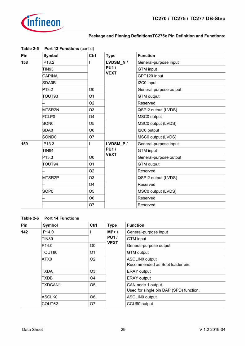
158 P13.2 I LVDSM_N /PU1 / VEXT
General-purpose inputTIN93 GTM inputCAPINA GPT120 inputSDA0B I2C0 inputP13.2 O0 General-purpose outputTOUT93 O1 GTM output– O2 ReservedMTSR2N O3 QSPI2 output (LVDS)FCLP0 O4 MSC0 outputSON0 O5 MSC0 output (LVDS)SDA0 O6 I2C0 outputSOND0 O7 MSC0 output (LVDS)
159 P13.3 I LVDSM_P /PU1 / VEXT
General-purpose inputTIN94 GTM inputP13.3 O0 General-purpose outputTOUT94 O1 GTM output– O2 ReservedMTSR2P O3 QSPI2 output (LVDS)– O4 ReservedSOP0 O5 MSC0 output (LVDS)– O6 Reserved– O7 Reserved
Table 2-6 Port 14 FunctionsPin Symbol Ctrl Type Function142 P14.0 I MP+ /
PU1 /VEXT
General-purpose inputTIN80 GTM inputP14.0 O0 General-purpose outputTOUT80 O1 GTM outputATX0 O2 ASCLIN0 output
Recommended as Boot loader pin.TXDA O3 ERAY outputTXDB O4 ERAY outputTXDCAN1 O5 CAN node 1 output
Used for single pin DAP (SPD) function.ASCLK0 O6 ASCLIN0 outputCOUT62 O7 CCU60 output
Table 2-5 Port 13 Functions (cont’d)Pin Symbol Ctrl Type Function

TC270 / TC275 / TC277 DB-Step
Package and Pinning DefinitionsTC275x Pin Definition and Functions:
Data Sheet 30 V 1.2 2019-04
143 P14.1 I MP /PU1 /VEXT
General-purpose inputTIN81 GTM inputREQ15 SCU inputARX0A ASCLIN0 input
Recommended as Boot loader pin.RXDCAN1B CAN node 1 input
Used for single pin DAP (SPD) function.RXDA3 ERAY inputRXDB3 ERAY inputEVRWUPA SCU inputP14.1 O0 General-purpose outputTOUT81 O1 GTM outputATX0 O2 ASCLIN0 output– O3 Reserved– O4 Reserved– O5 Reserved– O6 ReservedCOUT63 O7 CCU60 output
144 P14.2 I LP /PU1 /VEXT
General-purpose inputTIN82 GTM inputHWCFG2EVR13
SCU inputLatched at cold power on reset to decide EVR13 activation.
P14.2 O0 General-purpose outputTOUT82 O1 GTM outputATX2 O2 ASCLIN2 outputSLSO21 O3 QSPI2 output– O4 Reserved– O5 ReservedASCLK2 O6 ASCLIN2 output– O7 Reserved
Table 2-6 Port 14 Functions (cont’d)Pin Symbol Ctrl Type Function

TC270 / TC275 / TC277 DB-Step
Package and Pinning DefinitionsTC275x Pin Definition and Functions:
Data Sheet 31 V 1.2 2019-04
145 P14.3 I LP /PU1 /VEXT
General-purpose inputTIN83 GTM inputARX2A ASCLIN2 inputREQ10 SCU inputHWCFG3_BMI SCU inputSDI02 MSC0 inputP14.3 O0 General-purpose outputTOUT83 O1 GTM outputATX2 O2 ASCLIN2 outputSLSO23 O3 QSPI2 outputASLSO1 O4 ASCLIN1 outputASLSO3 O5 ASCLIN3 output– O6 Reserved– O7 Reserved
146 P14.4 I LP /PU1 /VEXT
General-purpose inputTIN84 GTM inputHWCFG6 SCU input
Latched at cold power on reset to decide default pad reset state (PU or HighZ).
P14.4 O0 General-purpose outputTOUT84 O1 GTM output– O2 Reserved– O3 Reserved– O4 Reserved– O5 Reserved– O6 Reserved– O7 Reserved
Table 2-6 Port 14 Functions (cont’d)Pin Symbol Ctrl Type Function

TC270 / TC275 / TC277 DB-Step
Package and Pinning DefinitionsTC275x Pin Definition and Functions:
Data Sheet 32 V 1.2 2019-04
147 P14.5 I MP+ /PU1 /VEXT
General-purpose inputTIN85 GTM inputHWCFG1EVR33
SCU inputLatched at cold power on reset to decide EVR33 activation.
P14.5 O0 General-purpose outputTOUT85 O1 GTM output– O2 Reserved– O3 Reserved– O4 Reserved– O5 ReservedTXDB O6 ERAY output– O7 Reserved
148 P14.6 I MP+ /PU1 /VEXT
General-purpose inputTIN86 GTM inputHWCFG0DCLDO
SCU inputIf EVR13 active, latched at cold power on reset to decide between LDO and SMPS mode.
P14.6 O0 General-purpose outputTOUT86 O1 GTM output– O2 ReservedSLSO22 O3 QSPI2 output– O4 Reserved– O5 ReservedTXENB O6 ERAY output– O7 Reserved
149 P14.7 I LP /PU1 /VEXT
General-purpose inputTIN87 GTM inputRXDB0 ERAY inputP14.7 O0 General-purpose outputTOUT87 O1 GTM outputARTS0 O2 ASCLIN0 outputSLSO24 O3 QSPI2 output– O4 Reserved– O5 Reserved– O6 Reserved– O7 Reserved
Table 2-6 Port 14 Functions (cont’d)Pin Symbol Ctrl Type Function

TC270 / TC275 / TC277 DB-Step
Package and Pinning DefinitionsTC275x Pin Definition and Functions:
Data Sheet 33 V 1.2 2019-04
150 P14.8 I LP /PU1 /VEXT
General-purpose inputTIN88 GTM inputARX1D ASCLIN1 inputRXDCAN2D CAN node 2 inputRXDA0 ERAY inputP14.8 O0 General-purpose outputTOUT88 O1 GTM output– O2 Reserved– O3 Reserved– O4 Reserved– O5 Reserved– O6 Reserved– O7 Reserved
151 P14.9 I MP+ /PU1 /VEXT
General-purpose inputTIN89 GTM inputACTS0A ASCLIN0 inputP14.9 O0 General-purpose outputTOUT89 O1 GTM outputEND03 O2 MSC0 outputEN01 O3 MSC0 output– O4 ReservedTXENB O5 ERAY outputTXENA O6 ERAY output– O7 Reserved
152 P14.10 I MP+ /PU1 /VEXT
General-purpose inputTIN90 GTM inputP14.10 O0 General-purpose outputTOUT90 O1 GTM outputEND02 O2 MSC0 outputEN00 O3 MSC0 outputATX1 O4 ASCLIN1 outputTXDCAN2 O5 CAN node 2 outputTXDA O6 ERAY output– O7 Reserved
Table 2-6 Port 14 Functions (cont’d)Pin Symbol Ctrl Type Function

TC270 / TC275 / TC277 DB-Step
Package and Pinning DefinitionsTC275x Pin Definition and Functions:
Data Sheet 34 V 1.2 2019-04
Table 2-7 Port 15 FunctionsPin Symbol Ctrl Type Function133 P15.0 I LP /
PU1 /VEXT
General-purpose inputTIN71 GTM inputP15.0 O0 General-purpose outputTOUT71 O1 GTM outputATX1 O2 ASCLIN1 outputSLSO013 O3 QSPI0 output– O4 ReservedTXDCAN2 O5 CAN node 2 outputASCLK1 O6 ASCLIN1 output– O7 Reserved
134 P15.1 I LP /PU1 /VEXT
General-purpose inputTIN72 GTM inputREQ16 SCU inputARX1A ASCLIN1 inputRXDCAN2A CAN node 2 inputSLSI2B QSPI2 inputEVRWUPB SCU inputP15.1 O0 General-purpose outputTOUT72 O1 GTM outputATX1 O2 ASCLIN1 outputSLSO25 O3 QSPI2 output– O4 Reserved– O5 Reserved– O6 Reserved– O7 Reserved
135 P15.2 I MP /PU1 /VEXT
General-purpose inputTIN73 GTM inputSLSI2A QSPI2 inputMRST2E QSPI2 inputP15.2 O0 General-purpose outputTOUT73 O1 GTM outputATX0 O2 ASCLIN0 outputSLSO20 O3 QSPI2 output– O4 ReservedTXDCAN1 O5 CAN node 1 outputASCLK0 O6 ASCLIN0 output– O7 Reserved

TC270 / TC275 / TC277 DB-Step
Package and Pinning DefinitionsTC275x Pin Definition and Functions:
Data Sheet 35 V 1.2 2019-04
136 P15.3 I MP /PU1 /VEXT
General-purpose inputTIN74 GTM inputARX0B ASCLIN0 inputSCLK2A QSPI2 inputRXDCAN1A CAN node 1 inputP15.3 O0 General-purpose outputTOUT74 O1 GTM outputATX0 O2 ASCLIN0 outputSCLK2 O3 QSPI2 outputEND03 O4 MSC0 outputEN01 O5 MSC0 output– O6 Reserved– O7 Reserved
137 P15.4 I MP /PU1 /VEXT
General-purpose inputTIN75 GTM inputMRST2A QSPI2 inputREQ0 SCU inputSCL0C I2C0 inputP15.4 O0 General-purpose outputTOUT75 O1 GTM outputATX1 O2 ASCLIN1 outputMRST2 O3 QSPI2 output– O4 Reserved– O5 ReservedSCL0 O6 I2C0 outputCC62 O7 CCU60 output
Table 2-7 Port 15 Functions (cont’d)Pin Symbol Ctrl Type Function

TC270 / TC275 / TC277 DB-Step
Package and Pinning DefinitionsTC275x Pin Definition and Functions:
Data Sheet 36 V 1.2 2019-04
138 P15.5 I MP /PU1 /VEXT
General-purpose inputTIN76 GTM inputARX1B ASCLIN1 inputMTSR2A QSPI2 inputREQ13 SCU inputSDA0C I2C0 inputP15.5 O0 General-purpose outputTOUT76 O1 GTM outputATX1 O2 ASCLIN1 outputMTSR2 O3 QSPI2 outputEND02 O4 MSC0 outputEN00 O5 MSC0 outputSDA0 O6 I2C0 outputCC61 O7 CCU60 output
139 P15.6 I MP /PU1 /VEXT
General-purpose inputTIN77 GTM inputMTSR2B QSPI2 inputP15.6 O0 General-purpose outputTOUT77 O1 GTM outputATX3 O2 ASCLIN3 outputMTSR2 O3 QSPI2 output– O4 ReservedSCLK2 O5 QSPI2 outputASCLK3 O6 ASCLIN3 outputCC60 O7 CCU60 output
140 P15.7 I MP /PU1 /VEXT
General-purpose inputTIN78 GTM inputARX3A ASCLIN3 inputMRST2B QSPI2 inputP15.7 O0 General-purpose outputTOUT78 O1 GTM outputATX3 O2 ASCLIN3 outputMRST2 O3 QSPI2 output– O4 Reserved– O5 Reserved– O6 ReservedCOUT60 O7 CCU60 output
Table 2-7 Port 15 Functions (cont’d)Pin Symbol Ctrl Type Function

TC270 / TC275 / TC277 DB-Step
Package and Pinning DefinitionsTC275x Pin Definition and Functions:
Data Sheet 37 V 1.2 2019-04
141 P15.8 I MP /PU1 /VEXT
General-purpose inputTIN79 GTM inputSCLK2B QSPI2 inputREQ1 SCU inputP15.8 O0 General-purpose outputTOUT79 O1 GTM output– O2 ReservedSCLK2 O3 QSPI2 output– O4 Reserved– O5 ReservedASCLK3 O6 ASCLIN3 outputCOUT61 O7 CCU60 output
Table 2-8 Port 20 FunctionsPin Symbol Ctrl Type Function116 P20.0 I MP /
PU1 /VEXT
General-purpose inputTIN59 GTM inputRXDCAN3C CAN node 3 inputT6EUDA GPT120 inputREQ9 SCU inputSYSCLK HSCT inputTGI0 OCDS inputP20.0 O0 General-purpose outputTOUT59 O1 GTM outputATX3 O2 ASCLIN3 outputASCLK3 O3 ASCLIN3 output– O4 ReservedSYSCLK O5 HSCT output– O6 Reserved– O7 ReservedTGO0 HWOU
TOCDS; ENx
Table 2-7 Port 15 Functions (cont’d)Pin Symbol Ctrl Type Function

TC270 / TC275 / TC277 DB-Step
Package and Pinning DefinitionsTC275x Pin Definition and Functions:
Data Sheet 38 V 1.2 2019-04
117 P20.1 I LP /PU1 /VEXT
General-purpose inputTIN60 GTM inputTGI1 OCDS inputP20.1 O0 General-purpose outputTOUT60 O1 GTM output– O2 Reserved– O3 Reserved– O4 Reserved– O5 Reserved– O6 Reserved– O7 ReservedTGO1 HWOU
TOCDS; ENx
118 P20.2 I LP /PU /VEXT
General-purpose inputThis pin is latched at power on reset release to enter test mode.
TESTMODE OCDS inputP20.2 O0 Output function not available– O1 Output function not available– O2 Output function not available– O3 Output function not available– O4 Output function not available– O5 Output function not available– O6 Output function not available– O7 Output function not available
119 P20.3 I LP /PU1 /VEXT
General-purpose inputTIN61 GTM inputT6INA GPT120 inputARX3C ASCLIN3 inputP20.3 O0 General-purpose outputTOUT61 O1 GTM outputATX3 O2 ASCLIN3 outputSLSO09 O3 QSPI0 outputSLSO29 O4 QSPI2 outputTXDCAN3 O5 CAN node 3 output– O6 Reserved– O7 Reserved
Table 2-8 Port 20 Functions (cont’d)Pin Symbol Ctrl Type Function

TC270 / TC275 / TC277 DB-Step
Package and Pinning DefinitionsTC275x Pin Definition and Functions:
Data Sheet 39 V 1.2 2019-04
124 P20.6 I LP /PU1 /VEXT
General-purpose inputTIN62 GTM inputP20.6 O0 General-purpose outputTOUT62 O1 GTM outputARTS1 O2 ASCLIN1 outputSLSO08 O3 QSPI0 outputSLSO28 O4 QSPI2 output– O5 ReservedWDT2LCK O6 SCU output– O7 Reserved
125 P20.7 I LP /PU1 /VEXT
General-purpose inputTIN63 GTM inputACTS1A ASCLIN1 inputRXDCAN0B CAN node 0 inputP20.7 O0 General-purpose outputTOUT63 O1 GTM output– O2 Reserved– O3 Reserved– O4 Reserved– O5 ReservedWDT1LCK O6 SCU outputCOUT63 O7 CCU61 output
126 P20.8 I MP /PU1 /VEXT
General-purpose inputTIN64 GTM inputP20.8 O0 General-purpose outputTOUT64 O1 GTM outputASLSO1 O2 ASCLIN1 outputSLSO00 O3 QSPI0 outputSLSO10 O4 QSPI1 outputTXDCAN0 O5 CAN node 0 outputWDT0LCK O6 SCU outputCC60 O7 CCU61 output
Table 2-8 Port 20 Functions (cont’d)Pin Symbol Ctrl Type Function

TC270 / TC275 / TC277 DB-Step
Package and Pinning DefinitionsTC275x Pin Definition and Functions:
Data Sheet 40 V 1.2 2019-04
127 P20.9 I LP /PU1 /VEXT
General-purpose inputTIN65 GTM inputARX1C ASCLIN1 inputRXDCAN3E CAN node 3 inputREQ11 SCU inputSLSI0B QSPI0 inputP20.9 O0 General-purpose outputTOUT65 O1 GTM output– O2 ReservedSLSO01 O3 QSPI0 outputSLSO11 O4 QSPI1 output– O5 ReservedWDTSLCK O6 SCU outputCC61 O7 CCU61 output
128 P20.10 I MP /PU1 /VEXT
General-purpose inputTIN66 GTM inputP20.10 O0 General-purpose outputTOUT66 O1 GTM outputATX1 O2 ASCLIN1 outputSLSO06 O3 QSPI0 outputSLSO27 O4 QSPI2 outputTXDCAN3 O5 CAN node 3 outputASCLK1 O6 ASCLIN1 outputCC62 O7 CCU61 output
129 P20.11 I MP /PU1 /VEXT
General-purpose inputTIN67 GTM inputSCLK0A QSPI0 inputP20.11 O0 General-purpose outputTOUT67 O1 GTM output– O2 ReservedSCLK0 O3 QSPI0 output– O4 Reserved– O5 Reserved– O6 ReservedCOUT60 O7 CCU61 output
Table 2-8 Port 20 Functions (cont’d)Pin Symbol Ctrl Type Function
TC270 / TC275 / TC277 DB-Step
Package and Pinning DefinitionsTC275x Pin Definition and Functions:
Data Sheet 41 V 1.2 2019-04
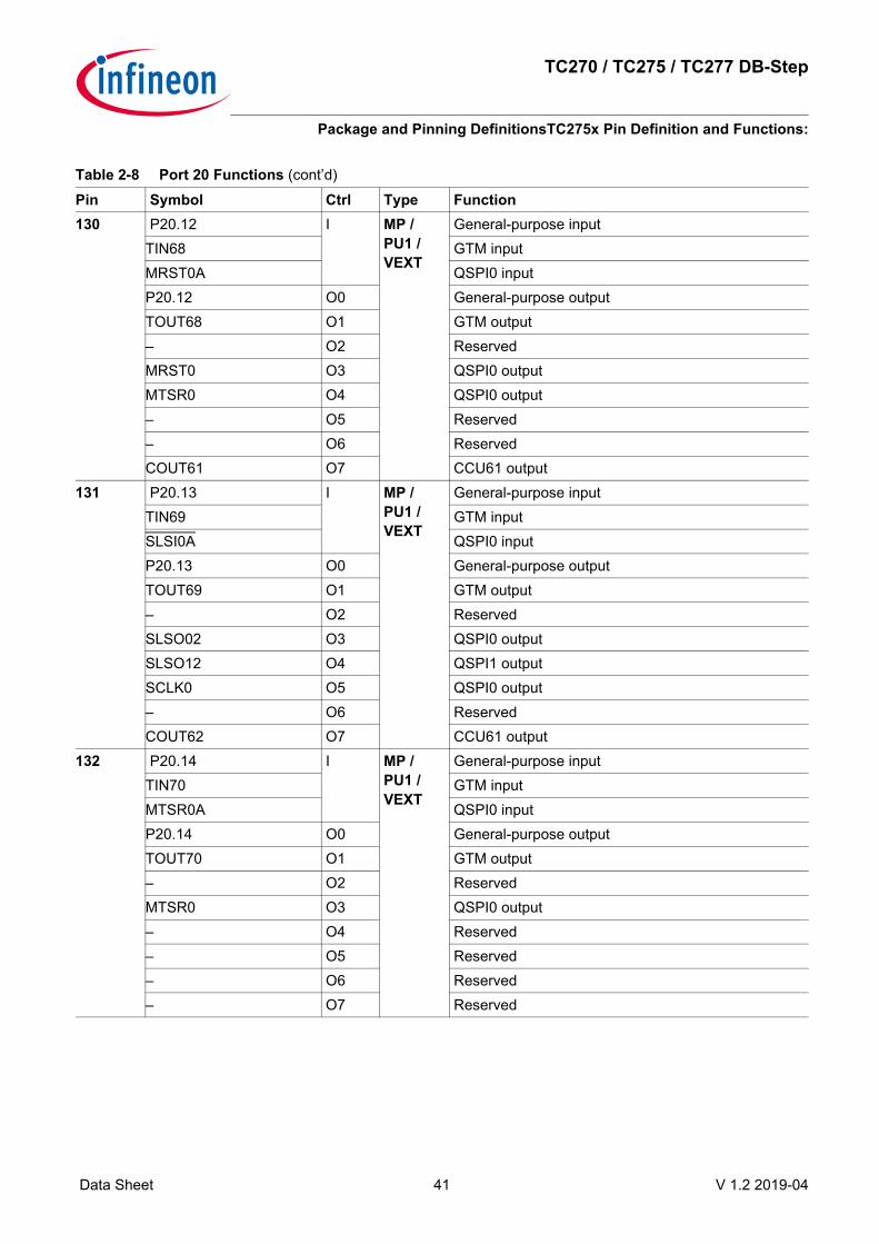
130 P20.12 I MP /PU1 /VEXT
General-purpose inputTIN68 GTM inputMRST0A QSPI0 inputP20.12 O0 General-purpose outputTOUT68 O1 GTM output– O2 ReservedMRST0 O3 QSPI0 outputMTSR0 O4 QSPI0 output– O5 Reserved– O6 ReservedCOUT61 O7 CCU61 output
131 P20.13 I MP /PU1 /VEXT
General-purpose inputTIN69 GTM inputSLSI0A QSPI0 inputP20.13 O0 General-purpose outputTOUT69 O1 GTM output– O2 ReservedSLSO02 O3 QSPI0 outputSLSO12 O4 QSPI1 outputSCLK0 O5 QSPI0 output– O6 ReservedCOUT62 O7 CCU61 output
132 P20.14 I MP /PU1 /VEXT
General-purpose inputTIN70 GTM inputMTSR0A QSPI0 inputP20.14 O0 General-purpose outputTOUT70 O1 GTM output– O2 ReservedMTSR0 O3 QSPI0 output– O4 Reserved– O5 Reserved– O6 Reserved– O7 Reserved
Table 2-8 Port 20 Functions (cont’d)Pin Symbol Ctrl Type Function

TC270 / TC275 / TC277 DB-Step
Package and Pinning DefinitionsTC275x Pin Definition and Functions:
Data Sheet 42 V 1.2 2019-04
Table 2-9 Port 21 FunctionsPin Symbol Ctrl Type Function105 P21.0 I A2 /
PU1 /VDDP3
General-purpose inputTIN51 GTM inputP21.0 O0 General-purpose outputTOUT51 O1 GTM output– O2 Reserved– O3 Reserved– O4 Reserved– O5 ReservedETHMDC O6 ETH output– O7 ReservedHSM1 HWOU
THSM output 1
106 P21.1 I A2 / PU1 /VDDP3
General-purpose inputTIN52 GTM inputETHMDIOB ETH input
(Not for production purposes)P21.1 O0 General-purpose outputTOUT52 O1 GTM output– O2 Reserved– O3 Reserved– O4 Reserved– O5 ReservedETHMDIO O6 ETH output
(Not for production purposes)– O7 ReservedHSM2 HWOU
THSM output 2

TC270 / TC275 / TC277 DB-Step
Package and Pinning DefinitionsTC275x Pin Definition and Functions:
Data Sheet 43 V 1.2 2019-04
107 P21.2 I LVDSH_N/ PU1 /VDDP3
General-purpose inputTIN53 GTM inputMRST2CN QSPI2 input (LVDS)MRST3FN QSPI3 input (LVDS)ARX3GN ASCLIN3 input (LVDS)EMGSTOPB SCU inputRXDN HSCT input (LVDS)P21.2 O0 General-purpose outputTOUT53 O1 GTM outputASLSO3 O2 ASCLIN3 output– O3 Reserved– O4 ReservedETHMDC O5 ETH output– O6 Reserved– O7 Reserved
108 P21.3 I LVDSH_P/ PU1 /VDDP3
General-purpose inputTIN54 GTM inputMRST2CP QSPI2 input (LVDS)MRST3FP QSPI3 input (LVDS)ARX3GP ASCLIN3 input (LVDS)RXDP HSCT input (LVDS)P21.3 O0 General-purpose outputTOUT54 O1 GTM output– O2 Reserved– O3 Reserved– O4 Reserved– O5 Reserved– O6 Reserved– O7 ReservedETHMDIOD HWOU
TETH input/output
Table 2-9 Port 21 Functions (cont’d)Pin Symbol Ctrl Type Function

TC270 / TC275 / TC277 DB-Step
Package and Pinning DefinitionsTC275x Pin Definition and Functions:
Data Sheet 44 V 1.2 2019-04
109 P21.4 I LVDSH_N/ PU1 /VDDP3
General-purpose inputTIN55 GTM inputP21.4 O0 General-purpose outputTOUT55 O1 GTM output– O2 Reserved– O3 Reserved– O4 Reserved– O5 Reserved– O6 Reserved– O7 ReservedTXDN HSCT HSCT output (LVDS)
110 P21.5 I LVDSH_P/ PU1 /VDDP3
General-purpose inputTIN56 GTM inputP21.5 O0 General-purpose outputTOUT56 O1 GTM outputASCLK3 O2 ASCLIN3 output– O3 Reserved– O4 Reserved– O5 Reserved– O6 Reserved– O7 ReservedTXDP HSCT HSCT output (LVDS)
1111) P21.6 I A2 / PU /VDDP3
General-purpose inputTIN57 GTM inputARX3F ASCLIN3 inputTGI2 OCDS inputTDI OCDS (JTAG) inputT5EUDA GPT120 inputP21.6 O0 General-purpose outputTOUT57 O1 GTM outputASLSO3 O2 ASCLIN3 output– O3 Reserved– O4 ReservedSYSCLK O5 HSCT output– O6 ReservedT3OUT O7 GPT120 outputTGO2 HWOU
TOCDS; ENx
Table 2-9 Port 21 Functions (cont’d)Pin Symbol Ctrl Type Function

TC270 / TC275 / TC277 DB-Step
Package and Pinning DefinitionsTC275x Pin Definition and Functions:
Data Sheet 45 V 1.2 2019-04
113 P21.7 I A2 / PU /VDDP3
General-purpose inputTIN58 GTM inputDAP2 OCDS inputTGI3 OCDS inputTDO OCDS (JTAG) input
The JTAG TDO function is overlayed with P21.7 via a double bond. In JTAG mode this pin is used as TDO, after power-on reset it is HighZ. In DAP mode this pin is used as P21.7 and controlled by the related port control logic
ETHRXERB ETH inputT5INA GPT120 inputP21.7 O0 General-purpose outputTOUT58 O1 GTM outputATX3 O2 ASCLIN3 outputASCLK3 O3 ASCLIN3 output– O4 Reserved– O5 Reserved– O6 ReservedT6OUT O7 GPT120 outputTGO3 HWOU
TOCDS; ENx
TDO OCDS (JTAG); ENxThe JTAG TDO function is overlayed with P21.7 via a double bond. In JTAG mode this pin is used as TDO, after power-on reset it is HighZ. In DAP mode this pin is used as P21.7 and controlled by the related port control logic
1) For an Emulation Device in a non Fusion Quad package this pin is used as VDDPSB (3.3V)
Table 2-9 Port 21 Functions (cont’d)Pin Symbol Ctrl Type Function

TC270 / TC275 / TC277 DB-Step
Package and Pinning DefinitionsTC275x Pin Definition and Functions:
Data Sheet 46 V 1.2 2019-04
Table 2-10 Port 22 FunctionsPin Symbol Ctrl Type Function95 P22.0 I LVDSM_N /
PU1 / VEXT
General-purpose inputTIN47 GTM inputMTSR3E QSPI3 inputP22.0 O0 General-purpose outputTOUT47 O1 GTM outputATX3N O2 ASCLIN3 output (LVDS)MTSR3 O3 QSPI3 outputSCLK3N O4 QSPI3 output (LVDS)FCLN1 O5 MSC1 output (LVDS)FCLND1 O6 MSC1 output (LVDS)– O7 Reserved
96 P22.1 I LVDSM_P /PU1 / VEXT
General-purpose inputTIN48 GTM inputMRST3E QSPI3 inputP22.1 O0 General-purpose outputTOUT48 O1 GTM outputATX3P O2 ASCLIN3 output (LVDS)MRST3 O3 QSPI3 outputSCLK3P O4 QSPI3 output (LVDS)FCLP1 O5 MSC1 output (LVDS)– O6 Reserved– O7 Reserved
97 P22.2 I LVDSM_N /PU1 / VEXT
General-purpose inputTIN49 GTM inputSLSI3D QSPI3 inputP22.2 O0 General-purpose outputTOUT49 O1 GTM output– O2 ReservedSLSO312 O3 QSPI3 outputMTSR3N O4 QSPI3 output (LVDS)SON1 O5 MSC1 output (LVDS)SOND1 O6 MSC1 output (LVDS)– O7 Reserved

TC270 / TC275 / TC277 DB-Step
Package and Pinning DefinitionsTC275x Pin Definition and Functions:
Data Sheet 47 V 1.2 2019-04
98 P22.3 I LVDSM_P /PU1 / VEXT
General-purpose inputTIN50 GTM inputSCLK3E QSPI3 inputP22.3 O0 General-purpose outputTOUT50 O1 GTM output– O2 ReservedSCLK3 O3 QSPI3 outputMTSR3P O4 QSPI3 output (LVDS)SOP1 O5 MSC1 output (LVDS)– O6 Reserved– O7 Reserved
Table 2-11 Port 23 FunctionsPin Symbol Ctrl Type Function89 P23.0 I LP /
PU1 /VEXT
General-purpose inputTIN41 GTM inputP23.0 O0 General-purpose outputTOUT41 O1 GTM output– O2 Reserved– O3 Reserved– O4 Reserved– O5 Reserved– O6 Reserved– O7 Reserved
90 P23.1 I MP+ /PU1 /VEXT
General-purpose inputTIN42 GTM inputSDI10 MSC1 inputP23.1 O0 General-purpose outputTOUT42 O1 GTM outputARTS1 O2 ASCLIN1 outputSLSO313 O3 QSPI3 outputGTMCLK0 O4 GTM output– O5 ReservedEXTCLK0 O6 SCU output– O7 Reserved
Table 2-10 Port 22 Functions (cont’d)Pin Symbol Ctrl Type Function
TC270 / TC275 / TC277 DB-Step
Package and Pinning DefinitionsTC275x Pin Definition and Functions:
Data Sheet 48 V 1.2 2019-04
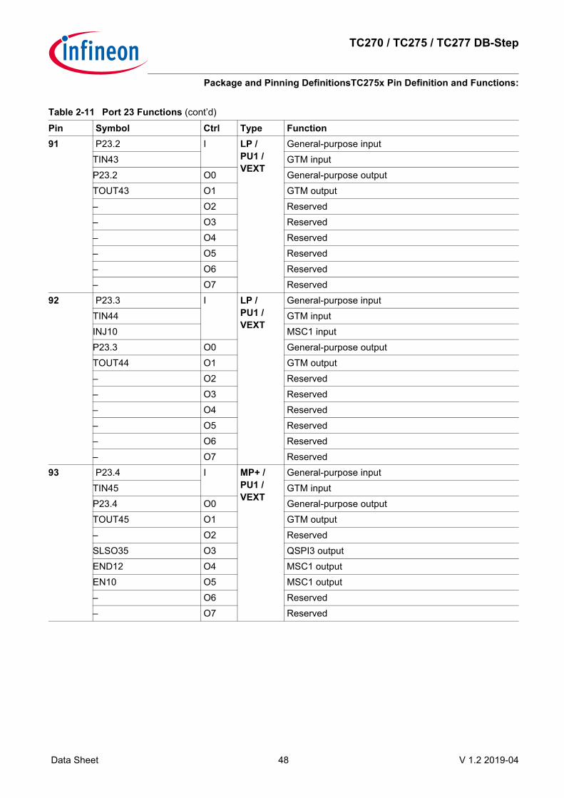
91 P23.2 I LP /PU1 /VEXT
General-purpose inputTIN43 GTM inputP23.2 O0 General-purpose outputTOUT43 O1 GTM output– O2 Reserved– O3 Reserved– O4 Reserved– O5 Reserved– O6 Reserved– O7 Reserved
92 P23.3 I LP /PU1 /VEXT
General-purpose inputTIN44 GTM inputINJ10 MSC1 inputP23.3 O0 General-purpose outputTOUT44 O1 GTM output– O2 Reserved– O3 Reserved– O4 Reserved– O5 Reserved– O6 Reserved– O7 Reserved
93 P23.4 I MP+ /PU1 /VEXT
General-purpose inputTIN45 GTM inputP23.4 O0 General-purpose outputTOUT45 O1 GTM output– O2 ReservedSLSO35 O3 QSPI3 outputEND12 O4 MSC1 outputEN10 O5 MSC1 output– O6 Reserved– O7 Reserved
Table 2-11 Port 23 Functions (cont’d)Pin Symbol Ctrl Type Function

TC270 / TC275 / TC277 DB-Step
Package and Pinning DefinitionsTC275x Pin Definition and Functions:
Data Sheet 49 V 1.2 2019-04
94 P23.5 I MP+ /PU1 /VEXT
General-purpose inputTIN46 GTM inputP23.5 O0 General-purpose outputTOUT46 O1 GTM output– O2 ReservedSLSO34 O3 QSPI3 outputEND13 O4 MSC1 outputEN11 O5 MSC1 output– O6 Reserved– O7 Reserved
Table 2-12 Port 32 FunctionsPin Symbol Ctrl Type Function84 P32.0 I LP /
EVR13 SMPS -> PD, GPIO - > PU/VEXT
General-purpose inputTIN36 GTM inputFDEST PMU inputVGATE1N SMPS mode: analog output. External Pass Device
gate control for EVR13P32.0 O0 General-purpose outputTOUT36 O1 GTM output– O2 Reserved– O3 Reserved– O4 Reserved– O5 Reserved– O6 Reserved– O7 Reserved
86 P32.2 I LP / PU1 /VEXT
General-purpose inputTIN38 GTM inputARX3D ASCLIN3 inputRXDCAN3B CAN node 3 inputP32.2 O0 General-purpose outputTOUT38 O1 GTM outputATX3 O2 ASCLIN3 output– O3 Reserved– O4 Reserved– O5 ReservedDCDCSYNC O6 SCU output– O7 Reserved
Table 2-11 Port 23 Functions (cont’d)Pin Symbol Ctrl Type Function

TC270 / TC275 / TC277 DB-Step
Package and Pinning DefinitionsTC275x Pin Definition and Functions:
Data Sheet 50 V 1.2 2019-04
87 P32.3 I LP / PU1 /VEXT
General-purpose inputTIN39 GTM inputP32.3 O0 General-purpose outputTOUT39 O1 GTM outputATX3 O2 ASCLIN3 output– O3 ReservedASCLK3 O4 ASCLIN3 outputTXDCAN3 O5 CAN node 3 output– O6 Reserved– O7 Reserved
88 P32.4 I MP+ / PU1 /VEXT
General-purpose inputTIN40 GTM inputACTS1B ASCLIN1 inputSDI12 MSC1 inputP32.4 O0 General-purpose outputTOUT40 O1 GTM output– O2 ReservedEND12 O3 MSC1 outputGTMCLK1 O4 GTM outputEN10 O5 MSC1 outputEXTCLK1 O6 SCU outputCOUT63 O7 CCU60 output
Table 2-13 Port 33 FunctionsPin Symbol Ctrl Type Function70 P33.0 I LP /
PU1 /VEXT
General-purpose inputTIN22 GTM inputDSITR0E DSADC channel 0 input EP33.0 O0 General-purpose outputTOUT22 O1 GTM output– O2 Reserved– O3 Reserved– O4 Reserved– O5 ReservedVADCG2BFL0 O6 VADC output– O7 Reserved
Table 2-12 Port 32 Functions (cont’d)Pin Symbol Ctrl Type Function

TC270 / TC275 / TC277 DB-Step
Package and Pinning DefinitionsTC275x Pin Definition and Functions:
Data Sheet 51 V 1.2 2019-04
71 P33.1 I LP /PU1 /VEXT
General-purpose inputTIN23 GTM inputPSIRX0C PSI5 inputSENT9C SENT inputDSCIN2B DSADC channel 2 input BDSITR1E DSADC channel 1 input EP33.1 O0 General-purpose outputTOUT23 O1 GTM outputASLSO3 O2 ASCLIN3 output– O3 ReservedDSCOUT2 O4 DSADC channel 2 outputVADCEMUX02 O5 VADC outputVADCG2BFL1 O6 VADC output– O7 Reserved
72 P33.2 I LP /PU1 /VEXT
General-purpose inputTIN24 GTM inputSENT8C SENT inputDSDIN2B DSADC channel 2 input BDSITR2E DSADC channel 2 input EP33.2 O0 General-purpose outputTOUT24 O1 GTM outputASCLK3 O2 ASCLIN3 output– O3 ReservedPSITX0 O4 PSI5 outputVADCEMUX01 O5 VADC outputVADCG2BFL2 O6 VADC output– O7 Reserved
Table 2-13 Port 33 Functions (cont’d)Pin Symbol Ctrl Type Function

TC270 / TC275 / TC277 DB-Step
Package and Pinning DefinitionsTC275x Pin Definition and Functions:
Data Sheet 52 V 1.2 2019-04
73 P33.3 I LP /PU1 /VEXT
General-purpose inputTIN25 GTM inputPSIRX1C PSI5 inputSENT7C SENT inputDSCIN1B DSADC channel 1 input BP33.3 O0 General-purpose outputTOUT25 O1 GTM output– O2 Reserved– O3 ReservedDSCOUT1 O4 DSADC channel 1 outputVADCEMUX00 O5 VADC outputVADCG2BFL3 O6 VADC output– O7 Reserved
74 P33.4 I LP /PU1 /VEXT
General-purpose inputTIN26 GTM inputSENT6C SENT inputCTRAPC CCU61 inputDSDIN1B DSADC channel 1 input BDSITR0F DSADC channel 0 input FP33.4 O0 General-purpose outputTOUT26 O1 GTM outputARTS2 O2 ASCLIN2 output– O3 ReservedPSITX1 O4 PSI5 outputVADCEMUX12 O5 VADC outputVADCG0BFL0 O6 VADC output– O7 Reserved
Table 2-13 Port 33 Functions (cont’d)Pin Symbol Ctrl Type Function

TC270 / TC275 / TC277 DB-Step
Package and Pinning DefinitionsTC275x Pin Definition and Functions:
Data Sheet 53 V 1.2 2019-04
75 P33.5 I LP /PU1 /VEXT
General-purpose inputTIN27 GTM inputACTS2B ASCLIN2 inputPSIRX2C PSI5 inputPSISRXC PSI5-S inputSENT5C SENT inputCCPOS2C CCU61 inputT4EUDB GPT120 inputDSCIN0B DSADC channel 0 input BDSITR1F DSADC channel 1 input FP33.5 O0 General-purpose outputTOUT27 O1 GTM outputSLSO07 O2 QSPI0 outputSLSO17 O3 QSPI1 outputDSCOUT0 O4 DSADC channel 0 outputVADCEMUX11 O5 VADC outputVADCG0BFL1 O6 VADC output– O7 Reserved
76 P33.6 I LP /PU1 /VEXT
General-purpose inputTIN28 GTM inputSENT4C SENT inputCCPOS1C CCU61 inputT2EUDB GPT120 inputDSDIN0B DSADC channel 0 input BDSITR2F DSADC channel 2 input FP33.6 O0 General-purpose outputTOUT28 O1 GTM outputASLSO2 O2 ASCLIN2 output- O3 ReservedPSITX2 O4 PSI5 outputVADCEMUX10 O5 VADC outputVADCG1BFL0 O6 VADC outputPSISTX O7 PSI5-S output
Table 2-13 Port 33 Functions (cont’d)Pin Symbol Ctrl Type Function

TC270 / TC275 / TC277 DB-Step
Package and Pinning DefinitionsTC275x Pin Definition and Functions:
Data Sheet 54 V 1.2 2019-04
77 P33.7 I LP /PU1 /VEXT
General-purpose inputTIN29 GTM inputRXDCAN0E CAN node 0 inputREQ8 SCU inputCCPOS0C CCU61 inputT2INB GPT120 inputP33.7 O0 General-purpose outputTOUT29 O1 GTM outputASCLK2 O2 ASCLIN2 outputSLSO37 O3 QSPI3 output– O4 Reserved– O5 ReservedVADCG1BFL1 O6 VADC output– O7 Reserved
78 P33.8 I MP /HighZ/VEXT
General-purpose inputTIN30 GTM inputARX2E ASCLIN2 inputEMGSTOPA SCU inputP33.8 O0 General-purpose outputTOUT30 O1 GTM outputATX2 O2 ASCLIN2 outputSLSO32 O3 QSPI3 output– O4 ReservedTXDCAN0 O5 CAN node 0 output– O6 ReservedCOUT62 O7 CCU61 outputSMUFSP HWOU
TSMU
79 P33.9 I LP /PU1 /VEXT
General-purpose inputTIN31 GTM inputP33.9 O0 General-purpose outputTOUT31 O1 GTM outputATX2 O2 ASCLIN2 outputSLSO31 O3 QSPI3 outputASCLK2 O4 ASCLIN2 output– O5 Reserved– O6 ReservedCC62 O7 CCU61 output
Table 2-13 Port 33 Functions (cont’d)Pin Symbol Ctrl Type Function

TC270 / TC275 / TC277 DB-Step
Package and Pinning DefinitionsTC275x Pin Definition and Functions:
Data Sheet 55 V 1.2 2019-04
80 P33.10 I MP /PU1 /VEXT
General-purpose inputTIN32 GTM inputSLSI3C QSPI3 inputP33.10 O0 General-purpose outputTOUT32 O1 GTM outputSLSO16 O2 QSPI1 outputSLSO311 O3 QSPI3 outputASLSO1 O4 ASCLIN1 outputPSISCLK O5 PSI5-S output– O6 ReservedCOUT61 O7 CCU61 output
81 P33.11 I MP /PU1 /VEXT
General-purpose inputTIN33 GTM inputSCLK3D QSPI3 inputP33.11 O0 General-purpose outputTOUT33 O1 GTM outputASCLK1 O2 ASCLIN1 outputSCLK3 O3 QSPI3 output– O4 Reserved– O5 ReservedDSCGPWMN O6 DSADC outputCC61 O7 CCU61 output
82 P33.12 I MP /PU1 /VEXT
General-purpose inputTIN34 GTM inputMTSR3D QSPI3 inputP33.12 O0 General-purpose outputTOUT34 O1 GTM outputATX1 O2 ASCLIN1 outputMTSR3 O3 QSPI3 outputASCLK1 O4 ASCLIN1 output– O5 ReservedDSCGPWMP O6 DSADC outputCOUT60 O7 CCU61 output
Table 2-13 Port 33 Functions (cont’d)Pin Symbol Ctrl Type Function

TC270 / TC275 / TC277 DB-Step
Package and Pinning DefinitionsTC275x Pin Definition and Functions:
Data Sheet 56 V 1.2 2019-04
83 P33.13 I MP /PU1 /VEXT
General-purpose inputTIN35 GTM inputARX1F ASCLIN1 inputMRST3D QSPI3 inputDSSGNB DSADC inputINJ11 MSC1 inputP33.13 O0 General-purpose outputTOUT35 O1 GTM outputATX1 O2 ASCLIN1 outputMRST3 O3 QSPI3 outputSLSO26 O4 QSPI2 output– O5 ReservedDCDCSYNC O6 SCU outputCC60 O7 CCU61 output
Table 2-14 Port 40 FunctionsPin Symbol Ctrl Type Function44 P40.0 I S /
HighZ /VDDM
General-purpose inputVADCG3.0 VADC analog input channel 0 of group 3DS2PB DSADC: positive analog input channe of DSADC 2, pin
BCCPOS0D CCU60 inputSENT0A SENT input
43 P40.1 I S /HighZ /VDDM
General-purpose inpu.tVADCG3.1 VADC analog input channel 1 of group 3 (MD)DS2NB DSADC: negative analog of input channel 2, pin BCCPOS1B CCU60 inputSENT1A SENT input
42 P40.2 I S /HighZ /VDDM
General-purpose inpu.tVADCG3.2 VADC analog input channel 2 of group 3 (MD)CCPOS1D CCU60 inputSENT2A SENT input
41 P40.3 I S /HighZ /VDDM
General-purpose inputVADCG3.3 VADC analog input channel 3 of group 3CCPOS2B CCU60 inputSENT3A SENT input
Table 2-13 Port 33 Functions (cont’d)Pin Symbol Ctrl Type Function

TC270 / TC275 / TC277 DB-Step
Package and Pinning DefinitionsTC275x Pin Definition and Functions:
Data Sheet 57 V 1.2 2019-04
38 P40.4 I S /HighZ /VDDM
General-purpose inputVADCG4.0 VADC analog input channel 0 of group 4CCPOS2D CCU60 inputSENT4A SENT input
37 P40.5 I S /HighZ /VDDM
General-purpose inputVADCG4.1 VADC analog input channel 1 of group 4 (MD)CCPOS0D CCU61 inputSENT5A SENT input
35 P40.6 I S /HighZ /VDDM
General-purpose inputVADCG4.4 VADC analog input channel 4 of group 4DS3PA DSADC: positive analog input of channel 3, pin ACCPOS1B CCU61 inputSENT6A SENT input
34 P40.7 I S /HighZ /VDDM
General-purpose inputVADCG4.5 VADC analog input channel 5 of group 4DS3NA DSADC: negative analog input of channel 3, pin ACCPOS1D CCU61 inputSENT7A SENT input
33 P40.8 I S /HighZ /VDDM
General-purpose inputVADCG4.6 VADC analog input channel 6 of group 4DS3PB DSADC: positive analog input of channel 3, pin BCCPOS2B CCU61 inputSENT8A SENT input
32 P40.9 I S /HighZ /VDDM
General-purpose inputVADCG4.7 VADC analog input channel 7 of group 4DS3NB DSADC: negative analog input of channel 3, pin BCCPOS2D CCU61 inputSENT9A SENT input
Table 2-15 Analog InputsPin Symbol Ctrl Type Function67 AN0 I D /
HighZ /VDDM
Analog input 0VADCG0.0 VADC analog input channel 0 of group 0DS1PA DSADC: positive analog of input channel 1, pin A
66 AN1 I D /HighZ /VDDM
Analog input 1VADCG0.1 VADC analog input channel 1 of group 0 (MD)DS1NA DSADC: negative analog input of channel 1, pin A
Table 2-14 Port 40 Functions (cont’d)Pin Symbol Ctrl Type Function

TC270 / TC275 / TC277 DB-Step
Package and Pinning DefinitionsTC275x Pin Definition and Functions:
Data Sheet 58 V 1.2 2019-04
65 AN2 I D /HighZ /VDDM
Analog input 2VADCG0.2 VADC analog input channel 2 of group 0 (MD)DS0PA DSADC: positive analog input of channel 0, pin A
64 AN3 I D /HighZ /VDDM
Analog input 3VADCG0.3 VADC analog input channel 3 of group 0DS0NA DSADC: negative analog input of channel 0, pin A
63 AN4 I D /HighZ /VDDM
Analog input 4VADCG0.4 VADC analog input channel 4 of group 0
62 AN5 I D /HighZ /VDDM
Analog input 5VADCG0.5 VADC analog input channel 5 of group 0
61 AN6 I D /HighZ /VDDM
Analog input 6VADCG0.6 VADC analog input channel 6 of group 0
60 AN7 I D /HighZ /VDDM
Analog input 7VADCG0.7 VADC analog input channel 7 of group 0 (with pull
down diagnostics)59 AN8 I D /
HighZ /VDDM
Analog input 8VADCG1.0 VADC analog input channel 0 of group 1
58 AN10 I D /HighZ /VDDM
Analog input 10VADCG1.2 VADC analog input channel 2 of group 1 (MD)
57 AN11 I D /HighZ /VDDM
Analog input 11VADCG1.3 VADC analog input channel 3 of group 1 (with pull
down diagnostics)56 AN12 I D /
HighZ /VDDM
Analog input 12VADCG1.4 VADC analog input channel 4 of group 1
55 AN13 I D /HighZ /VDDM
Analog input 13VADCG1.5 VADC analog input channel 5 of group 1
50 AN16 I D /HighZ /VDDM
Analog input 16VADCG2.0 VADC analog input channel 0 of group 2
49 AN17 I D /HighZ /VDDM
Analog input 17VADCG2.1 VADC analog input channel 1 of group 2 (MD)
48 AN18 I D /HighZ /VDDM
Analog input 18VADCG2.2 VADC analog input channel 2 of group 2 (MD)
Table 2-15 Analog Inputs (cont’d)Pin Symbol Ctrl Type Function

TC270 / TC275 / TC277 DB-Step
Package and Pinning DefinitionsTC275x Pin Definition and Functions:
Data Sheet 59 V 1.2 2019-04
47 AN19 I D /HighZ /VDDM
Analog input 19VADCG2.3 VADC analog input channel 3 of group 2 (with pull
down diagnostics)46 AN20 I D /
HighZ /VDDM
Analog input 20VADCG2.4 I VADC analog input channel 4 of group 2DS2PA I DSADC: positive analog input of channel 2, pin A
45 AN21 I D /HighZ /VDDM
Analog input 21VADCG2.5 I VADC analog input channel 5 of group 2DS2NA I DSADC: negative analog input of channel
of DSADC 2, pin A44 AN24 I S /
HighZ /VDDM
Analog input 24VADCG3.0 VADC analog input channel 0 of group 3DS2PB DSADC: positive analog input of channel 2, pin BSENT0A SENT input channel 0, pin A
43 AN25 I S /HighZ /VDDM
Analog input 24VADCG3.1 VADC analog input channel 1 of group 3 (MD)DS2NB DSADC: negative analog input of channel 2, pin BSENT1A SENT input channel 1, pin A
42 AN26 I S /HighZ /VDDM
Analog input 26VADCG3.2 VADC analog input channel 2 of group 3 (MD)SENT2A SENT input channel 2, pin A
41 AN27 I S /HighZ /VDDM
Analog input 27VADCG3.3 VADC analog input channel 3 of group 3 (with pull
down diagnostics)SENT3A SENT input channel 3, pin A
40 AN28 I D /HighZ /VDDM
Analog input 28VADCG3.4 VADC analog input channel 4 of group 3
39 AN29 I D /HighZ /VDDM
Analog input 29VADCG3.5 VADC analog input channel 5 of group 3
38 AN32 I S /HighZ /VDDM
Analog input 32VADCG4.0 VADC analog input channel 0 of group 4SENT4A SENT input channel 4, pin A
37 AN33 I S /HighZ /VDDM
Analog input 33VADCG4.1 VADC analog input channel 1 of group 4 (MD)SENT5A SENT input channel 5, pin A
36 AN35 I D /HighZ /VDDM
Analog input 35VADCG4.3 VADC analog input channel 3 of group 4 (with pull
down diagnostics)
Table 2-15 Analog Inputs (cont’d)Pin Symbol Ctrl Type Function

TC270 / TC275 / TC277 DB-Step
Package and Pinning DefinitionsTC275x Pin Definition and Functions:
Data Sheet 60 V 1.2 2019-04
35 AN36 I S /HighZ /VDDM
Analog input 34VADCG4.4 VADC analog input channel 4 of group 4DS3PA DSADC: positive analog input of channel
of DSADC 3, pin ASENT6A SENT input channel 6, pin A
34 AN37 I S /HighZ /VDDM
Analog input 37VADCG4.5 VADC analog input channel 5 of group 4DS3NA DSADC: negative analog input of channel
of DSADC 3, pin ASENT7A SENT input channel 7, pin A
33 AN38 I S /HighZ /VDDM
Analog input 38VADCG4.6 VADC analog input channel 6 of group 4DS3PB DSADC: positive analog input of channel
of DSADC 3, pin BSENT8A SENT input channel 8, pin A
32 AN39 I S /HighZ /VDDM
Analog input 39VADCG4.7 VADC analog input channel 7 of group 4DS3NB DSADC: negative analog input of channel
of DSADC 3, pin BSENT9A SENT input channel 9, pin A
31 AN44 I D /HighZ /VDDM
Analog input 44VADCG5.4 VADC analog input channel 4 of group 5DS3PC DSADC: positive analog input of channel
of DSADC 3, pin C30 AN45 I D /
HighZ /VDDM
Analog input 45VADCG5.5 VADC analog input channel 5 of group 5DS3NC DSADC: negative analog input of channel
of DSADC 3, pin C29 AN46 I D /
HighZ /VDDM
Analog input 46VADCG5.6 VADC analog input channel 6 of group 5DS3PD DSADC: positive analog input of channel
of DSADC 3, pin D28 AN47 I D /
HighZ /VDDM
Analog input 47VADCG5.7 VADC analog input channel 7 of group 5DS3ND DSADC: negative analog input of channel
of DSADC 3, pin D
Table 2-15 Analog Inputs (cont’d)Pin Symbol Ctrl Type Function

TC270 / TC275 / TC277 DB-Step
Package and Pinning DefinitionsTC275x Pin Definition and Functions:
Data Sheet 61 V 1.2 2019-04
Table 2-16 System I/OPin Symbol Ctrl Type Function121 PORST I I /
PD /VEXT
Power On Reset InputAdditional strong PD in case of power fail.
122 ESR0 I/O MP /OD /VEXT
External System Request Reset 0Default configuration during and after reset is open-drain driver. The driver drives low during power-on reset. This is valid additionally after deactivation of PORST until the internal reset phase has finished. See also SCU chapter for details.Default after power-on can be different. See also SCU chapter ´Reset Control Unit´ and SCU_IOCR register description.
EVRWUP I EVR Wakeup Pin120 ESR1 I/O MP / PU1 /
VEXTExternal System Request Reset 1Default NMI function. See also SCU chapter ´Reset Control Unit´ and SCU_IOCR register description.
EVRWUP I EVR Wakeup Pin85 VGATE1P O VGATE1P
/- /VEXT
External Pass Device gate control for EVR13
112 TMS I A2 / PD /VDDP3
JTAG Module State Machine Control InputDAP1 I/O Device Access Port Line 1
114 TRST I A2 / PD /VDDP3
JTAG Module Reset/Enable Input
115 TCK I A2 / PD /VDDP3
JTAG Module Clock InputDAP0 I Device Access Port Line 0
102 XTAL1 I XTAL1 /- /VDDP3
Main Oscillator/PLL/Clock Generator Input
103 XTAL2 O XTAL2 /- /VDDP3
Main Oscillator/PLL/Clock Generator Output
Table 2-17 SupplyPin Symbol Ctrl Type Function52 VAREF1 I Vx Positive Analog Reference Voltage 1
51 VAGND1 I Vx Negative Analog Reference Voltage 1

TC270 / TC275 / TC277 DB-Step
Package and Pinning DefinitionsTC275x Pin Definition and Functions:
Data Sheet 62 V 1.2 2019-04
Legend:Column “Ctrl.”:I = Input (for GPIO port Lines with IOCR bit field Selection PCx = 0XXXB)O = OutputO0 = Output with IOCR bit field selection PCx = 1X000BO1 = Output with IOCR bit field selection PCx = 1X001B (ALT1)O2 = Output with IOCR bit field selection PCx = 1X010B (ALT2)
26 VAREF2 I Vx Positive Analog Reference Voltage 2
27 VAGND2 I Vx Negative Analog Reference Voltage 2
54 VDDM I Vx ADC Analog Power Supply (3.3V / 5V)
101 VSS I Vx Digital Ground
10 VDD / VDDSB I Vx Emulation Device: Emulation SRAM Standby Power Supply (1.3V) (Emulation Device only).Production Device: VDD (1.3V).
123, 68, 24
VDD I Vx Digital Core Power Supply (1.3V)
100 VDD I Vx Digital Core Power Supply (1.3V).The supply pin inturn supplies the main XTAL Oscillator/PLL (1.3V) . A higher decoupling capacitor is therefore recommended to the VSS pin for better noise immunity.
153, 99, 69, 25
VEXT I Vx External Power Supply (5V / 3.3V)
154 VDDP3 I Vx Digital Power Supply for Flash (3.3V).Can be also used as external 3.3V Power Supply for VFLEX.
104 VDDP3 I Vx Digital Power Supply for Oscillator, LVDSH and A2 pads (3.3V).The supply pin inturn supplies the main XTAL Oscillator/PLL (3.3V) . A higher decoupling capacitor is therefore recommended to the VSS pin for better noise immunity.
155 VDDFL3 I Vx Flash Power Supply (3.3V)
164 VFLEX I Vx Digital Power Supply for Flex Port Pads(5V / 3.3V)
53 VSSM I Vx Analog Ground for VDDM
Table 2-17 Supply (cont’d)Pin Symbol Ctrl Type Function

TC270 / TC275 / TC277 DB-Step
Package and Pinning DefinitionsTC275x Pin Definition and Functions:
Data Sheet 63 V 1.2 2019-04
O3 = Output with IOCR bit field selection PCx = 1X011B (ALT3)O4 = Output with IOCR bit field selection PCx = 1X100B (ALT4)O5 = Output with IOCR bit field selection PCx = 1X101B (ALT5)O6 = Output with IOCR bit field selection PCx = 1X110B (ALT6)O7 = Output with IOCR bit field selection PCx = 1X111B (ALT7)Column “Type”:LP = Pad class LP (5V/3.3V, LVTTL)MP = Pad class MP (5V/3.3V, LVTTL)MP+ = Pad class MP+ (5V/3.3V, LVTTL)MPR = Pad class MPR (5V/3.3V, LVTTL)A2 = Pad class A2 (3.3V, LVTTL)LVDSM = Pad class LVDSM (LVDS/CMOS 5V/3.3V)LVDSH = Pad class LVDSH (LVDS/CMOS 3.3V)S = Pad class S (ADC overlayed with General Purpose Input)D = Pad class D (ADC)PU = with pull-up device connected during reset (PORST = 0)PU1 = with pull-up device connected during reset (PORST = 0)1) 2) 3)
PD = with pull-down device connected during reset (PORST = 0)PD1 = with pull-down device connected during reset (PORST = 0)1) 2) 3) PX = Behavior depends on usage: PD in EVR13 SMPS Mode and PU1 in GPIO ModeOD = open drain during reset (PORST = 0)HighZ = tri-state during reset (PORST = 0)PORST = PORST input padXTAL1 = XTAL1 input padXTAL2 = XTAL2 input padVGATE1P = VGATE1PVGATE3P = VGATE3PVx = Supply (the Exposed Pad is also considered as VSS and shall be connected to ground)NC = These pins are reserved for future extensions and shall not be connected externallyNC1 = These pins are not connected on package level and will not be used for future extensionsNCVDDPSB = This pin has a different functionality in an Production Device and an Emulation Device. For detailspls. see Pin/Ball description of this pin.NCVDDSB = This pin has a different functionality in an Production Device and an Emulation Device. For detailspls. see Pin/Ball description of this pin.
2.1.2 Emergency Stop FunctionThe Emergency Stop function can be used to force GPIOs (General Purpose Inputs/Outputs) via an external inputsignal (EMGSTOPA or EMGSTOPB) into a defined state:• Input state and• PU or High-Z depending on HWCFG[6] level latched during PORST activeControl of the Emergency Stop function:
1) The default state of GPIOs (Px.y) during and after PORST active is controllled via HWCFG[6] (P14.4). HWCFG[6] has a weak internal pull-up active at start-up if the pin is left unconnected.See also User´s Manual, “Introduction Chapter”, “General Purpose I/O Ports and Peripheral I/O Lines”, Figure: “Default state of port pins during and after reset”.
2) If HWCFG[6] is left unconnected or is externally pulled high, weak internal pull-ups (PU1) / pull-downs (PD1) are active during and after reset.
3) If HWCFG[6] is connected to ground, the PD1 / PU1 pins are predominantly in HighZ during and after reset.

TC270 / TC275 / TC277 DB-Step
Package and Pinning DefinitionsTC275x Pin Definition and Functions:
Data Sheet 64 V 1.2 2019-04
• The Emergency Stop function can be enabled/disabled in the SCU (see chapter “SCU”, “Emergency Stop Control”)
• The Emergency Stop input signal, EMGSTOPA (P33.8) / EMGSTOPB (P21.2) , can selected in the SCU (see chapter “SCU”, “Emergency Stop Control”)
• On port level, each GPIO can be enabled/disabled for the Emergency Stop function via the Px_ESR (Port x Emergency Stop) registers in the port control logic (see chapter “General Purpose I/O Ports and Peripheral I/O Lines”, “Emergency Stop Register”).
The Emergency Stop function is available for all GPIO Ports with the following exceptions:• Not available for P20.2 (General Purpose Input/GPI only, overlayed with Testmode)• Not available for P40.x (analoge input ANx overlayed with GPI)• Not available for P32.0 EVR13 SMPS mode.• Not available for dedicated I/O without General Purpose Output function (e.g ESRx, TMS, TCK)The Emergency Stop function can be overruled on the following GPIO Ports:• P00.x: Emergency Stop can be overruled by the VADC. Overruling can be disabled via the control register
P00_SCR (see chapter “General Purpose I/O Ports and Peripheral I/O Lines”, P00)• P14.0 and P14.1: Emergency Stop can be overruled in the DXCPL mode (DAP over can physical layer mode).
No Overruling in the DXCM (Debug over can message) mode• P21.6: Emergency Stop can be overruled in JTAG mode if this pin is used as TDI• P21.7: Emergency Stop can be overruled in JTAG or Three Pin DAP mode• P20.0: Emergency Stop can be overruled in JTAG mode if this GPIO is used as TDI
2.1.3 Pull-Up/Pull-Down Reset Behavior of the Pins
In case of leakage test (PORST = 0 and TESTMODE = 0), the pull-down of the TRST pin is switched off. In caseof an user application (TESTMODE = 1), the pull-down of the TRST is always switched on.
Table 2-18 List of Pull-Up/Pull-Down Reset Behavior of the PinsPins PORST = 0 PORST = 1all GPIOs Pull-up if HWCFG[6] = 1 or High-Z if HWCFG[6] = 0TDI, TESTMODE Pull-upPORST1)
1) Pull-down with IPORST relevant is always activated when a primary supply monitor detects a violation.
Pull-down with IPORST relevant Pull-down with IPDLI relevantTRST, TCK, TMS Pull-downESR0 The open-drain driver is used to
drive low.2)
2)Valid additionally after deactivation of PORST until the internal reset phase has finished. See the SCU chapter for details.
Pull-up3)
3) See the SCU_IOCR register description.
ESR1 Pull-up3)
TDO Pull-up High-Z/Pull-up4)
4) Depends on JTAG/DAP selection with TRST.

TC270 / TC275 / TC277 DB-Step
Package and Pinning DefinitionsTC277x Pin Definition and Functions:
Data Sheet 65 V 1.2 2019-04
2.2 TC277x Pin Definition and Functions: BGA292Figure 2-2 is showing the TC277x Logic Symbol for the package variant: BGA292.
Figure 2-2 TC277x Logic Symbol for the package variant BGA292.
20 19 18 17 16 15 14 13 12 11 10 9 8 7 6 5 4 3 2 1
Y VSS P32.3 P32.2 P32.0 P33.13 P33.11 P33.9 P33.7 P33.5 P33.3 P33.1 AN5 AN10 VAGND1 VAREF1 VDDM VSSM AN20 AN21 NC Y
W VEXT VSS P32.4 VGATE1P P33.12 P33.10 P33.8 P33.6 P33.4 P33.2 P33.0 AN2 AN8 AN11 AN13 AN16 AN18 AN19 AN24 AN25 W
V P23.0 VEXT17 16 15 14 13 12 11 10 9 8 7 6 5 4
AN26 AN27 V
U P23.2 P23.1 U VSS P32.7 P32.6 P33.15 P34.5 P34.3 P34.1 AN1 AN3 AN7 AN9 AN14 AN17 NC U AN28 AN29 U
T P23.4 P23.3 T P23.5 VSS P32.5 P33.14 P34.4 P34.2 VEVRSB AN0 AN4 AN6 AN12 AN15 AN22 AN30 T VAGND2 VAREF2 T
R P22.2 P22.3 R P23.6 P23.7 AN23 AN31 R AN35 AN33 R
P P22.0 P22.1 P P22.5 P22.4 VDD VSSVSS
(AGBTTX0P)
VSS (AGBT TX0N)
VSS VDD AN34 AN32 P AN37 AN39 P
N VDDP3 VDD N P22.7 P22.6 VDD VSS VSS VSS VSS VDD AN38 AN36 N AN45 AN44 N
M XTAL1 XTAL2 M P22.9 P22.8 VSS VSS VSS VSS VSS VSS AN40 AN41 M AN47 AN46 M
L VSS TRST L P22.11 P22.10VSS
(AGBT ERR)
VSS VSS VSS VSS VSS VSSVSS
(AGBT CLKN)
AN42 AN43 L P00.12 P00.11 L
K P21.4 P21.2 K P21.0 TMS NC(VDDPSB) VSS VSS VSS VSS VSS VSS
VSS (AGBT CLKP)
P00.10 P00.8 K P00.9 P00.7 K
J P21.5 P21.3 J P21.1 TCK VSS VSS VSS VSS VSS VSS P01.7 P00.6 J P00.5 P00.4 J
H P20.0 P20.2 H P21.6 P21.7 VDD VSS VSS VSS VSS VDD (VDDSB) P01.5 P01.6 H P00.3 P00.2 H
G P20.3 P20.1 G PORST ESR1 VDD VSS VSS VSS VSS VDD (VDDSB) P01.3 P01.4 G P00.1 P00.0 G
F P20.8 P20.7 F P20.6 ESR0 P02.10 P02.11 F P02.7 P02.8 F
E P20.11 P20.10 E P20.9 VSS VDDFL3 P15.5 P14.2 P12.0 P12.1 P11.0 P11.1 P11.7 P11.8 P11.13 VSS P02.9 E P02.5 P02.6 E
D P20.13 P20.12 D VSS VDDFL3 P15.7 P15.8 P14.7 P14.9 P14.10 P11.4 P11.6 P11.5 P11.14 P11.15 VFLEX VSS D P02.3 P02.4 D
C P20.14 P15.217 16 15 14 13 12 11 10 9 8 7 6 5 4
P02.1 P02.2 C
B P15.0 VSS VDDP3 P15.3 P14.0 P14.4 P14.3 P14.6 P13.0 P13.2 P11.3 P11.10 P11.12 P10.1 P10.4 P10.5 P10.8 VEXT VSS P02.0 B
A VSS VDDP3 P15.1 P15.4 P15.6 P14.1 P14.5 P14.8 P13.1 P13.3 P11.2 P11.9 P11.11 P10.0 P10.3 P10.2 P10.6 P10.7 VEXT NC A
20 19 18 17 16 15 14 13 12 11 10 9 8 7 6 5 4 3 2 1
Top-View

TC270 / TC275 / TC277 DB-Step
Package and Pinning DefinitionsTC277x Pin Definition and Functions:
Data Sheet 66 V 1.2 2019-04
2.2.1 TC277xBGA292 Package Variant Pin Configuration
Table 2-19 Port 00 FunctionsPin Symbol Ctrl Type FunctionG1 P00.0 I MP /
PU1 /VEXT
General-purpose inputTIN9 GTM inputCTRAPA CCU61 inputT12HRE CCU60 inputINJ00 MSC0 inputCIFD9 CIF inputP00.0 O0 General-purpose outputTOUT9 O1 GTM outputASCLK3 O2 ASCLIN3 outputATX3 O3 ASCLIN3 output– O4 ReservedTXDCAN1 O5 CAN node 1 output– O6 ReservedCOUT63 O7 CCU60 outputETHMDIOA HWOU
TETH input/output
G2 P00.1 I LP /PU1 /VEXT
General-purpose inputTIN10 GTM inputARX3E ASCLIN3 inputRXDCAN1D CAN node 1 inputPSIRX0A PSI5 inputSENT0B SENT inputCC60INB CCU60 inputCC60INA CCU61 inputDSCIN5A DSADC channel 5 input ADS5NA DSADC negative analog input of channel 5, pin AVADCG7.5 VADC analog input channel 5 of group 7CIFD10 CIF inputP00.1 O0 General-purpose outputTOUT10 O1 GTM outputATX3 O2 ASCLIN3 output– O3 ReservedDSCOUT5 O4 DSADC channel 5 output– O5 ReservedSPC0 O6 SENT outputCC60 O7 CCU61 output

TC270 / TC275 / TC277 DB-Step
Package and Pinning DefinitionsTC277x Pin Definition and Functions:
Data Sheet 67 V 1.2 2019-04
H1 P00.2 I LP /PU1 /VEXT
General-purpose inputTIN11 GTM inputSENT1B SENT inputDSDIN5A DSADC channel 5 input ADS5PA DSADC positive analog input of channel 5, pin AVADCG7.4 VADC analog input channel 4 of group 7CIFD11 CIF inputP00.2 O0 General-purpose outputTOUT11 O1 GTM outputASCLK3 O2 ASCLIN3 output– O3 ReservedPSITX0 O4 PSI5 outputTXDCAN3 O5 CAN node 3 output– O6 ReservedCOUT60 O7 CCU61 output
H2 P00.3 I LP /PU1 /VEXT
General-purpose inputTIN12 GTM inputRXDCAN3A CAN node 3 inputPSIRX1A PSI5 inputPSISRXA PSI5-S inputSENT2B SENT inputCC61INB CCU60 inputCC61INA CCU61 inputDSCIN3A DSADC channel 3 input AVADCG7.3 VADC analog input channel 3 of group 7DSITR5F DSADC channel 5 input FCIFD12 CIF inputP00.3 O0 General-purpose outputTOUT12 O1 GTM outputASLSO3 O2 ASCLIN3 output– O3 ReservedDSCOUT3 O4 DSADC channel 3 output– O5 ReservedSPC2 O6 SENT outputCC61 O7 CCU61 output
Table 2-19 Port 00 Functions (cont’d)Pin Symbol Ctrl Type Function

TC270 / TC275 / TC277 DB-Step
Package and Pinning DefinitionsTC277x Pin Definition and Functions:
Data Sheet 68 V 1.2 2019-04
J1 P00.4 I LP /PU1 /VEXT
General-purpose inputTIN13 GTM inputREQ7 SCU inputSENT3B SENT inputDSDIN3A DSADC channel 3 input ADSSGNA DSADC inputVADCG7.2 VADC analog input channel 2 of group 7 (MD)CIFD13 CIF inputP00.4 O0 General-purpose outputTOUT13 O1 GTM outputPSISTX O2 PSI5-S output– O3 ReservedPSITX1 O4 PSI5 outputVADCG4BFL0 O5 VADC outputSPC3 O6 SENT outputCOUT61 O7 CCU61 output
J2 P00.5 I LP /PU1 /VEXT
General-purpose inputTIN14 GTM inputPSIRX2A PSI5 inputSENT4B SENT inputCC62INB CCU60 inputCC62INA CCU61 inputDSCIN2A DSADC channel 2 input AVADCG7.1 VADC analog input channel 1 of group 7 (MD)CIFD14 CIF inputP00.5 O0 General-purpose outputTOUT14 O1 GTM outputDSCGPWMN O2 DSADC output– O3 ReservedDSCOUT2 O4 DSADC channel 2 outputVADCG4BFL1 O5 VADC outputSPC4 O6 SENT outputCC62 O7 CCU61 output
Table 2-19 Port 00 Functions (cont’d)Pin Symbol Ctrl Type Function

TC270 / TC275 / TC277 DB-Step
Package and Pinning DefinitionsTC277x Pin Definition and Functions:
Data Sheet 69 V 1.2 2019-04
J4 P00.6 I LP /PU1 /VEXT
General-purpose inputTIN15 GTM inputSENT5B SENT inputDSDIN2A DSADC channel 2 input AVADCG7.0 VADC analog input channel 0 of group 7DSITR4F DSADC channel 4 input FCIFD15 CIF inputP00.6 O0 General-purpose outputTOUT15 O1 GTM outputDSCGPWMP O2 DSADC outputVADCG4BFL2 O3 VADC outputPSITX2 O4 PSI5 outputVADCEMUX10 O5 VADC outputSPC5 O6 SENT outputCOUT62 O7 CCU61 output
K1 P00.7 I LP /PU1 /VEXT
General-purpose inputTIN16 GTM inputSENT6B SENT inputCC60INC CCU61 inputCCPOS0A CCU61 inputT12HRB CCU60 inputT2INA GPT120 inputDSCIN4A DSADC channel 4 input ADS4NA DSADC negative analog input of channel 4, pin AVADCG6.5 VADC analog input channel 5 of group 6CIFCLK CIF inputP00.7 O0 General-purpose outputTOUT16 O1 GTM output– O2 ReservedVADCG4BFL3 O3 VADC outputDSCOUT4 O4 DSADC channel 4 outputVADCEMUX11 O5 VADC outputSPC6 O6 SENT outputCC60 O7 CCU61 output
Table 2-19 Port 00 Functions (cont’d)Pin Symbol Ctrl Type Function
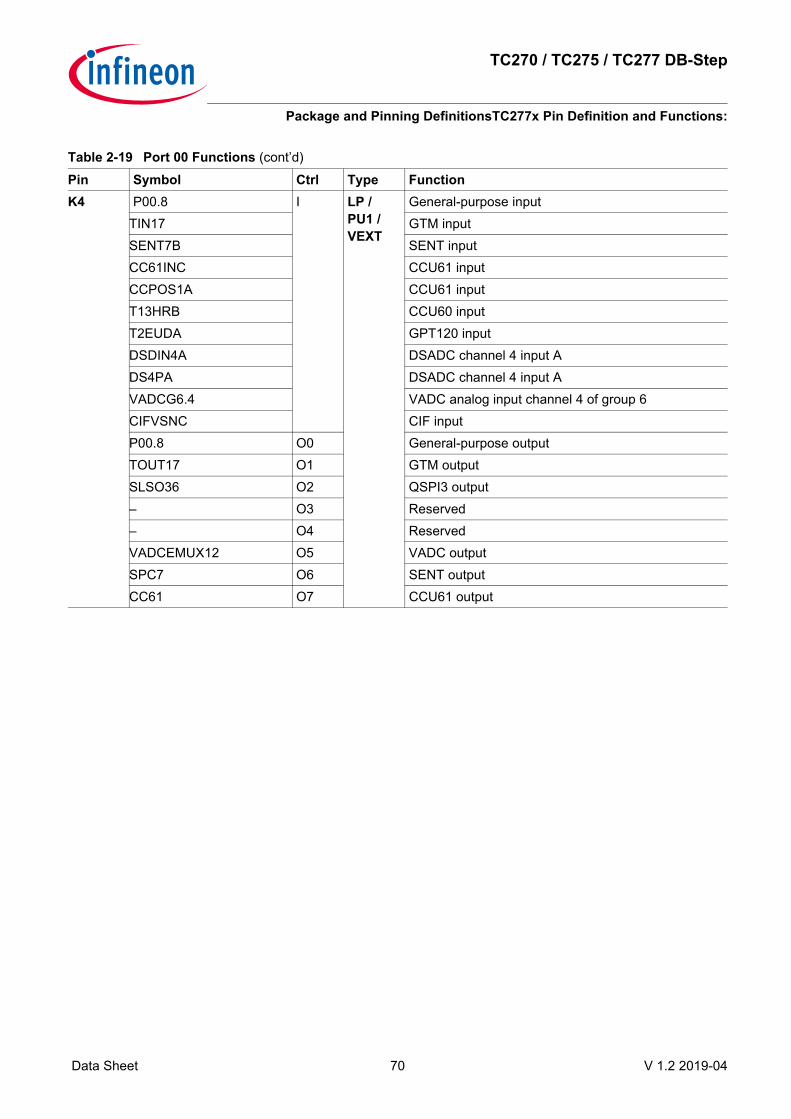
TC270 / TC275 / TC277 DB-Step
Package and Pinning DefinitionsTC277x Pin Definition and Functions:
Data Sheet 70 V 1.2 2019-04
K4 P00.8 I LP /PU1 /VEXT
General-purpose inputTIN17 GTM inputSENT7B SENT inputCC61INC CCU61 inputCCPOS1A CCU61 inputT13HRB CCU60 inputT2EUDA GPT120 inputDSDIN4A DSADC channel 4 input ADS4PA DSADC channel 4 input AVADCG6.4 VADC analog input channel 4 of group 6CIFVSNC CIF inputP00.8 O0 General-purpose outputTOUT17 O1 GTM outputSLSO36 O2 QSPI3 output– O3 Reserved– O4 ReservedVADCEMUX12 O5 VADC outputSPC7 O6 SENT outputCC61 O7 CCU61 output
Table 2-19 Port 00 Functions (cont’d)Pin Symbol Ctrl Type Function

TC270 / TC275 / TC277 DB-Step
Package and Pinning DefinitionsTC277x Pin Definition and Functions:
Data Sheet 71 V 1.2 2019-04
K2 P00.9 I LP /PU1 /VEXT
General-purpose inputTIN18 GTM inputSENT8B SENT inputCC62INC CCU61 inputCCPOS2A CCU61 inputT13HRC CCU60 inputT12HRC CCU60 inputT4EUDA GPT120 inputDSCIN1A DSADC channel 1 input AVADCG6.3 VADC analog input channel 3 of group 6DSITR3F DSADC channel 3 input FCIFHSNC CIF inputP00.9 O0 General-purpose outputTOUT18 O1 GTM outputSLSO37 O2 QSPI3 outputARTS3 O3 ASCLIN3 outputDSCOUT1 O4 DSADC channel 1 output– O5 ReservedSPC8 O6 SENT outputCC62 O7 CCU61 output
K5 P00.10 I LP /PU1 /VEXT
General-purpose inputTIN19 GTM inputSENT9B SENT inputDSDIN1A DSADC channel 1 input AVADCG6.2 VADC analog input channel 2 of group 6 (MD)P00.10 O0 General-purpose outputTOUT19 O1 GTM output– O2 Reserved– O3 Reserved– O4 Reserved– O5 ReservedSPC9 O6 SENT outputCOUT63 O7 CCU61 output
Table 2-19 Port 00 Functions (cont’d)Pin Symbol Ctrl Type Function

TC270 / TC275 / TC277 DB-Step
Package and Pinning DefinitionsTC277x Pin Definition and Functions:
Data Sheet 72 V 1.2 2019-04
L1 P00.11 I LP /PU1 /VEXT
General-purpose inputTIN20 GTM inputCTRAPA CCU60 inputT12HRE CCU61 inputDSCIN0A DSADC channel 0 input AVADCG6.1 VADC analog input channel 1 of group 6 (MD)P00.11 O0 General-purpose outputTOUT20 O1 GTM output– O2 Reserved– O3 ReservedDSCOUT0 O4 DSADC channel 0 output– O5 Reserved– O6 Reserved– O7 Reserved
L2 P00.12 I LP /PU1 /VEXT
General-purpose inputTIN21 GTM inputACTS3A ASCLIN3 inputDSDIN0A DSADC channel 0 input AVADCG6.0 VADC analog input channel 0 of group 6P00.12 O0 General-purpose outputTOUT21 O1 GTM output– O2 Reserved– O3 Reserved– O4 Reserved– O5 Reserved– O6 ReservedCOUT63 O7 CCU61 output
Table 2-19 Port 00 Functions (cont’d)Pin Symbol Ctrl Type Function

TC270 / TC275 / TC277 DB-Step
Package and Pinning DefinitionsTC277x Pin Definition and Functions:
Data Sheet 73 V 1.2 2019-04
Table 2-20 Port 01 FunctionsPin Symbol Ctrl Type FunctionG5 P01.3 I LP /
PU1 /VEXT
General-purpose inputTIN111 GTM inputSLSI3B QSPI3 inputP01.3 O0 General-purpose outputTOUT111 O1 GTM output– O2 Reserved– O3 ReservedSLSO39 O4 QSPI3 outputTXDCAN1 O5 CAN node 1 output– O6 Reserved– O7 Reserved
G4 P01.4 I LP /PU1 /VEXT
General-purpose inputTIN112 GTM inputRXDCAN1C CAN node 1 inputP01.4 O0 General-purpose outputTOUT112 O1 GTM output– O2 Reserved– O3 ReservedSLSO310 O4 QSPI3 output– O5 Reserved– O6 Reserved– O7 Reserved
H5 P01.5 I LP /PU1 /VEXT
General-purpose inputTIN113 GTM inputMRST3C QSPI3 inputP01.5 O0 General-purpose outputTOUT113 O1 GTM output– O2 Reserved– O3 ReservedMRST3 O4 QSPI3 output– O5 Reserved– O6 Reserved– O7 Reserved

TC270 / TC275 / TC277 DB-Step
Package and Pinning DefinitionsTC277x Pin Definition and Functions:
Data Sheet 74 V 1.2 2019-04
H4 P01.6 I LP /PU1 /VEXT
General-purpose inputTIN114 GTM inputMTSR3C QSPI3 inputP01.6 O0 General-purpose outputTOUT114 O1 GTM output– O2 Reserved– O3 ReservedMTSR3 O4 QSPI3 output– O5 Reserved– O6 Reserved– O7 Reserved
J5 P01.7 I LP /PU1 /VEXT
General-purpose inputTIN115 GTM inputSCLK3C QSPI3 inputP01.7 O0 General-purpose outputTOUT115 O1 GTM output– O2 Reserved– O3 ReservedSCLK3 O4 QSPI3 output– O5 Reserved– O6 Reserved– O7 Reserved
Table 2-20 Port 01 Functions (cont’d)Pin Symbol Ctrl Type Function
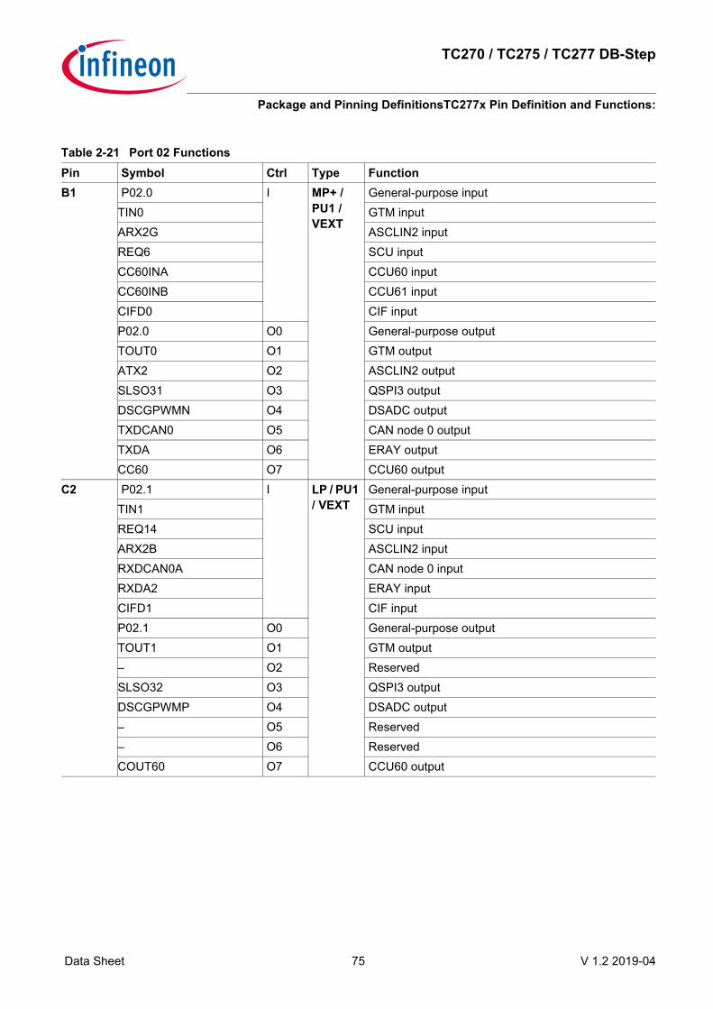
TC270 / TC275 / TC277 DB-Step
Package and Pinning DefinitionsTC277x Pin Definition and Functions:
Data Sheet 75 V 1.2 2019-04
Table 2-21 Port 02 FunctionsPin Symbol Ctrl Type FunctionB1 P02.0 I MP+ /
PU1 / VEXT
General-purpose inputTIN0 GTM inputARX2G ASCLIN2 inputREQ6 SCU inputCC60INA CCU60 inputCC60INB CCU61 inputCIFD0 CIF inputP02.0 O0 General-purpose outputTOUT0 O1 GTM outputATX2 O2 ASCLIN2 outputSLSO31 O3 QSPI3 outputDSCGPWMN O4 DSADC outputTXDCAN0 O5 CAN node 0 outputTXDA O6 ERAY outputCC60 O7 CCU60 output
C2 P02.1 I LP / PU1 / VEXT
General-purpose inputTIN1 GTM inputREQ14 SCU inputARX2B ASCLIN2 inputRXDCAN0A CAN node 0 inputRXDA2 ERAY inputCIFD1 CIF inputP02.1 O0 General-purpose outputTOUT1 O1 GTM output– O2 ReservedSLSO32 O3 QSPI3 outputDSCGPWMP O4 DSADC output– O5 Reserved– O6 ReservedCOUT60 O7 CCU60 output

TC270 / TC275 / TC277 DB-Step
Package and Pinning DefinitionsTC277x Pin Definition and Functions:
Data Sheet 76 V 1.2 2019-04
C1 P02.2 I MP+ /PU1 /VEXT
General-purpose inputTIN2 GTM inputCC61INA CCU60 inputCC61INB CCU61 inputCIFD2 CIF inputP02.2 O0 General-purpose outputTOUT2 O1 GTM outputATX1 O2 ASCLIN1 outputSLSO33 O3 QSPI3 outputPSITX0 O4 PSI5 outputTXDCAN2 O5 CAN node 2 outputTXDB O6 ERAY outputCC61 O7 CCU60 output
D2 P02.3 I LP /PU1 /VEXT
General-purpose inputTIN3 GTM inputARX1G ASCLIN1 inputRXDCAN2B CAN node 2 inputRXDB2 ERAY inputPSIRX0B PSI5 inputDSCIN5B DSADC channel 5 input BSDI11 MSC1 inputCIFD3 CIF inputP02.3 O0 General-purpose outputTOUT3 O1 GTM outputASLSO2 O2 ASCLIN2 outputSLSO34 O3 QSPI3 outputDSCOUT5 O4 DSADC channel 5 output– O5 Reserved– O6 ReservedCOUT61 O7 CCU60 output
Table 2-21 Port 02 Functions (cont’d)Pin Symbol Ctrl Type Function

TC270 / TC275 / TC277 DB-Step
Package and Pinning DefinitionsTC277x Pin Definition and Functions:
Data Sheet 77 V 1.2 2019-04
D1 P02.4 I MP+ / PU1 /VEXT
General-purpose inputTIN4 GTM inputSLSI3A QSPI3 inputECTT1 TTCAN inputRXDCAN0D CAN node 0 inputCC62INA CCU60 inputCC62INB CCU61 inputDSDIN5B DSADC channel 5 input BSDA0A I2C0 inputCIFD4 CIF inputP02.4 O0 General-purpose outputTOUT4 O1 GTM outputASCLK2 O2 ASCLIN2 outputSLSO30 O3 QSPI3 outputPSISCLK O4 PSI5-S outputSDA0 O5 I2C0 outputTXENA O6 ERAY outputCC62 O7 CCU60 output
E2 P02.5 I MP+ /PU1 /VEXT
General-purpose inputTIN5 GTM inputMRST3A QSPI3 inputECTT2 TTCAN inputPSIRX1B PSI5 inputPSISRXB PSI5-S inputSENT3C SENT inputDSCIN4B DSADC channel 4 input BSCL0A I2C0 inputCIFD5 CIF inputP02.5 O0 General-purpose outputTOUT5 O1 GTM outputTXDCAN0 O2 CAN node 0 outputMRST3 O3 QSPI3 outputDSCOUT4 O4 DSADC channel 4 outputSCL0 O5 I2C0 outputTXENB O6 ERAY outputCOUT62 O7 CCU60 output
Table 2-21 Port 02 Functions (cont’d)Pin Symbol Ctrl Type Function

TC270 / TC275 / TC277 DB-Step
Package and Pinning DefinitionsTC277x Pin Definition and Functions:
Data Sheet 78 V 1.2 2019-04
E1 P02.6 I MP / PU1 /VEXT
General-purpose inputTIN6 GTM inputMTSR3A QSPI3 inputSENT2C SENT inputCC60INC CCU60 inputCCPOS0A CCU60 inputT12HRB CCU61 inputT3INA GPT120 inputCIFD6 CIF inputDSDIN4B DSADC channel 4 input BDSITR5E DSADC channel 5 input EP02.6 O0 General-purpose outputTOUT6 O1 GTM outputPSISTX O2 PSI5-S outputMTSR3 O3 QSPI3 outputPSITX1 O4 PSI5 outputVADCEMUX00 O5 VADC output– O6 ReservedCC60 O7 CCU60 output
Table 2-21 Port 02 Functions (cont’d)Pin Symbol Ctrl Type Function

TC270 / TC275 / TC277 DB-Step
Package and Pinning DefinitionsTC277x Pin Definition and Functions:
Data Sheet 79 V 1.2 2019-04
F2 P02.7 I MP /PU1 /VEXT
General-purpose inputTIN7 GTM inputSCLK3A QSPI3 inputPSIRX2B PSI5 inputSENT1C SENT inputCC61INC CCU60 inputCCPOS1A CCU60 inputT13HRB CCU61 inputT3EUDA GPT120 inputCIFD7 CIF inputDSCIN3B DSADC channel 3 input BDSITR4E DSADC channel 4 input EP02.7 O0 General-purpose outputTOUT7 O1 GTM output– O2 ReservedSCLK3 O3 QSPI3 outputDSCOUT3 O4 DSADC channel 3 outputVADCEMUX01 O5 VADC outputSPC1 O6 SENT outputCC61 O7 CCU60 output
Table 2-21 Port 02 Functions (cont’d)Pin Symbol Ctrl Type Function

TC270 / TC275 / TC277 DB-Step
Package and Pinning DefinitionsTC277x Pin Definition and Functions:
Data Sheet 80 V 1.2 2019-04
F1 P02.8 I LP / PU1 /VEXT
General-purpose inputTIN8 GTM inputSENT0C SENT inputCC62INC CCU60 inputCCPOS2A CCU60 inputT12HRC CCU61 inputT13HRC CCU61 inputT4INA GPT120 inputCIFD8 CIF inputDSDIN3B DSADC channel 3 input BDSITR3E DSADC channel 3 input EP02.8 O0 General-purpose outputTOUT8 O1 GTM outputSLSO35 O2 QSPI3 output– O3 ReservedPSITX2 O4 PSI5 outputVADCEMUX02 O5 VADC outputETHMDC O6 ETH outputCC62 O7 CCU60 output
E4 P02.9 I LP /PU1 /VEXT
General-purpose inputTIN116 GTM inputP02.9 O0 General-purpose outputTOUT116 O1 GTM outputATX2 O2 ASCLIN2 output– O3 Reserved– O4 ReservedTXDCAN1 O5 CAN node 1 output– O6 Reserved– O7 Reserved
Table 2-21 Port 02 Functions (cont’d)Pin Symbol Ctrl Type Function
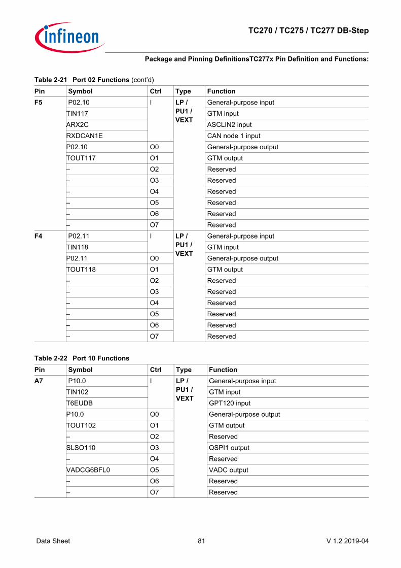
TC270 / TC275 / TC277 DB-Step
Package and Pinning DefinitionsTC277x Pin Definition and Functions:
Data Sheet 81 V 1.2 2019-04
F5 P02.10 I LP /PU1 /VEXT
General-purpose inputTIN117 GTM inputARX2C ASCLIN2 inputRXDCAN1E CAN node 1 inputP02.10 O0 General-purpose outputTOUT117 O1 GTM output– O2 Reserved– O3 Reserved– O4 Reserved– O5 Reserved– O6 Reserved– O7 Reserved
F4 P02.11 I LP /PU1 /VEXT
General-purpose inputTIN118 GTM inputP02.11 O0 General-purpose outputTOUT118 O1 GTM output– O2 Reserved– O3 Reserved– O4 Reserved– O5 Reserved– O6 Reserved– O7 Reserved
Table 2-22 Port 10 FunctionsPin Symbol Ctrl Type FunctionA7 P10.0 I LP /
PU1 /VEXT
General-purpose inputTIN102 GTM inputT6EUDB GPT120 inputP10.0 O0 General-purpose outputTOUT102 O1 GTM output– O2 ReservedSLSO110 O3 QSPI1 output– O4 ReservedVADCG6BFL0 O5 VADC output– O6 Reserved– O7 Reserved
Table 2-21 Port 02 Functions (cont’d)Pin Symbol Ctrl Type Function

TC270 / TC275 / TC277 DB-Step
Package and Pinning DefinitionsTC277x Pin Definition and Functions:
Data Sheet 82 V 1.2 2019-04
B7 P10.1 I MP+ /PU1 /VEXT
General-purpose inputTIN103 GTM inputMRST1A QSPI1 inputT5EUDB GPT120 inputP10.1 O0 General-purpose outputTOUT103 O1 GTM outputMTSR1 O2 QSPI1 outputMRST1 O3 QSPI1 outputEN01 O4 MSC0 outputVADCG6BFL1 O5 VADC outputEND03 O6 MSC0 output– O7 Reserved
A5 P10.2 I MP /PU1 /VEXT
General-purpose inputTIN104 GTM inputSCLK1A QSPI1 inputT6INB GPT120 inputREQ2 SCU inputRXDCAN2E CAN node 2 inputSDI01 MSC0 inputP10.2 O0 General-purpose outputTOUT104 O1 GTM output– O2 ReservedSCLK1 O3 QSPI1 outputEN00 O4 MSC0 outputVADCG6BFL2 O5 VADC outputEND02 O6 MSC0 output– O7 Reserved
Table 2-22 Port 10 Functions (cont’d)Pin Symbol Ctrl Type Function

TC270 / TC275 / TC277 DB-Step
Package and Pinning DefinitionsTC277x Pin Definition and Functions:
Data Sheet 83 V 1.2 2019-04
A6 P10.3 I MP /PU1 /VEXT
General-purpose inputTIN105 GTM inputMTSR1A QSPI1 inputREQ3 SCU inputT5INB GPT120 inputP10.3 O0 General-purpose outputTOUT105 O1 GTM outputVADCG6BFL3 O2 VADC outputMTSR1 O3 QSPI1 outputEN00 O4 MSC0 outputEND02 O5 MSC0 outputTXDCAN2 O6 CAN node 2 output– O7 Reserved
B6 P10.4 I MP+ /PU1 /VEXT
General-purpose inputTIN106 GTM inputMTSR1C QSPI1 inputCCPOS0C CCU60 inputT3INB GPT120 inputP10.4 O0 General-purpose outputTOUT106 O1 GTM output– O2 ReservedSLSO18 O3 QSPI1 outputMTSR1 O4 QSPI1 outputEN00 O5 MSC0 outputEND02 O6 MSC0 output– O7 Reserved
B5 P10.5 I LP /PU1 /VEXT
General-purpose inputTIN107 GTM inputHWCFG4 SCU inputINJ01 MSC0 inputP10.5 O0 General-purpose outputTOUT107 O1 GTM outputATX2 O2 ASCLIN2 outputSLSO38 O3 QSPI3 outputSLSO19 O4 QSPI1 outputT6OUT O5 GPT120 outputASLSO2 O6 ASCLIN2 output- O7 Reserved
Table 2-22 Port 10 Functions (cont’d)Pin Symbol Ctrl Type Function

TC270 / TC275 / TC277 DB-Step
Package and Pinning DefinitionsTC277x Pin Definition and Functions:
Data Sheet 84 V 1.2 2019-04
A4 P10.6 I LP /PU1 /VEXT
General-purpose inputTIN108 GTM inputARX2D ASCLIN2 inputMTSR3B QSPI3 inputHWCFG5 SCU inputP10.6 O0 General-purpose outputTOUT108 O1 GTM outputASCLK2 O2 ASCLIN2 outputMTSR3 O3 QSPI3 outputT3OUT O4 GPT120 output- O5 ReservedMRST1 O6 QSPI1 outputVADCG7BFL0 O7 VADC output
A3 P10.7 I LP /PU1 /VEXT
General-purpose inputTIN109 GTM inputACTS2A ASCLIN2 inputMRST3B QSPI3 inputREQ4 SCU inputCCPOS1C CCU60 inputT3EUDB GPT120 inputP10.7 O0 General-purpose outputTOUT109 O1 GTM output– O2 ReservedMRST3 O3 QSPI3 outputVADCG7BFL1 O4 VADC output– O5 Reserved– O6 Reserved– O7 Reserved
Table 2-22 Port 10 Functions (cont’d)Pin Symbol Ctrl Type Function

TC270 / TC275 / TC277 DB-Step
Package and Pinning DefinitionsTC277x Pin Definition and Functions:
Data Sheet 85 V 1.2 2019-04
B4 P10.8 I LP /PU1 /VEXT
General-purpose inputTIN110 GTM inputSCLK3B QSPI3 inputREQ5 SCU inputCCPOS2C CCU60 inputT4INB GPT120 inputP10.8 O0 General-purpose outputTOUT110 O1 GTM outputARTS2 O2 ASCLIN2 outputSCLK3 O3 QSPI3 output– O4 Reserved– O5 Reserved– O6 Reserved– O7 Reserved
Table 2-23 Port 11 FunctionsPin Symbol Ctrl Type FunctionE10 P11.0 I MP+ /
PU1 /VFLEX
General-purpose inputTIN119 GTM inputARX3B ASCLIN3 inputP11.0 O0 General-purpose outputTOUT119 O1 GTM outputATX3 O2 ASCLIN3 output– O3 Reserved– O4 Reserved– O5 ReservedETHTXD3 O6 ETH output– O7 Reserved
E9 P11.1 I MP+ /PU1 /VFLEX
General-purpose inputTIN120 GTM inputP11.1 O0 General-purpose outputTOUT120 O1 GTM outputASCLK3 O2 ASCLIN3 outputATX3 O3 ASCLIN3 output– O4 Reserved– O5 ReservedETHTXD2 O6 ETH output– O7 Reserved
Table 2-22 Port 10 Functions (cont’d)Pin Symbol Ctrl Type Function

TC270 / TC275 / TC277 DB-Step
Package and Pinning DefinitionsTC277x Pin Definition and Functions:
Data Sheet 86 V 1.2 2019-04
A10 P11.2 I MPR /PU1 /VFLEX
General-purpose inputTIN95 GTM inputP11.2 O0 General-purpose outputTOUT95 O1 GTM outputEND03 O2 MSC0 outputSLSO05 O3 QSPI0 outputSLSO15 O4 QSPI1 outputEN01 O5 MSC0 outputETHTXD1 O6 ETH outputCOUT63 O7 CCU60 output
B10 P11.3 I MPR /PU1 /VFLEX
General-purpose inputTIN96 GTM inputMRST1B QSPI1 inputSDI03 MSC0 inputP11.3 O0 General-purpose outputTOUT96 O1 GTM output– O2 ReservedMRST1 O3 QSPI1 outputTXDA O4 ERAY output– O5 ReservedETHTXD0 O6 ETH outputCOUT62 O7 CCU60 output
D10 P11.4 I MP+ /PU1 /VFLEX
General-purpose inputTIN121 GTM inputETHRXCLKB ETH inputP11.4 O0 General-purpose outputTOUT121 O1 GTM outputASCLK3 O2 ASCLIN3 output– O3 Reserved– O4 Reserved– O5 ReservedETHTXER O6 ETH output– O7 Reserved
Table 2-23 Port 11 Functions (cont’d)Pin Symbol Ctrl Type Function

TC270 / TC275 / TC277 DB-Step
Package and Pinning DefinitionsTC277x Pin Definition and Functions:
Data Sheet 87 V 1.2 2019-04
D8 P11.5 I LP / PU1 /VFLEX
General-purpose inputTIN122 GTM inputETHTXCLKA ETH inputP11.5 O0 General-purpose outputTOUT122 O1 GTM output– O2 Reserved– O3 Reserved– O4 Reserved– O5 Reserved– O6 Reserved– O7 Reserved
D9 P11.6 I MPR /PU1 /VFLEX
General-purpose inputTIN97 GTM inputSCLK1B QSPI1 inputP11.6 O0 General-purpose outputTOUT97 O1 GTM outputTXENB O2 ERAY outputSCLK1 O3 QSPI1 outputTXENA O4 ERAY outputFCLP0 O5 MSC0 outputETHTXEN O6 ETH outputCOUT61 O7 CCU60 output
E8 P11.7 I LP / PU1 /VFLEX
General-purpose inputTIN123 GTM inputETHRXD3 ETH inputP11.7 O0 General-purpose outputTOUT123 O1 GTM output– O2 Reserved– O3 Reserved– O4 Reserved– O5 Reserved– O6 Reserved– O7 Reserved
Table 2-23 Port 11 Functions (cont’d)Pin Symbol Ctrl Type Function

TC270 / TC275 / TC277 DB-Step
Package and Pinning DefinitionsTC277x Pin Definition and Functions:
Data Sheet 88 V 1.2 2019-04
E7 P11.8 I LP / PU1 /VFLEX
General-purpose inputTIN124 GTM inputETHRXD2 ETH inputP11.8 O0 General-purpose outputTOUT124 O1 GTM output– O2 Reserved– O3 Reserved– O4 Reserved– O5 Reserved– O6 Reserved– O7 Reserved
A9 P11.9 I MP+ /PU1 /VFLEX
General-purpose inputTIN98 GTM inputMTSR1B QSPI1 inputRXDA1 ERAY inputETHRXD1 ETH inputP11.9 O0 General-purpose outputTOUT98 O1 GTM output– O2 ReservedMTSR1 O3 QSPI1 output– O4 ReservedSOP0 O5 MSC0 output– O6 ReservedCOUT60 O7 CCU60 output
Table 2-23 Port 11 Functions (cont’d)Pin Symbol Ctrl Type Function

TC270 / TC275 / TC277 DB-Step
Package and Pinning DefinitionsTC277x Pin Definition and Functions:
Data Sheet 89 V 1.2 2019-04
B9 P11.10 I LP /PU1 /VFLEX
General-purpose inputTIN99 GTM inputREQ12 SCU inputARX1E ASCLIN1 inputSLSI1A QSPI1 inputRXDCAN3D CAN node 3 inputRXDB1 ERAY inputETHRXD0 ETH inputSDI00 MSC0 inputP11.10 O0 General-purpose outputTOUT99 O1 GTM output– O2 ReservedSLSO03 O3 QSPI0 outputSLSO13 O4 QSPI1 output– O5 Reserved– O6 ReservedCC62 O7 CCU60 output
A8 P11.11 I MP+ /PU1 /VFLEX
General-purpose inputTIN100 GTM inputETHCRSDVA ETH inputETHRXDVA ETH inputETHCRSB ETH inputP11.11 O0 General-purpose outputTOUT100 O1 GTM outputEND02 O2 MSC0 outputSLSO04 O3 QSPI0 outputSLSO14 O4 QSPI1 outputEN00 O5 MSC0 outputTXENB O6 ERAY outputCC61 O7 CCU60 output
Table 2-23 Port 11 Functions (cont’d)Pin Symbol Ctrl Type Function

TC270 / TC275 / TC277 DB-Step
Package and Pinning DefinitionsTC277x Pin Definition and Functions:
Data Sheet 90 V 1.2 2019-04
B8 P11.12 IO0
MPR /PU1 /VFLEX
General-purpose inputTIN101 GTM inputETHREFCLK ETH inputETHTXCLKB ETH input
(Not for productive purposes)P11.12 General-purpose outputTOUT101 O1 GTM outputATX1 O2 ASCLIN1 outputGTMCLK2 O3 GTM outputTXDB O4 ERAY outputTXDCAN3 O5 CAN node 3 outputEXTCLK1 O6 SCU outputCC60 O7 CCU60 output
E6 P11.13 I LP / PU1 /VFLEX
General-purpose inputTIN125 GTM inputETHRXERA ETH inputP11.13 O0 General-purpose outputTOUT125 O1 GTM output– O2 Reserved– O3 Reserved– O4 Reserved– O5 Reserved– O6 Reserved– O7 Reserved
D7 P11.14 I LP / PU1 /VFLEX
General-purpose inputTIN126 GTM inputETHCRSDVB ETH inputETHRXDVB ETH inputETHCRSA ETH inputP11.14 O0 General-purpose outputTOUT126 O1 GTM output– O2 Reserved– O3 Reserved– O4 Reserved– O5 Reserved– O6 Reserved– O7 Reserved
Table 2-23 Port 11 Functions (cont’d)Pin Symbol Ctrl Type Function

TC270 / TC275 / TC277 DB-Step
Package and Pinning DefinitionsTC277x Pin Definition and Functions:
Data Sheet 91 V 1.2 2019-04
D6 P11.15 I LP /PU1 /VFLEX
General-purpose inputTIN127 GTM inputETHCOL ETH inputP11.15 O0 General-purpose outputTOUT127 O1 GTM output– O2 Reserved– O3 Reserved– O4 Reserved– O5 Reserved– O6 Reserved– O7 Reserved
Table 2-24 Port 12 FunctionsPin Symbol Ctrl Type FunctionE12 P12.0 I LP /
PU1 /VFLEX
General-purpose inputTIN128 GTM inputETHRXCLKC ETH inputRXDCAN0C CAN node 0 inputP12.0 O0 General-purpose outputTOUT128 O1 GTM output– O2 Reserved– O3 Reserved– O4 Reserved– O5 ReservedETHMDC O6 ETH output– O7 Reserved
E11 P12.1 I LP /PU1 /VFLEX
General-purpose inputTIN129 GTM inputP12.1 O0 General-purpose outputTOUT129 O1 GTM outputASLSO3 O2 ASCLIN3 output– O3 Reserved– O4 ReservedTXDCAN0 O5 CAN node 0 output– O6 Reserved– O7 ReservedETHMDIOC HWOU
TETH input/output
Table 2-23 Port 11 Functions (cont’d)Pin Symbol Ctrl Type Function

TC270 / TC275 / TC277 DB-Step
Package and Pinning DefinitionsTC277x Pin Definition and Functions:
Data Sheet 92 V 1.2 2019-04
Table 2-25 Port 13 FunctionsPin Symbol Ctrl Type FunctionB12 P13.0 I LVDSM_N /
PU1 / VEXT
General-purpose inputTIN91 GTM inputP13.0 O0 General-purpose outputTOUT91 O1 GTM outputEND03 O2 MSC0 outputSCLK2N O3 QSPI2 output (LVDS)EN01 O4 MSC0 outputFCLN0 O5 MSC0 output (LVDS)FCLND0 O6 MSC0 output (LVDS)– O7 Reserved
A12 P13.1 I LVDSM_P /PU1 / VEXT
General-purpose inputTIN92 GTM inputSCL0B I2C0 inputP13.1 O0 General-purpose outputTOUT92 O1 GTM output– O2 ReservedSCLK2P O3 QSPI2 output (LVDS)– O4 ReservedFCLP0 O5 MSC0 output (LVDS)SCL0 O6 I2C0 output– O7 Reserved
B11 P13.2 I LVDSM_N /PU1 / VEXT
General-purpose inputTIN93 GTM inputCAPINA GPT120 inputSDA0B I2C0 inputP13.2 O0 General-purpose outputTOUT93 O1 GTM output– O2 ReservedMTSR2N O3 QSPI2 output (LVDS)FCLP0 O4 MSC0 outputSON0 O5 MSC0 output (LVDS)SDA0 O6 I2C0 outputSOND0 O7 MSC0 output (LVDS)

TC270 / TC275 / TC277 DB-Step
Package and Pinning DefinitionsTC277x Pin Definition and Functions:
Data Sheet 93 V 1.2 2019-04
A11 P13.3 I LVDSM_P /PU1 / VEXT
General-purpose inputTIN94 GTM inputP13.3 O0 General-purpose outputTOUT94 O1 GTM output– O2 ReservedMTSR2P O3 QSPI2 output (LVDS)– O4 ReservedSOP0 O5 MSC0 output (LVDS)– O6 Reserved– O7 Reserved
Table 2-26 Port 14 FunctionsPin Symbol Ctrl Type FunctionB16 P14.0 I MP+ /
PU1 /VEXT
General-purpose inputTIN80 GTM inputP14.0 O0 General-purpose outputTOUT80 O1 GTM outputATX0 O2 ASCLIN0 output
Recommended as Boot loader pin.TXDA O3 ERAY outputTXDB O4 ERAY outputTXDCAN1 O5 CAN node 1 output
Used for single pin DAP (SPD) function.ASCLK0 O6 ASCLIN0 outputCOUT62 O7 CCU60 output
Table 2-25 Port 13 Functions (cont’d)Pin Symbol Ctrl Type Function

TC270 / TC275 / TC277 DB-Step
Package and Pinning DefinitionsTC277x Pin Definition and Functions:
Data Sheet 94 V 1.2 2019-04
A15 P14.1 I MP /PU1 /VEXT
General-purpose inputTIN81 GTM inputREQ15 SCU inputARX0A ASCLIN0 input
Recommended as Boot loader pin.RXDCAN1B CAN node 1 input
Used for single pin DAP (SPD) function.RXDA3 ERAY inputRXDB3 ERAY inputEVRWUPA SCU inputP14.1 O0 General-purpose outputTOUT81 O1 GTM outputATX0 O2 ASCLIN0 output– O3 Reserved– O4 Reserved– O5 Reserved– O6 ReservedCOUT63 O7 CCU60 output
E13 P14.2 I LP /PU1 /VEXT
General-purpose inputTIN82 GTM inputHWCFG2EVR13
SCU inputLatched at cold power on reset to decide EVR13 activation.
P14.2 O0 General-purpose outputTOUT82 O1 GTM outputATX2 O2 ASCLIN2 outputSLSO21 O3 QSPI2 output– O4 Reserved– O5 ReservedASCLK2 O6 ASCLIN2 output– O7 Reserved
Table 2-26 Port 14 Functions (cont’d)Pin Symbol Ctrl Type Function

TC270 / TC275 / TC277 DB-Step
Package and Pinning DefinitionsTC277x Pin Definition and Functions:
Data Sheet 95 V 1.2 2019-04
B14 P14.3 I LP /PU1 /VEXT
General-purpose inputTIN83 GTM inputARX2A ASCLIN2 inputREQ10 SCU inputHWCFG3_BMI SCU inputSDI02 MSC0 inputP14.3 O0 General-purpose outputTOUT83 O1 GTM outputATX2 O2 ASCLIN2 outputSLSO23 O3 QSPI2 outputASLSO1 O4 ASCLIN1 outputASLSO3 O5 ASCLIN3 output– O6 Reserved– O7 Reserved
B15 P14.4 I LP /PU1 /VEXT
General-purpose inputTIN84 GTM inputHWCFG6 SCU input
Latched at cold power on reset to decide default pad reset state (PU or HighZ).
P14.4 O0 General-purpose outputTOUT84 O1 GTM output– O2 Reserved– O3 Reserved– O4 Reserved– O5 Reserved– O6 Reserved– O7 Reserved
Table 2-26 Port 14 Functions (cont’d)Pin Symbol Ctrl Type Function

TC270 / TC275 / TC277 DB-Step
Package and Pinning DefinitionsTC277x Pin Definition and Functions:
Data Sheet 96 V 1.2 2019-04
A14 P14.5 I MP+ /PU1 /VEXT
General-purpose inputTIN85 GTM inputHWCFG1EVR33
SCU inputLatched at cold power on reset to decide EVR33 activation.
P14.5 O0 General-purpose outputTOUT85 O1 GTM output– O2 Reserved– O3 Reserved– O4 Reserved– O5 ReservedTXDB O6 ERAY output– O7 Reserved
B13 P14.6 I MP+ /PU1 /VEXT
General-purpose inputTIN86 GTM inputHWCFG0DCLDO
SCU inputIf EVR13 active, latched at cold power on reset to decide between LDO and SMPS mode.
P14.6 O0 General-purpose outputTOUT86 O1 GTM output– O2 ReservedSLSO22 O3 QSPI2 output– O4 Reserved– O5 ReservedTXENB O6 ERAY output– O7 Reserved
D13 P14.7 I LP /PU1 /VEXT
General-purpose inputTIN87 GTM inputRXDB0 ERAY inputP14.7 O0 General-purpose outputTOUT87 O1 GTM outputARTS0 O2 ASCLIN0 outputSLSO24 O3 QSPI2 output– O4 Reserved– O5 Reserved– O6 Reserved– O7 Reserved
Table 2-26 Port 14 Functions (cont’d)Pin Symbol Ctrl Type Function

TC270 / TC275 / TC277 DB-Step
Package and Pinning DefinitionsTC277x Pin Definition and Functions:
Data Sheet 97 V 1.2 2019-04
A13 P14.8 I LP /PU1 /VEXT
General-purpose inputTIN88 GTM inputARX1D ASCLIN1 inputRXDCAN2D CAN node 2 inputRXDA0 ERAY inputP14.8 O0 General-purpose outputTOUT88 O1 GTM output– O2 Reserved– O3 Reserved– O4 Reserved– O5 Reserved– O6 Reserved– O7 Reserved
D12 P14.9 I MP+ /PU1 /VEXT
General-purpose inputTIN89 GTM inputACTS0A ASCLIN0 inputP14.9 O0 General-purpose outputTOUT89 O1 GTM outputEND03 O2 MSC0 outputEN01 O3 MSC0 output– O4 ReservedTXENB O5 ERAY outputTXENA O6 ERAY output– O7 Reserved
D11 P14.10 I MP+ /PU1 /VEXT
General-purpose inputTIN90 GTM inputP14.10 O0 General-purpose outputTOUT90 O1 GTM outputEND02 O2 MSC0 outputEN00 O3 MSC0 outputATX1 O4 ASCLIN1 outputTXDCAN2 O5 CAN node 2 outputTXDA O6 ERAY output– O7 Reserved
Table 2-26 Port 14 Functions (cont’d)Pin Symbol Ctrl Type Function

TC270 / TC275 / TC277 DB-Step
Package and Pinning DefinitionsTC277x Pin Definition and Functions:
Data Sheet 98 V 1.2 2019-04
Table 2-27 Port 15 FunctionsPin Symbol Ctrl Type FunctionB20 P15.0 I LP /
PU1 /VEXT
General-purpose inputTIN71 GTM inputP15.0 O0 General-purpose outputTOUT71 O1 GTM outputATX1 O2 ASCLIN1 outputSLSO013 O3 QSPI0 output– O4 ReservedTXDCAN2 O5 CAN node 2 outputASCLK1 O6 ASCLIN1 output– O7 Reserved
A18 P15.1 I LP /PU1 /VEXT
General-purpose inputTIN72 GTM inputREQ16 SCU inputARX1A ASCLIN1 inputRXDCAN2A CAN node 2 inputSLSI2B QSPI2 inputEVRWUPB SCU inputP15.1 O0 General-purpose outputTOUT72 O1 GTM outputATX1 O2 ASCLIN1 outputSLSO25 O3 QSPI2 output– O4 Reserved– O5 Reserved– O6 Reserved– O7 Reserved
C19 P15.2 I MP /PU1 /VEXT
General-purpose inputTIN73 GTM inputSLSI2A QSPI2 inputMRST2E QSPI2 inputP15.2 O0 General-purpose outputTOUT73 O1 GTM outputATX0 O2 ASCLIN0 outputSLSO20 O3 QSPI2 output– O4 ReservedTXDCAN1 O5 CAN node 1 outputASCLK0 O6 ASCLIN0 output– O7 Reserved

TC270 / TC275 / TC277 DB-Step
Package and Pinning DefinitionsTC277x Pin Definition and Functions:
Data Sheet 99 V 1.2 2019-04
B17 P15.3 I MP /PU1 /VEXT
General-purpose inputTIN74 GTM inputARX0B ASCLIN0 inputSCLK2A QSPI2 inputRXDCAN1A CAN node 1 inputP15.3 O0 General-purpose outputTOUT74 O1 GTM outputATX0 O2 ASCLIN0 outputSCLK2 O3 QSPI2 outputEND03 O4 MSC0 outputEN01 O5 MSC0 output– O6 Reserved– O7 Reserved
A17 P15.4 I MP /PU1 /VEXT
General-purpose inputTIN75 GTM inputMRST2A QSPI2 inputREQ0 SCU inputSCL0C I2C0 inputP15.4 O0 General-purpose outputTOUT75 O1 GTM outputATX1 O2 ASCLIN1 outputMRST2 O3 QSPI2 output– O4 Reserved– O5 ReservedSCL0 O6 I2C0 outputCC62 O7 CCU60 output
Table 2-27 Port 15 Functions (cont’d)Pin Symbol Ctrl Type Function

TC270 / TC275 / TC277 DB-Step
Package and Pinning DefinitionsTC277x Pin Definition and Functions:
Data Sheet 100 V 1.2 2019-04
E14 P15.5 I MP /PU1 /VEXT
General-purpose inputTIN76 GTM inputARX1B ASCLIN1 inputMTSR2A QSPI2 inputREQ13 SCU inputSDA0C I2C0 inputP15.5 O0 General-purpose outputTOUT76 O1 GTM outputATX1 O2 ASCLIN1 outputMTSR2 O3 QSPI2 outputEND02 O4 MSC0 outputEN00 O5 MSC0 outputSDA0 O6 I2C0 outputCC61 O7 CCU60 output
A16 P15.6 I MP /PU1 /VEXT
General-purpose inputTIN77 GTM inputMTSR2B QSPI2 inputP15.6 O0 General-purpose outputTOUT77 O1 GTM outputATX3 O2 ASCLIN3 outputMTSR2 O3 QSPI2 output– O4 ReservedSCLK2 O5 QSPI2 outputASCLK3 O6 ASCLIN3 outputCC60 O7 CCU60 output
D15 P15.7 I MP /PU1 /VEXT
General-purpose inputTIN78 GTM inputARX3A ASCLIN3 inputMRST2B QSPI2 inputP15.7 O0 General-purpose outputTOUT78 O1 GTM outputATX3 O2 ASCLIN3 outputMRST2 O3 QSPI2 output– O4 Reserved– O5 Reserved– O6 ReservedCOUT60 O7 CCU60 output
Table 2-27 Port 15 Functions (cont’d)Pin Symbol Ctrl Type Function
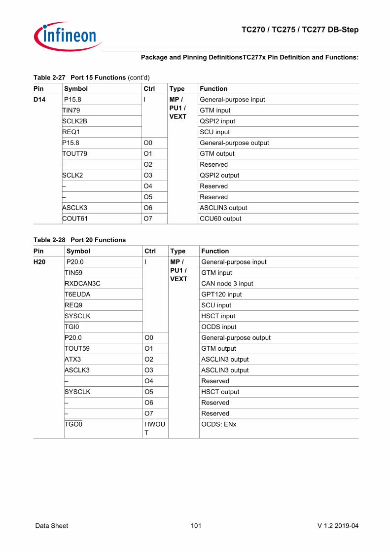
TC270 / TC275 / TC277 DB-Step
Package and Pinning DefinitionsTC277x Pin Definition and Functions:
Data Sheet 101 V 1.2 2019-04
D14 P15.8 I MP /PU1 /VEXT
General-purpose inputTIN79 GTM inputSCLK2B QSPI2 inputREQ1 SCU inputP15.8 O0 General-purpose outputTOUT79 O1 GTM output– O2 ReservedSCLK2 O3 QSPI2 output– O4 Reserved– O5 ReservedASCLK3 O6 ASCLIN3 outputCOUT61 O7 CCU60 output
Table 2-28 Port 20 FunctionsPin Symbol Ctrl Type FunctionH20 P20.0 I MP /
PU1 /VEXT
General-purpose inputTIN59 GTM inputRXDCAN3C CAN node 3 inputT6EUDA GPT120 inputREQ9 SCU inputSYSCLK HSCT inputTGI0 OCDS inputP20.0 O0 General-purpose outputTOUT59 O1 GTM outputATX3 O2 ASCLIN3 outputASCLK3 O3 ASCLIN3 output– O4 ReservedSYSCLK O5 HSCT output– O6 Reserved– O7 ReservedTGO0 HWOU
TOCDS; ENx
Table 2-27 Port 15 Functions (cont’d)Pin Symbol Ctrl Type Function

TC270 / TC275 / TC277 DB-Step
Package and Pinning DefinitionsTC277x Pin Definition and Functions:
Data Sheet 102 V 1.2 2019-04
G19 P20.1 I LP /PU1 /VEXT
General-purpose inputTIN60 GTM inputTGI1 OCDS inputP20.1 O0 General-purpose outputTOUT60 O1 GTM output– O2 Reserved– O3 Reserved– O4 Reserved– O5 Reserved– O6 Reserved– O7 ReservedTGO1 HWOU
TOCDS; ENx
H19 P20.2 I LP /PU /VEXT
General-purpose inputThis pin is latched at power on reset release to enter test mode.
TESTMODE OCDS inputP20.2 O0 Output function not available– O1 Output function not available– O2 Output function not available– O3 Output function not available– O4 Output function not available– O5 Output function not available– O6 Output function not available– O7 Output function not available
G20 P20.3 I LP /PU1 /VEXT
General-purpose inputTIN61 GTM inputT6INA GPT120 inputARX3C ASCLIN3 inputP20.3 O0 General-purpose outputTOUT61 O1 GTM outputATX3 O2 ASCLIN3 outputSLSO09 O3 QSPI0 outputSLSO29 O4 QSPI2 outputTXDCAN3 O5 CAN node 3 output– O6 Reserved– O7 Reserved
Table 2-28 Port 20 Functions (cont’d)Pin Symbol Ctrl Type Function

TC270 / TC275 / TC277 DB-Step
Package and Pinning DefinitionsTC277x Pin Definition and Functions:
Data Sheet 103 V 1.2 2019-04
F17 P20.6 I LP /PU1 /VEXT
General-purpose inputTIN62 GTM inputP20.6 O0 General-purpose outputTOUT62 O1 GTM outputARTS1 O2 ASCLIN1 outputSLSO08 O3 QSPI0 outputSLSO28 O4 QSPI2 output– O5 ReservedWDT2LCK O6 SCU output– O7 Reserved
F19 P20.7 I LP /PU1 /VEXT
General-purpose inputTIN63 GTM inputACTS1A ASCLIN1 inputRXDCAN0B CAN node 0 inputP20.7 O0 General-purpose outputTOUT63 O1 GTM output– O2 Reserved– O3 Reserved– O4 Reserved– O5 ReservedWDT1LCK O6 SCU outputCOUT63 O7 CCU61 output
F20 P20.8 I MP /PU1 /VEXT
General-purpose inputTIN64 GTM inputP20.8 O0 General-purpose outputTOUT64 O1 GTM outputASLSO1 O2 ASCLIN1 outputSLSO00 O3 QSPI0 outputSLSO10 O4 QSPI1 outputTXDCAN0 O5 CAN node 0 outputWDT0LCK O6 SCU outputCC60 O7 CCU61 output
Table 2-28 Port 20 Functions (cont’d)Pin Symbol Ctrl Type Function

TC270 / TC275 / TC277 DB-Step
Package and Pinning DefinitionsTC277x Pin Definition and Functions:
Data Sheet 104 V 1.2 2019-04
E17 P20.9 I LP /PU1 /VEXT
General-purpose inputTIN65 GTM inputARX1C ASCLIN1 inputRXDCAN3E CAN node 3 inputREQ11 SCU inputSLSI0B QSPI0 inputP20.9 O0 General-purpose outputTOUT65 O1 GTM output– O2 ReservedSLSO01 O3 QSPI0 outputSLSO11 O4 QSPI1 output– O5 ReservedWDTSLCK O6 SCU outputCC61 O7 CCU61 output
E19 P20.10 I MP /PU1 /VEXT
General-purpose inputTIN66 GTM inputP20.10 O0 General-purpose outputTOUT66 O1 GTM outputATX1 O2 ASCLIN1 outputSLSO06 O3 QSPI0 outputSLSO27 O4 QSPI2 outputTXDCAN3 O5 CAN node 3 outputASCLK1 O6 ASCLIN1 outputCC62 O7 CCU61 output
E20 P20.11 I MP /PU1 /VEXT
General-purpose inputTIN67 GTM inputSCLK0A QSPI0 inputP20.11 O0 General-purpose outputTOUT67 O1 GTM output– O2 ReservedSCLK0 O3 QSPI0 output– O4 Reserved– O5 Reserved– O6 ReservedCOUT60 O7 CCU61 output
Table 2-28 Port 20 Functions (cont’d)Pin Symbol Ctrl Type Function
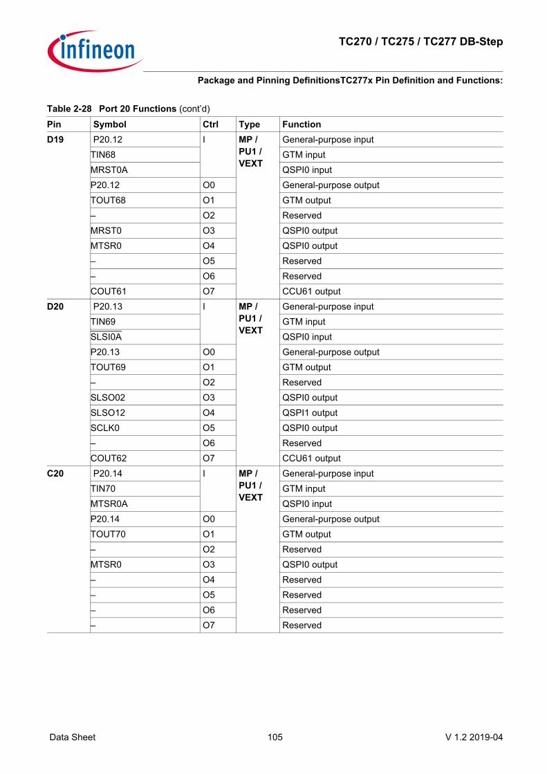
TC270 / TC275 / TC277 DB-Step
Package and Pinning DefinitionsTC277x Pin Definition and Functions:
Data Sheet 105 V 1.2 2019-04
D19 P20.12 I MP /PU1 /VEXT
General-purpose inputTIN68 GTM inputMRST0A QSPI0 inputP20.12 O0 General-purpose outputTOUT68 O1 GTM output– O2 ReservedMRST0 O3 QSPI0 outputMTSR0 O4 QSPI0 output– O5 Reserved– O6 ReservedCOUT61 O7 CCU61 output
D20 P20.13 I MP /PU1 /VEXT
General-purpose inputTIN69 GTM inputSLSI0A QSPI0 inputP20.13 O0 General-purpose outputTOUT69 O1 GTM output– O2 ReservedSLSO02 O3 QSPI0 outputSLSO12 O4 QSPI1 outputSCLK0 O5 QSPI0 output– O6 ReservedCOUT62 O7 CCU61 output
C20 P20.14 I MP /PU1 /VEXT
General-purpose inputTIN70 GTM inputMTSR0A QSPI0 inputP20.14 O0 General-purpose outputTOUT70 O1 GTM output– O2 ReservedMTSR0 O3 QSPI0 output– O4 Reserved– O5 Reserved– O6 Reserved– O7 Reserved
Table 2-28 Port 20 Functions (cont’d)Pin Symbol Ctrl Type Function

TC270 / TC275 / TC277 DB-Step
Package and Pinning DefinitionsTC277x Pin Definition and Functions:
Data Sheet 106 V 1.2 2019-04
Table 2-29 Port 21 FunctionsPin Symbol Ctrl Type FunctionK17 P21.0 I A2 /
PU1 /VDDP3
General-purpose inputTIN51 GTM inputP21.0 O0 General-purpose outputTOUT51 O1 GTM output– O2 Reserved– O3 Reserved– O4 Reserved– O5 ReservedETHMDC O6 ETH output– O7 ReservedHSM1 HWOU
THSM output 1
J17 P21.1 I A2 / PU1 /VDDP3
General-purpose inputTIN52 GTM inputETHMDIOB ETH input
(Not for production purposes)P21.1 O0 General-purpose outputTOUT52 O1 GTM output– O2 Reserved– O3 Reserved– O4 Reserved– O5 ReservedETHMDIO O6 ETH output
(Not for production purposes)– O7 ReservedHSM2 HWOU
THSM output 2

TC270 / TC275 / TC277 DB-Step
Package and Pinning DefinitionsTC277x Pin Definition and Functions:
Data Sheet 107 V 1.2 2019-04
K19 P21.2 I LVDSH_N/ PU1 /VDDP3
General-purpose inputTIN53 GTM inputMRST2CN QSPI2 input (LVDS)MRST3FN QSPI3 input (LVDS)ARX3GN ASCLIN3 input (LVDS)EMGSTOPB SCU inputRXDN HSCT input (LVDS)P21.2 O0 General-purpose outputTOUT53 O1 GTM outputASLSO3 O2 ASCLIN3 output– O3 Reserved– O4 ReservedETHMDC O5 ETH output– O6 Reserved– O7 Reserved
J19 P21.3 I LVDSH_P/ PU1 /VDDP3
General-purpose inputTIN54 GTM inputMRST2CP QSPI2 input (LVDS)MRST3FP QSPI3 input (LVDS)ARX3GP ASCLIN3 input (LVDS)RXDP HSCT input (LVDS)P21.3 O0 General-purpose outputTOUT54 O1 GTM output– O2 Reserved– O3 Reserved– O4 Reserved– O5 Reserved– O6 Reserved– O7 ReservedETHMDIOD HWOU
TETH input/output
Table 2-29 Port 21 Functions (cont’d)Pin Symbol Ctrl Type Function

TC270 / TC275 / TC277 DB-Step
Package and Pinning DefinitionsTC277x Pin Definition and Functions:
Data Sheet 108 V 1.2 2019-04
K20 P21.4 I LVDSH_N/ PU1 /VDDP3
General-purpose inputTIN55 GTM inputP21.4 O0 General-purpose outputTOUT55 O1 GTM output– O2 Reserved– O3 Reserved– O4 Reserved– O5 Reserved– O6 Reserved– O7 ReservedTXDN HSCT HSCT output (LVDS)
J20 P21.5 I LVDSH_P/ PU1 /VDDP3
General-purpose inputTIN56 GTM inputP21.5 O0 General-purpose outputTOUT56 O1 GTM outputASCLK3 O2 ASCLIN3 output– O3 Reserved– O4 Reserved– O5 Reserved– O6 Reserved– O7 ReservedTXDP HSCT HSCT output (LVDS)
H17 P21.6 I A2 / PU /VDDP3
General-purpose inputTIN57 GTM inputARX3F ASCLIN3 inputTGI2 OCDS inputTDI OCDS (JTAG) inputT5EUDA GPT120 inputP21.6 O0 General-purpose outputTOUT57 O1 GTM outputASLSO3 O2 ASCLIN3 output– O3 Reserved– O4 ReservedSYSCLK O5 HSCT output– O6 ReservedT3OUT O7 GPT120 outputTGO2 HWOU
TOCDS; ENx
Table 2-29 Port 21 Functions (cont’d)Pin Symbol Ctrl Type Function

TC270 / TC275 / TC277 DB-Step
Package and Pinning DefinitionsTC277x Pin Definition and Functions:
Data Sheet 109 V 1.2 2019-04
H16 P21.7 I A2 / PU /VDDP3
General-purpose inputTIN58 GTM inputDAP2 OCDS inputTGI3 OCDS inputTDO OCDS (JTAG) input
The JTAG TDO function is overlayed with P21.7 via a double bond. In JTAG mode this pin is used as TDO, after power-on reset it is HighZ. In DAP mode this pin is used as P21.7 and controlled by the related port control logic
ETHRXERB ETH inputT5INA GPT120 inputP21.7 O0 General-purpose outputTOUT58 O1 GTM outputATX3 O2 ASCLIN3 outputASCLK3 O3 ASCLIN3 output– O4 Reserved– O5 Reserved– O6 ReservedT6OUT O7 GPT120 outputTGO3 HWOU
TOCDS; ENx
TDO OCDS (JTAG); ENxThe JTAG TDO function is overlayed with P21.7 via a double bond. In JTAG mode this pin is used as TDO, after power-on reset it is HighZ. In DAP mode this pin is used as P21.7 and controlled by the related port control logic
Table 2-29 Port 21 Functions (cont’d)Pin Symbol Ctrl Type Function

TC270 / TC275 / TC277 DB-Step
Package and Pinning DefinitionsTC277x Pin Definition and Functions:
Data Sheet 110 V 1.2 2019-04
Table 2-30 Port 22 FunctionsPin Symbol Ctrl Type FunctionP20 P22.0 I LVDSM_N /
PU1 / VEXT
General-purpose inputTIN47 GTM inputMTSR3E QSPI3 inputP22.0 O0 General-purpose outputTOUT47 O1 GTM outputATX3N O2 ASCLIN3 output (LVDS)MTSR3 O3 QSPI3 outputSCLK3N O4 QSPI3 output (LVDS)FCLN1 O5 MSC1 output (LVDS)FCLND1 O6 MSC1 output (LVDS)– O7 Reserved
P19 P22.1 I LVDSM_P /PU1 / VEXT
General-purpose inputTIN48 GTM inputMRST3E QSPI3 inputP22.1 O0 General-purpose outputTOUT48 O1 GTM outputATX3P O2 ASCLIN3 output (LVDS)MRST3 O3 QSPI3 outputSCLK3P O4 QSPI3 output (LVDS)FCLP1 O5 MSC1 output (LVDS)– O6 Reserved– O7 Reserved
R20 P22.2 I LVDSM_N /PU1 / VEXT
General-purpose inputTIN49 GTM inputSLSI3D QSPI3 inputP22.2 O0 General-purpose outputTOUT49 O1 GTM output– O2 ReservedSLSO312 O3 QSPI3 outputMTSR3N O4 QSPI3 output (LVDS)SON1 O5 MSC1 output (LVDS)SOND1 O6 MSC1 output (LVDS)– O7 Reserved

TC270 / TC275 / TC277 DB-Step
Package and Pinning DefinitionsTC277x Pin Definition and Functions:
Data Sheet 111 V 1.2 2019-04
R19 P22.3 I LVDSM_P /PU1 / VEXT
General-purpose inputTIN50 GTM inputSCLK3E QSPI3 inputP22.3 O0 General-purpose outputTOUT50 O1 GTM output– O2 ReservedSCLK3 O3 QSPI3 outputMTSR3P O4 QSPI3 output (LVDS)SOP1 O5 MSC1 output (LVDS)– O6 Reserved– O7 Reserved
P16 P22.4 I LP / PU1 /VEXT
General-purpose inputTIN130 GTM inputP22.4 O0 General-purpose outputTOUT130 O1 GTM output– O2 Reserved– O3 ReservedSLSO012 O4 QSPI0 output– O5 Reserved– O6 Reserved– O7 Reserved
P17 P22.5 I LP / PU1 /VEXT
General-purpose inputTIN131 GTM inputMTSR0C QSPI0 inputP22.5 O0 General-purpose outputTOUT131 O1 GTM output– O2 Reserved– O3 ReservedMTSR0 O4 QSPI0 output– O5 Reserved– O6 Reserved– O7 Reserved
Table 2-30 Port 22 Functions (cont’d)Pin Symbol Ctrl Type Function

TC270 / TC275 / TC277 DB-Step
Package and Pinning DefinitionsTC277x Pin Definition and Functions:
Data Sheet 112 V 1.2 2019-04
N16 P22.6 I LP / PU1 /VEXT
General-purpose inputTIN132 GTM inputMRST0C QSPI0 inputP22.6 O0 General-purpose outputTOUT132 O1 GTM output– O2 Reserved– O3 ReservedMRST0 O4 QSPI0 output– O5 Reserved– O6 Reserved– O7 Reserved
N17 P22.7 I LP / PU1 /VEXT
General-purpose inputTIN133 GTM inputSCLK0C QSPI0 inputP22.7 O0 General-purpose outputTOUT133 O1 GTM output– O2 Reserved– O3 ReservedSCLK0 O4 QSPI0 output– O5 Reserved– O6 Reserved– O7 Reserved
M16 P22.8 I LP / PU1 /VEXT
General-purpose inputTIN134 GTM inputSCLK0B QSPI0 inputP22.8 O0 General-purpose outputTOUT134 O1 GTM output– O2 Reserved– O3 ReservedSCLK0 O4 QSPI0 output– O5 Reserved– O6 Reserved– O7 Reserved
Table 2-30 Port 22 Functions (cont’d)Pin Symbol Ctrl Type Function

TC270 / TC275 / TC277 DB-Step
Package and Pinning DefinitionsTC277x Pin Definition and Functions:
Data Sheet 113 V 1.2 2019-04
M17 P22.9 I LP / PU1 /VEXT
General-purpose inputTIN135 GTM inputMRST0B QSPI0 inputP22.9 O0 General-purpose outputTOUT135 O1 GTM output– O2 Reserved– O3 ReservedMRST0 O4 QSPI0 output– O5 Reserved– O6 Reserved– O7 Reserved
L16 P22.10 I LP / PU1 /VEXT
General-purpose inputTIN136 GTM inputMTSR0B QSPI0 inputP22.10 O0 General-purpose outputTOUT136 O1 GTM output– O2 Reserved– O3 ReservedMTSR0 O4 QSPI0 output– O5 Reserved– O6 Reserved– O7 Reserved
L17 P22.11 I LP / PU1 /VEXT
General-purpose inputTIN137 GTM inputP22.11 O0 General-purpose outputTOUT137 O1 GTM output– O2 Reserved– O3 ReservedSLSO010 O4 QSPI0 output– O5 Reserved– O6 Reserved– O7 Reserved
Table 2-30 Port 22 Functions (cont’d)Pin Symbol Ctrl Type Function

TC270 / TC275 / TC277 DB-Step
Package and Pinning DefinitionsTC277x Pin Definition and Functions:
Data Sheet 114 V 1.2 2019-04
Table 2-31 Port 23 FunctionsPin Symbol Ctrl Type FunctionV20 P23.0 I LP /
PU1 /VEXT
General-purpose inputTIN41 GTM inputP23.0 O0 General-purpose outputTOUT41 O1 GTM output– O2 Reserved– O3 Reserved– O4 Reserved– O5 Reserved– O6 Reserved– O7 Reserved
U19 P23.1 I MP+ /PU1 /VEXT
General-purpose inputTIN42 GTM inputSDI10 MSC1 inputP23.1 O0 General-purpose outputTOUT42 O1 GTM outputARTS1 O2 ASCLIN1 outputSLSO313 O3 QSPI3 outputGTMCLK0 O4 GTM output– O5 ReservedEXTCLK0 O6 SCU output– O7 Reserved
U20 P23.2 I LP /PU1 /VEXT
General-purpose inputTIN43 GTM inputP23.2 O0 General-purpose outputTOUT43 O1 GTM output– O2 Reserved– O3 Reserved– O4 Reserved– O5 Reserved– O6 Reserved– O7 Reserved

TC270 / TC275 / TC277 DB-Step
Package and Pinning DefinitionsTC277x Pin Definition and Functions:
Data Sheet 115 V 1.2 2019-04
T19 P23.3 I LP /PU1 /VEXT
General-purpose inputTIN44 GTM inputINJ10 MSC1 inputP23.3 O0 General-purpose outputTOUT44 O1 GTM output– O2 Reserved– O3 Reserved– O4 Reserved– O5 Reserved– O6 Reserved– O7 Reserved
T20 P23.4 I MP+ /PU1 /VEXT
General-purpose inputTIN45 GTM inputP23.4 O0 General-purpose outputTOUT45 O1 GTM output– O2 ReservedSLSO35 O3 QSPI3 outputEND12 O4 MSC1 outputEN10 O5 MSC1 output– O6 Reserved– O7 Reserved
T17 P23.5 I MP+ /PU1 /VEXT
General-purpose inputTIN46 GTM inputP23.5 O0 General-purpose outputTOUT46 O1 GTM output– O2 ReservedSLSO34 O3 QSPI3 outputEND13 O4 MSC1 outputEN11 O5 MSC1 output– O6 Reserved– O7 Reserved
Table 2-31 Port 23 Functions (cont’d)Pin Symbol Ctrl Type Function

TC270 / TC275 / TC277 DB-Step
Package and Pinning DefinitionsTC277x Pin Definition and Functions:
Data Sheet 116 V 1.2 2019-04
R17 P23.6 I LP /PU1 /VEXT
General-purpose inputTIN138 GTM inputP23.6 O0 General-purpose outputTOUT138 O1 GTM output– O2 Reserved– O3 ReservedSLSO011 O4 QSPI0 output– O5 Reserved– O6 Reserved– O7 Reserved
R16 P23.7 I LP /PU1 /VEXT
General-purpose inputTIN139 GTM inputP23.7 O0 General-purpose outputTOUT139 O1 GTM output– O2 Reserved– O3 Reserved– O4 Reserved– O5 Reserved– O6 Reserved– O7 Reserved
Table 2-32 Port 32 FunctionsPin Symbol Ctrl Type FunctionY17 P32.0 I LP /
EVR13 SMPS -> PD, GPIO - > PU/VEXT
General-purpose inputTIN36 GTM inputFDEST PMU inputVGATE1N SMPS mode: analog output. External Pass Device
gate control for EVR13P32.0 O0 General-purpose outputTOUT36 O1 GTM output– O2 Reserved– O3 Reserved– O4 Reserved– O5 Reserved– O6 Reserved– O7 Reserved
Table 2-31 Port 23 Functions (cont’d)Pin Symbol Ctrl Type Function

TC270 / TC275 / TC277 DB-Step
Package and Pinning DefinitionsTC277x Pin Definition and Functions:
Data Sheet 117 V 1.2 2019-04
Y18 P32.2 I LP / PU1 /VEXT
General-purpose inputTIN38 GTM inputARX3D ASCLIN3 inputRXDCAN3B CAN node 3 inputP32.2 O0 General-purpose outputTOUT38 O1 GTM outputATX3 O2 ASCLIN3 output– O3 Reserved– O4 Reserved– O5 ReservedDCDCSYNC O6 SCU output– O7 Reserved
Y19 P32.3 I LP / PU1 /VEXT
General-purpose inputTIN39 GTM inputP32.3 O0 General-purpose outputTOUT39 O1 GTM outputATX3 O2 ASCLIN3 output– O3 ReservedASCLK3 O4 ASCLIN3 outputTXDCAN3 O5 CAN node 3 output– O6 Reserved– O7 Reserved
W18 P32.4 I MP+ / PU1 /VEXT
General-purpose inputTIN40 GTM inputACTS1B ASCLIN1 inputSDI12 MSC1 inputP32.4 O0 General-purpose outputTOUT40 O1 GTM output– O2 ReservedEND12 O3 MSC1 outputGTMCLK1 O4 GTM outputEN10 O5 MSC1 outputEXTCLK1 O6 SCU outputCOUT63 O7 CCU60 output
Table 2-32 Port 32 Functions (cont’d)Pin Symbol Ctrl Type Function

TC270 / TC275 / TC277 DB-Step
Package and Pinning DefinitionsTC277x Pin Definition and Functions:
Data Sheet 118 V 1.2 2019-04
T15 P32.5 I LP / PU1 /VEXT
General-purpose inputTIN140 GTM inputP32.5 O0 General-purpose outputTOUT140 O1 GTM outputATX2 O2 ASCLIN2 output– O3 Reserved– O4 Reserved– O5 ReservedTXDCAN2 O6 CAN node 2 output– O7 Reserved
U15 P32.6 I LP / PU1 /VEXT
General-purpose inputTGI4 OCDS inputTIN141 GTM inputRXDCAN2C CAN node 2 inputARX2F ASCLIN2 inputP32.6 O0 General-purpose outputTOUT141 O1 GTM output– O2 Reserved– O3 ReservedSLSO212 O4 QSPI2 output– O5 Reserved– O6 Reserved– O7 ReservedTGO4 HWOU
TOCDS; ENx
U16 P32.7 I LP / PU1 /VEXT
General-purpose inputTIN142 GTM inputTGI5 OCDS inputP32.7 O0 General-purpose outputTOUT142 O1 GTM output– O2 Reserved– O3 Reserved– O4 Reserved– O5 Reserved– O6 Reserved– O7 ReservedTGO5 HWOU
TOCDS; ENx
Table 2-32 Port 32 Functions (cont’d)Pin Symbol Ctrl Type Function

TC270 / TC275 / TC277 DB-Step
Package and Pinning DefinitionsTC277x Pin Definition and Functions:
Data Sheet 119 V 1.2 2019-04
Table 2-33 Port 33 FunctionsPin Symbol Ctrl Type FunctionW10 P33.0 I LP /
PU1 /VEXT
General-purpose inputTIN22 GTM inputDSITR0E DSADC channel 0 input EP33.0 O0 General-purpose outputTOUT22 O1 GTM output– O2 Reserved– O3 Reserved– O4 Reserved– O5 ReservedVADCG2BFL0 O6 VADC output– O7 Reserved
Y10 P33.1 I LP /PU1 /VEXT
General-purpose inputTIN23 GTM inputPSIRX0C PSI5 inputSENT9C SENT inputDSCIN2B DSADC channel 2 input BDSITR1E DSADC channel 1 input EP33.1 O0 General-purpose outputTOUT23 O1 GTM outputASLSO3 O2 ASCLIN3 output– O3 ReservedDSCOUT2 O4 DSADC channel 2 outputVADCEMUX02 O5 VADC outputVADCG2BFL1 O6 VADC output– O7 Reserved
W11 P33.2 I LP /PU1 /VEXT
General-purpose inputTIN24 GTM inputSENT8C SENT inputDSDIN2B DSADC channel 2 input BDSITR2E DSADC channel 2 input EP33.2 O0 General-purpose outputTOUT24 O1 GTM outputASCLK3 O2 ASCLIN3 output– O3 ReservedPSITX0 O4 PSI5 outputVADCEMUX01 O5 VADC outputVADCG2BFL2 O6 VADC output– O7 Reserved

TC270 / TC275 / TC277 DB-Step
Package and Pinning DefinitionsTC277x Pin Definition and Functions:
Data Sheet 120 V 1.2 2019-04
Y11 P33.3 I LP /PU1 /VEXT
General-purpose inputTIN25 GTM inputPSIRX1C PSI5 inputSENT7C SENT inputDSCIN1B DSADC channel 1 input BP33.3 O0 General-purpose outputTOUT25 O1 GTM output– O2 Reserved– O3 ReservedDSCOUT1 O4 DSADC channel 1 outputVADCEMUX00 O5 VADC outputVADCG2BFL3 O6 VADC output– O7 Reserved
W12 P33.4 I LP /PU1 /VEXT
General-purpose inputTIN26 GTM inputSENT6C SENT inputCTRAPC CCU61 inputDSDIN1B DSADC channel 1 input BDSITR0F DSADC channel 0 input FP33.4 O0 General-purpose outputTOUT26 O1 GTM outputARTS2 O2 ASCLIN2 output– O3 ReservedPSITX1 O4 PSI5 outputVADCEMUX12 O5 VADC outputVADCG0BFL0 O6 VADC output– O7 Reserved
Table 2-33 Port 33 Functions (cont’d)Pin Symbol Ctrl Type Function

TC270 / TC275 / TC277 DB-Step
Package and Pinning DefinitionsTC277x Pin Definition and Functions:
Data Sheet 121 V 1.2 2019-04
Y12 P33.5 I LP /PU1 /VEXT
General-purpose inputTIN27 GTM inputACTS2B ASCLIN2 inputPSIRX2C PSI5 inputPSISRXC PSI5-S inputSENT5C SENT inputCCPOS2C CCU61 inputT4EUDB GPT120 inputDSCIN0B DSADC channel 0 input BDSITR1F DSADC channel 1 input FP33.5 O0 General-purpose outputTOUT27 O1 GTM outputSLSO07 O2 QSPI0 outputSLSO17 O3 QSPI1 outputDSCOUT0 O4 DSADC channel 0 outputVADCEMUX11 O5 VADC outputVADCG0BFL1 O6 VADC output– O7 Reserved
W13 P33.6 I LP /PU1 /VEXT
General-purpose inputTIN28 GTM inputSENT4C SENT inputCCPOS1C CCU61 inputT2EUDB GPT120 inputDSDIN0B DSADC channel 0 input BDSITR2F DSADC channel 2 input FP33.6 O0 General-purpose outputTOUT28 O1 GTM outputASLSO2 O2 ASCLIN2 output- O3 ReservedPSITX2 O4 PSI5 outputVADCEMUX10 O5 VADC outputVADCG1BFL0 O6 VADC outputPSISTX O7 PSI5-S output
Table 2-33 Port 33 Functions (cont’d)Pin Symbol Ctrl Type Function

TC270 / TC275 / TC277 DB-Step
Package and Pinning DefinitionsTC277x Pin Definition and Functions:
Data Sheet 122 V 1.2 2019-04
Y13 P33.7 I LP /PU1 /VEXT
General-purpose inputTIN29 GTM inputRXDCAN0E CAN node 0 inputREQ8 SCU inputCCPOS0C CCU61 inputT2INB GPT120 inputP33.7 O0 General-purpose outputTOUT29 O1 GTM outputASCLK2 O2 ASCLIN2 outputSLSO37 O3 QSPI3 output– O4 Reserved– O5 ReservedVADCG1BFL1 O6 VADC output– O7 Reserved
W14 P33.8 I MP /HighZ/VEXT
General-purpose inputTIN30 GTM inputARX2E ASCLIN2 inputEMGSTOPA SCU inputP33.8 O0 General-purpose outputTOUT30 O1 GTM outputATX2 O2 ASCLIN2 outputSLSO32 O3 QSPI3 output– O4 ReservedTXDCAN0 O5 CAN node 0 output– O6 ReservedCOUT62 O7 CCU61 outputSMUFSP HWOU
TSMU
Y14 P33.9 I LP /PU1 /VEXT
General-purpose inputTIN31 GTM inputP33.9 O0 General-purpose outputTOUT31 O1 GTM outputATX2 O2 ASCLIN2 outputSLSO31 O3 QSPI3 outputASCLK2 O4 ASCLIN2 output– O5 Reserved– O6 ReservedCC62 O7 CCU61 output
Table 2-33 Port 33 Functions (cont’d)Pin Symbol Ctrl Type Function

TC270 / TC275 / TC277 DB-Step
Package and Pinning DefinitionsTC277x Pin Definition and Functions:
Data Sheet 123 V 1.2 2019-04
W15 P33.10 I MP /PU1 /VEXT
General-purpose inputTIN32 GTM inputSLSI3C QSPI3 inputP33.10 O0 General-purpose outputTOUT32 O1 GTM outputSLSO16 O2 QSPI1 outputSLSO311 O3 QSPI3 outputASLSO1 O4 ASCLIN1 outputPSISCLK O5 PSI5-S output– O6 ReservedCOUT61 O7 CCU61 output
Y15 P33.11 I MP /PU1 /VEXT
General-purpose inputTIN33 GTM inputSCLK3D QSPI3 inputP33.11 O0 General-purpose outputTOUT33 O1 GTM outputASCLK1 O2 ASCLIN1 outputSCLK3 O3 QSPI3 output– O4 Reserved– O5 ReservedDSCGPWMN O6 DSADC outputCC61 O7 CCU61 output
W16 P33.12 I MP /PU1 /VEXT
General-purpose inputTIN34 GTM inputMTSR3D QSPI3 inputP33.12 O0 General-purpose outputTOUT34 O1 GTM outputATX1 O2 ASCLIN1 outputMTSR3 O3 QSPI3 outputASCLK1 O4 ASCLIN1 output– O5 ReservedDSCGPWMP O6 DSADC outputCOUT60 O7 CCU61 output
Table 2-33 Port 33 Functions (cont’d)Pin Symbol Ctrl Type Function

TC270 / TC275 / TC277 DB-Step
Package and Pinning DefinitionsTC277x Pin Definition and Functions:
Data Sheet 124 V 1.2 2019-04
Y16 P33.13 I MP /PU1 /VEXT
General-purpose inputTIN35 GTM inputARX1F ASCLIN1 inputMRST3D QSPI3 inputDSSGNB DSADC inputINJ11 MSC1 inputP33.13 O0 General-purpose outputTOUT35 O1 GTM outputATX1 O2 ASCLIN1 outputMRST3 O3 QSPI3 outputSLSO26 O4 QSPI2 output– O5 ReservedDCDCSYNC O6 SCU outputCC60 O7 CCU61 output
T14 P33.14 I LP /PU1 /VEXT
General-purpose inputTIN143 GTM inputTGI6 OCDS inputSCLK2D QSPI2 inputP33.14 O0 General-purpose outputTOUT143 O1 GTM output– O2 ReservedSCLK2 O3 QSPI2 output– O4 Reserved– O5 Reserved– O6 ReservedCC62 O7 CCU60 outputTGO6 HWOU
TOCDS; ENx
Table 2-33 Port 33 Functions (cont’d)Pin Symbol Ctrl Type Function

TC270 / TC275 / TC277 DB-Step
Package and Pinning DefinitionsTC277x Pin Definition and Functions:
Data Sheet 125 V 1.2 2019-04
U14 P33.15 I LP /PU1 /VEXT
General-purpose inputTIN144 GTM inputTGI7 OCDS inputP33.15 O0 General-purpose outputTOUT144 O1 GTM output– O2 ReservedSLSO211 O3 QSPI2 output– O4 Reserved– O5 Reserved– O6 ReservedCOUT62 O7 CCU60 outputTGO7 HWOU
TOCDS; ENx
Table 2-34 Port 34 FunctionsPin Symbol Ctrl Type FunctionU11 P34.1 I LP /
PU1 /VEXT
General-purpose inputTIN146 GTM inputP34.1 O0 General-purpose outputTOUT146 O1 GTM outputATX0 O2 ASCLIN0 output– O3 ReservedTXDCAN0 O4 CAN node 0 output– O5 Reserved– O6 ReservedCOUT63 O7 CCU60 output
T12 P34.2 I LP /PU1 /VEXT
General-purpose inputTIN147 GTM inputARX0D ASCLIN0 inputRXDCAN0G CAN node 0 inputP34.2 O0 General-purpose outputTOUT147 O1 GTM output– O2 Reserved– O3 Reserved– O4 Reserved– O5 Reserved– O6 ReservedCC60 O7 CCU60 output
Table 2-33 Port 33 Functions (cont’d)Pin Symbol Ctrl Type Function

TC270 / TC275 / TC277 DB-Step
Package and Pinning DefinitionsTC277x Pin Definition and Functions:
Data Sheet 126 V 1.2 2019-04
U12 P34.3 I LP /PU1 /VEXT
General-purpose inputTIN148 GTM inputP34.3 O0 General-purpose outputTOUT148 O1 GTM output– O2 Reserved– O3 ReservedSLSO210 O4 QSPI2 output– O5 Reserved– O6 ReservedCOUT60 O7 CCU60 output
T13 P34.4 I LP /PU1 /VEXT
General-purpose inputTIN149 GTM inputMRST2D QSPI2 inputP34.4 O0 General-purpose outputTOUT149 O1 GTM output– O2 Reserved– O3 ReservedMRST2 O4 QSPI2 output– O5 Reserved– O6 ReservedCC61 O7 CCU60 output
U13 P34.5 I LP /PU1 /VEXT
General-purpose inputTIN150 GTM inputMTSR2D QSPI2 inputP34.5 O0 General-purpose outputTOUT150 O1 GTM output– O2 Reserved– O3 ReservedMTSR2 O4 QSPI2 output– O5 Reserved– O6 ReservedCOUT61 O7 CCU60 output
Table 2-34 Port 34 Functions (cont’d)Pin Symbol Ctrl Type Function

TC270 / TC275 / TC277 DB-Step
Package and Pinning DefinitionsTC277x Pin Definition and Functions:
Data Sheet 127 V 1.2 2019-04
Table 2-35 Port 40 FunctionsPin Symbol Ctrl Type FunctionW2 P40.0 I S /
HighZ /VDDM
General-purpose inputVADCG3.0 VADC analog input channel 0 of group 3DS2PB DSADC: positive analog input channe of DSADC 2, pin
BCCPOS0D CCU60 inputSENT0A SENT input
W1 P40.1 I S /HighZ /VDDM
General-purpose inpu.tVADCG3.1 VADC analog input channel 1 of group 3 (MD)DS2NB DSADC: negative analog of input channel 2, pin BCCPOS1B CCU60 inputSENT1A SENT input
V2 P40.2 I S /HighZ /VDDM
General-purpose inpu.tVADCG3.2 VADC analog input channel 2 of group 3 (MD)CCPOS1D CCU60 inputSENT2A SENT input
V1 P40.3 I S /HighZ /VDDM
General-purpose inputVADCG3.3 VADC analog input channel 3 of group 3 (with pull
down diagnostics)CCPOS2B CCU60 inputSENT3A SENT input
P4 P40.4 I S /HighZ /VDDM
General-purpose inputVADCG4.0 VADC analog input channel 0 of group 4CCPOS2D CCU60 inputSENT4A SENT input
R1 P40.5 I S /HighZ /VDDM
General-purpose inputVADCG4.1 VADC analog input channel 1 of group 4 (MD)CCPOS0D CCU61 inputSENT5A SENT input
N4 P40.6 I S /HighZ /VDDM
General-purpose inputVADCG4.4 VADC analog input channel 4 of group 4DS3PA DSADC: positive analog input of channel 3, pin ACCPOS1B CCU61 inputSENT6A SENT input
P2 P40.7 I S /HighZ /VDDM
General-purpose inputVADCG4.5 VADC analog input channel 5 of group 4DS3NA DSADC: negative analog input of channel 3, pin ACCPOS1D CCU61 inputSENT7A SENT input

TC270 / TC275 / TC277 DB-Step
Package and Pinning DefinitionsTC277x Pin Definition and Functions:
Data Sheet 128 V 1.2 2019-04
N5 P40.8 I S /HighZ /VDDM
General-purpose inputVADCG4.6 VADC analog input channel 6 of group 4DS3PB DSADC: positive analog input of channel 3, pin BCCPOS2B CCU61 inputSENT8A SENT input
P1 P40.9 I S /HighZ /VDDM
General-purpose inputVADCG4.7 VADC analog input channel 7 of group 4DS3NB DSADC: negative analog input of channel 3, pin BCCPOS2D CCU61 inputSENT9A SENT input
Table 2-36 Analog InputsPin Symbol Ctrl Type FunctionT10 AN0 I D /
HighZ /VDDM
Analog input 0VADCG0.0 VADC analog input channel 0 of group 0DS1PA DSADC: positive analog of input channel 1, pin A
U10 AN1 I D /HighZ /VDDM
Analog input 1VADCG0.1 VADC analog input channel 1 of group 0 (MD)DS1NA DSADC: negative analog input of channel 1, pin A
W9 AN2 I D /HighZ /VDDM
Analog input 2VADCG0.2 VADC analog input channel 2 of group 0 (MD)DS0PA DSADC: positive analog input of channel 0, pin A
U9 AN3 I D /HighZ /VDDM
Analog input 3VADCG0.3 VADC analog input channel 3 of group 0DS0NA DSADC: negative analog input of channel 0, pin A
T9 AN4 I D /HighZ /VDDM
Analog input 4VADCG0.4 VADC analog input channel 4 of group 0
Y9 AN5 I D /HighZ /VDDM
Analog input 5VADCG0.5 VADC analog input channel 5 of group 0
T8 AN6 I D /HighZ /VDDM
Analog input 6VADCG0.6 VADC analog input channel 6 of group 0
U8 AN7 I D /HighZ /VDDM
Analog input 7VADCG0.7 VADC analog input channel 7 of group 0 (with pull
down diagnostics)W8 AN8 I D /
HighZ /VDDM
Analog input 8VADCG1.0 VADC analog input channel 0 of group 1
Table 2-35 Port 40 Functions (cont’d)Pin Symbol Ctrl Type Function

TC270 / TC275 / TC277 DB-Step
Package and Pinning DefinitionsTC277x Pin Definition and Functions:
Data Sheet 129 V 1.2 2019-04
U7 AN9 I D /HighZ /VDDM
Analog input 9VADCG1.1 VADC analog input channel 1 of group 1 (MD)
Y8 AN10 I D /HighZ /VDDM
Analog input 10VADCG1.2 VADC analog input channel 2 of group 1 (MD)
W7 AN11 I D /HighZ /VDDM
Analog input 11VADCG1.3 VADC analog input channel 3 of group 1 (with pull
down diagnostics)T7 AN12 I D /
HighZ /VDDM
Analog input 12VADCG1.4 VADC analog input channel 4 of group 1
W6 AN13 I D /HighZ /VDDM
Analog input 13VADCG1.5 VADC analog input channel 5 of group 1
U6 AN14 I D /HighZ /VDDM
Analog input 14VADCG1.6 VADC analog input channel 6 of group 1
T6 AN15 I D /HighZ /VDDM
Analog input 15VADCG1.7 VADC analog input channel 7 of group 1
W5 AN16 I D /HighZ /VDDM
Analog input 16VADCG2.0 VADC analog input channel 0 of group 2
U5 AN17 I D /HighZ /VDDM
Analog input 17VADCG2.1 VADC analog input channel 1 of group 2 (MD)
W4 AN18 I D /HighZ /VDDM
Analog input 18VADCG2.2 VADC analog input channel 2 of group 2 (MD)
W3 AN19 I D /HighZ /VDDM
Analog input 19VADCG2.3 VADC analog input channel 3 of group 2 (with pull
down diagnostics)Y3 AN20 I D /
HighZ /VDDM
Analog input 20VADCG2.4 I VADC analog input channel 4 of group 2DS2PA I DSADC: positive analog input of channel 2, pin A
Y2 AN21 I D /HighZ /VDDM
Analog input 21VADCG2.5 I VADC analog input channel 5 of group 2DS2NA I DSADC: negative analog input of channel
of DSADC 2, pin AT5 AN22 I D /
HighZ /VDDM
Analog input 22VADCG2.6 VADC analog input channel 6 of group 2
Table 2-36 Analog Inputs (cont’d)Pin Symbol Ctrl Type Function

TC270 / TC275 / TC277 DB-Step
Package and Pinning DefinitionsTC277x Pin Definition and Functions:
Data Sheet 130 V 1.2 2019-04
R5 AN23 I D /HighZ /VDDM
Analog input 23VADCG2.7 VADC analog input channel 7 of group 2
W2 AN24 I S /HighZ /VDDM
Analog input 24VADCG3.0 VADC analog input channel 0 of group 3DS2PB DSADC: positive analog input of channel 2, pin BSENT0A SENT input channel 0, pin A
W1 AN25 I S /HighZ /VDDM
Analog input 24VADCG3.1 VADC analog input channel 1 of group 3 (MD)DS2NB DSADC: negative analog input of channel 2, pin BSENT1A SENT input channel 1, pin A
V2 AN26 I S /HighZ /VDDM
Analog input 26VADCG3.2 VADC analog input channel 2 of group 3 (MD)SENT2A SENT input channel 2, pin A
V1 AN27 I S /HighZ /VDDM
Analog input 27VADCG3.3 VADC analog input channel 3 of group 3 (with pull
down diagnostics)SENT3A SENT input channel 3, pin A
U2 AN28 I D /HighZ /VDDM
Analog input 28VADCG3.4 VADC analog input channel 4 of group 3
U1 AN29 I D /HighZ /VDDM
Analog input 29VADCG3.5 VADC analog input channel 5 of group 3
T4 AN30 I D /HighZ /VDDM
Analog input 30VADCG3.6 VADC analog input channel 6 of group 3
R4 AN31 I D /HighZ /VDDM
Analog input 31VADCG3.7 VADC analog input channel 7 of group 3
P4 AN32 I S /HighZ /VDDM
Analog input 32VADCG4.0 VADC analog input channel 0 of group 4SENT4A SENT input channel 4, pin A
R1 AN33 I S /HighZ /VDDM
Analog input 33VADCG4.1 VADC analog input channel 1 of group 4 (MD)SENT5A SENT input channel 5, pin A
P5 AN34 I D /HighZ /VDDM
Analog input 34VADCG4.2 VADC analog input channel 2 of group 4 (MD)
Table 2-36 Analog Inputs (cont’d)Pin Symbol Ctrl Type Function
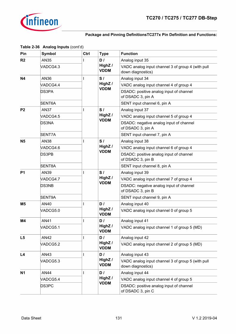
TC270 / TC275 / TC277 DB-Step
Package and Pinning DefinitionsTC277x Pin Definition and Functions:
Data Sheet 131 V 1.2 2019-04
R2 AN35 I D /HighZ /VDDM
Analog input 35VADCG4.3 VADC analog input channel 3 of group 4 (with pull
down diagnostics)N4 AN36 I S /
HighZ /VDDM
Analog input 34VADCG4.4 VADC analog input channel 4 of group 4DS3PA DSADC: positive analog input of channel
of DSADC 3, pin ASENT6A SENT input channel 6, pin A
P2 AN37 I S /HighZ /VDDM
Analog input 37VADCG4.5 VADC analog input channel 5 of group 4DS3NA DSADC: negative analog input of channel
of DSADC 3, pin ASENT7A SENT input channel 7, pin A
N5 AN38 I S /HighZ /VDDM
Analog input 38VADCG4.6 VADC analog input channel 6 of group 4DS3PB DSADC: positive analog input of channel
of DSADC 3, pin BSENT8A SENT input channel 8, pin A
P1 AN39 I S /HighZ /VDDM
Analog input 39VADCG4.7 VADC analog input channel 7 of group 4DS3NB DSADC: negative analog input of channel
of DSADC 3, pin BSENT9A SENT input channel 9, pin A
M5 AN40 I D /HighZ /VDDM
Analog input 40VADCG5.0 VADC analog input channel 0 of group 5
M4 AN41 I D /HighZ /VDDM
Analog input 41VADCG5.1 VADC analog input channel 1 of group 5 (MD)
L5 AN42 I D /HighZ /VDDM
Analog input 42VADCG5.2 VADC analog input channel 2 of group 5 (MD)
L4 AN43 I D /HighZ /VDDM
Analog input 43VADCG5.3 VADC analog input channel 3 of group 5 (with pull
down diagnostics)N1 AN44 I D /
HighZ /VDDM
Analog input 44VADCG5.4 VADC analog input channel 4 of group 5DS3PC DSADC: positive analog input of channel
of DSADC 3, pin C
Table 2-36 Analog Inputs (cont’d)Pin Symbol Ctrl Type Function

TC270 / TC275 / TC277 DB-Step
Package and Pinning DefinitionsTC277x Pin Definition and Functions:
Data Sheet 132 V 1.2 2019-04
N2 AN45 I D /HighZ /VDDM
Analog input 45VADCG5.5 VADC analog input channel 5 of group 5DS3NC DSADC: negative analog input of channel
of DSADC 3, pin CM1 AN46 I D /
HighZ /VDDM
Analog input 46VADCG5.6 VADC analog input channel 6 of group 5DS3PD DSADC: positive analog input of channel
of DSADC 3, pin DM2 AN47 I D /
HighZ /VDDM
Analog input 47VADCG5.7 VADC analog input channel 7 of group 5DS3ND DSADC: negative analog input of channel
of DSADC 3, pin D
Table 2-37 System I/OPin Symbol Ctrl Type FunctionG17 PORST I I /
PD /VEXT
Power On Reset InputAdditional strong PD in case of power fail.
F16 ESR0 I/O MP /OD /VEXT
External System Request Reset 0Default configuration during and after reset is open-drain driver. The driver drives low during power-on reset. This is valid additionally after deactivation of PORST until the internal reset phase has finished. See also SCU chapter for details.Default after power-on can be different. See also SCU chapter ´Reset Control Unit´ and SCU_IOCR register description.
EVRWUP I EVR Wakeup PinG16 ESR1 I/O MP / PU1 /
VEXTExternal System Request Reset 1Default NMI function. See also SCU chapter ´Reset Control Unit´ and SCU_IOCR register description.
EVRWUP I EVR Wakeup PinW17 VGATE1P O VGATE1P
/- /VEXT
External Pass Device gate control for EVR13
K16 TMS I A2 / PD /VDDP3
JTAG Module State Machine Control InputDAP1 I/O Device Access Port Line 1
L19 TRST I A2 / PD /VDDP3
JTAG Module Reset/Enable Input
Table 2-36 Analog Inputs (cont’d)Pin Symbol Ctrl Type Function

TC270 / TC275 / TC277 DB-Step
Package and Pinning DefinitionsTC277x Pin Definition and Functions:
Data Sheet 133 V 1.2 2019-04
J16 TCK I A2 / PD /VDDP3
JTAG Module Clock InputDAP0 I Device Access Port Line 0
M20 XTAL1 I XTAL1 /- /VDDP3
Main Oscillator/PLL/Clock Generator Input
M19 XTAL2 O XTAL2 /- /VDDP3
Main Oscillator/PLL/Clock Generator Output
Table 2-38 SupplyPin Symbol Ctrl Type FunctionY6 VAREF1 I Vx Positive Analog Reference Voltage 1
Y7 VAGND1 I Vx Negative Analog Reference Voltage 1
T1 VAREF2 I Vx Positive Analog Reference Voltage 2
T2 VAGND2 I Vx Negative Analog Reference Voltage 2
Y5 VDDM I Vx ADC Analog Power Supply (3.3V / 5V)
G8, H7 VDD / VDDSB I Vx Emulation Device: Emulation SRAM Standby Power Supply (1.3V) (Emulation Device only).Production Device: VDD (1.3V).
P8, P13, N7, N14, H14, G13
VDD I Vx Digital Core Power Supply (1.3V)
N19 VDD I Vx Digital Core Power Supply (1.3V).The supply pin inturn supplies the main XTAL Oscillator/PLL (1.3V) . A higher decoupling capacitor is therefore recommended to the VSS pin for better noise immunity.
A2, B3, V19, W20
VEXT I Vx External Power Supply (5V / 3.3V)
B18, A19 VDDP3 I Vx Digital Power Supply for Flash (3.3V).Can be also used as external 3.3V Power Supply for VFLEX.
N20 VDDP3 I Vx Digital Power Supply for Oscillator, LVDSH and A2 pads (3.3V).The supply pin inturn supplies the main XTAL Oscillator/PLL (3.3V) . A higher decoupling capacitor is therefore recommended to the VSS pin for better noise immunity.
Table 2-37 System I/O (cont’d)Pin Symbol Ctrl Type Function

TC270 / TC275 / TC277 DB-Step
Package and Pinning DefinitionsTC277x Pin Definition and Functions:
Data Sheet 134 V 1.2 2019-04
E15, D16 VDDFL3 I Vx Flash Power Supply (3.3V)
D5 VFLEX I Vx Digital Power Supply for Flex Port Pads(5V / 3.3V)
Y4 VSSM I Vx Analog Ground for VDDM
T11 VEVRSB I Vx Standby Power Supply (3.3V/5V) for the Standby SRAM (CPU0.DSPR). If Standby mode is not used: To be handled like VEXT (3.3V/5V).
B2, D4, E5, L20, T16, U17, W19, Y20
VSS I Vx Digital Ground
E16, D17, B19, A20
VSS I Vx Digital Ground (outer balls)
P9, P12, N9, N10, N11, N12
VSS I Vx Digital Ground (center balls)
M7, M8, M10, M11, M13, M14
VSS I Vx Digital Ground (center balls)
L8, L9, L10, L11, L12, L13
VSS I Vx Digital Ground (center balls)
K8, K9, K10, K11, K12, K13
VSS I Vx Digital Ground (center balls)
J7, J8, J10, J11, J13, J14
VSS I Vx Digital Ground (center balls)
H9, H10, H11, H12, G9, G10, G11, G12
VSS I Vx Digital Ground (center balls)
P10 VSS I Vx Digital Ground (center balls)This ball is used in the Emulation Device as AGBT TX0N
P11 VSS I Vx Digital Ground (center balls)This ball is used in the Emulation Device as AGBT TX0P
L7 VSS I Vx Digital Ground (center balls)This ball is used in the Emulation Device as AGBT CLKN
Table 2-38 Supply (cont’d)Pin Symbol Ctrl Type Function

TC270 / TC275 / TC277 DB-Step
Package and Pinning DefinitionsTC277x Pin Definition and Functions:
Data Sheet 135 V 1.2 2019-04
Legend:Column “Ctrl.”:I = Input (for GPIO port Lines with IOCR bit field Selection PCx = 0XXXB)O = OutputO0 = Output with IOCR bit field selection PCx = 1X000BO1 = Output with IOCR bit field selection PCx = 1X001B (ALT1)O2 = Output with IOCR bit field selection PCx = 1X010B (ALT2)O3 = Output with IOCR bit field selection PCx = 1X011B (ALT3)O4 = Output with IOCR bit field selection PCx = 1X100B (ALT4)O5 = Output with IOCR bit field selection PCx = 1X101B (ALT5)O6 = Output with IOCR bit field selection PCx = 1X110B (ALT6)O7 = Output with IOCR bit field selection PCx = 1X111B (ALT7)Column “Type”:LP = Pad class LP (5V/3.3V, LVTTL)MP = Pad class MP (5V/3.3V, LVTTL)MP+ = Pad class MP+ (5V/3.3V, LVTTL)MPR = Pad class MPR (5V/3.3V, LVTTL)A2 = Pad class A2 (3.3V, LVTTL)LVDSM = Pad class LVDSM (LVDS/CMOS 5V/3.3V)LVDSH = Pad class LVDSH (LVDS/CMOS 3.3V)S = Pad class S (ADC overlayed with General Purpose Input)D = Pad class D (ADC)PU = with pull-up device connected during reset (PORST = 0)PU1 = with pull-up device connected during reset (PORST = 0)1) 2) 3)
K7 VSS I Vx Digital Ground (center balls)This ball is used in the Emulation Device as AGBT CLKP
L14 VSS I Vx Digital Ground (center balls)This ball is used in the Emulation Device as AGBT ERR
K14 NC / VDDPSB I NCVDDPSB
Emulation Device: Power Supply (3.3V) for DAP/JTAG pad group. Can be connected to VDDP or can be left unsupplied (see document ́ AurixED´ / Aurix Emulation Devices specification).
Production Device: This pin is not connected on package level. It can be connected on PCB level to VDDP or Ground or can be left unsupplied.
A1, Y1, U4 NC I NC Not Connected. These pins are not connected on package level and will not be used for future extensions.
1) The default state of GPIOs (Px.y) during and after PORST active is controllled via HWCFG[6] (P14.4). HWCFG[6] has a weak internal pull-up active at start-up if the pin is left unconnected.See also User´s Manual, “Introduction Chapter”, “General Purpose I/O Ports and Peripheral I/O Lines”, Figure: “Default state of port pins during and after reset”.
Table 2-38 Supply (cont’d)Pin Symbol Ctrl Type Function
TC270 / TC275 / TC277 DB-Step
Package and Pinning DefinitionsTC277x Pin Definition and Functions:
Data Sheet 136 V 1.2 2019-04
PD = with pull-down device connected during reset (PORST = 0)PD1 = with pull-down device connected during reset (PORST = 0)1) 2) 3) PX = Behavior depends on usage: PD in EVR13 SMPS Mode and PU1 in GPIO ModeOD = open drain during reset (PORST = 0)HighZ = tri-state during reset (PORST = 0)PORST = PORST input padXTAL1 = XTAL1 input padXTAL2 = XTAL2 input padVGATE1P = VGATE1PVGATE3P = VGATE3PVx = SupplyNC = These pins are reserved for future extensions and shall not be connected externallyNC1 = These pins are not connected on package level and will not be used for future extensionsNCVDDPSB = This pin has a different functionality in an Production Device and an Emulation Device. For detailspls. see Pin/Ball description of this pin.NCVDDSB = This pin has a different functionality in an Production Device and an Emulation Device. For detailspls. see Pin/Ball description of this pin.
2.2.2 Emergency Stop FunctionThe Emergency Stop function can be used to force GPIOs (General Purpose Inputs/Outputs) via an external inputsignal (EMGSTOPA or EMGSTOPB) into a defined state:• Input state and• PU or High-Z depending on HWCFG[6] level latched during PORST activeControl of the Emergency Stop function:• The Emergency Stop function can be enabled/disabled in the SCU (see chapter “SCU”, “Emergency Stop
Control”)• The Emergency Stop input signal, EMGSTOPA (P33.8) / EMGSTOPB (P21.2) , can selected in the SCU (see
chapter “SCU”, “Emergency Stop Control”)• On port level, each GPIO can be enabled/disabled for the Emergency Stop function via the Px_ESR (Port x
Emergency Stop) registers in the port control logic (see chapter “General Purpose I/O Ports and Peripheral I/O Lines”, “Emergency Stop Register”).
The Emergency Stop function is available for all GPIO Ports with the following exceptions:• Not available for P20.2 (General Purpose Input/GPI only, overlayed with Testmode)• Not available for P40.x (analoge input ANx overlayed with GPI)• Not available for P32.0 EVR13 SMPS mode.• Not available for dedicated I/O without General Purpose Output function (e.g ESRx, TMS, TCK)The Emergency Stop function can be overruled on the following GPIO Ports:• P00.x: Emergency Stop can be overruled by the VADC. Overruling can be disabled via the control register
P00_SCR (see chapter “General Purpose I/O Ports and Peripheral I/O Lines”, P00)• P14.0 and P14.1: Emergency Stop can be overruled in the DXCPL mode (DAP over can physical layer mode).
No Overruling in the DXCM (Debug over can message) mode• P21.6: Emergency Stop can be overruled in JTAG mode if this pin is used as TDI• P21.7: Emergency Stop can be overruled in JTAG or Three Pin DAP mode
2) If HWCFG[6] is left unconnected or is externally pulled high, weak internal pull-ups (PU1) / pull-downs (PD1) are active during and after reset.
3) If HWCFG[6] is connected to ground, the PD1 / PU1 pins are predominantly in HighZ during and after reset.

TC270 / TC275 / TC277 DB-Step
Package and Pinning DefinitionsTC277x Pin Definition and Functions:
Data Sheet 137 V 1.2 2019-04
• P20.0: Emergency Stop can be overruled in JTAG mode if this GPIO is used as TDI
2.2.3 Pull-Up/Pull-Down Reset Behavior of the Pins
In case of leakage test (PORST = 0 and TESTMODE = 0), the pull-down of the TRST pin is switched off. In caseof an user application (TESTMODE = 1), the pull-down of the TRST is always switched on.
Table 2-39 List of Pull-Up/Pull-Down Reset Behavior of the PinsPins PORST = 0 PORST = 1all GPIOs Pull-up if HWCFG[6] = 1 or High-Z if HWCFG[6] = 0TDI, TESTMODE Pull-upPORST1)
1) Pull-down with IPORST relevant is always activated when a primary supply monitor detects a violation.
Pull-down with IPORST relevant Pull-down with IPDLI relevantTRST, TCK, TMS Pull-downESR0 The open-drain driver is used to
drive low.2)
2)Valid additionally after deactivation of PORST until the internal reset phase has finished. See the SCU chapter for details.
Pull-up3)
3) See the SCU_IOCR register description.
ESR1 Pull-up3)
TDO Pull-up High-Z/Pull-up4)
4) Depends on JTAG/DAP selection with TRST.

TC270 / TC275 / TC277 DB-Step
Package and Pinning DefinitionsTC270x Bare Die Pad Definition
Data Sheet 138 V 1.2 2019-04
2.3 TC270x Bare Die Pad Definition The TC270x Bare Die Logic Symbol is shown in Figure 2-3. Table 2-40 describes the pads of the TC270x Bare Die. It describes also the mapping of VADC / DS-ADCchannels to the analog inputs (ANx) and the mapping of Port functions to the pads. Note: The detailed description of the port functions (Px.y) can be found in the User’s Manual chapter “General
Purpose I/O Ports and Peripheral I/O LInes (Ports)“.
Figure 2-3 TC270x Logic Symbol for the Bare Die.
Table 2-40 List of the TC270x Bare Die PadsNumber Pad Name Pad Type X Y Comment1 P10.8 LP / PU1 / VEXT 3265500 -3460000 GPIO2 P02.0 MP+ / PU1 /
VEXT3374000 -3380000 GPIO
3 P02.9 LP / PU1 / VEXT 3265500 -3300000 GPIO4 P02.1 LP / PU1 / VEXT 3265500 -3200000 GPIO5 VSS Vx 3374000 -3125000 Must be bonded to VSS6 P02.10 LP / PU1 / VEXT 3265500 -3050000 GPIO7 P02.2 MP+ / PU1 /
VEXT3374000 -2950000 GPIO
8 P02.11 LP / PU1 / VEXT 3265500 -2850000 GPIO9 VEXT Vx 3374000 -2775000 Must be bonded to VEXT10 P02.3 LP / PU1 / VEXT 3265500 -2670000 GPIO
Pad 173
Pad 172
Pad 84
Pad 85
Pad 255
Pad 256 Pad 332
Pad 1
0.0X
Y

TC270 / TC275 / TC277 DB-Step
Package and Pinning DefinitionsTC270x Bare Die Pad Definition
Data Sheet 139 V 1.2 2019-04
11 P02.4 MP+ / PU1 / VEXT
3265500 -2540000 GPIO
12 VSS Vx 3374000 -2465000 Must be bonded to VSS13 P02.5 MP+ / PU1 /
VEXT3265500 -2390000 GPIO
14 P02.6 MP / PU1 / VEXT 3374000 -2300000 GPIO15 VEXT Vx 3374000 -2195000 Must be bonded to VEXT16 P02.7 MP / PU1 / VEXT 3265500 -2110000 GPIO17 P02.8 LP / PU1 / VEXT 3374000 -2040000 GPIO18 VSS Vx 3374000 -1940000 Must be bonded to VSS19 P01.3 LP / PU1 / VEXT 3265500 -1883500 GPIO20 VDD Vx 3374000 -1818500 Must be bonded to VDD21 VSS Vx 3374000 -1688500 Must be bonded to VSS22 VSS Vx 3374000 -1644500 Must be bonded to VSS.
Double Pad (Elephant Pad), shared with Pad Nr 22.
23 VDD Vx 3374000 -1514500 Must be bonded to VSS.Double Pad (Elephant Pad), shared with Pad Nr 21.
24 P01.4 LP / PU1 / VEXT 3265500 -1449500 GPIO25 VSS Vx 3374000 -1394500 Must be bonded to VSS26 P01.5 LP / PU1 / VEXT 3265500 -1339500 GPIO27 P01.6 LP / PU1 / VEXT 3265500 -1239500 GPIO28 P01.7 LP / PU1 / VEXT 3265500 -1139500 GPIO29 VEXT Vx 3374000 -1068500 Must be bonded to VEXT30 VSS Vx 3374000 -968500 Must be bonded to VSS31 P00.0 MP / PU1 / VEXT 3265500 -868500 GPIO32 P00.1 LP / PU1 / VEXT 3265500 -241000 GPIO33 P00.2 LP / PU1 / VEXT 3265500 -141000 GPIO34 P00.3 LP / PU1 / VEXT 3265500 -41000 GPIO35 VSS Vx 3374000 19000 Must be bonded to VSS36 P00.4 LP / PU1 / VEXT 3265500 79000 GPIO37 P00.5 LP / PU1 / VEXT 3265500 179000 GPIO38 P00.6 LP / PU1 / VEXT 3265500 279000 GPIO39 VEXT Vx 3374000 339000 Must be bonded to VEXT40 P00.7 LP / PU1 / VEXT 3265500 399000 GPIO41 P00.8 LP / PU1 / VEXT 3374000 459000 GPIO42 P00.9 LP / PU1 / VEXT 3265500 549000 GPIO
Table 2-40 List of the TC270x Bare Die PadsNumber Pad Name Pad Type X Y Comment

TC270 / TC275 / TC277 DB-Step
Package and Pinning DefinitionsTC270x Bare Die Pad Definition
Data Sheet 140 V 1.2 2019-04
43 P00.10 LP / PU1 / VEXT 3374000 609000 GPIO44 P00.11 LP / PU1 / VEXT 3265500 689000 GPIO45 VSS Vx 3374000 749000 Must be bonded to VSS46 P00.12 LP / PU1 / VEXT 3265500 809000 GPIO47 VDD Vx 3374000 864000 Must be bonded to VDD48 VSS Vx 3374000 964000 Must be bonded to VSS49 VSS Vx 3374000 1064000 Must be bonded to VSS50 VDD Vx 3374000 1164000 Must be bonded to VDD51 VEXT Vx 3265500 1239000 Must be bonded to VEXT52 VSS Vx 3374000 1299000 Must be bonded to VSS53 VAREF3 Vx 3374000 1419000 Positive Analog Reference
Voltage 354 VAREF2 Vx 3265500 1479000 Positive Analog Reference
Voltage 255 VAGND3 Vx 3374000 1539000 Negative Analog Reference
Voltage 356 VAGND2 Vx 3265500 1599000 Negative Analog Reference
Voltage 257 VDDM Vx 3374000 1659000 Must be bonded to VEXT58 AN47 (VADC5.7 /
DS3ND)D 3265500 1719000 Analog input
59 AN46 (VADC5.6 / DS3PD)
D 3374000 1779000 Analog input
60 AN45 (VADC5.5 / DS3NC)
D 3265500 1839000 Analog input
61 AN44 (VADC5.4 / DS3PC)
D 3374000 1899000 Analog input
62 AN43 (VADC5.3) D 3265500 1959000 Analog input (with pull down diagnostics)
63 AN42 (VADC5.2) D 3374000 2019000 Analog input64 AN41 (VADC5.1) D 3265500 2079000 Analog input65 AN40 (VADC5.0) D 3374000 2139000 Analog input66 AN39 (VADC4.7 /
DS3NB), P40.9 ( SENT9A)
S 3265500 2199000 Analog input, GPI (SENT)
67 AN38 (VADC4.6 / DS3PB), P40.8 ( SENT8A)
S 3374000 2259000 Analog input, GPI (SENT)
68 AN37 (VADC4.5 / DS3NA), P40.7 ( SENT7A)
S 3265500 2319000 Analog input, GPI (SENT)
Table 2-40 List of the TC270x Bare Die PadsNumber Pad Name Pad Type X Y Comment

TC270 / TC275 / TC277 DB-Step
Package and Pinning DefinitionsTC270x Bare Die Pad Definition
Data Sheet 141 V 1.2 2019-04
69 VDDM Vx 3374000 2379000 Must be bonded to VEXT70 AN36 (VADC4.4 /
DS3PA), P40.6 ( SENT6A)
S 3265500 2439000 Analog input, GPI (SENT)
71 VSSM Vx 3374000 2499000 Must be bonded to VSS72 AN35 (VADC4.3) D 3265500 2559000 Analog input (with pull
down diagnostics)73 AN34 (VADC4.2) D 3374000 2619000 Analog input74 AN33
(VADC4.1), P40.5 ( SENT5A)
S 3265500 2679000 Analog input, GPI (SENT)
75 AN32 (VADC4.0), P40.4 ( SENT4A)
S 3374000 2765000 Analog input, GPI (SENT)
76 AN31 (VADC3.7) D 3265500 2825000 Analog input77 AN30 (VADC3.6) D 3374000 2885000 Analog input78 AN29 (VADC3.5) D 3265500 2945000 Analog input79 AN28 (VADC3.4) D 3374000 3045000 GPIO80 AN27
(VADC3.3), P40.3 ( SENT3A)
S 3265500 3105000 Analog input (with pull down diagnostics), GPI (SENT)
81 AN26 (VADC3.2), P40.2 ( SENT2A)
S 3265500 3205000 Analog input, GPI (SENT)
82 AN25 (VADC3.1 / DS2NB), P40.1 ( SENT1A)
S 3265500 3305000 Analog input, GPI (SENT)
83 AN24 (VADC3.0 / DS2PB), P40.0 ( SENT0A)
S 3265500 3405000 Analog input, GPI (SENT)
84 VDDM Vx 3374000 3465000 Must be bonded to VEXT85 VSSM Vx 3134000 3705000 Must be bonded to VSS86 AN23 (VADC2.7) D 3074000 3596500 Analog input87 AN22 (VADC2.6) D 3014000 3705000 Analog input88 AN21 (VADC2.5 /
DS2NA)D 2954000 3596500 Analog input
89 AN20 (VADC2.4 / DS2PA)
D 2854000 3596500 Analog input
90 AN19 (VADC2.3) D 2754000 3596500 Analog input (with pull down diagnostics)
91 AN18 (VADC2.2) D 2654000 3596500 Analog input92 AN17 (VADC2.1) D 2554000 3596500 Analog input
Table 2-40 List of the TC270x Bare Die PadsNumber Pad Name Pad Type X Y Comment

TC270 / TC275 / TC277 DB-Step
Package and Pinning DefinitionsTC270x Bare Die Pad Definition
Data Sheet 142 V 1.2 2019-04
93 AN16 (VADC2.0) D 2494000 3705000 Analog input94 AN15 (VADC1.7) D 2434000 3596500 Analog input95 VAGND1 Vx 2374000 3705000 Negative Analog Reference
Voltage 196 VAGND0 Vx 2314000 3596500 Negative Analog Reference
Voltage 097 VAREF1 Vx 2254000 3705000 Positive Analog Reference
Voltage 198 VAREF0 Vx 2194000 3596500 Positive Analog Reference
Voltage 099 VSSM Vx 2134000 3705000 Must be bonded to VSS100 VSSM Vx 2074000 3596500 Must be bonded to VSS101 VSSMREF Vx 2014000 3705000 Must be bonded to VSS102 AN14 (VADC1.6) D 1954000 3596500 Analog input103 VDDM Vx 1894000 3705000 Must be bonded to VEXT104 VDDM Vx 1829000 3596500 Must be bonded to VEXT105 AN13 (VADC1.5) D 1724000 3596500 Analog input106 AN12 (VADC1.4) D 1664000 3705000 Analog input107 AN11 (VADC1.3) D 1604000 3596500 Analog input (with pull
down diagnostics)108 AN10 (VADC1.2) D 1544000 3705000 Analog input109 AN9 (VADC1.1) D 1484000 3569500 Analog input110 AN8 (VADC1.0) D 1424000 3705000 Analog input111 AN7 (VADC0.7) D 1364000 3596500 Analog input (with pull
down diagnostics)112 AN6 (VADC0.6) D 1304000 3705000 Analog input113 AN5 (VADC0.5) D 1244000 3596500 Analog input114 AN4 (VADC0.4) D 1184000 3705000 Analog input115 AN3 (VADC0.3 /
DS0NA)D 1124000 3596500 Analog input
116 VSSM Vx 1064000 3705000 Must be bonded to VSS117 AN2 (VADC0.2 /
DS0PA)D 1004000 3596500 Analog input
118 VDDM Vx 944000 3705000 Must be bonded to VEXT119 AN1 (VADC0.1 /
DS1NA)D 884000 3596500 Analog input
120 AN0 (VADC0.0 / DS1PA)
D 807000 3705000 Analog input
121 VEXT Vx 427000 3596500 Must be bonded to VEXT122 VSS Vx 377000 3705000 Must be bonded to VSS
Table 2-40 List of the TC270x Bare Die PadsNumber Pad Name Pad Type X Y Comment
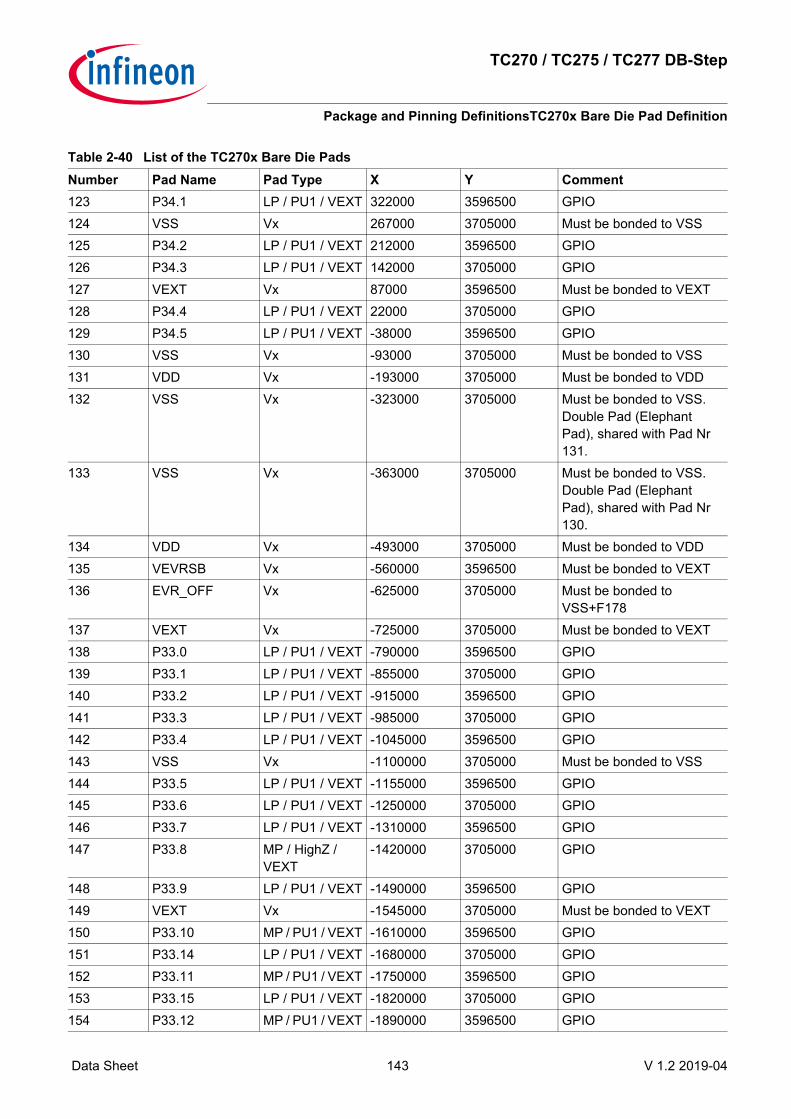
TC270 / TC275 / TC277 DB-Step
Package and Pinning DefinitionsTC270x Bare Die Pad Definition
Data Sheet 143 V 1.2 2019-04
123 P34.1 LP / PU1 / VEXT 322000 3596500 GPIO124 VSS Vx 267000 3705000 Must be bonded to VSS125 P34.2 LP / PU1 / VEXT 212000 3596500 GPIO126 P34.3 LP / PU1 / VEXT 142000 3705000 GPIO127 VEXT Vx 87000 3596500 Must be bonded to VEXT128 P34.4 LP / PU1 / VEXT 22000 3705000 GPIO129 P34.5 LP / PU1 / VEXT -38000 3596500 GPIO130 VSS Vx -93000 3705000 Must be bonded to VSS131 VDD Vx -193000 3705000 Must be bonded to VDD132 VSS Vx -323000 3705000 Must be bonded to VSS.
Double Pad (Elephant Pad), shared with Pad Nr 131.
133 VSS Vx -363000 3705000 Must be bonded to VSS.Double Pad (Elephant Pad), shared with Pad Nr 130.
134 VDD Vx -493000 3705000 Must be bonded to VDD135 VEVRSB Vx -560000 3596500 Must be bonded to VEXT136 EVR_OFF Vx -625000 3705000 Must be bonded to
VSS+F178137 VEXT Vx -725000 3705000 Must be bonded to VEXT138 P33.0 LP / PU1 / VEXT -790000 3596500 GPIO139 P33.1 LP / PU1 / VEXT -855000 3705000 GPIO140 P33.2 LP / PU1 / VEXT -915000 3596500 GPIO141 P33.3 LP / PU1 / VEXT -985000 3705000 GPIO142 P33.4 LP / PU1 / VEXT -1045000 3596500 GPIO143 VSS Vx -1100000 3705000 Must be bonded to VSS144 P33.5 LP / PU1 / VEXT -1155000 3596500 GPIO145 P33.6 LP / PU1 / VEXT -1250000 3705000 GPIO146 P33.7 LP / PU1 / VEXT -1310000 3596500 GPIO147 P33.8 MP / HighZ /
VEXT-1420000 3705000 GPIO
148 P33.9 LP / PU1 / VEXT -1490000 3596500 GPIO149 VEXT Vx -1545000 3705000 Must be bonded to VEXT150 P33.10 MP / PU1 / VEXT -1610000 3596500 GPIO151 P33.14 LP / PU1 / VEXT -1680000 3705000 GPIO152 P33.11 MP / PU1 / VEXT -1750000 3596500 GPIO153 P33.15 LP / PU1 / VEXT -1820000 3705000 GPIO154 P33.12 MP / PU1 / VEXT -1890000 3596500 GPIO
Table 2-40 List of the TC270x Bare Die PadsNumber Pad Name Pad Type X Y Comment

TC270 / TC275 / TC277 DB-Step
Package and Pinning DefinitionsTC270x Bare Die Pad Definition
Data Sheet 144 V 1.2 2019-04
155 VSS Vx -1955000 3705000 Must be bonded to VSS156 P33.13 MP / PU1 / VEXT -2040000 3596500 GPIO157 VSS Vx -2105000 3705000 Must be bonded to VSS158 VDD Vx -2205000 3705000 Must be bonded to VDD159 P32.0 LP / EVR13
SMPS -> PD, GPIO -> PU1 / VEXT
-2260000 3596500 GPIO
160 VGATE1N (SMPS)
VGATE1N -2315000 3705000 Must be bonded to VSS if EVR13 SMPS is not used. Must be bonded to NMOS gate if EVR13 SMPS used.
161 VGATE1P (SMPS)
VGATE1P -2365000 3596500 Must be bonded to VEXT if EVR13 SMPS is not used. Must be bonded to PMOS gate if EVR13 SMPS used.
162 VGATE3P (LDO) VGATE3P -2415000 3705000 Must be bonded to VSS163 VGATE1P (LDO) VGATE1P -2465000 3596500 Must be bonded to VSS if
no external P channel MOSFET used for EVR13 LDO generation. Must be bonded to external P channnel MOSFET if external LDO pass device used.
164 VEXT Vx -2515000 3705000 Must be bonded to VEXT165 P32.2 LP / PU1 / VEXT -2570000 3596500 GPIO166 P32.3 LP / PU1 / VEXT -2714000 3596500 GPIO167 P32.6 LP / PU1 / VEXT -2774000 3705000 GPIO168 P32.5 LP / PU1 / VEXT -2849000 3596500 GPIO169 VSS Vx -2904000 3705000 Must be bonded to VSS170 P32.4 MP+ / PU1 /
VEXT-2989000 3596500 GPIO
171 P32.7 LP / PU1 / VEXT -3069000 3705000 GPIO172 P23.0 LP / PU1 / VEXT -3129000 3596500 GPIO173 VSS Vx -3374000 3391000 Must be bonded to VSS174 P23.1 MP+ / PU1 /
VEXT-3265500 3316000 GPIO
175 P23.2 LP / PU1 / VEXT -3374000 3236000 GPIO176 P23.3 LP / PU1 / VEXT -3265500 3125000 GPIO177 P23.4 MP+ / PU1 /
VEXT-3374000 3045000 GPIO
Table 2-40 List of the TC270x Bare Die PadsNumber Pad Name Pad Type X Y Comment

TC270 / TC275 / TC277 DB-Step
Package and Pinning DefinitionsTC270x Bare Die Pad Definition
Data Sheet 145 V 1.2 2019-04
178 P23.6 LP / PU1 / VEXT -3265500 2965000 GPIO179 VEXT Vx -3374000 2910000 Must be bonded to VEXT180 P23.5 MP+ / PU1 /
VEXT-3265500 2835000 GPIO
181 P23.7 LP / PU1 / VEXT -3374000 2755000 GPIO182 P22.0 MP / LVDSM_N /
PU1 / VEXT-3265500 2685000 GPIO
183 P22.1 MP / LVDS_P / PU1 / VEXT
-3265500 2335000 GPIO
184 VSS Vx -3374000 2270000 Must be bonded to VSS185 P22.2 MP / LVDSM_N /
PU1 / VEXT-3265500 2205000 GPIO
186 P22.3 MP / LVDS_P / PU1 / VEXT
-3265500 1855000 GPIO
187 VEXT Vx -3374000 1790000 Must be bonded to VEXT188 VEXT Vx -3265500 1735000 Must be bonded to VEXT189 Reserved Vx -3374000 1680000 Must be bonded to VSS190 VDD Vx -3374000 1580000 Must be bonded to VDD191 VSS Vx -3374000 1480000 Must be bonded to VSS192 P22.4 LP / PU1 / VEXT -3265500 1425000 GPIO193 VSS Vx -3374000 1370000 Must be bonded to VSS194 VDD Vx -3374000 1270000 Must be bonded to VDD195 P22.5 LP / PU1 / VEXT -3265500 1215000 GPIO196 P22.6 LP / PU1 / VEXT -3374000 1155000 GPIO197 P22.7 LP / PU1 / VEXT -3265500 1095000 GPIO198 VSS Vx -3374000 1040000 Must be bonded to VSS199 VDD Vx -3374000 940000 Must be bonded to VDD200 P22.8 LP / PU1 / VEXT -3265500 885000 GPIO201 P22.9 LP / PU1 / VEXT -3374000 825000 GPIO202 P22.10 LP / PU1 / VEXT -3265500 765000 GPIO203 VSS Vx -3374000 710000 Must be bonded to VSS204 P22.11 LP / PU1 / VEXT -3265500 655000 GPIO205 VDDOSC Vx -3374000 520000 Must be bonded to VDD206 VSSOSC Vx -3374000 420000 Must be bonded to VSS207 XTAL1 XTAL1 -3265500 312500 Main Oscillator/PLL/Clock
Generator Input. Must be bonded to external quartz or resonator
Table 2-40 List of the TC270x Bare Die PadsNumber Pad Name Pad Type X Y Comment

TC270 / TC275 / TC277 DB-Step
Package and Pinning DefinitionsTC270x Bare Die Pad Definition
Data Sheet 146 V 1.2 2019-04
208 XTAL2 XTAL2 -3265500 212500 Main Oscillator/PLL/Clock Generator Input. Must be bonded to external quartz or resonator
209 VSSOSC3 Vx -3374000 105000 Must be bonded to VSS210 VDDOSC3 Vx -3265500 55000 Must be bonded to VDDP3211 VDDP3 Vx -3374000 -35000 Must be bonded to VDDP3212 VDDP3 Vx -3265500 -95000 Must be bonded to VDDP3213 VSS Vx -3374000 -145000 Must be bonded to VSS214 P21.0 A2 / PU1 /
VDDP3-3374000 -245000 GPIO
215 P21.1 A2 / PU1 / VDDP3
-3265500 -345000 GPIO
216 VSS Vx -3374000 -395000 Must be bonded to VSS217 P21.2 LVDSH_N / PU1
/ VDDP3-3265500 -457500 GPIO
218 P21.3 LVDSH_P / PU1 / VDDP3
-3265500 -557500 GPIO
219 VDDP3 Vx -3374000 -620000 Must be bonded to VDDP3220 P21.4 LVDSH_N / PU1
/ VDDP3-3265500 -694500 GPIO
221 P21.5 LVDSH_P / PU1 / VDDP3
-3265500 -845500 GPIO
222 VDD Vx -3374000 -920000 Must be bonded to VDD223 VSS Vx -3374000 -1020000 Must be bonded to VSS224 P21.6 A2 / PU / VDDP3 -3265500 -1070000 GPIO, TDI225 VDDP3 Vx -3374000 -1120000 Must be bonded to VDDP3226 VSS Vx -3374000 -1345000 Must be bonded to VSS227 TMS / DAP1 A2 / PD / VDDP3 -3265500 -1395000 JTAG Module State
Machine Control Input / Device Access Port Line 1
228 P21.7 A2 / PU / VDDP3 -3374000 -1445000 GPIO, TDO229 TRST (N) A2 / PU / VDDP3 -3265500 -1535000 JTAG Module
Reset/Enable Input230 TCK / DAP0 A2 / PU / VDDP3 -3374000 -1585000 JTAG Module Clock Input /
Device Access Port Line 0231 P20.0 MP / PU1 / VEXT -3265500 -1720000 GPIO232 P20.1 LP / PU1 / VEXT -3374000 -1790000 GPIO233 P20.2 LP / PU / VEXT -3265500 -1845000 Testmode pin must be
bonded234 VSS Vx -3374000 -1895000 Must be bonded to VSS
Table 2-40 List of the TC270x Bare Die PadsNumber Pad Name Pad Type X Y Comment

TC270 / TC275 / TC277 DB-Step
Package and Pinning DefinitionsTC270x Bare Die Pad Definition
Data Sheet 147 V 1.2 2019-04
235 P20.3 LP / PU1 / VEXT -3265500 -1950000 GPIO236 ESR1 (N) /
EVRWUPMP / PU1 / VEXT -3374000 -2020000 External System Request
Reset 1. Default NMI function. EVR Wakeup Pin.
237 PORST (N) I / PD1 / VEXT -3265500 -2102500 Power On Reset Input. Additional strong PD in case of power fail.
238 VEXT Vx -3374000 -2170000 Must be bonded to VEXT239 ESR0 (N) /
EVRWUPMP / OD -3265500 -2235000 External System Request
Reset 0. Default configuration during and after reset is open-drain driver. The driver drives low during power-on reset. EVR Wakeup Pin.
240 VDD Vx -3374000 -2310000 Must be bonded to VDD241 VSS Vx -3374000 -2440000 Must be bonded to VSS.
Double Pad (Elephant Pad), shared with Pad Nr 240.
242 VSS Vx -3374000 -2480000 Must be bonded to VSS.Double Pad (Elephant Pad), shared with Pad Nr 239.
243 VDD Vx -3374000 -2610000 Must be bonded to VDD244 P20.6 LP / PU1 / VEXT -3265500 -2665000 GPIO245 VSS Vx -3374000 -2720000 Must be bonded to VSS246 P20.7 LP / PU1 / VEXT -3265500 -2775000 GPIO247 P20.8 MP / PU1 / VEXT -3374000 -2865000 GPIO248 P20.9 LP / PU1 / VEXT -3265500 -2935000 GPIO249 VEXT Vx -3374000 -2990000 Must be bonded to VEXT250 P20.10 MP / PU1 / VEXT -3265500 -3055000 GPIO251 P20.11 MP / PU1 / VEXT -3374000 -3155000 GPIO252 P20.12 MP / PU1 / VEXT -3265500 -3235000 GPIO253 VSS Vx -3374000 -3300000 Must be bonded to VSS254 P20.13 MP / PU1 / VEXT -3265500 -3365000 GPIO255 P20.14 MP / PU1 / VEXT -3265500 -3465000 GPIO256 P15.0 LP / PU1 / VEXT -3134000 -3596500 GPIO257 P15.1 LP / PU1 / VEXT -3034000 -3596500 GPIO258 P15.2 MP / PU1 / VEXT -2964000 -3705000 GPIO259 P15.3 MP / PU1 / VEXT -2864000 -3705000 GPIO260 VEXT Vx -2799000 -3596500 Must be bonded to VEXT
Table 2-40 List of the TC270x Bare Die PadsNumber Pad Name Pad Type X Y Comment
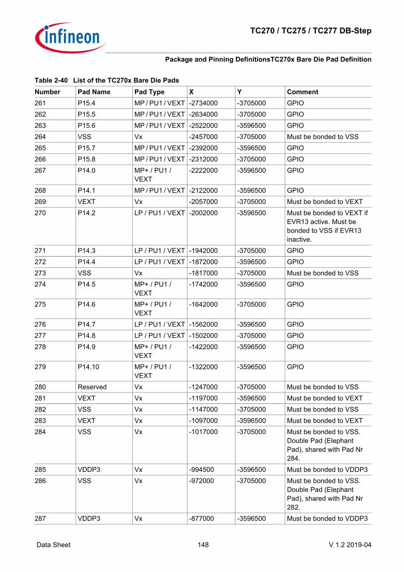
TC270 / TC275 / TC277 DB-Step
Package and Pinning DefinitionsTC270x Bare Die Pad Definition
Data Sheet 148 V 1.2 2019-04
261 P15.4 MP / PU1 / VEXT -2734000 -3705000 GPIO262 P15.5 MP / PU1 / VEXT -2634000 -3705000 GPIO263 P15.6 MP / PU1 / VEXT -2522000 -3596500 GPIO264 VSS Vx -2457000 -3705000 Must be bonded to VSS265 P15.7 MP / PU1 / VEXT -2392000 -3596500 GPIO266 P15.8 MP / PU1 / VEXT -2312000 -3705000 GPIO267 P14.0 MP+ / PU1 /
VEXT-2222000 -3596500 GPIO
268 P14.1 MP / PU1 / VEXT -2122000 -3596500 GPIO269 VEXT Vx -2057000 -3705000 Must be bonded to VEXT270 P14.2 LP / PU1 / VEXT -2002000 -3596500 Must be bonded to VEXT if
EVR13 active. Must be bonded to VSS if EVR13 inactive.
271 P14.3 LP / PU1 / VEXT -1942000 -3705000 GPIO272 P14.4 LP / PU1 / VEXT -1872000 -3596500 GPIO273 VSS Vx -1817000 -3705000 Must be bonded to VSS274 P14.5 MP+ / PU1 /
VEXT-1742000 -3596500 GPIO
275 P14.6 MP+ / PU1 / VEXT
-1642000 -3705000 GPIO
276 P14.7 LP / PU1 / VEXT -1562000 -3596500 GPIO277 P14.8 LP / PU1 / VEXT -1502000 -3705000 GPIO278 P14.9 MP+ / PU1 /
VEXT-1422000 -3596500 GPIO
279 P14.10 MP+ / PU1 / VEXT
-1322000 -3596500 GPIO
280 Reserved Vx -1247000 -3705000 Must be bonded to VSS281 VEXT Vx -1197000 -3596500 Must be bonded to VEXT282 VSS Vx -1147000 -3705000 Must be bonded to VSS283 VEXT Vx -1097000 -3596500 Must be bonded to VEXT284 VSS Vx -1017000 -3705000 Must be bonded to VSS.
Double Pad (Elephant Pad), shared with Pad Nr 284.
285 VDDP3 Vx -994500 -3596500 Must be bonded to VDDP3286 VSS Vx -972000 -3705000 Must be bonded to VSS.
Double Pad (Elephant Pad), shared with Pad Nr 282.
287 VDDP3 Vx -877000 -3596500 Must be bonded to VDDP3
Table 2-40 List of the TC270x Bare Die PadsNumber Pad Name Pad Type X Y Comment

TC270 / TC275 / TC277 DB-Step
Package and Pinning DefinitionsTC270x Bare Die Pad Definition
Data Sheet 149 V 1.2 2019-04
288 VDDFL3 Vx -777000 -3596500 Must be bonded to VDDP3289 VDDFL3 Vx -697000 -3705000 Must be bonded to VDDP3290 VDDFL3 Vx -629500 -3596500 Must be bonded to VDDP3291 VSS Vx -577000 -3705000 Must be bonded to VSS292 P13.0 MP / LVDSM_N /
PU1 / VEXT-512000 -3596500 GPIO
293 P13.1 MP / LVDS_P / PU1 / VEXT
-162000 -3596500 GPIO
294 VEXT Vx -97000 -3705000 Must be bonded to VEXT295 P13.2 MP / LVDSM_N /
PU1 / VEXT-32000 -3596500 GPIO
296 P13.3 MP / LVDS_P / PU1 / VEXT
318000 -3596500 GPIO
297 P12.0 LP / PU1 / VFLEX
458000 -3596500 GPIO
298 P12.1 LP / PU1 / VFLEX
518000 -3705000 GPIO
299 P11.0 MP+ / PU1 / VFLEX
598000 -3596500 GPIO
300 VSSFLEX Vx 673000 -3705000 Must be bonded to VSS301 P11.1 MP+ / PU1 /
VFLEX748000 -3596500 GPIO
302 VFLEX Vx 823000 -3705000 Must be bonded to VEXT or VDDP3
303 P11.2 MPR / PU1 / VFLEX
898000 -3596500 GPIO
304 P11.3 MPR / PU1 / VFLEX
998000 -3596500 GPIO
305 P11.4 MP+ / PU1 / VFLEX
1098000 -3705000 GPIO
306 P11.5 LP / PU1 / VFLEX
1178000 -3596500 GPIO
307 P11.6 MPR / PU1 / VFLEX
1258000 -3705000 GPIO
308 P11.7 LP / PU1 / VFLEX
1338000 -3596500 GPIO
309 P11.9 MP+ / PU1 / VFLEX
1418000 -3705000 GPIO
310 P11.8 LP / PU1 / VFLEX
1498000 -3596500 GPIO
311 VSSFLEX Vx 1553000 -3705000 Must be bonded to VSS
Table 2-40 List of the TC270x Bare Die PadsNumber Pad Name Pad Type X Y Comment

TC270 / TC275 / TC277 DB-Step
Package and Pinning DefinitionsTC270x Bare Die Pad Definition
Data Sheet 150 V 1.2 2019-04
Legend:Column “Number”:Running number of pads in the pad frameColumn “Name”:Symbolic name of the pad. The functions mapped on GPIO pads “Px.y” are described in the User’s Manual chapter ”General Purpose I/OPorts and Peripheral I/O LInes (Ports)”Column “Type”:LP = Pad class LP (5V/3.3V, LVTTL)MP = Pad class MP (5V/3.3V, LVTTL)MP+ = Pad class MP+ (5V/3.3V, LVTTL)
312 VFLEX Vx 1603000 -3596500 Must be bonded to VEXT or VDDP3
313 P11.10 LP / PU1 / VFLEX
1698000 -3705000 GPIO
314 P11.13 LP / PU1 / VFLEX
1758000 -3596500 GPIO
315 VSSFLEX Vx 1813000 -3705000 Must be bonded to VSS316 P11.11 MP+ / PU1 /
VFLEX1888000 -3596500 GPIO
317 P11.12 MPR / PU1 / VFLEX
1988000 -3596500 GPIO
318 P11.14 LP / PU1 / VFLEX
2068000 -3705000 GPIO
319 P11.15 LP / PU1 / VFLEX
2128000 -3596500 GPIO
320 VDD Vx 2183000 -3705000 Must be bonded to VDD321 VSS Vx 2283000 -3705000 Must be bonded to VSS322 VSS Vx 2403000 -3705000 Must be bonded to VSS323 P10.0 LP / PU1 / VEXT 2458000 -3596500 GPIO324 P10.1 MP+ / PU1 /
VEXT2543000 -3705000 GPIO
325 P10.2 MP / PU1 / VEXT 2643000 -3705000 GPIO326 P10.3 MP / PU1 / VEXT 2723000 -3596500 GPIO327 P10.4 MP+ / PU1 /
VEXT2834000 -3705000 GPIO
328 VEXT Vx 2909000 -3596500 Must be bonded to VEXT329 P10.5 LP / PU1 / VEXT 2964000 -3705000 GPIO330 P10.6 LP / PU1 / VEXT 3024000 -3596500 GPIO331 VSS Vx 3079000 -3705000 Must be bonded to VSS332 P10.7 LP / PU1 / VEXT 3134000 -3596500 GPIO
Table 2-40 List of the TC270x Bare Die PadsNumber Pad Name Pad Type X Y Comment

TC270 / TC275 / TC277 DB-Step
Package and Pinning DefinitionsTC270x Bare Die Pad Definition
Data Sheet 151 V 1.2 2019-04
MPR = Pad class MPR (5V/3.3V, LVTTL)A2 = Pad class A2 (3.3V, LVTTL)LVDSM = Pad class LVDSM (LVDS/CMOS 5V/3.3V)LVDSH = Pad class LVDSH (LVDS/CMOS 3.3V)S = Pad class S (ADC overlayed with General Purpose Input)D = Pad class D (ADC)PU = with pull-up device connected during reset (PORST = 0)PU1 = with pull-up device connected during reset (PORST = 0)1) 2) 3)
PD = with pull-down device connected during reset (PORST = 0)PD1 = with pull-down device connected during reset (PORST = 0)1) 2) 3) PX = Behavior depends on usage: PD in EVR13 SMPS Mode and PU1 in GPIO ModeOD = open drain during reset (PORST = 0)HighZ = tri-state during reset (PORST = 0)PORST = PORST input padXTAL1 = XTAL1 input padXTAL2 = XTAL2 input padVGATE1P = VGATE1PVGATE3P = VGATE3PVx = SupplyNC = These pins are reserved for future extensions and shall not be connected externallyNC1 = These pins are not connected on package level and will not be used for future extensionsNCVDDPSB = This pin has a different functionality in an Production Device and an Emulation Device. For detailspls. see Pin/Ball description of this pin.NCVDDSB = This pin has a different functionality in an Production Device and an Emulation Device. For detailspls. see Pin/Ball description of this pin.Column “X” / “Y”:Pad opening center coordinates (in nm)
2.3.1 Pad OpeningsTwo different pad openings are used:• Standard Pad Opening is 70um x 75um where 70um is the width of the opening (width as seen from the die
side) and 75um is the depth of the opening (from the die side into the silicon). • Double Pad or Elephant Pad Opening is 130um x 75um where 130um is the width of the opening (width as
seen from the die side) and 75um is the depth of the opening (from the die side into the silicon). The Double Pad openings are represented with two opening coordinates and two pad numbers. Double Pads are used only for supply and can be identified by the words ´Double Pad´ or ´Elephant Pad´ in the Comment column.
2.3.2 Emergency Stop FunctionThe Emergency Stop function can be used to force GPIOs (General Purpose Inputs/Outputs) via an external inputsignal (EMGSTOPA or EMGSTOPB) into a defined state:
1)The default state of GPIOs (Px.y) during and after PORST active is controllled via HWCFG[6] (P14.4). HWCFG[6] has a weakinternal pull-up active at start-up if the pin is left unconnected.See also User´s Manual, “Introduction Chapter”, “GeneralPurpose I/O Ports and Peripheral I/O Lines”, Figure: “Default state of port pins during and after reset”.2) If HWCFG[6] is left unconnected or is externally pulled high, weak internal pull-ups are active at GPIOs (Px.y) pins during
and after reset. Exceptions are P33.8 (HighZ), P40.x (default configuration during and after reset: analog inputs, port input funtion disabled), ESR0, P21.6 / P21.7 (port pins overlayed with JTAG functionality).
3) If HWCFG[6] is connected to ground, port pins are predominantly in HighZ during and after reset. Exceptions are P33.8 (HighZ), P40.x (default configuration during and after reset: analog inputs, port input funtion disabled), ESR0, P21.6 / P21.7 (port pins overlayed with JTAG functionality).

TC270 / TC275 / TC277 DB-Step
Package and Pinning DefinitionsTC270x Bare Die Pad Definition
Data Sheet 152 V 1.2 2019-04
• Input state and• PU or HighZ depending on HWCFG[6] level latched during PORST activeControl of the Emergency Stop function:• The Emergency Stop function can be enabled/disabled in the SCU (see chapter “SCU”, “Emergency Stop
Control”)• The Emergency Stop input signal, EMGSTOPA (P33.8) / EMGSTOPB (P21.2) , can selected in the SCU (see
chapter “SCU”, “Emergency Stop Control”)• On port level, each GPIO can be enabled/disabled for the Emergency Stop function via the Px_ESR (Port x
Emergency Stop) registers in the port control logic (see chapter “General Purpose I/O Ports and Peripheral I/O Lines”, “Emergency Stop Register”).
The Emergency Stop function is available for all GPIO Ports with the following exceptions:• Not available for P20.2 (General Purpose Input/GPI only, overlayed with Testmode)• Not available for P40.x (analoge input ANx overlayed with GPI)• Not available for P32.0 EVR13 SMPS mode.• Not available for dedicated I/O without General Purpose Output function (e.g ESRx, TMS, TCK)The Emergency Stop function can be overruled on the following GPIO Ports:• P00.x: Emergency Stop can be overruled by the VADC. Overruling can be disabled via the control register
P00_SCR (see chapter “General Purpose I/O Ports and Peripheral I/O Lines”, P00)• P14.0 and P14.1: Emergency Stop can be overruled in the DXCPL mode (DAP over can physical layer mode).
No Overruling in the DXCM (Debug over can message) mode• P21.6: Emergency Stop can be overruled in JTAG mode if this pin is used as TDI• P21.7: Emergency Stop can be overruled in JTAG or Three Pin DAP mode• P20.0: Emergency Stop can be overruled in JTAG mode if this GPIO is used as TDI
2.3.3 Pull-Up/Pull-Down Reset Behavior of the Pins
• In case of leakage test (PORST = 0 and TESTMODE = 0), the pull-down of the TRST pin is switched off. In case of an user application (TESTMODE = 1), the pull-down of the TRST is always switched on.
Table 2-41 List of Pull-Up/Pull-Down Reset Behavior of the PinsPins PORST = 0 PORST = 1all GPIOs Pull-up if HWCFG[6] = 1 or High-Z if HWCFG[6] = 0TDI, TESTMODE Pull-upPORST1)
1) Pull-down with IPORST relevant is always activated when a primary supply monitor detects a violation.
Pull-down with IPORST relevant Pull-down with IPDLI relevantTRST, TCK, TMS Pull-downESR0 The open-drain driver is used to
drive low.2)
2) Valid additionally after deactivation of PORST until the internal reset phase has finished. See the SCU chapter for details.
Pull-up3)
3) See the SCU_IOCR register description.
ESR1 Pull-up3)
TDO Pull-up High-Z/Pull-up4)
4) Depends on JTAG/DAP selection with TRST.

TC270 / TC275 / TC277 DB-Step
Electrical SpecificationParameter Interpretation
Data Sheet 153 V 1.2 2019-04
3 Electrical Specification
3.1 Parameter InterpretationThe parameters listed in this section partly represent the characteristics of the TC270 / TC275 / TC277 and partlyits requirements on the system. To aid interpreting the parameters easily when evaluating them for a design, theyare marked with an two-letter abbreviation in column “Symbol”:• CC
Such parameters indicate Controller Characteristics which are a distinctive feature of the TC270 / TC275 / TC277 and must be regarded for a system design.
• SRSuch parameters indicate System Requirements which must provided by the microcontroller system in which the TC270 / TC275 / TC277 designed in.

TC270 / TC275 / TC277 DB-Step
Electrical SpecificationAbsolute Maximum Ratings
Data Sheet 154 V 1.2 2019-04
3.2 Absolute Maximum RatingsStresses above the values listed under “Absolute Maximum Ratings” may cause permanent damage to the device.This is a stress rating only and functional operation of the device at these or any other conditions above thoseindicated in the Operational Conditions of this specification is not implied. Exposure to absolute maximum ratingconditions may affect device reliability.
Table 3-1 Absolute Maximum RatingsParameter Symbol Values Unit Note / Test Condition
Min. Typ. Max.Storage Temperature TST SR -65 - 170 °C upto 65h @ TJ =
150°C; upto 15h @ TJ = 170°C
Voltage at VDD power supply pins with respect to VSS 1)
1) Valid for cumulated for up to 2.8h and pulse forms following a power supply switch on phase, where the rise and fall times are releated to the system capacities and coils.
VDD SR - - 1.9 V
Voltage at VDDP3 and VDDFL3 power supply pins with respect to VSS 1)
VDDP3 SR - - 4.43 V
Voltage at VDDM, VEXT and VFLEX power supply pins with respect to VSS 1)
VDDM SR - - 7.0 V
Voltage on any class A2 and LVDSH input pin with respect to VSS 1)2)
2) Voltages below VINmin have no Impact to the device reliabiltiy as Long as the times and currents defined in section Pin Reliability in Overload for the affected pad(s) are not violated.
VIN SR -0.5 - min( VDDP3 + 0.6 , 4.23 )
V Whatever is lower
Voltage on all other input pins with respect to VSS 1)2)
VIN SR -0.5 - 7.0 V
Input current on any pin during overload condition 3)
3) This parameter is an Absolute Maximum Rating. Exposure to Absolute Maximum Ratings for extended periods of time may damage the device.
IIN SR -10 - 10 mA
Absolute maximum sum of all input circuit currents during overload condition 3)
ΣIIN SR -100 - 100 mA

TC270 / TC275 / TC277 DB-Step
Electrical SpecificationPin Reliability in Overload
Data Sheet 155 V 1.2 2019-04
3.3 Pin Reliability in OverloadWhen receiving signals from higher voltage devices, low-voltage devices experience overload currents andvoltages that go beyond their own IO power supplies specification.The following table defines overload conditions that will not cause any negative reliability impact if all the followingconditions are met:• full operation life-time is not exceeded• Operating Conditions are met for
– pad supply levels– temperature
If a pin current is out of the Operating Conditions but within the overload parameters, then the parametersfunctionality of this pin as stated in the Operating Conditions can no longer be guaranteed. Operation is stillpossible in most cases but with relaxed parameters.Note: An overload condition on one or more pins does not require a reset.
Table 3-2 Overload ParametersParameter Symbol Values Unit Note / Test Condition
Min. Typ. Max.Input current on any digital pin during overload condition
IIN -5 - 5 mA except LVDS pins-15 1) - 15 1) mA except LVDS pins;
limited to max. 20 pulses with 1ms pulse length
Input current on LVDS pin during overload condition
IINLVDS -3 - 3 mA
Absolute maximum sum of all input circuit currents during overload condition
IING -50 - 50 mA
Input current on analog input pin during overload condition
IINANA -3 - 3 mA-5 - 5 mA limited to 60h over
lifetimeAbsolute sum of all ADC inputs during overload condition
IINSCA -20 - 20 mA
Absolute maximum sum of all input circuit currents during overload condition
ΣIINS -100 - 100 mA
Signal voltage over/undershoot at GPIOs
VOUS VSS - 2 - VEXT/FLEX + 2
V limited to 60h over lifetime; Valid for LP, MP, MP+, and MPR pads
Inactive device pin current during overload condtion 2)
IID -1 - 1 mA All power supply voltages VDDx = 0
Sum of all inactive device pin currents 2)
IIDS -100 - 100 mA

TC270 / TC275 / TC277 DB-Step
Electrical SpecificationPin Reliability in Overload
Data Sheet 156 V 1.2 2019-04
Overload coupling factor for digital inputs, negative 3)
KOVDN CC - 2*10-4 6*10-4 Overload injected on GPIO non LVDS pad and affecting neighbor LP and A2 pads; -2mA < IIN < 0mA
- - 1*10-2 Overload injected on GPIO non LVDS pad and affecting neighbor LP and A2 pads; -5mA < IIN < -2mA
- - 1.7*10-3 Overload injected on GPIO non LVDS pad and affecting neighbor MP, MP+, and MPR pads; -2mA < IIN < 0mA
- - 2*10-2 Overload injected on GPIO non LVDS pad and affecting neighbor MP, MP+, and MPR pads; -5mA < IIN < -2mA
- - 0.3 Overload injected on LVDS pad and affecting neighbor LVDS pads
- - 0.93 coupling between pads 21.2 and 21.3
Overload coupling factor for digital inputs, positive 3)
KOVDP CC - - 1*10-5 Overload injected on GPIO non LVDS pad and affecting neighbor GPIO non LVDS pads
- - 1*10-4 Overload injected on GPIO pad and affecting neighbor P32.0 pad
- - 5*10-4 Overload injected on LVDS pad and affecting neighbor LVDS pads
Table 3-2 Overload Parameters (cont’d)Parameter Symbol Values Unit Note / Test Condition
Min. Typ. Max.

TC270 / TC275 / TC277 DB-Step
Electrical SpecificationPin Reliability in Overload
Data Sheet 157 V 1.2 2019-04
Note: DSADC input pins count as analog pins as they are overlaid with VADC pins.
Overload coupling factor for analog inputs, negative
KOVAN CC - - 6*10-4 4) Analog Inputs overlaid with class LP pads or pull down diagnostics; -1mA < IIN < 0mA
- - 1*10-2 Analog Inputs overlaid with class LP pads or pull down diagnostics; -5mA < IIN < -1mA
- - 1*10-4 else; -5mA < IIN < 0mAOverload coupling factor for analog inputs, positive
KOVAP CC - - 1*10-5 5mA < IIN < 0mA
1) Reduced VADC / DSADC result accuracy and / or GPIO input levels (VIL and VIH) can differ from specified parameters.2) Limitations for time and supply levels specified in this section are not valid for this parameter.3) Overload is measured as increase of pad leakage caused by injection on neighbor pad.4) For analogue inputs overlaid with DSADC function the VCM holdbuffer shall be enabled, in case DSADCs are enabled.
Table 3-3 PN-Junction Characteristics for positive OverloadPad Type IIN = 3 mA IIN = 5 mAF / A2 UIN = VDDP3 + 0.5 V UIN = VDDP3 + 0.6 VLP / MP / MP+ / MPR UIN = VEXT / FLEX + 0.75 V UIN = VEXT / FLEX + 0.8 VLVDSM UIN = VEXT + 0.75 V -LVDSH UIN = VDDP3 + 0.5 V -D UIN = VDDM + 0.75 V -
Table 3-4 PN-Junction Characteristics for negative OverloadPad Type IIN = -3 mA IIN = -5 mAF / A2 UIN = VSS - 0.5 V UIN = VSS - 0.6 VLP / MP / MP+ / MPR UIN = VSS - 0.75 V UIN = VSS - 0.8 VLVDSM UIN = VSS - 0.75 V -LVDSH UIN = VSS - 0.5 V -D UIN = VSS - 0.75 V -
Table 3-2 Overload Parameters (cont’d)Parameter Symbol Values Unit Note / Test Condition
Min. Typ. Max.

TC270 / TC275 / TC277 DB-Step
Electrical SpecificationOperating Conditions
Data Sheet 158 V 1.2 2019-04
3.4 Operating ConditionsThe following operating conditions must not be exceeded in order to ensure correct operation and reliability of theTC270 / TC275 / TC277. All parameters specified in the following tables refer to these operating conditions, unlessotherwise noticed.Digital supply voltages applied to the TC270 / TC275 / TC277 must be static regulated voltages.All parameters specified in the following tables refer to these operating conditions (see table below), unlessotherwise noticed in the Note / Test Condition column.
Table 3-5 Operating ConditionsParameter Symbol Values Unit Note / Test Condition
Min. Typ. Max.SRI frequency fSRI SR - - 200 MHzMax System Frequency fMAX SR - - 200 MHzCPU0 Frequency fCPU0 SR - - 200 MHzCPU1 Frequency fCPU1 SR - - 200 MHzCPU2 Frequency fCPU2 SR - - 200 MHzPLL output frequency fPLL SR 20 - 200 MHzPLL_ERAY output frequency fPLLERAY SR 20 - 400 MHzSPB frequency fSPB SR - - 100 MHzASCLIN fast frequency fASCLINF SR - - 200 MHzASCLIN slow frequency fASCLINS SR - - 100 MHzBaud2 frequency fBAUD2 SR - - 200 MHzBaud1 frequency fBAUD1 SR - - 100 MHzFSI2 frequency fFSI2 SR - - 200 MHzFSI frequency fFSI SR - - 100 MHzGTM frequency fGTM SR - - 100 MHzSTM frequency fSTM SR - - 100 MHzERAY frequency fERAY SR - - 80 MHzBBB frequency fBBB SR - - 100 MHzMultiCAN frequency fCAN SR - - 100 MHzAbsolute sum of short circuit currents of the device
ΣISC_D SR - - 100 mA
Ambient Temperature TA SR -40 - 125 °C valid for all SAK products
-40 - 150 °C valid for all SAL products
-40 - 170 °C valid for all SAL products without package
Junction Temperature TJ SR -40 - 150 °C valid for all SAK products
-40 - 170 °C valid for all SAL products

TC270 / TC275 / TC277 DB-Step
Electrical SpecificationOperating Conditions
Data Sheet 159 V 1.2 2019-04
Core Supply Voltage 1) VDD SR 1.17 1.3 1.43 2) V Only required if externally supplied
ADC analog supply voltage VDDM SR 2.97 5.0 5.5 3) VDigital external supply voltage for LP, MP, MP+ and LVDSM pads and EVR 4)
VEXT SR 2.97 - 4.5 V 3.3V pad parameters are valid
4.5 5.0 5.5 3) V 5V pad parameters are valid
Digital supply voltage for Flex port
VFLEX SR 2.97 - 4.5 V 3.3V pad parameters are valid
4.5 5.0 5.5 3) V 5V pad parameters are valid
Digital supply voltage for LVDSH and A2 pads 5)
VDDP3 SR 2.97 3.3 3.63 6) V 3.3V pad parameters are valid; only required if externally supplied
Flash supply voltage 3.3V 1) VDDFL3 SR 2.97 3.3 3.63 V Only required if externally supplied
Digital ground voltage VSS SR 0 - - VAnalog ground voltage for VDDM VSSM CC -0.1 0 0.1 VVoltage to ensure defined pad states 7)
VDDPPA CC 0.72 - - V A2 and LVDSH1.4 - - V LP, MP, MP+, MPR
and LVDSMDigital external supply voltage for EVR and during Standby mode
VEVRSB SR 2.97 - 5.5 V only available in BGA package. VEVRSB is bonded together with VEXT supply pin in LQFP package.
1) No external inductive load permissible if EVR is used. All VDD pins shall be connected together externally on the PCB.2) Voltage overshoot to 1.69V is permissible, provided the duration is less than 2h cumulated. Reduced ADC accuracy and
leakage is increased.3) Voltage overshoot to 6.5V is permissible, provided the duration is less than 2h cumulated. Reduced ADC accuracy and
leakage is increased. 4) All VEXT pins shall be connected together externally on the PCB.5) All VDDP3 pins shall be connected together externally on the PCB.6) Voltage overshoot to 4.29V is permissible, provided the duration is less than 2h cumulated. Reduced ADC accuracy and
leakage is increased.7) This parameter is valid under the assumption the PORST signal is constantly at low level during the power-up/power-down
of VDDP3.
Table 3-5 Operating Conditions (cont’d)Parameter Symbol Values Unit Note / Test Condition
Min. Typ. Max.

TC270 / TC275 / TC277 DB-Step
Electrical Specification5 V / 3.3 V switchable Pads
Data Sheet 160 V 1.2 2019-04
3.5 5 V / 3.3 V switchable PadsPad classes LP, MP, MP+, and MPR support both Automotive Level (AL) or TTL level (TTL) operation. Parametersare defined for AL operation and degrade in TTL operation.
Table 3-6 Standard_PadsParameter Symbol Values Unit Note / Test Condition
Min. Typ. Max.Pin capacitance (digital inputs/outputs)
CIO CC - 6 10 pF
Spike filter always blocked pulse duration
tSF1 CC - - 80 ns PORST only
Spike filter pass-through pulse duration
tSF2 CC 220 - - ns PORST only
PORST pad output current 1)
1) Pull-down with IPORST relevant is always activated when a primary supply monitor detects a violation.
IPORST CC 11 - - mA VEXT = 3.0V; VPORST = 0.9V; TJ = 165°C
13 - - mA VEXT = 4.5V; VPORST = 1.0V
Table 3-7 Class LP 5VParameter Symbol Values Unit Note / Test Condition
Min. Typ. Max.Input frequency fIN SR - - 75 MHz Hysteresis active
- - 150 MHz Hysteresis inactiveInput Hysteresis for LP pad 1) HYSLP CC 0.09 *
VEXT/FLEX - - V AL
0.075 * VEXT/FLEX
- - V TTL
Input Leakage current for LP pad
IOZLP CC -150 - 150 nA (0.1*VEXT/FLEX) < VIN < (0.9*VEXT/FLEX)
-350 - 350 nA elseInput leakage current for P32.0 IOZP320 CC -4900 - 4900 nA (0.1*VEXT/FLEX) < VIN <
(0.9*VEXT/FLEX)-9400 - 9400 nA (0.1*VEXT/FLEX) < VIN <
(0.9*VEXT/FLEX); for TJ > 150°C
-5800 - 5800 nA else-12000 - 12000 nA else; for TJ > 150°C
Pull-up current for LP pad IPUHLP CC |30| - - µA VIHmin; AL|43| - - µA VIHmin; TTL- - |107| µA VILmax; AL and TTL

TC270 / TC275 / TC277 DB-Step
Electrical Specification5 V / 3.3 V switchable Pads
Data Sheet 161 V 1.2 2019-04
Pull-down current for LP pad IPDLLP CC - - |100| µA VIHmin; AL and TTL|46| - - µA VILmax; AL|21| - - µA VILmax; TTL
On-Resistance for LP pad, weak driver 2)
RDSONLPW CC
200 620 1040 Ohm PMOS/NMOS ; IOH=0.5mA ; IOL=0.5mA
On-Resistance for LP pad, medium driver 2)
RDSONLPM CC
50 155 260 Ohm PMOS/NMOS ; IOH=2mA ; IOL=2mA
Rise / fall time for LP pad 3) tLP CC - - 95+2.1 * CL
ns CL≤50pF ; pin out driver=weak
- - 200+2.9 * ( CL - 50 )
ns CL≥50pF ; CL≤200pF ; pin out driver=weak
- - 25+0.5 * CL
ns CL≤50pF ; pin out driver=medium
- - 50+0.75 * ( CL - 50 )
ns CL≥50pF ; CL≤200pF ; pin out driver=medium
Input high voltage for LP pad VIHLP SR (0.73*VEX
T/FLEX)-0.25
- - V Hysteresis active, AL
2.03 4) - - V Hysteresis active, TTLInput low voltage for LP pad VILLP SR - - (0.52*VEX
T/FLEX)-0.25
V Hysteresis active, AL
- - 0.8 5) V Hysteresis active, TTLInput low / high voltage for LP pad
VILHLP CC 1.85 - 3.0 V Hysteresis inactive; not available for P14.2, P14.4, and P15.1
Pad set-up time for LP pad tSET_LP CC - - 100 nsInput leakage current for P02.1 IOZ021 CC -150 - 1030 nA (0.1*VEXT/FLEX) < VIN <
(0.9*VEXT/FLEX); TJ > 150°C
-150 - 340 nA (0.1*VEXT/FLEX) < VIN < (0.9*VEXT/FLEX); TJ = 150°C
-420 - 1100 nA else; TJ > 150°C-350 - 380 nA else; TJ = 150°C
Pull down current for P32_0 pin IPDLP320 CC - - |105| µA VIHmin; AL and TTL|41| - - µA VILmax; AL|16| - - µA VILmax; TTL
Table 3-7 Class LP 5V (cont’d)Parameter Symbol Values Unit Note / Test Condition
Min. Typ. Max.

TC270 / TC275 / TC277 DB-Step
Electrical Specification5 V / 3.3 V switchable Pads
Data Sheet 162 V 1.2 2019-04
Pull Up Current for P32_0 pin IPUHP320 CC |25| - - µA VIHmin; AL|38| - - µA VIHmin; TTL- - |112| µA VILmax; AL and TTL
Short Circuit current for LP pad 6)
ISC SR -10 - 10 mA absolute max value (PSI5)
Deviation of symmetry for rising and falling edges
SYM CC - - 20 %
1) Hysteresis is implemented to avoid metastable states and switching due to internal ground bounce. It can't be guaranteed that it suppresses switching due to external system noise.
2) For currents smaller than the IOL/OH from the test condition the defined Max. value stays unchanged.3) Rise / fall times are defined 10% - 90% of VEXT/FLEX.4) VIHx = 0.27 * VEXT/FLEX + 0.545V5) VILx = 0.17 * VEXT/FLEX 6) The values are only valid if the pad is not used during operation, otherwise ISC defines the limits for operation.
Table 3-8 Class LP 3.3VParameter Symbol Values Unit Note / Test Condition
Min. Typ. Max.Input frequency fIN SR - - 50 MHz Hysteresis active
- - 100 MHz Hysteresis inactiveInput Hysteresis for LP pad 1) HYSLP CC 0.05 *
VEXT/FLEX - - V AL and TTL
Input Leakage current for LP pad
IOZLP CC -150 - 150 nA (0.1*VEXT/FLEX) < VIN < (0.9*VEXT/FLEX)
-350 - 350 nA elseInput leakage current for P32.0 IOZP320 CC -4900 - 4900 nA (0.1*VEXT/FLEX) < VIN <
(0.9*VEXT/FLEX)-9400 - 9400 nA (0.1*VEXT/FLEX) < VIN <
(0.9*VEXT/FLEX); for TJ > 150 °C
-5800 - 5900 nA else-12000 - 12000 nA else; for TJ > 150°C
Pull-up current for LP pad IPUHLP CC |17| - - µA VIHmin; AL|19| - - µA VIHmin; TTL- - |75| µA VILmax; AL and TTL
Pull-down current for LP pad IPDLLP CC - - |75| µA VIHmin; AL and TTL|22| - - µA VILmax; AL|11| - - µA VILmax; TTL
On-Resistance for LP pad, weak driver 2)
RDSONLPW CC
250 875 1500 Ohm ; NMOS/PMOS ; IOH=0.25mA ; IOL=0.25mA
Table 3-7 Class LP 5V (cont’d)Parameter Symbol Values Unit Note / Test Condition
Min. Typ. Max.

TC270 / TC275 / TC277 DB-Step
Electrical Specification5 V / 3.3 V switchable Pads
Data Sheet 163 V 1.2 2019-04
On-Resistance for LP pad, medium driver 2)
RDSONLPM CC
70 235 400 Ohm ; NMOS/PMOS ; IOH=1mA ; IOL=1mA
Rise / fall time for LP pad 3) tLP CC - - 150+3.4 * CL
ns CL≤50pF ; pin out driver=weak
- - 320+4.5 * ( CL - 50 )
ns CL≥50pF ; CL≤200pF ; pin out driver=weak
- - 30+0.8*CL
ns CL≤50pF ; pin out driver=medium
- - 70+1.1 * ( CL - 50 )
ns CL≥50pF ; CL≤200pF ; pin out driver=medium
Input high voltage for LP pad VIHLP SR (0.73*VEX
T/FLEX)-0.25
- - V Hysteresis active, AL
1.6 4) - - V Hysteresis active, TTLInput low voltage for LP pad VILLP SR - - (0.52*VEX
T/FLEX)-0.25
V Hysteresis active, AL
- - 0.5 5) V Hysteresis active, TTLInput low / high voltage for LP pad
VILHLP CC 1.1 - 1.9 V Hysteresis inactive; not available for P14.2, P14.4, and P15.1
Pad set-up time for LP pad tSET_LP CC - - 100 nsInput leakage current for P02.1 IOZ021 CC -150 - 920 nA (0.1*VEXT/FLEX) < VIN <
(0.9*VEXT/FLEX); TJ > 150°C
-150 - 330 nA (0.1*VEXT/FLEX) < VIN < (0.9*VEXT/FLEX); TJ = 150°C
-360 - 1000 nA else; TJ > 150°C-350 - 375 nA else; TJ = 150°C
Pull down current for P32_0 pin IPDLP320 CC - - |80| µA VIHmin; AL and TTL|17| - - µA VILmax; AL|6| - - µA VILmax; TTL
Pull Up Current for P32_0 pin IPUHP320 CC |12| - - µA VIHmin; AL|14| - - µA VIHmin; TTL- - |80| µA VILmax; AL and TTL
Short Circuit current for LP pad 6)
ISC SR -10 - 10 mA absolute max value (PSI5)
Deviation of symmetry for rising and falling edges
SYM CC - - 20 %
Table 3-8 Class LP 3.3V (cont’d)Parameter Symbol Values Unit Note / Test Condition
Min. Typ. Max.

TC270 / TC275 / TC277 DB-Step
Electrical Specification5 V / 3.3 V switchable Pads
Data Sheet 164 V 1.2 2019-04
1) Hysteresis is implemented to avoid metastable states and switching due to internal ground bounce. It can't be guaranteed that it suppresses switching due to external system noise.
2) For currents smaller than the IOL/OH from the test condition the defined Max. value stays unchanged.3) Rise / fall times are defined 10% - 90% of VEXT/FLEX.4) VIHx = 0.27 * VEXT/FLEX + 0.545V5) VILx = 0.17 * VEXT/FLEX 6) The values are only valid if the pad is not used during operation, otherwise ISC defines the limits for operation.
Table 3-9 Class MP 5VParameter Symbol Values Unit Note / Test Condition
Min. Typ. Max.Input frequency fIN SR - - 75 MHz Hysteresis active
- - 150 MHz Hysteresis inactiveInput Hysteresis for MP pad 1) HYSMP CC 0.09 *
VEXT/FLEX - - V AL
0.075 * VEXT/FLEX
- - V TTL
Input Leakage current for MP pad
IOZMP CC -500 - 500 nA (0.1*VEXT/FLEX) < VIN < (0.9*VEXT/FLEX)
-1000 - 1000 nA elsePull-up current for MP pad IPUHMP CC |30| - - µA VIHmin; AL
|43| - - µA VIHmin; TTL- - |107| µA VILmax; AL and TTL
Pull-down current for MP pad IPDLMP CC - - |100| µA VIHmin; AL and TTL|46| - - µA VILmax; AL|21| - - µA VILmax; TTL
On-Resistance for MP pad, weak driver 2)
RDSONMPW CC
200 620 1040 Ohm PMOS/NMOS ; IOH=0.5mA ; IOL=0.5mA
On-Resistance for MP pad, medium driver 2)
RDSONMPM CC
50 155 260 Ohm PMOS/NMOS ; IOH=2mA ; IOL=2mA
On-Resistance for MP pad, strong driver 2)
RDSONMPS CC
20 75 130 Ohm PMOS/NMOS ; IOH=8mA ; IOL=8mA

TC270 / TC275 / TC277 DB-Step
Electrical Specification5 V / 3.3 V switchable Pads
Data Sheet 165 V 1.2 2019-04
Rise / fall time for MP pad 3) tMP CC - - 95+2.1*CL
ns CL≤50pF ; pin out driver=weak
- - 200+2.9*(CL-50)
ns CL≥50pF ; CL≤200pF ; pin out driver=weak
- - 25+0.5*CL
ns CL≤50pF ; pin out driver=medium
- - 50 + 0.75 * ( CL - 50 )
ns CL≥50pF ; CL≤200pF ; pin out driver=medium
- - 17.5+0.25*CL
ns CL≤50pF ; edge=medium ; pin out driver=strong
- - 30+0.3*(CL-50)
ns CL≥50pF ; CL≤200pF ; edge=medium ; pin out driver=strong
- - 7+0.2*CL ns CL≤50pF ; edge=sharp ; pin out driver=strong
- - 17+0.3*(CL-50)
ns CL≥50pF ; CL≤200pF ; edge=sharp ; pin out driver=strong
Input high voltage for MP pad VIHMP SR (0.73*VEX
T/FLEX)-0.25
- - V Hysteresis active, AL
2.03 4) - - V Hysteresis active, TTLInput low voltage for MP pad VILMP SR - - (0.52*VEX
T/FLEX)-0.25
V Hysteresis active, AL
- - 0.8 5) V Hysteresis active, TTLInput low / high voltage for MP pad
VILHMP CC 1.85 - 3.0 V Hysteresis inactive
Pad set-up time for MP pad tSET_MP CC - - 100 nsShort Circuit current for MP pad 6)
ISC SR -10 - 10 mA absolute max value (PSI5)
Deviation of symmetry for rising and falling edges
SYM CC - - 20 %
1) Hysteresis is implemented to avoid metastable states and switching due to internal ground bounce. It can't be guaranteed that it suppresses switching due to external system noise.
2) For currents smaller than the IOL/OH from the test condition the defined Max. value stays unchanged.3) Rise / fall times are defined 10% - 90% of VEXT/FLEX.4) VIHx = 0.27 * VEXT/FLEX + 0.545V5) VILx = 0.17 * VEXT/FLEX 6) The values are only valid if the pad is not used during operation, otherwise ISC defines the limits for operation.
Table 3-9 Class MP 5V (cont’d)Parameter Symbol Values Unit Note / Test Condition
Min. Typ. Max.

TC270 / TC275 / TC277 DB-Step
Electrical Specification5 V / 3.3 V switchable Pads
Data Sheet 166 V 1.2 2019-04
Table 3-10 Class MP 3.3VParameter Symbol Values Unit Note / Test Condition
Min. Typ. Max.Input frequency fIN SR - - 50 MHz Hysteresis active
- - 100 MHz Hysteresis inactiveInput Hysteresis for MP pad 1) HYSMP CC 0.05 *
VEXT/FLEX - - V AL and TTL
Input Leakage current for MP pad
IOZMP CC -500 - 500 nA (0.1*VEXT/FLEX) < VIN < (0.9*VEXT/FLEX)
-1000 - 1000 nA elsePull-up current for MP pad IPUHMP CC |17| - - µA VIHmin; AL
|19| - - µA VIHmin; TTL- - |75| µA VILmax; AL and TTL
Pull-down current for MP pad IPDLMP CC - - |75| µA VIHmin; AL and TTL|22| - - µA VILmax; AL|11| - - µA VILmax; TTL
On-Resistance for MP pad, weak driver 2)
RDSONMPW CC
250 875 1500 Ohm ; NMOS/PMOS ; IOH=0.25mA ; IOL=0.25mA
On-Resistance for MP pad, medium driver 2)
RDSONMPM CC
70 235 400 Ohm ; NMOS/PMOS ; IOH=1mA ; IOL=1mA
On-Resistance for MP pad, strong driver 2)
RDSONMPS CC
20 110 200 Ohm PMOS/NMOS ; IOH=4mA ; IOL=4mA
Rise / fall time for MP pad 3) tMP CC - - 150+3.4*CL
ns CL≤50pF ; pin out driver=weak
- - 320+4.5*(CL-50)
ns CL≥50pF ; CL≤200pF ; pin out driver=weak
- - 30+0.8*CL
ns CL≤50pF ; pin out driver=medium
- - 70+1.1*(CL-50)
ns CL≥50pF ; CL≤200pF ; pin out driver=medium
- - 32.5+0.35*CL
ns CL≤50pF ; edge=medium ; pin out driver=strong
- - 50+0.45*(CL-50)
ns CL≥50pF ; CL≤200pF ; edge=medium ; pin out driver=strong
- - 14.5+0.35*CL
ns CL≤50pF ; edge=sharp ; pin out driver=strong
- - 32+0.5*(CL-50)
ns CL≥50pF ; CL≤200pF ; edge=sharp ; pin out driver=strong

TC270 / TC275 / TC277 DB-Step
Electrical Specification5 V / 3.3 V switchable Pads
Data Sheet 167 V 1.2 2019-04
Input high voltage for MP pad VIHMP SR (0.73*VEX
T/FLEX)-0.25
- - V Hysteresis active, AL
1.6 4) - - V Hysteresis active, TTLInput low voltage for MP pad VILMP SR - - (0.52*VEX
T/FLEX)-0.25
V Hysteresis active, AL
- - 0.5 5) V Hysteresis active, TTLInput low / high voltage for MP pad
VILHMP CC 1.1 - 1.9 V Hysteresis inactive
Pad set-up time for MP pad tSET_MP CC - - 100 nsShort Circuit current for MP pad 6)
ISC SR -10 - 10 mA absolute max value (PSI5)
Deviation of symmetry for rising and falling edges
SYM CC - - 20 %
1) Hysteresis is implemented to avoid metastable states and switching due to internal ground bounce. It can't be guaranteed that it suppresses switching due to external system noise.
2) For currents smaller than the IOL/OH from the test condition the defined Max. value stays unchanged.3) Rise / fall times are defined 10% - 90% of VEXT/FLEX.4) VIHx = 0.27 * VEXT/FLEX + 0.545V5) VILx = 0.17 * VEXT/FLEX 6) The values are only valid if the pad is not used during operation, otherwise ISC defines the limits for operation.
Table 3-11 Class MP+ 5VParameter Symbol Values Unit Note / Test Condition
Min. Typ. Max.Input frequency fIN SR - - 75 MHz Hysteresis active
- - 150 MHz Hysteresis inactiveInput hysteresis for MP+ pad 1) HYSMPP
CC0.09 * VEXT/FLEX
- - V AL
0.075 * VEXT/FLEX
- - V TTL
Input leakage current for MP+ pad
IOZMPP CC -750 - 750 nA (0.1*VEXT/FLEX) < VIN < (0.9*VEXT/FLEX)
-1500 - 1500 nA elsePull-up current for MP+ pad IPUHMPP CC |30| - - µA VIHmin; AL
|43| - - µA VIHmin; TTL- - |107| µA VILmax; AL and TTL
Pull-down current for MP+ pad IPDLMPP CC - - |100| µA VIHmin; AL and TTL|46| - - µA VILmax; AL|21| - - µA VILmax; TTL
Table 3-10 Class MP 3.3V (cont’d)Parameter Symbol Values Unit Note / Test Condition
Min. Typ. Max.

TC270 / TC275 / TC277 DB-Step
Electrical Specification5 V / 3.3 V switchable Pads
Data Sheet 168 V 1.2 2019-04
On-resistance for MP+ pad, weak driver 2)
RDSONMPPW CC
200 620 1040 Ohm PMOS/NMOS ; IOH=0.5mA ; IOL=0.5mA
On-resistance for MP+ pad, medium driver 2)
RDSONMPPM CC
50 155 260 Ohm PMOS/NMOS ; IOH=2mA ; IOL=2mA
On-resistance for MP+ pad, strong driver 2)
RDSONMPPS CC
20 55 90 Ohm PMOS/NMOS ; IOH=8mA ; IOL=8mA
Rise/fall time for MP+ pad 3) tMPP CC - - 95+2.1*CL
ns CL≤50pF ; pin out driver=weak
- - 200+2.9*(CL-50)
ns CL≥50pF ; CL≤200pF ; pin out driver=weak
- - 25+0.5*CL
ns CL≤50pF ; pin out driver=medium
- - 50+0.75*(CL-50)
ns CL≥50pF ; CL≤200pF ; pin out driver=medium
- - 9+0.16*CL
ns CL≤50pF ; edge=medium ; pin out driver=strong
- - 17+0.2*(CL-50)
ns CL≥50pF ; CL≤200pF ; edge=medium ; pin out driver=strong
- - 4+0.16*CL
ns CL≤50pF ; edge=sharp ; pin out driver=strong
- - 12+0.21*(CL-50)
ns CL≥50pF ; CL≤200pF ; edge=sharp ; pin out driver=strong
- - 5 ns from 0.8V to 2.0V (RMII) ; CL=25pF ; edge=sharp ; pin out driver=strong
- - 4.5 ns CL=15pF ; edge=sharp ; pin out driver=strong
Input high voltage for MP+ pad VIHMPP SR (0.73*VEX
T/FLEX)-0.25
- - V Hysteresis active, AL
2.03 4) - - V Hysteresis active, TTLInput low voltage for MP+ pad VILMPP SR - - (0.52*VEX
T/FLEX)-0.25
V Hysteresis active, AL
- - 0.8 5) V Hysteresis active, TTLInput low / high voltage for MP+ pad
VILHMPP CC 1.85 - 3.0 V Hysteresis inactive
Table 3-11 Class MP+ 5V (cont’d)Parameter Symbol Values Unit Note / Test Condition
Min. Typ. Max.

TC270 / TC275 / TC277 DB-Step
Electrical Specification5 V / 3.3 V switchable Pads
Data Sheet 169 V 1.2 2019-04
Pad set-up time for MP+ pad tSET_MPP CC - - 100 nsShort circuit current for MP+ pad 6)
ISCMPP SR -10 - 10 mA absolute max value (PSI5)
Deviation of symmetry for rising and falling edges
SYM CC - - 20 %
1) Hysteresis is implemented to avoid metastable states and switching due to internal ground bounce. It can't be guaranteed that it suppresses switching due to external system noise.
2) For currents smaller than the IOL/OH from the test condition the defined Max. value stays unchanged.3) Rise / fall times are defined 10% - 90% of VEXT/FLEX.4) VIHx = 0.27 * VEXT/FLEX + 0.545V5) VILx = 0.17 * VEXT/FLEX 6) The values are only valid if the pad is not used during operation, otherwise ISC defines the limits for operation.
Table 3-12 Class MP+ 3.3VParameter Symbol Values Unit Note / Test Condition
Min. Typ. Max.Input frequency fIN SR - - 50 MHz Hysteresis active
- - 100 MHz Hysteresis inactiveInput hysteresis for MP+ pad 1) HYSMPP
CC0.05 * VEXT/FLEX
- - V AL and TTL
Input leakage current for MP+ pad
IOZMPP CC -750 - 750 nA (0.1*VEXT/FLEX) < VIN < (0.9*VEXT/FLEX)
-1500 - 1500 nA elsePull-up current for MP+ pad IPUHMPP CC |17| - - µA VIHmin; AL
|19| - - µA VIHmin; TTL- - |75| µA VILmax; AL and TTL
Pull-down current for MP+ pad IPDLMPP CC - - |75| µA VIHmin; AL and TTL|22| - - µA VILmax; AL|11| - - µA VILmax; TTL
On-resistance for MP+ pad, weak driver 2)
RDSONMPPW CC
250 875 1500 Ohm ; NMOS/PMOS ; IOH=0.25mA ; IOL=0.25mA
On-resistance for MP+ pad, medium driver 2)
RDSONMPPM CC
70 235 400 Ohm ; NMOS/PMOS ; IOH=1mA ; IOL=1mA
On-resistance for MP+ pad, strong driver 2)
RDSONMPPS CC
20 75 130 Ohm PMOS/NMOS ; IOH=4mA ; IOL=4mA
Table 3-11 Class MP+ 5V (cont’d)Parameter Symbol Values Unit Note / Test Condition
Min. Typ. Max.

TC270 / TC275 / TC277 DB-Step
Electrical Specification5 V / 3.3 V switchable Pads
Data Sheet 170 V 1.2 2019-04
Rise/fall time for MP+ pad 3) tMPP CC - - 150+3.4*CL
ns CL≤50pF ; pin out driver=weak
- - 320+4.5*(CL-50)
ns CL≥50pF ; CL≤200pF ; pin out driver=weak
- - 30+0.8*CL
ns CL≤50pF ; pin out driver=medium
- - 70+1.1*(CL-50)
ns CL≥50pF ; CL≤200pF ; pin out driver=medium
- - 20+0.2*CL
ns CL≤50pF ; edge=medium ; pin out driver=strong
- - 30+0.3*( CL-50)
ns CL≥50pF ; CL≤200pF ; edge=medium ; pin out driver=strong
- - 13+0.2*CL
ns CL≤50pF ; edge=sharp ; pin out driver=strong
- - 23+0.3*(CL-50)
ns CL≥50pF ; CL≤200pF ; edge=sharp ; pin out driver=strong
- - 5 ns from 0.8V to 2.0V (RMII) ; CL=25pF ; edge=sharp ; pin out driver=strong
- - 4.5 ns from 0.2 * VEXT/FLEX to 0.8 * VEXT/FLEX; CL=15pF ; edge=sharp ; pin out driver=strong
Input high voltage for MP+ pad VIHMPP SR (0.73*VEX
T/FLEX)-0.25
- - V Hysteresis active, AL
1.6 4) - - V Hysteresis active, TTLInput low voltage for MP+ pad VILMPP SR - - (0.52*VEX
T/FLEX)-0.25
V Hysteresis active, AL
- - 0.5 5) V Hysteresis active, TTLInput low / high voltage for MP+ pad
VILHMPP CC 1.1 - 1.9 V Hysteresis inactive
Pad set-up time for MP+ pad tSET_MPP CC - - 100 nsShort circuit current for MP+ pad 6)
ISCMPP SR -10 - 10 mA absolute max value (PSI5)
Deviation of symmetry for rising and falling edges
SYM CC - - 20 %
Table 3-12 Class MP+ 3.3V (cont’d)Parameter Symbol Values Unit Note / Test Condition
Min. Typ. Max.

TC270 / TC275 / TC277 DB-Step
Electrical Specification5 V / 3.3 V switchable Pads
Data Sheet 171 V 1.2 2019-04
1) Hysteresis is implemented to avoid metastable states and switching due to internal ground bounce. It can't be guaranteed that it suppresses switching due to external system noise.
2) For currents smaller than the IOL/OH from the test condition the defined Max. value stays unchanged.3) Rise / fall times are defined 10% - 90% of VEXT/FLEX.4) VIHx = 0.27 * VEXT/FLEX + 0.545V5) VILx = 0.17 * VEXT/FLEX 6) The values are only valid if the pad is not used during operation, otherwise ISC defines the limits for operation.
Table 3-13 Class MPR 5VParameter Symbol Values Unit Note / Test Condition
Min. Typ. Max.Input frequency fIN SR - - 75 MHz Hysteresis active
- - 150 MHz Hysteresis inactiveInput Hysteresis for MPR pads 1)
HYSMPR CC
0.09 * VEXT/FLEX
- - V AL
0.075* VEXT/FLEX
- - V TTL
Input leakage current class MPR
IOZMPR CC -750 - 750 nA (0.1*VEXT/FLEX) < VIN < (0.9*VEXT/FLEX)
-1500 - 1500 nA elsePull-up current IPUHMPR CC |30| - - µA VIHmin; AL
|43| - - µA VIHmin; TTL- - |107| µA VILmax; AL and TTL
Pull-down current IPDLMPR CC - - |100| µA VIHmin; AL and TTL|46| - - µA VILmax; AL|21| - - µA VILmax; TTL
On-resistance of the MPR pad, weak driver 2)
RDSONMPRW CC
200 620 1040 Ohm PMOS/NMOS ; IOH=0.5mA ; IOL=0.5mA
On-resistance of the MPR pad, medium driver 2)
RDSONMPRM CC
50 155 260 Ohm PMOS/NMOS ; IOH=2mA ; IOL=2mA
On-resistance of the MPR pad, strong driver 2)
RDSONMPRS CC
20 55 90 Ohm PMOS/NMOS ; IOH=8mA ; IOL=8mA

TC270 / TC275 / TC277 DB-Step
Electrical Specification5 V / 3.3 V switchable Pads
Data Sheet 172 V 1.2 2019-04
Rise/fall time 3) tMPR CC - - 95+2.1*CL
ns CL≤50pF ; pin out driver=weak
- - 200+2.9*(CL-50)
ns CL≥50pF ; CL≤200pF ; pin out driver=weak
- - 25+0.5*CL
ns CL≤50pF ; pin out driver=medium
- - 50+0.75*(CL-50)
ns CL≥50pF ; CL≤200pF ; pin out driver=medium
- - 9+0.16*CL
ns CL≥0pF ; CL≤50pF ; edge=medium ; pin out driver=strong
- - 17+0.2*(CL-50)
ns CL≥50pF ; CL≤200pF ; edge=medium ; pin out driver=strong
- - 4+0.16*CL
ns CL≤50pF ; edge=sharp ; pin out driver=strong
- - 12+0.21*(CL-50)
ns CL≥50pF ; CL≤200pF ; edge=sharp ; pin out driver=strong
- - 5 ns from 0.8V to 2.0V (RMII) ; CL=25pF ; edge=sharp ; pin out driver=strong
- - 4.5 ns from 0.2 * VEXT/FLEX to 0.8 * VEXT/FLEX; CL=15pF ; edge=sharp ; pin out driver=strong
Input high voltage, class MPR pads
VIHMPR SR (0.73*VEX
T/FLEX)-0.25
- - V Hysteresis active, AL
2.03 4) - - V Hysteresis active, TTLInput low voltage, class MPR pads
VILMPR SR - - (0.52*VEX
T/FLEX)-0.25
V Hysteresis active, AL
- - 0.8 5) V Hysteresis active, TTLInput low / high voltage, class MPR pads
VILHMPR SR 1.2 - 2.3 V Hysteresis inactive
Pad set-up time tSET_MPR CC - - 100 nsShort circuit current Class MPR ISC SR -10 - 10 mA absolute max value
(PSI5)Deviation of symmetry for rising and falling edges
SYM CC - - 20 %
Table 3-13 Class MPR 5V (cont’d)Parameter Symbol Values Unit Note / Test Condition
Min. Typ. Max.

TC270 / TC275 / TC277 DB-Step
Electrical Specification5 V / 3.3 V switchable Pads
Data Sheet 173 V 1.2 2019-04
1) Hysteresis is implemented to avoid metastable states and switching due to internal ground bounce. It can't be guaranteed that it suppresses switching due to external system noise.
2) For currents smaller than the IOL/OH from the test condition the defined Max. value stays unchanged.3) Rise / fall times are defined 10% - 90% of VEXT/FLEX.4) VIHx = 0.27 * VEXT/FLEX + 0.545V5) VILx = 0.17 * VEXT/FLEX
Table 3-14 Class MPR 3.3VParameter Symbol Values Unit Note / Test Condition
Min. Typ. Max.Input frequency fIN SR - - 50 MHz Hysteresis active
- - 100 MHz Hysteresis inactiveInput Hysteresis for MPR pads 1)
HYSMPR CC
0.05 * VEXT/FLEX
- - V AL and TTL
Input leakage current class MPR
IOZMPR CC -750 - 750 nA (0.1*VEXT/FLEX) < VIN < (0.9*VEXT/FLEX)
-1500 - 1500 nA elsePull-up current IPUHMPR CC |17| - - µA VIHmin; AL
|19| - - µA VIHmin; TTL- - |75| µA VILmax; AL and TTL
Pull-down current IPDLMPR CC - - |75| µA VIHmin; AL and TTL|22| - - µA VILmax; AL|11| - - µA VILmax; TTL
On-resistance of the MPR pad, weak driver 2)
RDSONMPRW CC
250 875 1500 Ohm ; NMOS/PMOS ; IOH=0.25mA ; IOL=0.25mA
On-resistance of the MPR pad, medium driver 2)
RDSONMPRM CC
70 235 400 Ohm ; NMOS/PMOS ; IOH=1mA ; IOL=1mA
On-resistance of the MPR pad, strong driver 2)
RDSONMPRS CC
20 75 130 Ohm PMOS/NMOS ; IOH=4mA ; IOL=4mA

TC270 / TC275 / TC277 DB-Step
Electrical Specification5 V / 3.3 V switchable Pads
Data Sheet 174 V 1.2 2019-04
Rise/fall time 3) tMPR CC - - 150+3.4*CL
ns CL≤50pF ; pin out driver=weak
- - 320+4.5*(CL-50)
ns CL≥50pF ; CL≤200pF ; pin out driver=weak
- - 30+0.8*CL
ns CL≤50pF ; pin out driver=medium
- - 70+1.1*(CL-50)
ns CL≥50pF ; CL≤200pF ; pin out driver=medium
- - 20+0.2*CL
ns CL≥0pF ; CL≤50pF ; edge=medium ; pin out driver=strong
- - 30+0.3*(CL-50)
ns CL≥50pF ; CL≤200pF ; edge=medium ; pin out driver=strong
- - 13+0.2*CL
ns CL≤50pF ; edge=sharp ; pin out driver=strong
- - 23+0.3*(CL-50)
ns CL≥50pF ; CL≤200pF ; edge=sharp ; pin out driver=strong
- - 5 ns from 0.8V to 2.0V (RMII) ; CL=25pF ; edge=sharp ; pin out driver=strong
- - 4.5 ns from 0.2 * VEXT/FLEX to 0.8 * VEXT/FLEX; CL=15pF ; edge=sharp ; pin out driver=strong
Input high voltage, class MPR pads
VIHMPR SR (0.73*VEX
T/FLEX)-0.25
- - V Hysteresis active, AL
1.6 4) - - V Hysteresis active, TTLInput low voltage, class MPR pads
VILMPR SR - - (0.52*VEX
T/FLEX)-0.25
V Hysteresis active, AL
- - 0.5 5) V Hysteresis active, TTLInput low / high voltage, class MPR pads
VILHMPR SR 0.8 - 1.7 V Hysteresis inactive
Pad set-up time tSET_MPR CC - - 100 nsShort circuit current Class MPR ISC SR -10 - 10 mA absolute max value
(PSI5)1) Hysteresis is implemented to avoid metastable states and switching due to internal ground bounce. It can't be guaranteed
that it suppresses switching due to external system noise.2) For currents smaller than the IOL/OH from the test condition the defined Max. value stays unchanged.
Table 3-14 Class MPR 3.3V (cont’d)Parameter Symbol Values Unit Note / Test Condition
Min. Typ. Max.

TC270 / TC275 / TC277 DB-Step
Electrical Specification5 V / 3.3 V switchable Pads
Data Sheet 175 V 1.2 2019-04
3) Rise / fall times are defined 10% - 90% of VEXT/FLEX.4) VIHx = 0.27 * VEXT/FLEX + 0.545V5) VILx = 0.17 * VEXT/FLEX
Table 3-15 Class SParameter Symbol Values Unit Note / Test Condition
Min. Typ. Max.Input frequency fIN SR - - 75 MHz Hysteresis active
- - 150 MHz Hysteresis inactiveInput Hysteresis for S pad 1)
1) Hysteresis is implemented to avoid metastable states and switching due to internal ground bounce. It can't be guaranteed that it suppresses switching due to external system noise.
HYSS CC 0.3 - - VPull-up current for S pad IPUHS CC |30| - - µA VIHmin
- - |107| µA VILmax
Pull-down current for S pad IPDLS CC - - |100| µA VIHmin
|46| - - µA VILmax
Input Leakage current Class S IOZS CC -350 - 350 nA Analog Inputs with pull down diagnostics
-150 - 150 nA elseInput voltage high for S pad VIHS SR - - (0.73*VDD
M)-0.25 V Hysteresis active
Input voltage low for S pad VILS SR (0.52*VDD
M)-0.25 - - V Hysteresis active
Input low threshold variation for S pad 2)
2) VILSD is implemented to ensure J2716 specification. For details of dedicated pins please see AP32286 for details.
VILSD SR -50 - 50 mV max. variation of 1ms; VDDM=constant
Input capacitance for S pad CINS CC - - 10 pFPad set-up time for S pad tSETS CC - - 100 ns
Table 3-16 Class I 5VParameter Symbol Values Unit Note / Test Condition
Min. Typ. Max.Input frequency fIN SR - - 75 MHz Hysteresis active
- - 150 MHz Hysteresis inactiveInput Hysteresis for I pad 1) HYSI CC 0.07 *
VEXT/FLEX - - V PORST pad only
0.09 * VEXT/FLEX
- - V AL
0.075 * VEXT/FLEX
- - V TTL
Pull-up current for I pad IPUHI CC |30| - - µA VIHmin; AL|43| - - µA VIHmin; TTL- - |107| µA VILmax; AL and TTL

TC270 / TC275 / TC277 DB-Step
Electrical Specification5 V / 3.3 V switchable Pads
Data Sheet 176 V 1.2 2019-04
Pull-down current for I pad IPDLI CC - - |100| µA VIHmin; AL and TTL|46| - - µA VILmax; AL|21| - - µA VILmax; TTL
Input Leakage Current for I pad IOZI CC -150 - 150 nA (0.1*VEXT/FLEX) < VIN < (0.9*VEXT/FLEX)
-350 - 350 nA elseInput high voltage for I pad VIHI SR 2.03 2) - - V Hysteresis active, TTL
(0.73*VEX
T/FLEX)-0.25
- - V Hysteresis active; AL; not available for the PORST pad
Input low voltage for I pad VILI SR - - 0.8 3) V Hysteresis active, TTL- - (0.52*VEX
T/FLEX)-0.25
V Hysteresis active; AL; not available for the PORST pad
Input low / high voltage for I pad VILHI CC 1.85 - 3.0 V Hysteresis inactivePad set-up time for I pad tSETI CC - - 100 ns1) Hysteresis is implemented to avoid metastable states and switching due to internal ground bounce. It can't be guaranteed
that it suppresses switching due to external system noise.2) VIHx = 0.27 * VEXT/FLEX + 0.545V3) VILx = 0.17 * VEXT/FLEX
Table 3-17 Class I 3.3VParameter Symbol Values Unit Note / Test Condition
Min. Typ. Max.Input frequency fIN SR - - 50 MHz Hysteresis active
- - 100 MHz Hysteresis inactiveInput Hysteresis for I pad 1) HYSI CC 0.045 *
VEXT/FLEX - - V PORST pad only
0.05 * VEXT/FLEX
- - V AL and TTL
Pull-up current for I pad IPUHI CC |17| - - µA VIHmin; AL|19| - - µA VIHmin; TTL- - |75| µA VILmax; AL and TTL
Pull-down current for I pad IPDLI CC - - |75| µA VIHmin; AL and TTL|22| - - µA VILmax; AL|11| - - µA VILmax; TTL
Input Leakage Current for I pad IOZI CC -150 - 150 nA (0.1*VEXT/FLEX) < VIN < (0.9*VEXT/FLEX)
-350 - 350 nA else
Table 3-16 Class I 5V (cont’d)Parameter Symbol Values Unit Note / Test Condition
Min. Typ. Max.

TC270 / TC275 / TC277 DB-Step
Electrical Specification5 V / 3.3 V switchable Pads
Data Sheet 177 V 1.2 2019-04
Input high voltage for I pad VIHI SR 1.6 2) - - V Hysteresis active, TTL(0.73*VEX
T/FLEX)-0.25
- - V Hysteresis active; AL; not available for the PORST pad
Input low voltage for I pad VILI SR - - 0.5 3) V Hysteresis active, TTL- - (0.52*VEX
T/FLEX)-0.25
V Hysteresis active; AL; not available for the PORST pad
Input low / high voltage for I pad VILHI CC 1.1 - 1.9 V Hysteresis inactivePad set-up time for I pad tSETI CC - - 100 ns1) Hysteresis is implemented to avoid metastable states and switching due to internal ground bounce. It can't be guaranteed
that it suppresses switching due to external system noise.2) VIHx = 0.27 * VEXT/FLEX + 0.545V3) VILx = 0.17 * VEXT/FLEX
Table 3-18 Driver Mode Selection for LP PadsPDx.2 PDx.1 PDx.0 Port Functionality Driver SettingX X 0 Speed grade 1 medium (LPm)X X 1 Speed grade 2 weak (LPw)
Table 3-19 Driver Mode Selection for MP / MP+ PadsPDx.2 PDx.1 PDx.0 Port Functionality Driver SettingX 0 0 Speed grade 1 Strong sharp edge
(MPss / MP+ss / MPRss)X 0 1 Speed grade 2 Strong medium edge (MPsm / MP+sm)X 1 0 Speed grade 3 medium (MPm / MP+m / MPRm)X 1 1 Speed grade 4 weak (MPw / MP+w / MPRw)
Table 3-17 Class I 3.3V (cont’d)Parameter Symbol Values Unit Note / Test Condition
Min. Typ. Max.

TC270 / TC275 / TC277 DB-Step
Electrical Specification3.3 V only Pads
Data Sheet 178 V 1.2 2019-04
3.6 3.3 V only PadsPad classes LP, MP and MP+ support both Automotive Level (AL) or TTL level (TTL) operation. Parameters aredefined for AL operation and degrade in TTL operation.
Table 3-20 Class A2Parameter Symbol Values Unit Note / Test Condition
Min. Typ. Max.Input frequency fIN SR - - 160 MHzInput Hysteresis for A2 pad 1) HYSA2 CC 0.1 *
VDDP3 - - V TTL;else
0.06 * VDDP3
- - V valid for P21.6 and P21.7
Input Leakage current for A2 pad
IOZA2 CC -300 - 300 nA (0.1*VEXT/FLEX) < VIN < (0.9*VEXT/FLEX)
-800 - 500 nA elsePull-up current for A2 pad IPUHA2 CC - - |100| µA VIHmin
|25| - - µA VILmax
Pull-down current for A2 pad IPDLA2 CC |23| - - µA VIHmin
- - |100| µA VILmax
On-Resistance for A2 pad, weak driver 2)
RDSONA2W CC
100 200 325 Ohm PMOS/NMOS ; IOH=0.5mA ; IOL=0.5mA
On-Resistance for A2 pad, medium driver 2)
RDSONA2M CC
40 70 100 Ohm PMOS/NMOS ; IOH=2mA ; IOL=2mA
On-Resistance for A2 pad, strong driver 2)
RDSONA2S CC
20 35 50 Ohm PMOS/NMOS ; IOH=8mA ; IOL=8mA
Rise/fall time for A2 pad 3) tA2 CC - - 20+0.8*CL
ns CL≤50pF ; pin out driver=weak
- - 17.5+0.85*CL
ns CL≥50pF ; CL≤200pF ; pin out driver=weak
- - 12+0.16*CL
ns CL≤50pF ; pin out driver=medium
- - 11.5+0.17*CL
ns CL≥50pF ; CL≤200pF ; pin out driver=medium
- - 6+0.06*CL
ns CL≤50pF ; edge=medium ; pin out driver=strong
- - 5.5+0.07*CL
ns CL≥50pF ; CL≤200pF ; edge=medium ; pin out driver=strong
- - 0.0+0.12*CL
ns CL≤50pF ; edge=sharp ; pin out driver=strong
- - 0.0+0.12*CL
ns CL≥50pF ; CL≤200pF ; edge=sharp ; pin out driver=strong
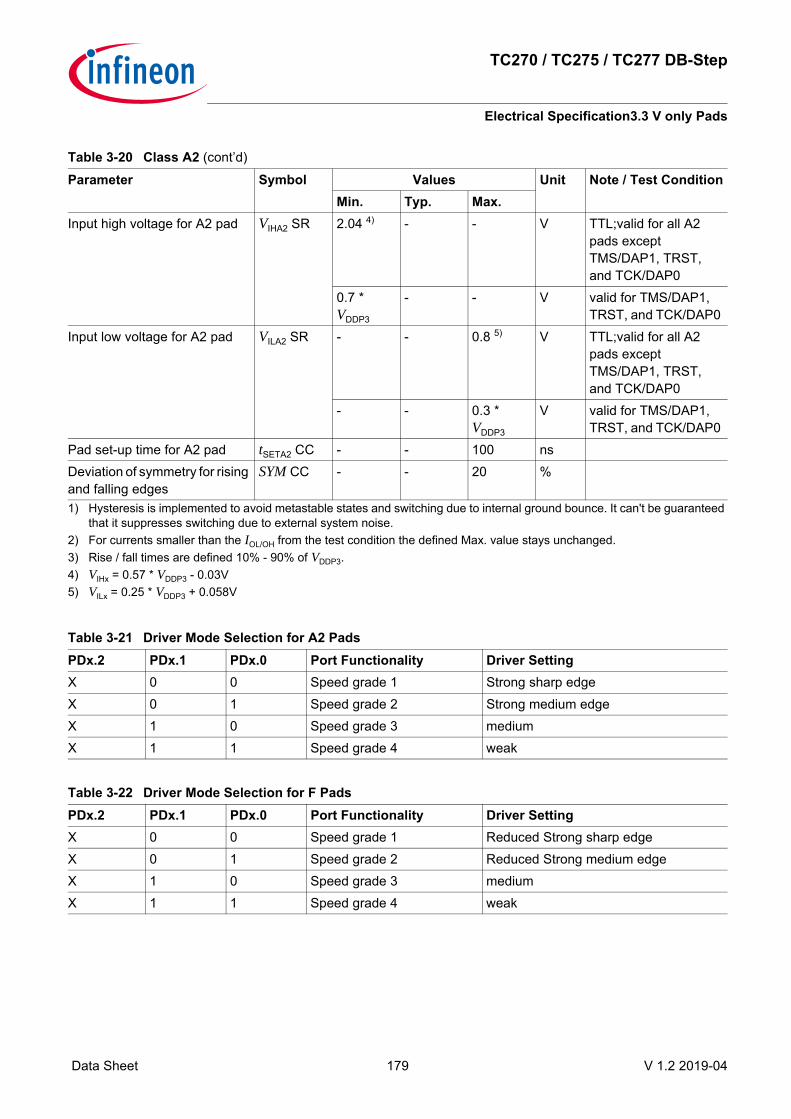
TC270 / TC275 / TC277 DB-Step
Electrical Specification3.3 V only Pads
Data Sheet 179 V 1.2 2019-04
Input high voltage for A2 pad VIHA2 SR 2.04 4) - - V TTL;valid for all A2 pads except TMS/DAP1, TRST, and TCK/DAP0
0.7 * VDDP3
- - V valid for TMS/DAP1, TRST, and TCK/DAP0
Input low voltage for A2 pad VILA2 SR - - 0.8 5) V TTL;valid for all A2 pads except TMS/DAP1, TRST, and TCK/DAP0
- - 0.3 * VDDP3
V valid for TMS/DAP1, TRST, and TCK/DAP0
Pad set-up time for A2 pad tSETA2 CC - - 100 nsDeviation of symmetry for rising and falling edges
SYM CC - - 20 %
1) Hysteresis is implemented to avoid metastable states and switching due to internal ground bounce. It can't be guaranteed that it suppresses switching due to external system noise.
2) For currents smaller than the IOL/OH from the test condition the defined Max. value stays unchanged.3) Rise / fall times are defined 10% - 90% of VDDP3.4) VIHx = 0.57 * VDDP3 - 0.03V5) VILx = 0.25 * VDDP3 + 0.058V
Table 3-21 Driver Mode Selection for A2 PadsPDx.2 PDx.1 PDx.0 Port Functionality Driver SettingX 0 0 Speed grade 1 Strong sharp edgeX 0 1 Speed grade 2 Strong medium edgeX 1 0 Speed grade 3 mediumX 1 1 Speed grade 4 weak
Table 3-22 Driver Mode Selection for F PadsPDx.2 PDx.1 PDx.0 Port Functionality Driver SettingX 0 0 Speed grade 1 Reduced Strong sharp edgeX 0 1 Speed grade 2 Reduced Strong medium edgeX 1 0 Speed grade 3 mediumX 1 1 Speed grade 4 weak
Table 3-20 Class A2 (cont’d)Parameter Symbol Values Unit Note / Test Condition
Min. Typ. Max.

TC270 / TC275 / TC277 DB-Step
Electrical SpecificationHigh performance LVDS Pads (LVDSH)
Data Sheet 180 V 1.2 2019-04
3.7 High performance LVDS Pads (LVDSH)This LVDS pad type is used for the high speed chip to chip communication inferface of the new TC270 / TC275 /TC277. It compose out of a LVDSH pad and a Class F pad.This pad combination is always supplied by the 3.3V supply rail.
Table 3-23 Class FParameter Symbol Values Unit Note / Test Condition
Min. Typ. Max.Input frequency fIN SR - - 75 MHzInput Hysteresis for F pad 1) HYSF CC 0.1 *
VDDP3 - - V TTL
Input Leakage Current for F pad
IOZF CC -1000 - 1000 nA (0.1*VDDP3) < VIN < (0.9*VDDP3); valid for P21.2 and P21.3; TJ = 150°C
-1500 - 1500 nA (0.1*VDDP3) < VIN < (0.9*VDDP3); valid for P21.2 and P21.3; TJ = 170°C
-300 - 300 nA (0.1*VDDP3) < VIN < (0.9*VDDP3); valid for P21.4 and P21.5
-2000 - 2000 nA else; valid for P21.2 and P21.3; TJ = 150°C
-3000 - 3000 nA else; valid for P21.2 and P21.3; TJ = 170°C
-600 - 600 nA else; valid for P21.4 and P21.5
Pull-up current for F pad IPUHF CC |25| - - µA VIHmin
- - |100| µA VILmax
Pull-down current for class F pads
IPDLF CC - - |100| µA VIHmin
|25| - - µA VILmax
On resistance for F pad, weak driver 2)
RDSONFW CC
100 200 325 Ohm PMOS/NMOS ; IOH=0.5mA ; IOL=0.5mA
On resistance for F pad, medium driver 2)
RDSONFM CC
40 70 100 Ohm PMOS/NMOS ; IOH=2mA ; IOL=2mA
On resistance for F pad, strong driver 2)
RDSONFS CC 20 50 80 Ohm PMOS/NMOS ; IOH=4mA ; IOL=4mA

TC270 / TC275 / TC277 DB-Step
Electrical SpecificationHigh performance LVDS Pads (LVDSH)
Data Sheet 181 V 1.2 2019-04
CL = 2.5 pF for all LVDSH parameters.
Rise/fall time for F pad 3) trfF CC - - 20+0.8*CL
ns CL≤50pF ; pin out driver=weak
- - 17.5+0.85*CL
ns CL≥50pF ; CL≤200pF ; pin out driver=weak
- - 12+0.16*CL
ns CL≤50pF ; pin out driver=medium
- - 11.5+0.17*CL
ns CL≥50pF ; CL≤200pF ; pin out driver=medium
- - 7+0.16*CL
ns CL≤50pF ; edge=medium ; pin out driver=reduced strong
- - 6.5+0.17*CL
ns CL≥50pF ; CL≤200pF ; edge=meduim ; pin out driver>reduced strong
- - 4+0.16*CL
ns CL≤50pF ; edge=sharp ; pin out driver=reduced strong
- - 3.5+0.17*CL
ns CL≥50pF ; CL≤200pF ; edge=sharp ; pin out driver=reduced strong
Input high voltage for F pad VIHF SR 2.04 4) - - V TTLInput low voltage for F pad VILF SR - - 0.8 5) V TTLPad set-up time for F pad tSETF CC - - 100 nsDeviation of symmetry for rising and falling edges
SYM CC - - 20 %
1) Hysteresis is implemented to avoid metastable states and switching due to internal ground bounce. It can't be guaranteed that it suppresses switching due to external system noise.
2) For currents smaller than the IOL/OH from the test condition the defined Max. value stays unchanged.3) Rise / fall times are defined 10% - 90% of VDDP3.4) VIHx = 0.57 * VDDP3 - 0.03V5) VILx = 0.25 * VDDP3 + 0.058V
Table 3-24 LVDSH - IEEE standard LVDS general purpose link (GPL)Parameter Symbol Values Unit Note / Test Condition
Min. Typ. Max.Output impedance R0 CC 40 - 140 Ohm Vcm = 1.0 V and 1.4 VRise time 1) trise20 CC - - 0.5 ns ZL = 100 Ohm ±5%
@2 pFFall time 1) tfall20 CC - - 0.5 ns ZL = 100 Ohm ±5% @
2 pFOutput differential voltage VOD CC 250 - 400 mV RT = 100 Ohm ±5%
Table 3-23 Class F (cont’d)Parameter Symbol Values Unit Note / Test Condition
Min. Typ. Max.

TC270 / TC275 / TC277 DB-Step
Electrical SpecificationHigh performance LVDS Pads (LVDSH)
Data Sheet 182 V 1.2 2019-04
Output voltage high VOH CC - - 1475 mV RT = 100 Ohm ±5% (400 mV/2) + 1275 mV
Output voltage low VOL CC 925 - - mV RT = 100 Ohm ±5%Output offset (Common mode) voltage
VOS CC 1125 - 1275 mV RT = 100 Ohm ±5%
Input voltage range VI SR 0 - 1600 mV Driver ground potential difference < 925 mV; RT = 100 Ohm ±10%
0 - 2000 mV Driver ground potential difference < 925 mV; RT = 100 Ohm ±20%
Input differential threshold Vidth SR -100 - 100 mV Driver ground potential difference < 925 mV
Delta output impedance dR0 SR - - 10 % Vcm = 1.0 V and 1.4 V (mismatch Pd and Pn)
Change in VOS between 0 and 1
dVOS CC - - 25 mV RT = 100 Ohm ±5%
Change in Vod between 0 and 1
dVod CC - - 25 mV RT = 100 Ohm ±5%
Duty cycle tduty CC 45 - 55 %1) Rise / fall times are defined for 20% - 80% of VOD
Table 3-25 LVDSH - IEEE standard LVDS reduced link (REDL)Parameter Symbol Values Unit Note / Test Condition
Min. Typ. Max.Output impedance R0 CC 40 - 140 Ohm Vcm = 1.0 V and 1.4 VOutput differential voltage VOD CC 150 - 250 mV RT = 100 Ohm ±5%Output voltage high VOH CC - - 1375 mV RT = 100 Ohm ±5%Output voltage low VOL CC 1025 - - mV RT = 100 Ohm ±5%Output offset (Common mode) voltage
VOS CC 1125 - 1275 mV RT = 100 Ohm ±5%
Input voltage range VI SR 825 - 1575 mV Driver ground potential difference < 50 mV
Input differential threshold Vidth SR -100 - 100 mV Driver ground potential difference < 50 mV
Change in VOS between 0 and 1
dVOS CC - - 25 mV RT = 100 Ohm ±5%
Change in Vod between 0 and 1
dVod CC - - 25 mV RT = 100 Ohm ±5%
Duty cycle tduty CC 45 - 55 %
Table 3-24 LVDSH - IEEE standard LVDS general purpose link (GPL) (cont’d)Parameter Symbol Values Unit Note / Test Condition
Min. Typ. Max.

TC270 / TC275 / TC277 DB-Step
Electrical SpecificationHigh performance LVDS Pads (LVDSH)
Data Sheet 183 V 1.2 2019-04
default after start-up = CMOS function
VOD Fall time 1) tfall10 CC - - 0.5 ns ZL = 100 Ohm ±5% @ 2pF
VOD Rise time 1) trise10 CC - - 0.5 ns ZL = 100 Ohm ±5% @ 2pF
1) Rise / fall times are defined for 10% - 90% of VOD
Table 3-25 LVDSH - IEEE standard LVDS reduced link (REDL) (cont’d)Parameter Symbol Values Unit Note / Test Condition
Min. Typ. Max.

TC270 / TC275 / TC277 DB-Step
Electrical SpecificationMedium performance LVDS Pads (LVDSM)
Data Sheet 184 V 1.2 2019-04
3.8 Medium performance LVDS Pads (LVDSM)This LVDS pad type is used for the medium speed chip to chip communication inferface of the new TC270 / TC275/ TC277. It compose out of a LVDSM pad and a MP pad.This pad combination is always supplied by the 5V or 3.3V.For the parameters of the MP pad please see Chapter 3.5.
default after start-up = CMOS function
Table 3-26 LVDSMParameter Symbol Values Unit Note / Test Condition
Min. Typ. Max.Output impedance RO CC 40 100 140 OhmFall time tF CC - - 2.5 ns Zload = 100 Ohm;
termination 100 Ohm ±1%
Rise time tR CC - - 2.5 ns Zload = 100 Ohm; termination 100 Ohm ±1%
Pad set-up time tSET_LVDS CC
- 10 13 µs
Output Differential Voltage VOD CC 250 - 400 mV termination 100 Ohm ±1%
Output voltage high VOH CC - - 1475 mV termination 100 Ohm ±1%
Output voltage low VOL CC 925 - - mV termination 100 Ohm ±1%
Output Offset Voltage VOS CC 1125 - 1275 mV termination 100 Ohm ±1%

TC270 / TC275 / TC277 DB-Step
Electrical SpecificationVADC Parameters
Data Sheet 185 V 1.2 2019-04
3.9 VADC ParametersVADC parameter are valid for VDDM = 4.5 V to 5.5 V.This tables also covers the parameters for Class D pads.
Table 3-27 VADCParameter Symbol Values Unit Note / Test Condition
Min. Typ. Max.Analog reference voltage 1) VAREF SR VAGND +
1.0 - VDDM +
0.05 V
Analog reference ground VAGND SR VSSM - 0.05
- VSSM + 0.05
V
Analog input voltage range VAIN SR VAGND - VAREF VConverter reference clock fADCI SR 2 - 20 MHzCharge consumption per conversion 2) 3)
QCONV CC - 50 75 pC VAIN = 5 V, charge consumed from reference pin, precharging disabled
- 10 22 pC VAIN = 5 V, charge consumed from reference pin, precharging enabled
Conversion time for 12-bit result
tC12 CC - (16 + STC) x tADCI + 2 x tVADC
- Includes sample time and post calibration
Conversion time for 10-bit result
tC10 CC - (14 + STC) x tADCI + 2 x tVADC
- Includes sample time
Conversion time for 8-bit result tC8 CC - (12 + STC) x tADCI + 2 x tVADC
- Includes sample time
Conversion time for fast compare mode
tCF CC - (4 + STC) x tADCI + 2 x tVADC
- Includes sample time
Broken wire detection delay against VAGND 4)
tBWG CC - - 120 cycles Result below 10%
Broken wire detection delay against VAREF 5)
tBWR CC - - 60 cycles Result above 80%
Input leakage at analog inputs IOZ1 CC -350 - 350 nA Analog Inputs overlaid with class LP pads or pull down diagnostics
-150 - 150 nA elseTotal Unadjusted Error 1) TUE CC -4 6) - 4 6) LSB 12-bit resolution

TC270 / TC275 / TC277 DB-Step
Electrical SpecificationVADC Parameters
Data Sheet 186 V 1.2 2019-04
INL Error EAINL CC -3 - 3 LSB 12-bit resolutionGain Error 1) EAGAIN CC -3.5 - 3.5 LSB 12-bit resolutionDNL error 1) EADNL CC -3 - 3 LSB 12-bit resolutionOffset Error 1) EAOFF CC -4 - 4 LSB 12-bit resolutionTotal capacitance of an analog input
CAINT CC - - 30 pF
Switched capacitance of an analog input
CAINS CC 2 4 7 pF
Resistance of the analog input path
RAIN CC - - 1.5 kOhm else- - 1.8 kOhm valid for analog inputs
mapped to GPIOsSwitched capacitance of a reference input
CAREFS CC - - 30 pF
RMS Noise 7) ENRMS CC - 0.5 0.8 6)8) LSBPositive reference VAREFx pin leakage
IOZ2 CC -7 - 7 µA VAREFx = VAREF2; VAREF>VDDMV; TJ>150°C
-4 - 4 µA VAREFx = VAREF2; VAREF>VDDMV; TJ≤150°C
-2 - 3 µA VAREFx = VAREF2; VAREF≤VDDMV; TJ>150°C
-1 - 1 µA VAREFx = VAREF2; VAREF≤VDDMV; TJ≤150°C
Negative reference VAGNDx pin leakage
IOZ3 CC -13 - 13 µA VAGNDx = VAGND2; VAGND<VSSMV; TJ>150°C
-7 - 7 µA VAGNDx = VAGND2; VAGND<VSSMV; TJ≤150°C
-3.3 - 2.5 µA VAGNDx = VAGND2; VAREF≤VDDMV; TJ>150°C
-2.85 - 1 µA VAGNDx = VAGND2; VAREF≤VDDMV; TJ≤150°C
Resistance of the reference input path
RAREF CC - - 1 kOhm
CSD resistance 9) RCSD CC - - 28 kOhm
Table 3-27 VADC (cont’d)Parameter Symbol Values Unit Note / Test Condition
Min. Typ. Max.

TC270 / TC275 / TC277 DB-Step
Electrical SpecificationVADC Parameters
Data Sheet 187 V 1.2 2019-04
The following VADC parameter are valid for VDDM = 2.97 V to 3.63 V.
Resistance of the multiplexer diagnostics pull-down device
RMDD CC 25 + 1*VIN - 35 - 8*VIN kOhm 0 V ≤ VIN ≤ 2.5 V-5 + 13*VIN
- 15 + 16*VIN
kOhm 2.5 V ≤ VIN ≤ VDDM
Resistance of the multiplexer diagnostics pull-up device
RMDU CC 45 - 6*VIN - 90 - 16*VIN
kOhm 0 V ≥ VIN ≤ 2.5 V
40 - 4*VIN - 65 - 6*VIN kOhm 2.5 V ≤ VIN ≤ VDDM
Resistance of the pull-down test device 10)
RPDD CC - - 0.3 kOhm
CSD voltage accuracy 11) 12) dVCSD CC - - 10 %Wakeup time tWU CC - - 12 µs1) If the reference voltage is reduced by the factor k (k < 1), TUE,DNL,INL,Gain, and Offset errors increase also by the factor
1/k. VAREF must be decoupled with an external capacitor.2) For QCONV = X pC and a conversion time of 1 µs a rms value of X µA results for IAREFx.3) For the details of the mapping for a VADC group to pin VAREFx please see the User's Manual.4) The broken wire detection delay against VAGND is measured in numbers of consecutive precharge cycles at a conversion
rate higher than 1 conversion per 500 ms.5) The broken wire detection delay against VAREF is measured in numbers of consecutive precharge cycles at a conversion
rate higher than 1 conversion per 10 ms. This function is influenced by leakage current, in particular at high temperature.6) Resulting worst case combined error is arithmetic combination of TUE and ENRMS.7) This parameter is valid for soldered devices and requires careful analog board design.8) Value is defined for one sigma Gauss distribution.9) In order to avoid an additional error due to incomplete sampling, the sampling time shall be set greater than 5 * RCSD * CAINS.10) The pull-down resistor RPDD is connected between the input pad and the analog multiplexer. The input pad
itself adds another 200-Ohm series resistance, when measuring through the pin.11) CSD: Converter Self Diagnostics, for details please consult the User's Manual.12) Note, that in case CSD voltage is chosen to nom. 1/3 or 2/3 of VAREF voltage, the reference voltage is loaded with a current
of max. VAREF / 45 kOhm.
Table 3-28 VADC_33VParameter Symbol Values Unit Note / Test Condition
Min. Typ. Max.Analog reference voltage 1) VAREF SR VAGND +
1.0 - VDDM +
0.05 V
Analog reference ground VAGND SR VSSM - 0.05
- VSSM + 0.05
V
Analog input voltage range VAIN SR VAGND - VAREF VConverter reference clock fADCI SR 2 - 20 MHz
Table 3-27 VADC (cont’d)Parameter Symbol Values Unit Note / Test Condition
Min. Typ. Max.

TC270 / TC275 / TC277 DB-Step
Electrical SpecificationVADC Parameters
Data Sheet 188 V 1.2 2019-04
Charge consumption per conversion 2) 3)
QCONV CC - 35 50 pC VAIN = 3.3 V, charge consumed from reference pin, precharging disabled
- 8 17 pC VAIN = 3.3 V, charge consumed from reference pin, precharging enabled
Conversion time for 12-bit result
tC12 CC - (16 + STC) x tADCI + 2 x tVADC
- Includes sample time and post calibration
Conversion time for 10-bit result
tC10 CC - (14 + STC) x tADCI + 2 x tVADC
- Includes sample time
Conversion time for 8-bit result tC8 CC - (12 + STC) x tADCI + 2 x tVADC
- Includes sample time
Conversion time for fast compare mode
tCF CC - (4 + STC) x tADCI + 2 x tVADC
- Includes sample time
Broken wire detection delay against VAGND 4)
tBWG CC - - 120 cycles Result below 10%
Broken wire detection delay against VAREF 5)
tBWR CC - - 60 cycles Result above 80%
Input leakage at analog inputs IOZ1 CC -350 - 350 nA Analog Inputs overlaid with class LP pads or pull down diagnostics
-150 - 150 nA elseTotal Unadjusted Error 1) TUE CC -12 6) - 12 6) LSB 12-bit Resolution; TJ >
150 °C-6 6) - 6 6) LSB 12-bit Resolution; TJ ≤
150 °CINL Error EAINL CC -12 - 12 LSB 12-bit Resolution; TJ >
150 °C-5 - 5 LSB 12-bit Resolution; TJ ≤
150 °CGain Error 1) EAGAIN CC -6 - 6 LSB 12-bit Resolution; TJ >
150 °C-5.5 - 5.5 LSB 12-bit Resolution; TJ ≤
150 °C
Table 3-28 VADC_33V (cont’d)Parameter Symbol Values Unit Note / Test Condition
Min. Typ. Max.
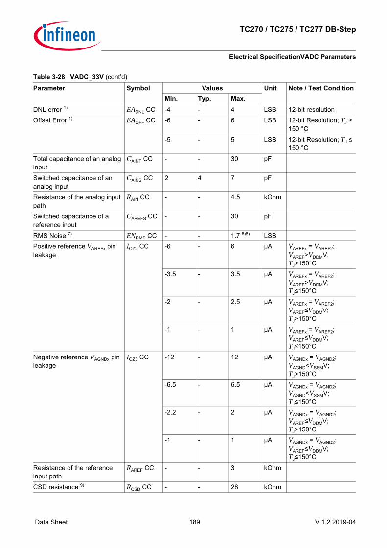
TC270 / TC275 / TC277 DB-Step
Electrical SpecificationVADC Parameters
Data Sheet 189 V 1.2 2019-04
DNL error 1) EADNL CC -4 - 4 LSB 12-bit resolutionOffset Error 1) EAOFF CC -6 - 6 LSB 12-bit Resolution; TJ >
150 °C-5 - 5 LSB 12-bit Resolution; TJ ≤
150 °CTotal capacitance of an analog input
CAINT CC - - 30 pF
Switched capacitance of an analog input
CAINS CC 2 4 7 pF
Resistance of the analog input path
RAIN CC - - 4.5 kOhm
Switched capacitance of a reference input
CAREFS CC - - 30 pF
RMS Noise 7) ENRMS CC - - 1.7 6)8) LSBPositive reference VAREFx pin leakage
IOZ2 CC -6 - 6 µA VAREFx = VAREF2; VAREF>VDDMV; TJ>150°C
-3.5 - 3.5 µA VAREFx = VAREF2; VAREF>VDDMV; TJ≤150°C
-2 - 2.5 µA VAREFx = VAREF2; VAREF≤VDDMV; TJ>150°C
-1 - 1 µA VAREFx = VAREF2; VAREF≤VDDMV; TJ≤150°C
Negative reference VAGNDx pin leakage
IOZ3 CC -12 - 12 µA VAGNDx = VAGND2; VAGND<VSSMV; TJ>150°C
-6.5 - 6.5 µA VAGNDx = VAGND2; VAGND<VSSMV; TJ≤150°C
-2.2 - 2 µA VAGNDx = VAGND2; VAREF≤VDDMV; TJ>150°C
-1 - 1 µA VAGNDx = VAGND2; VAREF≤VDDMV; TJ≤150°C
Resistance of the reference input path
RAREF CC - - 3 kOhm
CSD resistance 9) RCSD CC - - 28 kOhm
Table 3-28 VADC_33V (cont’d)Parameter Symbol Values Unit Note / Test Condition
Min. Typ. Max.

TC270 / TC275 / TC277 DB-Step
Electrical SpecificationVADC Parameters
Data Sheet 190 V 1.2 2019-04
Figure 3-1 Equivalent Circuitry for Analog Inputs
Resistance of the multiplexer diagnostics pull-down device
RMDD CC 25 + 3*VIN - 40 + 12*VIN
kOhm 0 V ≤ VIN ≤ 1.667 V
0 + 18*VIN - 0 + 18*VIN kOhm 1.667 V ≤ VIN ≤ VDDM
Resistance of the multiplexer diagnostics pull-up device
RMDU CC 60 - 12*VIN
- 120 - 30*VIN
kOhm 0 V ≤ VIN ≤ 1.667 V
55 - 9*VIN - 95 - 15*VIN
kOhm 1.667 V ≤ VIN ≤ VDDM
Resistance of the pull-down test device 10)
RPDD CC - - 0.9 kOhm
CSD voltage accuracy 11) 12) dVCSD CC - - 10 %Wakeup time tWU CC - - 12 µs1) If the reference voltage is reduced by the factor k (k < 1), TUE,DNL,INL,Gain, and Offset errors increase also by the factor
1/k. VAREF must be decoupled with an external capacitor.2) For QCONV = X pC and a conversion time of 1 µs a rms value of X µA results for IAREFx.3) For the details of the mapping for a VADC group to pin VAREFx please see the User's Manual.4) The broken wire detection delay against VAGND is measured in numbers of consecutive precharge cycles at a conversion
rate higher than 1 conversion per 500 ms.5) The broken wire detection delay against VAREF is measured in numbers of consecutive precharge cycles at a conversion
rate higher than 1 conversion per 10 ms. This function is influenced by leakage current, in particular at high temperature.6) Resulting worst case combined error is arithmetic combination of TUE and ENRMS.7) This parameter is valid for soldered devices and requires careful analog board design.8) Value is defined for one sigma Gauss distribution.9) In order to avoid an additional error due to incomplete sampling, the sampling time shall be set greater than 5 * RCSD * CAINS.10) The pull-down resistor RPDD is connected between the input pad and the analog multiplexer. The input pad
itself adds another 200-Ohm series resistance, when measuring through the pin.11) CSD: Converter Self Diagnostics, for details please consult the User's Manual.12) Note, that in case CSD voltage is chosen to nom. 1/3 or 2/3 of VAREF voltage, the reference voltage is loaded with a current
of max. VAREF / 45 kOhm.
Table 3-28 VADC_33V (cont’d)Parameter Symbol Values Unit Note / Test Condition
Min. Typ. Max.
A/D Converter
MCS05570
RSource
VAIN CExt CAINT CAINS-
RAIN, On
CAINS

TC270 / TC275 / TC277 DB-Step
Electrical SpecificationDSADC Parameters
Data Sheet 191 V 1.2 2019-04
3.10 DSADC ParametersThe following DSADC parameter are valid for VDDM = 4.5 V to 5.5 V.
Table 3-29 DSADCParameter Symbol Values Unit Note / Test Condition
Min. Typ. Max.Analog input voltage range 1) VDSIN SR 0 - 5 V single ended
0 - 10 V differential;VDSxP - VDSxN
Reference load current IREF SR - 4.5 6.3 µA per twin-modulator (1 or 2 channels)
Modulator clock frequency 2) fMOD SR 10 - 20 MHzGain error EDGAIN CC -1 - 1 3) % Calibrated once
-3.5 4) - 3.5 4) % Uncalibrated-0.2 - 0.2 5) % calibrated; GAIN = 1;
MODCFG.INCFGx=01DC offset error EDOFF CC -5 - 5 5) mV calibrated
-50 - 50 mV calibrated once-100 4) 04) 100 4) mV gain = 1; uncalibrated
Common Mode Rejection Ratio EDCM CC 200 500 - Input impedance 6) RDAIN CC 100 130 170 kOhm Exact value (±1%)
available in UCBSignal-Noise Ratio 7) 8) 9) 10) SNR CC 80 - - dB fPB = 30 kHz; VDDM =
±5%; fMOD = 20 MHz; GAIN = 1
78 - - dB fPB = 50 kHz; VDDM = ±5%; fMOD = 20 MHz; GAIN = 1
70 - - dB fPB = 100 kHz; VDDM = ±10%; fMOD = 20 MHz; GAIN = 1
74 - - dB fPB = 100 kHz; VDDM = ±5%; fMOD = 20 MHz; GAIN = 1
76 - - dB fPB = 30 kHz; VDDM = ±10%; fMOD = 20 MHz; GAIN = 1
74 - - dB fPB = 50 kHz; VDDM = ±10%; fMOD = 20 MHz; GAIN = 1
Pass band fPB CC 10 11) - 100 kHz Output data rate fD = fPB * 3
Pass band ripple 8) dfPB CC -1 - 1 %Output sampling rate fD CC 30 - 330 kHz

TC270 / TC275 / TC277 DB-Step
Electrical SpecificationDSADC Parameters
Data Sheet 192 V 1.2 2019-04
DC compensation factor DCF CC -3 - - dB 10-5 fD
Positive reference VAREF1 pin leakage
IOZ5 CC -2 - 2 µA all ADCs disabled
Negative reference VAGND1 pin leakage
IOZ6 CC -2 - 2 µA all ADCs disabled
Stop band attenuation 8) SBA CC 40 - - dB 0.5 ... 1 fD
45 - - dB 1 ... 1.5 fD
50 - - dB 1.5 ... 2 fD
55 - - dB 2 ... 2.5 fD
60 - - dB 2.5 ... OSR/2 fD
Reference ground voltage VAGND SR VSSM - 0.05
- VSSM + 0.05
V
Positive reference voltage VAREF SR VDDMnom * 0.9
- VDDM + 0.05
V
Common mode voltage accuracy
dVCM CC -100 - 100 mV from selected voltage
Common mode hold voltage deviation 12)
dVCMH CC -200 - 200 mV From common mode voltage
Analog filter settling time tAFSET CC - 2 4 µs If enabledModulator recovery time tMREC CC - 3.5 5.5 µs After leaving overdrive
stateModulator settling time 13) tMSET CC - 1 - µs After switching on,
voltage regulator already running
Spurious Free Dynamic Range 7)14)
SFDR CC 60 - - dB VCM = 2.2 V, DC coupled; VDDM = ±10%
1) The maximum input range for symmetrical signals (e.g. AC-coupled inputs) depends on the selected internal/external common mode voltage. In this case the Amplitude is limited to VCM * 2.
2) All modulators must run on the same frequency.3) The calibration sequence must be executed once after an Application Reset4) The total DC error for the uncalibrated case can be calculated by the geometric addition of EDGAIN and EDOFF
5) Recalibration needed in case of a temperature change > 20ºC6) The variation of the impedance between different channels is < 1.5%.7) Derating factors:
-2 dB in standard-performance mode.-3 dB for CMV = 10B, i.e. VCM = (VAREF±2%) / 2.0.
8) CIC3, FIR0, FIR1 filters enabled.9) Single-ended mode reduces the SNR by 6 dB if the unused input is grounded, by 3 dB if the unused input connects to VCM
(GAIN = 2).10) The defined limits are only valid if the following condition is not applicable: TJ > 150°C and VVAREF > VDDM.11) 10 kHz only reachable with 10 MHz modulator clock frequency.12) Voltage VCM is proportional to VAREF, voltage VCMH is proportional to VDDM.13) The modulator needs to settle after being switched on and after leaving the overdrive state.14) SFDR = 20 * log(INL / 2N); N = amount of bits
Table 3-29 DSADC (cont’d)Parameter Symbol Values Unit Note / Test Condition
Min. Typ. Max.
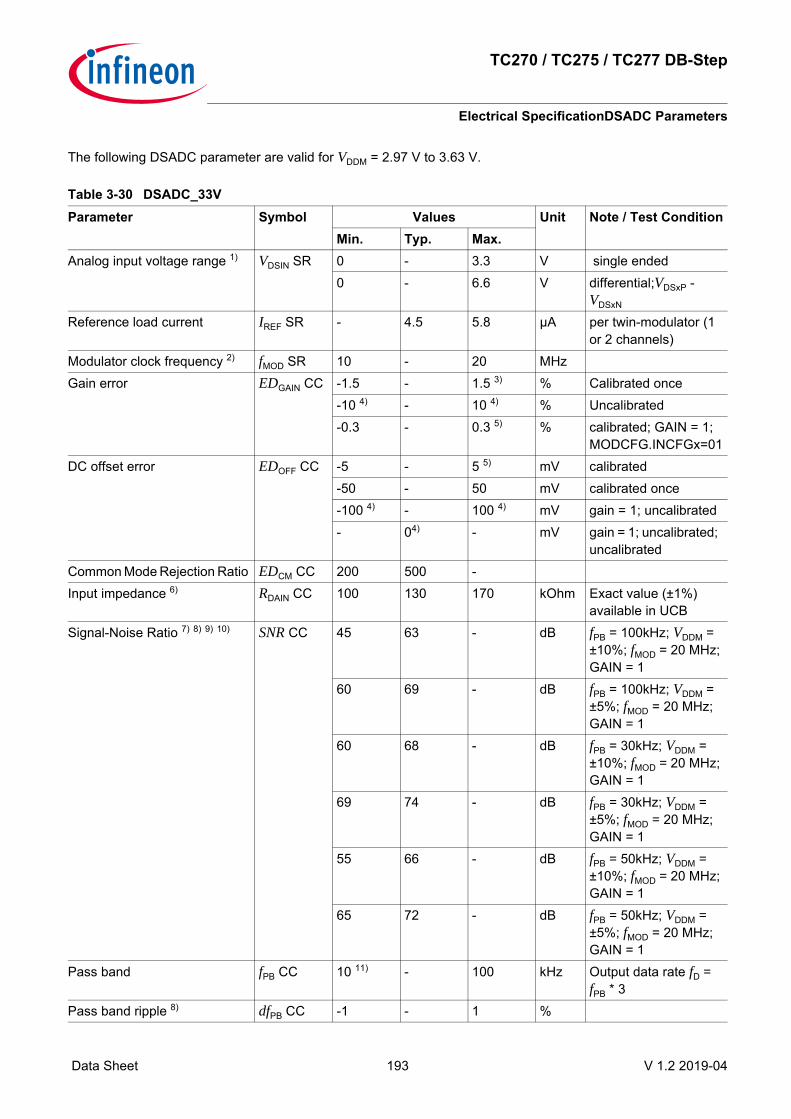
TC270 / TC275 / TC277 DB-Step
Electrical SpecificationDSADC Parameters
Data Sheet 193 V 1.2 2019-04
The following DSADC parameter are valid for VDDM = 2.97 V to 3.63 V.
Table 3-30 DSADC_33VParameter Symbol Values Unit Note / Test Condition
Min. Typ. Max.Analog input voltage range 1) VDSIN SR 0 - 3.3 V single ended
0 - 6.6 V differential;VDSxP - VDSxN
Reference load current IREF SR - 4.5 5.8 µA per twin-modulator (1 or 2 channels)
Modulator clock frequency 2) fMOD SR 10 - 20 MHzGain error EDGAIN CC -1.5 - 1.5 3) % Calibrated once
-10 4) - 10 4) % Uncalibrated-0.3 - 0.3 5) % calibrated; GAIN = 1;
MODCFG.INCFGx=01DC offset error EDOFF CC -5 - 5 5) mV calibrated
-50 - 50 mV calibrated once-100 4) - 100 4) mV gain = 1; uncalibrated- 04) - mV gain = 1; uncalibrated;
uncalibratedCommon Mode Rejection Ratio EDCM CC 200 500 - Input impedance 6) RDAIN CC 100 130 170 kOhm Exact value (±1%)
available in UCBSignal-Noise Ratio 7) 8) 9) 10) SNR CC 45 63 - dB fPB = 100kHz; VDDM =
±10%; fMOD = 20 MHz; GAIN = 1
60 69 - dB fPB = 100kHz; VDDM = ±5%; fMOD = 20 MHz; GAIN = 1
60 68 - dB fPB = 30kHz; VDDM = ±10%; fMOD = 20 MHz; GAIN = 1
69 74 - dB fPB = 30kHz; VDDM = ±5%; fMOD = 20 MHz; GAIN = 1
55 66 - dB fPB = 50kHz; VDDM = ±10%; fMOD = 20 MHz; GAIN = 1
65 72 - dB fPB = 50kHz; VDDM = ±5%; fMOD = 20 MHz; GAIN = 1
Pass band fPB CC 10 11) - 100 kHz Output data rate fD = fPB * 3
Pass band ripple 8) dfPB CC -1 - 1 %

TC270 / TC275 / TC277 DB-Step
Electrical SpecificationDSADC Parameters
Data Sheet 194 V 1.2 2019-04
Output sampling rate fD CC 30 - 330 kHzDC compensation factor DCF CC -3 - - dB 10-5 fD
Positive reference VAREF1 pin leakage
IOZ5 CC -2 - 2 µA
Negative reference VAGND1 pin leakage
IOZ6 CC -2 - 2 µA
Stop band attenuation 8) SBA CC 40 - - dB 0.5 ... 1 fD
45 - - dB 1 ... 1.5 fD
50 - - dB 1.5 ... 2 fD
55 - - dB 2 ... 2.5 fD
60 - - dB 2.5 ... OSR/2 fD
Reference ground voltage VAGND SR VSSM - 0.05
- VSSM + 0.05
V
Positive reference voltage VAREF SR VDDMnom * 0.9
- VDDM + 0.05
V
Common mode voltage accuracy
dVCM CC -100 - 100 mV from selected voltage
Common mode hold voltage deviation 12)
dVCMH CC -200 - 200 mV From common mode voltage
Analog filter settling time tAFSET CC - 2 4 µs If enabledModulator recovery time tMREC CC - 3.5 - µs After leaving overdrive
stateModulator settling time 13) tMSET CC - 1 - µs After switching on,
voltage regulator already running
Spurious Free Dynamic Range 7)14)
SFDR CC 52 - - dB VCM = 2.2 V, DC coupled; VDDM = ±10%
60 - - dB VCM = 2.2 V, DC coupled; VDDM = ±5%
1) The maximum input range for symmetrical signals (e.g. AC-coupled inputs) depends on the selected internal/external common mode voltage. In this case the Amplitude is limited to VCM * 2.
2) All modulators must run on the same frequency.3) The calibration sequence must be executed once after an Application Reset4) The total DC error for the uncalibrated case can be calculated by the geometric addition of EDGAIN and EDOFF
5) Recalibration needed in case of a temperature change > 20ºC.6) The variation of the impedance between different channels is < 1.5%.7) Derating factors:
-2 dB in standard-performance mode.-3 dB for CMV = 10B, i.e. VCM = (VAREF±2%) / 2.0.
8) CIC3, FIR0, FIR1 filters enabled.9) Single-ended mode reduces the SNR by 6 dB if the unused input is grounded, by 3 dB if the unused input connects to VCM
(GAIN = 2).10) The defined limits are only valid if the following condition is not applicable: TJ > 150°C and VVAREF > VDDM.
Table 3-30 DSADC_33V (cont’d)Parameter Symbol Values Unit Note / Test Condition
Min. Typ. Max.

TC270 / TC275 / TC277 DB-Step
Electrical SpecificationDSADC Parameters
Data Sheet 195 V 1.2 2019-04
Figure 3-2 DSADC Analog Inputs
11) 10 kHz bandwidth only with 10Mhz modulator clock frequency reachable12) Voltage VCM is proportional to VAREF, voltage VCMH is proportional to VDDM.13) The modulator needs to settle after being switched on and after leaving the overdrive state.14) SFDR = 20 * log(INL / 2N); N = amount of bits
MC_DSADC_MODULATORBLOCK
Inpu
t Modu-lator
130 kΩ
VCM
Gain
Gain
37 k
Ω
130 kΩ
37 k
Ω
=VOFFSET

TC270 / TC275 / TC277 DB-Step
Electrical SpecificationMHz Oscillator
Data Sheet 196 V 1.2 2019-04
3.11 MHz OscillatorOSC_XTAL is used as accurate and exact clock source. OSC_XTAL supports 8 MHz to 40 MHz crystals externaloutside of the device. Support of ceramic resonators is also provided.
Note: It is strongly recommended to measure the oscillation allowance (negative resistance) in the final target system (layout) to determine the optimal parameters for the oscillator operation. Please refer to the limits specified by the crystal or ceramic resonator supplier.
Table 3-31 OSC_XTALParameter Symbol Values Unit Note / Test Condition
Min. Typ. Max.Input current at XTAL1 IIX1 CC -25 - 25 µA VIN>0V ; VIN<VDDP3VOscillator frequency fOSC SR 4 - 40 MHz Direct Input Mode
selected8 - 40 MHz External Crystal Mode
selectedOscillator start-up time 1)
1) tOSCS is defined from the moment when VDDP3 = 3.13V until the oscillations reach an amplitude at XTAL1 of 0.3 * VDDP3. The external oscillator circuitry must be optimized by the customer and checked for negative resistance as recommended and specified by crystal suppliers.
tOSCS CC - - 5 2)
2) This value depends on the frequency of the used external crystal. For faster crystal frequencies this value decrease.
msInput high voltage at XTAL1 VIHBX SR 0.8 - VDDP3 +
0.5 V If shaper is bypassed
Input low voltage at XTAL1 VILBX SR -0.5 - 0.4 V If shaper is bypassedInput voltage at XTAL1 VIX SR -0.5 - VDDP3 +
0.5 V If shaper is not
bypassedInput amplitude (peak to peak) at XTAL1
VPPX SR 0.3 * VDDP3
- VDDP3 + 1.0
V If shaper is not bypassed; fOSC > 25MHz
0.4 * VDDP3
- VDDP3 + 1.0
V If shaper is not bypassed; fOSC ≤ 25MHz
Internal load capacitor CL0 CC 2 2.35 2.7 pFInternal load capacitor CL1 CC 2 2.35 2.7 pFInternal load capacitor CL2 CC 3 3.5 4 pFInternal load capacitor CL3 CC 5.1 5.9 6.6 pF

TC270 / TC275 / TC277 DB-Step
Electrical SpecificationBack-up Clock
Data Sheet 197 V 1.2 2019-04
3.12 Back-up ClockThe back-up clock provides an alternative clock source.
Table 3-32 Back-up ClockParameter Symbol Values Unit Note / Test Condition
Min. Typ. Max.Back-up clock before trimming fBACKUT CC 75 100 125 MHz VEXT≥2.97VBack-up clock after trimming fBACKT CC 97.5 100 102.5 MHz VEXT≥2.97V

TC270 / TC275 / TC277 DB-Step
Electrical SpecificationTemperature Sensor
Data Sheet 198 V 1.2 2019-04
3.13 Temperature Sensor
The following formula calculates the temperature measured by the DTS in [oC] from the RESULT bit field of theDTSSTAT register.
(3.1)
Table 3-33 DTSParameter Symbol Values Unit Note / Test Condition
Min. Typ. Max.Measurement time tM CC - - 100 µsCalibration reference accuracy TCALACC CC -1 - 1 °C calibration points @
TJ=-40°C and TJ=127°C
Non-linearity accuracy over temperature range
TNL CC -2 - 2 °C
Temperature sensor range TSR SR -40 - 170 °CStart-up time after resets inactive
tTSST SR - - 20 µs
Tj DTSSTATRESULT 607( )–2 13,
----------------------------------------------------------------------------=

TC270 / TC275 / TC277 DB-Step
Electrical SpecificationPower Supply Current
Data Sheet 199 V 1.2 2019-04
3.14 Power Supply CurrentThe total power supply current defined below consists of leakage and switching component.Application relevant values are typically lower than those given in the following table and depend on the customer'ssystem operating conditions (e.g. thermal connection or used application configurations).The operating conditions for the parameters in the following table are:The real (realisic) power pattern defines the following conditions:• TJ = 150 °C• fSRI = fMAX = fCPU0 = 200 MHz• fSPB = fSTM = fGTM = fBAUD1 = fBAUD2 = fASCLIN = 40 MHz• VDD = 1.326 V• VDDP3 = 3.366 V• VEXT / FLEX = VDDM = 5.1 V• all cores are active including one lockstep core• the following peripherals are inactive: HSM, HSCT, Ethernet, PSI5, I2C, FCE, MTU, and 50% of the DSADC
channelsThe max power pattern defines the following conditions:• TJ = 150 °C• fSRI = fMAX = fCPU0 = 200 MHz• fSPB = fSTM = fGTM = fBAUD1 = fBAUD2 = fASCLIN = 100 MHz• VDD = 1.43 V• VDDP3 = 3.63 V• VEXT / FLEX = VDDM = 5.5 V• all cores and lockstep cores are active• all peripherals are active
Table 3-34 Power SupplyParameter Symbol Values Unit Note / Test Condition
Min. Typ. Max.∑ Sum of IDD 1.3 V core and peripheral supply currents
IDD CC - - 550 mA max power pattern- - 350 mA real power pattern
IDD core current during active power-on reset (PORST held low)
IDDPORST CC
- - 80 mA TJ=125°C- - 160 mA TJ=150°C- - 215 mA TJ=165°C
IDD core current of CPU0 lockstep core active
IDDC01 CC - - 36 mA real power pattern
IDD core current of CPU1 main core with CPU1 lockstep core inactive
IDDC10 CC - - 43 mA real power pattern
IDD core current of CPU1 main core with lockstep core active
IDDC11 CC - - IDDC10 + 36
mA real power pattern
IDD core current of CPU2 main core
IDDC20 CC - - 37 mA real power pattern

TC270 / TC275 / TC277 DB-Step
Electrical SpecificationPower Supply Current
Data Sheet 200 V 1.2 2019-04
IDD core current added by HSM IDDHSM CC - - 20 mA HSM running at 100MHz.
∑ Sum of 3.3 V supply currents without pad activity
IDDx3RAIL CC - - 57 mA real power pattern
IDDFL3 Flash memory current IDDFL3 CC - - 42 1) mA flash read current- - 42 2) mA flash read current
while programming Dflash
IDDP3 supply current without pad activity
IDDP3 CC - - 15 1) mA real power pattern; incl. OSC current & flash read current
- - 37 3) mA incl. OSC current and flash 3.3V programming current when using external 5V supply
- - 39 2) mA incl. OSC current and flash programming current at 3.3V
IDDP3 supply current for LVDSH pads in LVDS mode
IDDP3LVDSH CC
- - 16 mA
Σ Sum of external and ADC supply currents (incl. IEXTFLEX+IDDM+IEXTLVDSM)
IEXTRAIL CC - - 62 mA real power pattern
Sum of IEXT and IFLEX supply current without pad activity
IEXT/FLEX CC - - 4 mA real power pattern; PORST output inactive.
IEXT supply current for LVDSM pads in LVDS mode
IEXTLVDSM CC
- - 14 4) mA real power pattern
Table 3-34 Power Supply (cont’d)Parameter Symbol Values Unit Note / Test Condition
Min. Typ. Max.

TC270 / TC275 / TC277 DB-Step
Electrical SpecificationPower Supply Current
Data Sheet 201 V 1.2 2019-04
IDDM supply current IDDM CC - - 44 mA real power pattern; sum of currents of DSADC and VADC modules
- - 30 mA current for DSADC module only; 50% DSADC channels active.
- - 14 mA real pattern; current for VADC only
- - 59 5) mA max power pattern; All DSADC channels active 100% time.
- - 17 6) mA max power pattern; All VADC converters are active 100% time
Σ Sum of all currents (incl. IEXTRAIL+IDDx3RAIL+IDD)
IDDTOT CC - - 469 mA real power pattern
Σ Sum of all currents with DC-DC EVR13 regulator active 7)
IDDTOTDC3 CC
- - 302 mA real power pattern; VEXT = 3.3V
Σ Sum of all currents with DC-DC EVR13 regulator active 7)
IDDTOTDC5 CC
- - 240 mA real power pattern; VEXT = 5V
∑ Sum of all currents (STANDBY mode)
IEVRSB CC - - 150 8) µA Standby RAM is active. Power to remaining domains switched off. TJ = 25°C; VEVRSB = 5V
∑ Sum of all currents (SLEEP mode)
ISLEEP CC - - 15 mA All CPUs in idle, All peripherals in sleep, fSRI/SPB = 1 MHz via LPDIV divider; TJ = 25°C
Maximum power dissipation PD CC - - 1480 mW max power pattern- - 1014 mW real power pattern
1) Realistic Pflash read pattern with 70% Pflash bandwidth utlilization and a code mix of 50% 0s and 50% 1s. A common decoupling capacitor of atleast 100nF for (VDDFL3+VDDP3) is used. Dflash read current is also included. Flash read current is predominantly drawn from VDDFL3 pin and a minor part drawn from the neighbouring VDDP3 pin.
2) Continuous Dflash programming in burst mode with 3.3 V supply and realistic Pflash read access in parallel. Erase currents of the corresponding flash modules are less than the respective programming currents at VDDP3 pin. Programming and erasing flash may generate transient current spikes of up to x mA for maximum x us which is handled by the decoupling and buffer capacitors. This parameter is relevant for external power supply dimensioning and not for thermal considerations.
3) In addition to the current specified, upto 4 mA is additionally drawn at VEXT supply in burst programming mode with 5V external supply. Erase currents of the corresponding flash modules are less than the respective programming currents at VDDP3 supply. This parameter is relevant for external power supply dimensioning and not for thermal considerations.
Table 3-34 Power Supply (cont’d)Parameter Symbol Values Unit Note / Test Condition
Min. Typ. Max.

TC270 / TC275 / TC277 DB-Step
Electrical SpecificationPower Supply Current
Data Sheet 202 V 1.2 2019-04
3.14.1 Calculating the 1.3 V Current ConsumptionThe current consumption of the 1.3 V rail compose out of two parts:• Static current consumption• Dynamic current consumptionThe static current consumption is related to the device temperature TJ and the dynamic current consumptiondepends of the configured clocking frequencies and the software application executed. These two parts needs tobe added in order to get the rail current consumption.
(3.2)
(3.3)
Function 2 defines the typical static current consumption and Function 3 defines the maximum static currentconsumption. Both functions are valid for VDD = 1.326 V.
4) The current consumption is for 2 pairs of LVDSM differential pads (8 pins). A single pair of LVDSM differential pads (4 pins) consumes 7 mA.
5) The current consumption is for 6 DS channels with standard performance (MCFG=11b). A single DS channel instance consumes 6-8 mA.
6) A single converter instance of VADC unit consumes 2 mA.7) The total current drawn from external regulator is estimated with 72% EVR13 SMPS regulator Efficiency. IDDTOTDCx is
calculated from IDDTOT using the scaled core current [(IDD x VDD)/(VinxEfficiency)] and constitutes all other rail currents and IDDM.
8) Current at VEVRSB supply pin during normal RUN mode is less than 5 mA at Tj =150 degC. The transition between RUN mode to STANDBY mode has a duration of less than 100us during which the current is higher but is less than 8 mA at Tj =150 degC. Once STANDBY mode is entered with only Standby RAM active the current is less than 5mA at Tj = 150 degC. It is recommended to have atleast 100 nF decoupling capacitor at this pin.
I0 1 135 mAC---------, e0 02689, TJ×× C[ ]=
I0 3 264 mAC---------, e0 0259, TJ×× C[ ]=
TC270 / TC275 / TC277 DB-Step
Electrical SpecificationPower-up and Power-down
Data Sheet 203 V 1.2 2019-04
3.15 Power-up and Power-down
3.15.1 External Supply Mode5 V & 1.3 V supplies are externally supplied. 3.3V is generated internally by EVR33.• External supplies VEXT and VDD may ramp-up or ramp-down independent of each other with regards to start,
rise and fall time(s). Voltage Ramp-up from a residual threshold (Eg : up to 1 V) should also lead to a normal startup of the device.
• The rate at which current is drawn from the external regulator (dIEXT /dt or dIDD /dt) is limited in the Start-up phase to a maximum of 50 mA/100 us.
• PORST is active/asserted when either PORST (input) or PORST (output) is active/asserted.• PORST (input) active means that the reset is held active by external agents by pulling the PORST pin low. It
is recommended to keep the PORST (input) asserted until all the external supplies are above their primary reset thresholds.
• PORST (output) active means that µC asserts the reset internally and drives the PORST pin low thus propagating the reset to external devices. The PORST (output) is asserted by the µC when atleast one among the three supply domains (1.3 V, 3.3 V or 5 V) violate their primary under-voltage reset thresholds.The PORST (output) is deasserted by the µC when all supplies are above their primary reset thresholds and the basic supply and clock infrastructure is available.
• The power sequence as shown in Figure 3-3 is enumerated below– T1 refers to the point in time when basic supply and clock infrastructure is available as the external supplies
ramp up. The supply mode is evaluated based on the HWCFG [0:2] pins and consequently a soft start of EVR33 regulator is initiated.
– T2 refers to the point in time when all supplies are above their primary reset thresholds. EVR33 regulator has ramped up. PORST (output) is deasserted and HWCFG [0:7] pins are latched on PORST rising edge. Firmware execution is initiated.
– T3 refers to the point in time when Firmware execution is completed. User code execution starts with a default frequency of 100 MHz.
– T4 refers to the point in time during the Ramp-down phase when atleast one of the externally provided or generated supplies (1.3 V, 3.3 V or 5 V) drop below their respective primary under-voltage reset thresholds.
Please note that there is no special requirements for PORST slew rates.

TC270 / TC275 / TC277 DB-Step
Electrical SpecificationPower-up and Power-down
Data Sheet 204 V 1.2 2019-04
Figure 3-3 External Supply Mode - 5 V and 1.3 V externally supplied
VEXT (externally supplied )
EVR33 Ramp-up Phase
PORST (output )
T0
1
T1
2
T2
0 V
0
5.0 V
2.97 V Primary Reset Threshold
3
T3Firmware ExecutionBasic Supply & Clock
Infrastructure
PORST (input)
User Code Execution
0 V
1.30 V
VDD (externally supplied )
1.17 V Primary Reset Threshold
5.5 V
4.5 V
1.33 V
Power Ramp-down phase
4
fCPU=100MHz default on firmware exit
T4
Startup_Diag_1 v 0.1
0 V
3.30 V3.63 V
2.97 V
VDDP3 (internally generatedby EVR33)
Primary Reset Threshold
TC270 / TC275 / TC277 DB-Step
Electrical SpecificationPower-up and Power-down
Data Sheet 205 V 1.2 2019-04
3.15.2 Single Supply Mode5 V single supply mode. 1.3 V & 3.3 V are generated internally by EVR13 & EVR33.• The rate at which current is drawn from the external regulator (dIEXT /dt) is limited in the Start-up phase to a
maximum of 50 mA/100 us.• PORST is active/asserted when either PORST (input) or PORST (output) is active/asserted.• PORST (input) active means that the reset is held active by external agents by pulling the PORST pin low. It
is recommended to keep the PORST (input) asserted until the external supply is above the respective primary reset threshold.
• PORST (output) active means that µC asserts the reset internally and drives the PORST pin low thus propagating the reset to external devices. The PORST (output) is asserted by the µC when atleast one among the three supply domains (1.3 V, 3.3 V or 5 V) violate their primary under-voltage reset thresholds.The PORST (output) is deasserted by the µC when all supplies are above their primary reset thresholds and the basic supply and clock infrastructure is available.
• The power sequence as shown in Figure 3-4 is enumerated below– T1 refers to the point in time when basic supply and clock infrastructure is available as the external supply
ramps up. The supply mode is evaluated based on the HWCFG [0:2] pins and consequently a soft start of EVR13 and EVR33 regulators are initiated.
– T2 refers to the point in time when all supplies are above their primary reset thresholds. EVR13 and EVR33 regulators have ramped up. PORST (output) is deasserted and HWCFG [0:7] pins are latched on PORST rising edge. Firmware execution is initiated.
– T3 refers to the point in time when Firmware execution is completed. User code execution starts with a default frequency of 100 MHz.
– T4 refers to the point in time during the Ramp-down phase when atleast one of the externally provided or generated supplies (1.3 V, 3.3 V or 5 V) drop below their respective primary under-voltage reset thresholds.
Please note that there is no special requirements for PORST slew rates.

TC270 / TC275 / TC277 DB-Step
Electrical SpecificationPower-up and Power-down
Data Sheet 206 V 1.2 2019-04
Figure 3-4 Single Supply Mode - 5 V single supply
VEXT (externally supplied )
EVR13 & EVR 33 Ramp-up Phase
T0
1
T1
2
T2
0 V
0
5.0 V
2.97 V Primary Reset Threshold
3
T3Firmware ExecutionBasic Supply & Clock
InfrastructureUser Code Execution
0 V
1.30 V
VDD (internally generatedby EVR13)
1.17 V Primary Reset Threshold
5.5 V
4.5 V
1.33 V
Power Ramp-down phase
4
fCPU=100MHz default on firmware exit
T4
Startup_Diag_2 v 0.1
0 V
3.30 V3.63 V
2.97 V
VDDP3 (internally generatedby EVR33)
Primary Reset Threshold
PORST (output )
PORST (input)

TC270 / TC275 / TC277 DB-Step
Electrical SpecificationPower-up and Power-down
Data Sheet 207 V 1.2 2019-04
3.15.3 External Supply ModeAll supplies, namely 5 V, 3.3 V & 1.3 V, are externally supplied.• External supplies VEXT ,, VDDP3 & VDD may ramp-up or ramp-down independent of each other with regards
to start, rise and fall time(s).• The rate at which current is drawn from the external regulator (dIEXT /dt, dIDD /dt or dIDDP3 /dt) is limited in
the Start-up phase to a maximum of 50 mA/100 us.• PORST is active/asserted when either PORST (input) or PORST (output) is active/asserted.• PORST (input) active means that the reset is held active by external agents by pulling the PORST pin low. It
is recommended to keep the PORST (input) asserted until all the external supplies are above their primary reset thresholds.
• PORST (output) active means that µC asserts the reset internally and drives the PORST pin low thus propagating the reset to external devices. The PORST (output) is asserted by the µC when atleast one among the three supply domains (1.3 V, 3.3 V or 5 V) violate their primary under-voltage reset thresholds.The PORST (output) is deasserted by the µC when all supplies are above their primary reset thresholds and the basic supply and clock infrastructure is available.
• The power sequence as shown in Figure 3-5 is enumerated below– T1 refers to the point in time when all supplies are above their primary reset thresholds and basic clock
infrastructure is available. The supply mode is evaluated based on the HWCFG [0:2] pins. PORST (output) is deasserted and HWCFG [0:7] pins are latched on PORST rising edge. Firmware execution is initiated.
– T2 refers to the point in time when Firmware execution is completed. User code execution starts with a default frequency of 100 MHz.
– T3 refers to the point in time during the Ramp-down phase when atleast one of the externally provided supplies (1.3 V, 3.3 V or 5 V) drop below their respective primary under-voltage reset thresholds.
Please note that there is no special requirements for PORST slew rates.

TC270 / TC275 / TC277 DB-Step
Electrical SpecificationPower-up and Power-down
Data Sheet 208 V 1.2 2019-04
Figure 3-5 External Supply Mode - 5 V, 3.3 V & 1.3 V externally supplied
VEXT (externally supplied )
T0
1
0 V
0
5.0 V
2.97 V Primary Reset Threshold
2
T2Firmware ExecutionBasic Supply & Clock
InfrastructureUser Code Execution
0 V
1.30 V
VDD (externally supplied )
1.17 V Primary Reset Threshold
5.5 V
4.5 V
1.33 V
Power Ramp-down phase
3
fCPU=100 MHz default on firmware exit
T3
Startup_Diag_3 v 0.1
0 V
3.30 V3.63 V
2.97 V
VDDP3 (externally supplied)
Primary Reset Threshold
PORST (output )
PORST (input)
T1

TC270 / TC275 / TC277 DB-Step
Electrical SpecificationPower-up and Power-down
Data Sheet 209 V 1.2 2019-04
3.15.4 Single Supply Mode3.3 V single supply mode. 1.3 V is generated internally by EVR13.• The rate at which current is drawn from the external regulator (dIEXT /dt) is limited in the Start-up phase to a
maximum of 50 mA/100 us.• PORST is active/asserted when either PORST (input) or PORST (output) is active/asserted.• PORST (input) active means that the reset is held active by external agents by pulling the PORST pin low. It
is recommended to keep the PORST (input) asserted until the external supply is above the respective primary reset threshold.
• PORST (output) active means that µC asserts the reset internally and drives the PORST pin low thus propagating the reset to external devices. The PORST (output) is asserted by the µC when atleast one among the three supply domains (1.3 V or 3.3 V) violate their primary under-voltage reset thresholds.The PORST (output) is deasserted by the µC when all supplies are above their primary reset thresholds and the basic supply and clock infrastructure is available.
• The power sequence as shown in Figure 3-6 is enumerated below– T1 refers to the point in time when basic supply and clock infrastructure is available as the external supply
ramps up. The supply mode is evaluated based on the HWCFG [0:2] pins and consequently a soft start of EVR13 regulator is initiated.
– T2 refers to the point in time when all supplies are above their primary reset thresholds. EVR13 regulator has ramped up. PORST (output) is deasserted and HWCFG [0:7] pins are latched on PORST rising edge. Firmware execution is initiated.
– T3 refers to the point in time when Firmware execution is completed. User code execution starts with a default frequency of 100 MHz.
– T4 refers to the point in time during the Ramp-down phase when atleast one of the externally provided or generated supplies (1.3 V or 3.3 V) drop below their respective primary under-voltage reset thresholds.
Please note that there is no special requirements for PORST slew rates.

TC270 / TC275 / TC277 DB-Step
Electrical SpecificationPower-up and Power-down
Data Sheet 210 V 1.2 2019-04
Figure 3-6 Single Supply Mode - 3.3 V single supply
EVR13 Ramp-up PhaseT0
1
T1
2
T2
0 3
T3Firmware ExecutionBasic Supply & Clock
InfrastructureUser Code Execution
0 V
1.30 V
VDD (internally generatedby EVR 13)
1.17 V Primary Reset Threshold
1.33 V
Power Ramp-down phase
4
fCPU=100MHz default on firmware exit
T4
Startup_Diag_4 v 0.1
PORST (output )
PORST (input)
0 V
3.30 V3.63 V
2.97 V
VDDP3 (externally supplied )
Primary Reset Threshold
VEXT (externally supplied )
&
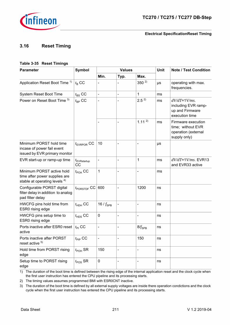
TC270 / TC275 / TC277 DB-Step
Electrical SpecificationReset Timing
Data Sheet 211 V 1.2 2019-04
3.16 Reset Timing
Table 3-35 Reset TimingsParameter Symbol Values Unit Note / Test Condition
Min. Typ. Max.Application Reset Boot Time 1)
1) The duration of the boot time is defined between the rising edge of the internal application reset and the clock cycle when the first user instruction has entered the CPU pipeline and its processing starts.
tB CC - - 350 2)
2) The timing values assumes programmed BMI with ESR0CNT inactive.
µs operating with max. frequencies.
System Reset Boot Time tBS CC - - 1 msPower on Reset Boot Time 3)
3) The duration of the boot time is defined by all external supply voltages are inside there operation condictions and the clock cycle when the first user instruction has entered the CPU pipeline and its processing starts.
tBP CC - - 2.5 2) ms dV/dT=1V/ms. including EVR ramp-up and Firmware execution time
- - 1.11 2) ms Firmware execution time; without EVR operation (external supply only)
Minimum PORST hold time incase of power fail event issued by EVR primary monitor
tEVRPOR CC 10 - - µs
EVR start-up or ramp-up time tEVRstartup CC
- - 1 ms dV/dT=1V/ms. EVR13 and EVR33 active
Minimum PORST active hold time after power supplies are stable at operating levels 4)
tPOA CC 1 - - ms
Configurable PORST digital filter delay in addition to analog pad filter delay
tPORSTDF CC 600 - 1200 ns
HWCFG pins hold time from ESR0 rising edge
tHDH CC 16 / fSPB - - ns
HWCFG pins setup time to ESR0 rising edge
tHDS CC 0 - - ns
Ports inactive after ESR0 reset active
tPI CC - - 8/fSPB ns
Ports inactive after PORST reset active 5)
tPIP CC - - 150 ns
Hold time from PORST rising edge
tPOH SR 150 - - ns
Setup time to PORST rising edge
tPOS SR 0 - - ns

TC270 / TC275 / TC277 DB-Step
Electrical SpecificationReset Timing
Data Sheet 212 V 1.2 2019-04
Figure 3-7 Power, Pad and Reset Timing
4) The regulator that supplies VEXT should ensure that VEXT is in the operational region before PORST is externally released by the regulator. Incase of 5V nominal supply, it should be ensured that VEXT > 4V before PORST is released. Incase of 3.3V nominal supply , it should be ensured that VEXT > 3V before PORST is released. The additional minimum PORST hold time is required as an additional mechanism to avoid consecutive PORST toggling owing to slow supply slopes or residual supply ramp-ups. It is also required to activate external PORST atleast 100us before power-fail is recognised to avoid consecutive PORST toggling on a power fail event.
5) This parameter includes the delay of the analog spike filter in the PORST pad.
reset_beh_aurix
VDDP
PORST
PadsPad-state
undefined
VDD
VDDPPA VDDPPA
Pad-state
undefined
VDDPR
Programmed Z / HTristate Z / pullup H
tPOAtPOA
HWCFG
ESR0
tP IP
Z / H
Cold Warm
t HDH
TESTMODE
t P OS t P OH
t P OS tPOHTRST
t PI
Programmed Programmed
tP I
power -on config
t HDA t HDH
config
t HDA t HDH
config

TC270 / TC275 / TC277 DB-Step
Electrical SpecificationEVR
Data Sheet 213 V 1.2 2019-04
3.17 EVR
Table 3-36 3.3VParameter Symbol Values Unit Note / Test Condition
Min. Typ. Max.Input voltage range 1)
1) A maximum pass device dropout voltage of 700mV is included in the minimum input voltage to ensure optimal pass device operation.
VIN SR 4 - 5.50 V pass device=on chipOutput voltage operational range including load/line regulation and aging incase of LDO regulator
VOUT CC 2.97 3.3 3.63 V pass device=on chip
Output VDDx3 static voltage accuracy after trimming and aging without dynamic load/line Regulation incase of LDO regulator.
VOUTT CC 3.225 3.3 3.375 V pass device=on chip
Output buffer capacitance on VOUT 2)
2) It is recommended to select a capacitor with ESR less than 50 mOhm (0.5MHz - 10 MHz). It is also recommended that the resistance of the supply trace from the pin to the EVR output capacitor is less than 100 mOhm.
COUT CC - 1 - µF pass device=on chip
Primary Undervoltage Reset threshold for VDDx3 3)
3) The reset release on supply ramp-up is delayed by a time duration 20-40 us after reaching undervoltage reset threshold. This serves as a time hysteresis to avoid multiple consecutive cold PORST events during slow supply ramp-ups owing to voltage drop/current jumps when reset is released. The reset limit of 2,97V at pin is for the case with 3.3V generated internally from EVR33. In case the 3.3V supply is provided externally, the bondwire drop will cause a reset at a higher voltage of 3.0V at the VDDP3 pin.
VRST33 CC - - 3.0 V by reset release before EVR trimming on supply ramp-up.
Startup time tSTR CC - - 1000 µs Only EVR33 active. ; pass device=on chip
External VIN supply ramp 4)
4) EVR robust against residual voltage ramp-up starting between 0-1 V.
dVin/dT SR
- 1 50 V/ms pass device=on chip
Load step response dVout/dIout CC
- - 240 mV dI=-70mA/20ns; Tsettle=20us; pass device=on chip
-240 - - mV dI=50mA/20ns; Tsettle=100us; pass device=on chip
Line step response dVout/dVin CC
-20 - 20 mV dV/dT=1V/ms; pass device=on chip

TC270 / TC275 / TC277 DB-Step
Electrical SpecificationEVR
Data Sheet 214 V 1.2 2019-04
Table 3-37 1.3VParameter Symbol Values Unit Note / Test Condition
Min. Typ. Max.Input voltage range 1)
1) A maximum pass device dropout voltage of 700mV is included in the minimum input voltage to ensure optimal pass device operation.
VIN SR 2.97 - 5.5 V pass device=off chipOutput voltage operational range including load/line regulation and aging incase of LDO regulator
VOUT CC 1.17 1.3 1.43 V pass device=off chip
Output VDD static voltage accuracy after trimming without dynamic load/line regulation with aging incase of LDO regulator.
VOUTT CC 1.275 1.3 1.325 V pass device=off chip
Output buffer capacitance on VOUT 2)
2) It is recommended to select a capacitor with ESR less than 50 mOhm (0.5MHz - 10 MHz). It is also recommended that the resistance of the supply trace from the pin to the EVR output capacitor is less than 100 mOhm.
COUT CC 3 4.7 6.3 µF pass device=off chip
Primary undervoltage reset threshold for VDD 3)
3) The reset release on supply ramp-up is delayed by a time duration 30-60 µs after reaching undervoltage reset threshold. This serves as a time hysteresis to avoid multiple consecutive cold PORST events during slow supply ramp-ups owing to voltage drop/current jumps when reset is released.
VRST13 CC - - 1.17 V by reset release before EVR trimming on supply ramp-up. pass device=off chip
Startup time tSTR CC - - 1000 µs pass device=off chip. Only EVR13 active.
External VIN supply ramp 4)
4) EVR robust against residual voltage ramp-up starting between 0-1 V.
dVin/dT SR
- 1 50 V/ms pass device=off chip
Load step response dVout/dIout CC
- - 100 mV dI=-150mA; Tsettle=20µs; pass device=off chip
-100 - - mV dI=100mA; Tsettle=20µs; pass device=off chip
Line step response dVout/dVin CC
-10 - 10 mV dV/dT=1V/ms; pass device=off chip

TC270 / TC275 / TC277 DB-Step
Electrical SpecificationEVR
Data Sheet 215 V 1.2 2019-04
Table 3-38 Supply MonitoringParameter Symbol Values Unit Note / Test Condition
Min. Typ. Max.VEXT primary undervoltage monitor accuracy after trimming 1)
1) The monitor tolerances constitute the inherent variation of the bandgap and ADC over process, voltage and temperature operational ranges. The xxxPRIUV parameters are device individually tested in production with ±1% tolerance about the min and max xxxPRIUV limits.
VEXTPRIUV SR
2.86 2.92 2.97 V VEXT = Undervoltage Reset Threshold
VDDP3 primary undervoltage monitor accuracy after trimming 1)
VDDP3PRIUV SR
2.86 2.90 2.97 V VDDP3 = Undervoltage Reset Threshold
VDD primary undervoltage monitor accuracy after trimming 1)
VDDPRIUV SR
1.13 1.15 1.17 V VDD = Undervoltage Reset Threshold
VEXT secondary supply monitor accuracy
VEXTMON CC 4.9 5.0 5.1 V SWDxxVAL VEXT monitoring threshold=5V=DBh
VDDP3 secondary supply monitor accuracy
VDDP3MON CC
3.23 3.30 3.37 V EVR33xxVAL VDDP3 monitoring threshold=3.3V=91h
VDD secondary supply monitor accuracy
VDDMON CC 1.27 1.30 1.33 V EVR13xxVAL VDD monitoring threshold=1.3V=E4h
EVR primary and secondary monitor measurement latency for a new supply value
tEVRMON CC - - 1.8 µs after trimming
Table 3-39 EVR13 SMPS External componentsParameter Symbol Values Unit Note / Test Condition
Min. Typ. Max.External output capacitor value 1)
COUTDC SR 15.4 22 29.7 µF IDDDC=1A6.5 10 13.5 µF IDDDC=400mA
External output capacitor ESR CDC_ESR SR - - 50 mOhm f≥0.5MHz ; f≤10MHz- - 100 Ohm f=10Hz
External input capacitor value 1) CIN SR 6.5 10 13.5 µF IDDDC=1A4.42 6.8 9.18 µF IDDDC=400mA
External input capacitor ESR CIN_ESR SR - - 50 mOhm f≥0.5MHz ; f≤10MHz- - 100 Ohm f=100Hz
External inductor value 2) LDC SR 2.31 3.3 4.29 µH fDCDC=1.5MHz3.29 4.7 6.11 µH fDCDC=1MHz
External inductor ESR LDC_ESR SR - - 0.2 OhmP + N-channel MOSFET logic level
VLL SR - - 2.5 V

TC270 / TC275 / TC277 DB-Step
Electrical SpecificationEVR
Data Sheet 216 V 1.2 2019-04
P + N-channel MOSFET drain source breakdown voltage
|VBR_DS| SR - - 7 V
P + N-channel MOSFET drain source ON-state resistance
RON SR - - 150 mOhm IDDDC=1A;VGS=2.5V ; TA=25°C
- - 200 mOhm IDDDC=400mA;VGS=2.5V ; TA=25°C
P + N-channel MOSFET Gate Charge
Qac SR - 4 - nC IDDDC=1A; MOS-VGS=5V
- 8 - nC IDDDC=400mA; MOS-VGS=5V
External MOSFET commutation time
tc SR 10 30 40 ns configurable
N-channel MOSFET reverse diode forward voltage
VRDN SR - 0.8 - V
1) Capacitor min-max range represent typical ±35% tolerance including DC bias effect. The trace resistance from the capacitor to the supply or ground rail should be limited to 25 mOhm.
2) External inductor min-max range represent typical ±30% tolerance at a DC bias current of 100mA.
Table 3-40 EVR13 SMPSParameter Symbol Values Unit Note / Test Condition
Min. Typ. Max.Input VEXT Voltage range VIN SR 2.97 - 5.5 VSMPS regulator output voltage range including load/line regulation and aging 1)
VDDDC CC 1.17 - 1.43 V VDD≥2.97V ; VDD≤5.5V ; IDDDC≥1mA ; IDDDC≤1A
SMPS regulator static voltage output accuracy after trimming without dynamic load/line Regulation with aging. 2)
VDDDCT CC 1.275 1.3 1.325 V VDD≥2.97V ; VDD≤5.5V ; IDDDC≥1mA ; IDDDC≤1A
Programmable switching frequency
fDCDC CC 0.4 - 2.0 MHz
Switching frequency modulation spread
ΔfDCSPR CC - - 2% MHz
Maximum ripple at IMAX (peak-to-peak) 3)
ΔVDDDC CC - - 15 mV VDD≥2.97V ; VDD≤5.5V ; IDDDC≥300mA ; IDDDC≤1A
No load current consumption of SMPS regulator
IDCNL CC - 5 10 mA fDCDC=1MHz
Table 3-39 EVR13 SMPS External components (cont’d)Parameter Symbol Values Unit Note / Test Condition
Min. Typ. Max.
TC270 / TC275 / TC277 DB-Step
Electrical SpecificationEVR
Data Sheet 217 V 1.2 2019-04
SMPS regulator load transient response
dVout/dIout CC
-25 - 25 mV dI < 200mA ; fDCDC=1MHz; tr=0.1µs; tf=0.1µs; VDDDC=1.3V
-65 - 65 mV dI < 400mA ; fDCDC=1MHz; tr=0.1µs; tf=0.1µs; VDDDC=1.3V
-130 - 130 mV dI < 700mA ; fDCDC=1MHz; tr=0.1µs; tf=0.1µs; VDDDC=1.3V
Maximum output current of the regulator
IMAX SR - - 1 A limited by thermal constraints and component choice
SMPS regulator efficiency nDC CC - 85 - % VIN=3.3V; IDDDC=300mA; fDCDC=1MHz
- 75 - % VIN=5V; IDDDC=400mA; fDCDC=1.5MHz
- 80 - % VIN=5V; IDDDC=400mA; fDCDC=1MHz
1) Incase of SMPS mode, It shall be ensured that the VDD output pin shall be connected on PCB level to all other VDD Input pins.
2) Incase of fSRI running with max frequency, it shall be ensured that the VDD operating range is limited to 1.235V upto 1.430V. The DCDC may be configured in this case with a nominal voltage of 1.33V±7.5%. The static accuracy and regulation parameter ranges remain also valid for this case.
3) If frequency spreading (SDFREQSPRD = 1) is activated, an additional ripple of 1% need to be considered.
Table 3-40 EVR13 SMPS (cont’d)Parameter Symbol Values Unit Note / Test Condition
Min. Typ. Max.

TC270 / TC275 / TC277 DB-Step
Electrical SpecificationPhase Locked Loop (PLL)
Data Sheet 218 V 1.2 2019-04
3.18 Phase Locked Loop (PLL)
Note: The specified PLL jitter values are valid if the capacitive load per pin does not exceed CL = 20 pF with the maximum driver and sharp edge.
Note: The maximum peak-to-peak noise on the power supply voltage, is limited to a peak-to-peak voltage of VPP = 100 mV for noise frequencies below 300 KHz and VPP = 40 mV for noise frequencies above 300 KHz.These conditions can be achieved by appropriate blocking of the supply voltage as near as possible to the supply pins and using PCB supply and ground planes.
Table 3-41 PLLParameter Symbol Values Unit Note / Test Condition
Min. Typ. Max.PLL base frequency fPLLBASE CC 80 150 360 MHzVCO frequency range fVCO SR 400 - 800 MHzVCO Input frequency range fREF CC 8 - 24 MHzModulation Amplitude MA CC 0 - 2 %Peak Period jitter DP CC -200 - 200 psPeak Accumulated Jitter DPP CC -5 - 5 ns without modulationTotal long term jitter JTOT CC - - 11.5 ns including modulation;
MA ≤ 1%System frequency deviation fSYSD CC - - 0.01 % with active modulationModulation variation frequency fMV CC 2 3.6 5.4 MHzPLL lock-in time tL CC 11.5 - 200 µs

TC270 / TC275 / TC277 DB-Step
Electrical SpecificationERAY Phase Locked Loop (ERAY_PLL)
Data Sheet 219 V 1.2 2019-04
3.19 ERAY Phase Locked Loop (ERAY_PLL)
Note: The specified PLL jitter values are valid if the capacitive load per pin does not exceed CL = 20 pF with the maximum driver and sharp edge.
Note: The maximum peak-to-peak noise on the power supply voltage, is limited to a peak-to-peak voltage of VPP = 100 mV for noise frequencies below 300 KHz and VPP = 40 mV for noise frequencies above 300 KHz.These conditions can be achieved by appropriate blocking of the supply voltage as near as possible to the supply pins and using PCB supply and ground planes.
Table 3-42 PLL_ERAYParameter Symbol Values Unit Note / Test Condition
Min. Typ. Max.PLL Base Frequency of the ERAY PLL
fPLLBASE_ERA
Y CC50 200 320 MHz
VCO frequency range of the ERAY PLL
fVCO_ERAY SR
400 - 480 MHz
VCO input frequency of the ERAY PLL
fREF SR 16 - 24 MHz
Accumulated_Jitter DP CC -0.5 - 0.5 nsAccumulated jitter at SYSCLK pin
DPP CC -0.8 - 0.8 ns
PLL lock-in time tL CC 5.6 - 200 µs

TC270 / TC275 / TC277 DB-Step
Electrical SpecificationAC Specifications
Data Sheet 220 V 1.2 2019-04
3.20 AC SpecificationsAll AC parameters are specified for the complette operating range defined in Chapter 3.4 unless otherwise notedin colum Note / test Condition.
Unless otherwise noted in the figures the timings are defined with the following guidelines:
Figure 3-8 Definition of rise / fall times
Figure 3-9 Time Reference Point Definition
10%
90%
10%
90%
VSS
VEXT/FLEX / VDDP3
tr
rise_fall
tf
timing_reference
VEXT/FLEX /VDDP3Timing
Reference Points
VEXT /FLEX / VDDP3
VSS
VEXT/FLEX / VDDP3
2 2

TC270 / TC275 / TC277 DB-Step
Electrical SpecificationJTAG Parameters
Data Sheet 221 V 1.2 2019-04
3.21 JTAG ParametersThe following parameters are applicable for communication through the JTAG debug interface. The JTAG moduleis fully compliant with IEEE1149.1-2000.
Figure 3-10 Test Clock Timing (TCK)
Table 3-43 JTAGParameter Symbol Values Unit Note / Test Condition
Min. Typ. Max.TCK clock period t1 SR 25 - - nsTCK high time t2 SR 10 - - nsTCK low time t3 SR 10 - - nsTCK clock rise time t4 SR - - 4 nsTCK clock fall time t5 SR - - 4 nsTDI/TMS setup to TCK rising edge
t6 SR 6.0 - - ns
TDI/TMS hold after TCK rising edge
t7 SR 6.0 - - ns
TDO valid after TCK falling edge (propagation delay) 1)
1) The falling edge on TCK is used to generate the TDO timing.
t8 CC 3.0 - - ns CL≤20pF- - 16 ns CL≤50pF
TDO hold after TCK falling edge 1)
t18 CC 2 - - ns
TDO high impedance to valid from TCK falling edge 1)2)
2) The setup time for TDO is given implicitly by the TCK cycle time.
t9 CC - - 17.5 ns CL≤50pF
TDO valid output to high impedance from TCK falling edge 1)
t10 CC - - 17 ns CL≤50pF
MC_JTAG_TCK
0.9 VDDP0.5 VDDP
t1
t2 t3
0.1 VDDPt5 t4

TC270 / TC275 / TC277 DB-Step
Electrical SpecificationJTAG Parameters
Data Sheet 222 V 1.2 2019-04
Figure 3-11 JTAG Timing
t6 t7
t6 t7
t9 t8 t10
TCK
TMS
TDI
TDO
MC_JTAGt18
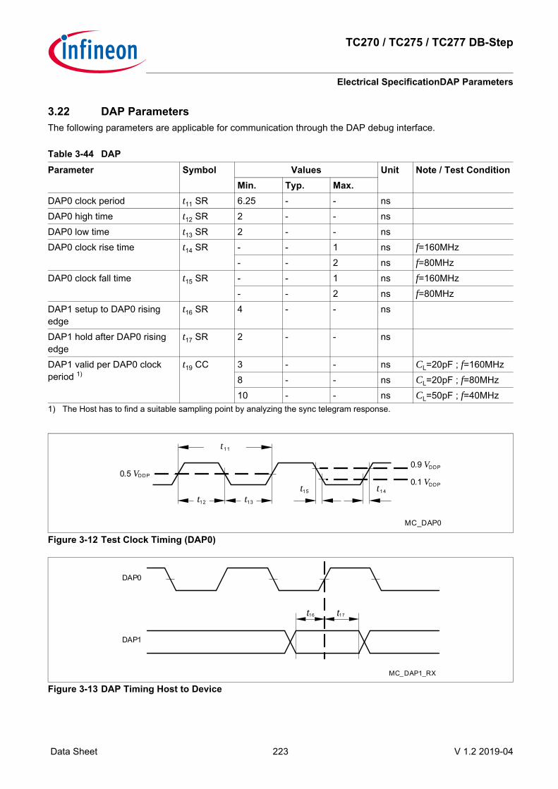
TC270 / TC275 / TC277 DB-Step
Electrical SpecificationDAP Parameters
Data Sheet 223 V 1.2 2019-04
3.22 DAP ParametersThe following parameters are applicable for communication through the DAP debug interface.
Figure 3-12 Test Clock Timing (DAP0)
Figure 3-13 DAP Timing Host to Device
Table 3-44 DAPParameter Symbol Values Unit Note / Test Condition
Min. Typ. Max.DAP0 clock period t11 SR 6.25 - - nsDAP0 high time t12 SR 2 - - nsDAP0 low time t13 SR 2 - - nsDAP0 clock rise time t14 SR - - 1 ns f=160MHz
- - 2 ns f=80MHzDAP0 clock fall time t15 SR - - 1 ns f=160MHz
- - 2 ns f=80MHzDAP1 setup to DAP0 rising edge
t16 SR 4 - - ns
DAP1 hold after DAP0 rising edge
t17 SR 2 - - ns
DAP1 valid per DAP0 clock period 1)
1) The Host has to find a suitable sampling point by analyzing the sync telegram response.
t19 CC 3 - - ns CL=20pF ; f=160MHz8 - - ns CL=20pF ; f=80MHz10 - - ns CL=50pF ; f=40MHz
MC_DAP0
0.9 VDDP0.5 VDDP
t11
t12 t13
0.1 VDDPt15 t14
t16 t17
DAP0
DAP1
MC_DAP1_RX

TC270 / TC275 / TC277 DB-Step
Electrical SpecificationDAP Parameters
Data Sheet 224 V 1.2 2019-04
Figure 3-14 DAP Timing Device to Host (DAP1 and DAP2 pins)
Note: The DAP1 and DAP2 device to host timing is individual for both pins. There is no guaranteed max. signal skew.
DAP1
MC_DAP1_TX
t11
t19

TC270 / TC275 / TC277 DB-Step
Electrical SpecificationASCLIN SPI Master Timing
Data Sheet 225 V 1.2 2019-04
3.23 ASCLIN SPI Master TimingThis section defines the timings for the ASCLIN in the TC270 / TC275 / TC277, for 5V power supply.Note: Pad asymmetry is already included in the following timings.
Table 3-45 Master Mode MP+ss/MPRss output padsParameter Symbol Values Unit Note / Test Condition
Min. Typ. Max.ASCLKO clock period 1)
1) PLL Jitter not included. Should be considered additionally, corresponding to the used baudrate. The duty cycle can be adjusted using the BITCON.SAMPLEPOINT bitfield with the finest granularity of TMAX = 1 / fMAX.
t50 CC 20 - - ns CL=25pFDeviation from ideal duty cycle 2)
2) Positive deviation lenghtens the high time and shortens the low time of a clock period. Negative deviation does the opposite.
t500 CC -3 - 3 ns 0 < CL < 50pF
MTSR delay from ASCLKO shifting edge
t51 CC -7 - 6 ns CL=25pF
ASLSOn delay from the first ASCLKO edge
t510 CC 5 - 35 ns CL=25pF; pad used = LPm
MRST setup to ASCLKO latching edge
t52 SR 28 - - ns CL=25pF
MRST hold from ASCLKO latching edge
t53 SR -6 - - ns CL=25pF
Table 3-46 Master Mode MP+sm/MPRsm output padsParameter Symbol Values Unit Note / Test Condition
Min. Typ. Max.ASCLKO clock period 1)
1) PLL Jitter not included. Should be considered additionally, corresponding to the used baudrate. The duty cycle can be adjusted using the BITCON.SAMPLEPOINT bitfield with the finest granularity of TMAX = 1 / fMAX.
t50 CC 50 - - ns CL=50pFDeviation from ideal duty cycle 2)
2) Positive deviation lenghtens the high time and shortens the low time of a clock period. Negative deviation does the opposite.
t500 CC -2 - 3+0.01 * CL
ns 0 < CL < 200pF
MTSR delay from ASCLKO shifting edge
t51 CC -10 - 10 ns CL=50pF
ASLSOn delay from the first ASCLKO edge
t510 CC 5 - 35 ns CL=50pF; pad used = LPm
MRST setup to ASCLKO latching edge
t52 SR 50 - - ns CL=50pF
MRST hold from ASCLKO latching edge
t53 SR -10 - - ns CL=50pF

TC270 / TC275 / TC277 DB-Step
Electrical SpecificationASCLIN SPI Master Timing
Data Sheet 226 V 1.2 2019-04
Table 3-47 Master Mode MPss output padsParameter Symbol Values Unit Note / Test Condition
Min. Typ. Max.ASCLKO clock period 1)
1) PLL Jitter not included. Should be considered additionally, corresponding to the used baudrate. The duty cycle can be adjusted using the BITCON.SAMPLEPOINT bitfield with the finest granularity of TMAX = 1 / fMAX.
t50 CC 20 - - ns CL=25pFDeviation from ideal duty cycle 2)
2) Positive deviation lenghtens the high time and shortens the low time of a clock period. Negative deviation does the opposite.
t500 CC -2 - 3.5+0.035 * CL
ns 0 < CL < 200pF
MTSR delay from ASCLKO shifting edge
t51 CC -7 - 6 ns CL=25pF
ASLSOn delay from the first ASCLKO edge
t510 CC -7 - 6 ns CL=25pF
MRST setup to ASCLKO latching edge
t52 SR 30 - - ns CL=25pF, else33 3)
3) Please note that these pins didn't support the hystereses inactive feature.
- - ns CL=25pF, for P14.2, P14.4, and P15.1
MRST hold from ASCLKO latching edge
t53 SR -5 - - ns CL=25pF
Table 3-48 Master Mode MPsm output padsParameter Symbol Values Unit Note / Test Condition
Min. Typ. Max.ASCLKO clock period 1)
1) PLL Jitter not included. Should be considered additionally, corresponding to the used baudrate. The duty cycle can be adjusted using the BITCON.SAMPLEPOINT bitfield with the finest granularity of TMAX = 1 / fMAX.
t50 CC 100 - - ns CL=50pFDeviation from ideal duty cycle 2)
2) Positive deviation lenghtens the high time and shortens the low time of a clock period. Negative deviation does the opposite.
t500 CC -3 - 4+0.04 * CL
ns 0 < CL < 200pF
MTSR delay from ASCLKO shifting edge
t51 CC -11 - 10 ns CL=50pF
ASLSOn delay from the first ASCLKO edge
t510 CC -11 - 10 ns CL=50pF
MRST setup to ASCLKO latching edge
t52 SR 60 - - ns CL=50pF
MRST hold from ASCLKO latching edge
t53 SR -10 - - ns CL=50pF

TC270 / TC275 / TC277 DB-Step
Electrical SpecificationASCLIN SPI Master Timing
Data Sheet 227 V 1.2 2019-04
Table 3-49 Master Mode medium output padsParameter Symbol Values Unit Note / Test Condition
Min. Typ. Max.ASCLKO clock period 1)
1) PLL Jitter not included. Should be considered additionally, corresponding to the used baudrate. The duty cycle can be adjusted using the BITCON.SAMPLEPOINT bitfield with the finest granularity of TMAX = 1 / fMAX.
t50 CC 200 - - ns CL=50pFDeviation from ideal duty cycle 2)
2) Positive deviation lenghtens the high time and shortens the low time of a clock period. Negative deviation does the opposite.
t500 CC -8 - 4+0.04 * CL
ns 0 < CL < 200pF
MTSR delay from ASCLKO shifting edge
t51 CC -20 - 15 ns CL=50pF
ASLSOn delay from the first ASCLKO edge
t510 CC -20 - 20 ns CL=50pF
MRST setup to ASCLKO latching edge
t52 SR 70 - - ns CL=50pF
MRST hold from ASCLKO latching edge
t53 SR -10 - - ns CL=50pF
Table 3-50 Master Mode weak output padsParameter Symbol Values Unit Note / Test Condition
Min. Typ. Max.ASCLKO clock period 1)
1) PLL Jitter not included. Should be considered additionally, corresponding to the used baudrate. The duty cycle can be adjusted using the BITCON.SAMPLEPOINT bitfield with the finest granularity of TMAX = 1 / fMAX.
t50 CC 1000 - - ns CL=50pFDeviation from ideal duty cycle 2)
2) Positive deviation lenghtens the high time and shortens the low time of a clock period. Negative deviation does the opposite.
t500 CC -30 - 30+0.15 * CL
ns 0 < CL < 200pF
MTSR delay from ASCLKO shifting edge
t51 CC -75 - 75 ns CL=50pF
ASLSOn delay from the first ASCLKO edge
t510 CC -65 - 65 ns CL=50pF
MRST setup to ASCLKO latching edge
t52 SR 510 - - ns CL=50pF
MRST hold from ASCLKO latching edge
t53 SR -50 - - ns CL=50pF

TC270 / TC275 / TC277 DB-Step
Electrical SpecificationASCLIN SPI Master Timing
Data Sheet 228 V 1.2 2019-04
Figure 3-15 ASCLIN SPI Master Timing
ASCLIN_TmgMM.vsd
ASCLKO
MTSR
t51 t51
MRST
t53
Data valid
ASLSO
t510
t50
t500
t52
Data valid

TC270 / TC275 / TC277 DB-Step
Electrical SpecificationASCLIN SPI Master Timing
Data Sheet 229 V 1.2 2019-04
3.24 ASCLIN SPI Master TimingThis section defines the timings for the ASCLIN in the TC270 / TC275 / TC277, for 3.3V power supply, MediumPerformance pads, strong sharp edge (MPss), CL=25pF.Note: Pad asymmetry is already included in the following timings.
Table 3-51 Master Mode MP+ss/MPRss output padsParameter Symbol Values Unit Note / Test Condition
Min. Typ. Max.ASCLKO clock period 1)
1) PLL Jitter not included. Should be considered additionally, corresponding to the used baudrate. The duty cycle can be adjusted using the BITCON.SAMPLEPOINT bitfield with the finest granularity of TMAX = 1 / fMAX.
t50 CC 40 - - ns CL=25pFDeviation from ideal duty cycle 2)
2) Positive deviation lenghtens the high time and shortens the low time of a clock period. Negative deviation does the opposite.
t500 CC -5 - 5 ns 0 < CL < 50pF
MTSR delay from ASCLKO shifting edge
t51 CC -12 - 12 ns CL=25pF
ASLSOn delay from the first ASCLKO edge
t510 CC 0 - 60 ns CL=25pF; pad used = LPm
MRST setup to ASCLKO latching edge
t52 SR 50 - - ns CL=25pF
MRST hold from ASCLKO latching edge
t53 SR -5 - - ns CL=25pF
Table 3-52 Master Mode MP+sm/MPRsm output padsParameter Symbol Values Unit Note / Test Condition
Min. Typ. Max.ASCLKO clock period 1)
1) PLL Jitter not included. Should be considered additionally, corresponding to the used baudrate. The duty cycle can be adjusted using the BITCON.SAMPLEPOINT bitfield with the finest granularity of TMAX = 1 / fMAX.
t50 CC 100 - - ns CL=50pFDeviation from ideal duty cycle 2)
2) Positive deviation lenghtens the high time and shortens the low time of a clock period. Negative deviation does the opposite.
t500 CC -3 - 7 ns 0 < CL < 200pF
MTSR delay from ASCLKO shifting edge
t51 CC -17 - 17 ns CL=50pF
ASLSOn delay from the first ASCLKO edge
t510 CC 0 - 60 ns CL=50pF; pad used = LPm
MRST setup to ASCLKO latching edge
t52 SR 85 - - ns CL=50pF
MRST hold from ASCLKO latching edge
t53 SR -5 - - ns CL=50pF

TC270 / TC275 / TC277 DB-Step
Electrical SpecificationASCLIN SPI Master Timing
Data Sheet 230 V 1.2 2019-04
Table 3-53 Master Mode MPss output padsParameter Symbol Values Unit Note / Test Condition
Min. Typ. Max.ASCLKO clock period 1)
1) PLL Jitter not included. Should be considered additionally, corresponding to the used baudrate. The duty cycle can be adjusted using the BITCON.SAMPLEPOINT bitfield with the finest granularity of TMAX = 1 / fMAX.
t50 CC 40 - - ns CL=25pFDeviation from ideal duty cycle 2)
2) Positive deviation lenghtens the high time and shortens the low time of a clock period. Negative deviation does the opposite.
t500 CC -5 - 7+0.07 * CL
ns 0 < CL < 200pF
MTSR delay from ASCLKO shifting edge
t51 CC -12 - 12 ns CL=25pF
ASLSOn delay from the first ASCLKO edge
t510 CC -12 - 12 ns CL=25pF
MRST setup to ASCLKO latching edge
t52 SR 50 - - ns CL=25pF
MRST hold from ASCLKO latching edge
t53 SR -5 - - ns CL=25pF
Table 3-54 Master Mode MPsm output padsParameter Symbol Values Unit Note / Test Condition
Min. Typ. Max.ASCLKO clock period 1)
1) PLL Jitter not included. Should be considered additionally, corresponding to the used baudrate. The duty cycle can be adjusted using the BITCON.SAMPLEPOINT bitfield with the finest granularity of TMAX = 1 / fMAX.
t50 CC 200 - - ns CL=50pFDeviation from ideal duty cycle 2)
2) Positive deviation lenghtens the high time and shortens the low time of a clock period. Negative deviation does the opposite.
t500 CC -5 - 9+0.06 * CL
ns 0 < CL < 200pF
MTSR delay from ASCLKO shifting edge
t51 CC -19 - 17 ns CL=50pF
ASLSOn delay from the first ASCLKO edge
t510 CC -19 - 17 ns CL=50pF
MRST setup to ASCLKO latching edge
t52 SR 100 - - ns CL=50pF
MRST hold from ASCLKO latching edge
t53 SR -13 - - ns CL=50pF
Table 3-55 Master Mode medium output padsParameter Symbol Values Unit Note / Test Condition
Min. Typ. Max.ASCLKO clock period 1) t50 CC 400 - - ns CL=50pFDeviation from ideal duty cycle 2)
t500 CC -6-0.07 * CL
- 6+0.07 * CL
ns 0 < CL < 200pF

TC270 / TC275 / TC277 DB-Step
Electrical SpecificationASCLIN SPI Master Timing
Data Sheet 231 V 1.2 2019-04
MTSR delay from ASCLKO shifting edge
t51 CC -33 - 25 ns CL=50pF
ASLSOn delay from the first ASCLKO edge
t510 CC -35 - 35 ns CL=50pF
MRST setup to ASCLKO latching edge
t52 SR 120 - - ns CL=50pF
MRST hold from ASCLKO latching edge
t53 SR -13 - - ns CL=50pF
1) PLL Jitter not included. Should be considered additionally, corresponding to the used baudrate. The duty cycle can be adjusted using the BITCON.SAMPLEPOINT bitfield with the finest granularity of TMAX = 1 / fMAX.
2) Positive deviation lenghtens the high time and shortens the low time of a clock period. Negative deviation does the opposite.
Table 3-56 Master Mode weak output padsParameter Symbol Values Unit Note / Test Condition
Min. Typ. Max.ASCLKO clock period 1)
1) PLL Jitter not included. Should be considered additionally, corresponding to the used baudrate. The duty cycle can be adjusted using the BITCON.SAMPLEPOINT bitfield with the finest granularity of TMAX = 1 / fMAX.
t50 CC 2000 - - ns CL=50pFDeviation from ideal duty cycle 2)
2) Positive deviation lenghtens the high time and shortens the low time of a clock period. Negative deviation does the opposite.
t500 CC -110 - 150 ns 0 < CL < 200pF
MTSR delay from ASCLKO shifting edge
t51 CC -170 - 170 ns CL=50pF
ASLSOn delay from the first ASCLKO edge
t510 CC -170 - 170 ns CL=50pF
MRST setup to ASCLKO latching edge
t52 SR 510 - - ns CL=50pF
MRST hold from ASCLKO latching edge
t53 SR -40 - - ns CL=50pF
Table 3-57 Master Mode A2ss output padsParameter Symbol Values Unit Note / Test Condition
Min. Typ. Max.ASCLKO clock period 1) t50 CC 20 - - ns CL=50pFDeviation from ideal duty cycle 2)
t500 CC -3 - 3 ns CL=50pF
MTSR delay from ASCLKO shifting edge
t51 CC -4 - 4 ns CL=50pF
ASLSOn delay from the first ASCLKO edge
t510 CC -5 - 4 ns CL=50pF
Table 3-55 Master Mode medium output pads (cont’d)Parameter Symbol Values Unit Note / Test Condition
Min. Typ. Max.

TC270 / TC275 / TC277 DB-Step
Electrical SpecificationASCLIN SPI Master Timing
Data Sheet 232 V 1.2 2019-04
Figure 3-16 ASCLIN SPI Master Timing
MRST setup to ASCLKO latching edge
t52 SR 17 - - ns CL=50pF
MRST hold from ASCLKO latching edge
t53 SR 0 - - ns CL=50pF
1) PLL Jitter not included. Should be considered additionally, corresponding to the used baudrate. The duty cycle can be adjusted using the BITCON.SAMPLEPOINT bitfield with the finest granularity of TMAX = 1 / fMAX.
2) Positive deviation lenghtens the high time and shortens the low time of a clock period. Negative deviation does the opposite.
Table 3-58 Master Mode A2sm output padsParameter Symbol Values Unit Note / Test Condition
Min. Typ. Max.ASCLKO clock period 1)
1) PLL Jitter not included. Should be considered additionally, corresponding to the used baudrate. The duty cycle can be adjusted using the BITCON.SAMPLEPOINT bitfield with the finest granularity of TMAX = 1 / fMAX.
t50 CC 40 - - ns CL=50pFDeviation from ideal duty cycle 2)
2) Positive deviation lenghtens the high time and shortens the low time of a clock period. Negative deviation does the opposite.
t500 CC -4 - 4 ns CL=50pF
MTSR delay from ASCLKO shifting edge
t51 CC -8 - 6 ns CL=50pF
ASLSOn delay from the first ASCLKO edge
t510 CC -8 - 9 ns CL=50pF
MRST setup to ASCLKO latching edge
t52 SR 26 - - ns CL=50pF
MRST hold from ASCLKO latching edge
t53 SR 0 - - ns CL=50pF
Table 3-57 Master Mode A2ss output pads (cont’d)Parameter Symbol Values Unit Note / Test Condition
Min. Typ. Max.
ASCLIN_TmgMM.vsd
ASCLKO
MTSR
t51 t51
MRST
t53
Data valid
ASLSO
t510
t50
t500
t52
Data valid

TC270 / TC275 / TC277 DB-Step
Electrical SpecificationQSPI Timings, Master and Slave Mode
Data Sheet 233 V 1.2 2019-04
3.25 QSPI Timings, Master and Slave ModeThis section defines the timings for the QSPI in the TC270 / TC275 / TC277, for 5V pad power supply. It is assumed that SCLKO, MTSR, and SLSO pads have the same pad settings:• LVDSM output pads,LVDSH input pad, master mode, CL=25pF• Medium Performance Plus Pads (MP+):
– strong sharp edge (MP+ss), CL=25pF– strong medium edge (MP+sm), CL=50pF– medium edge (MP+m), CL=50pF– weak edge (MP+w), CL=50pF
• Medium Performance Pads (MP):– strong sharp edge (MPss), CL=25pF– strong medium edge (MPsm), CL=50pF
• Medium and Low Performance Pads (MP/LP), the identical output strength settings:– medium edge (LP/MPm), CL=50pF– weak edge (MPw), CL=50pF
Note: Pad asymmetry is already included in the following timings.
Table 3-59 Master Mode Timing, LVDSM output pads for data and clockParameter Symbol Values Unit Note / Test Condition
Min. Typ. Max.SCLKO clock period 1)
1) Documented value is valid for master transmit or slave receive only. For full duplex the external SPI counterpart timing has to be taken into account.
t50 CC 20 2)
2) The capacitive load on the LVDS pins is differential, the capacitive load on the CMOS pins is single ended.
- - ns CL=25pFDeviation from the ideal duty cycle 3) 4)
3) The PLL jitter is not included. It should be considered additionally, corresponding to the used baudrate. The duty cycle can be adjusted using the bit fields ECONz.A, B and C with the finest granularity of TMAX = 1 / fMAX.
4) Positive deviation lenghtens the high time and shortens the low time of a clock period. Negative deviation does the opposite.
t500 CC -1 - 1 ns CL=25pF
MTSR delay from SCLKO shifting edge
t51 CC -3 - 3 ns CL=25pF
SLSOn deviation from the ideal programmed position
t510 CC 0 - 30 ns CL=25pF; MPsm-5 - 7 ns CL=25pF; MPss-4 - 7 ns MP+ss; CL=25pF-1 - 15 ns MP+sm; CL=25pF
MRST setup to SCLK latching edge 5)
5) For compensation of the average on-chip delay the QSPI module provides the bit fields ECONz.A, B and C.
t52 SR 19 5) - - ns CL=25pF; LVDSM 5V output and LVDSH 3.3V input
MRST hold from SCLK latching edge
t53 SR -6 5) - - ns CL=25pF; LVDSM 5V output and LVDSH 3.3V input

TC270 / TC275 / TC277 DB-Step
Electrical SpecificationQSPI Timings, Master and Slave Mode
Data Sheet 234 V 1.2 2019-04
Table 3-60 Master Mode MP+ss/MPRss output padsParameter Symbol Values Unit Note / Test Condition
Min. Typ. Max.SCLKO clock period 1)
1) Documented value is valid for master transmit or slave receive only. For full duplex the external SPI counterpart timing has to be taken into account.
t50 CC 20 - - ns CL=25pFDeviation from the ideal duty cycle 2) 3)
2) The PLL jitter is not included. It should be considered additionally, corresponding to the used baudrate. The duty cycle can be adjusted using the bit fields ECONz.A, B and C with the finest granularity of TMAX = 1 / fMAX.
3) Positive deviation lenghtens the high time and shortens the low time of a clock period. Negative deviation does the opposite.
t500 CC -3 - 3 ns 0 < CL < 50pF
MTSR delay from SCLKO shifting edge
t51 CC -7 - 6 ns CL=25pF
SLSOn deviation from the ideal programmed position
t510 CC -7 - 6 ns CL=25pF
MRST setup to SCLK latching edge 4)
4) For compensation of the average on-chip delay the QSPI module provides the bit fields ECONz.A, B and C.
t52 SR 27 4)5)
5) The setup and hold times are valid for both settings of the input pads thresholds: TTL and AL.
- - ns CL=25pF
MRST hold from SCLK latching edge
t53 SR -6 4)5) - - ns CL=25pF
Table 3-61 Master Mode MP+sm/MPRsm output pads for data and clockParameter Symbol Values Unit Note / Test Condition
Min. Typ. Max.SCLKO clock period 1)
1) Documented value is valid for master transmit or slave receive only. For full duplex the external SPI counterpart timing has to be taken into account.
t50 CC 50 - - ns CL=50pFDeviation from the ideal duty cycle 2) 3)
2) The PLL jitter is not included. It should be considered additionally, corresponding to the used baudrate. The duty cycle can be adjusted using the bit fields ECONz.A, B and C with the finest granularity of TMAX = 1 / fMAX.
3) Positive deviation lenghtens the high time and shortens the low time of a clock period. Negative deviation does the opposite.
t500 CC -2 - 3+0.01 * CL
ns 0 < CL < 200pF
MTSR delay from SCLKO shifting edge
t51 CC -10 - 10 ns CL=50pF
SLSOn deviation from the ideal programmed position
t510 CC -10 - 10 ns MP+sm; CL=50pF-13 - 1 ns MPss; CL=50pF0 - 40 ns MP+m, MPm, LPm;
CL=50pFMRST setup to SCLK latching edge 4)
t52 SR 50 4)5) - - ns CL=50pF
MRST hold from SCLK latching edge
t53 SR -10 4)5) - - ns CL=50pF

TC270 / TC275 / TC277 DB-Step
Electrical SpecificationQSPI Timings, Master and Slave Mode
Data Sheet 235 V 1.2 2019-04
4) For compensation of the average on-chip delay the QSPI module provides the bit fields ECONz.A, B and C.5) The setup and hold times are valid for both settings of the input pads thresholds: TTL and AL.
Table 3-62 Master Mode timing MPsm output padsParameter Symbol Values Unit Note / Test Condition
Min. Typ. Max.SCLKO clock period 1)
1) Documented value is valid for master transmit or slave receive only. For full duplex the external SPI counterpart timing has to be taken into account.
t50 CC 100 - - ns CL=50pFDeviation from the ideal duty cycle 2) 3)
2) The PLL jitter is not included. It should be considered additionally, corresponding to the used baudrate. The duty cycle can be adjusted using the bit fields ECONz.A, B and C with the finest granularity of TMAX = 1 / fMAX.
3) Positive deviation lenghtens the high time and shortens the low time of a clock period. Negative deviation does the opposite.
t500 CC -3 - 4+0.04 * CL
ns 0 < CL < 200pF
MTSR delay from SCLKO shifting edge
t51 CC -11 - 10 ns CL=50pF
SLSOn deviation from the ideal programmed position
t510 CC -11 - 10 ns CL=50pF
MRST setup to SCLK latching edge 4)
4) For compensation of the average on-chip delay the QSPI module provides the bit fields ECONz.A, B and C.
t52 SR 60 4)5)
5) The setup and hold times are valid for both settings of the input pads thresholds: TTL and AL.
- - ns CL=50pF
MRST hold from SCLK latching edge
t53 SR -10 4)5) - - ns CL=50pF
Table 3-63 Master Mode timing MPRm/MP+m/MPm/LPm output padsParameter Symbol Values Unit Note / Test Condition
Min. Typ. Max.SCLKO clock period 1)
1) Documented value is valid for master transmit or slave receive only. For full duplex the external SPI counterpart timing has to be taken into account.
t50 CC 200 - - ns CL=50pFDeviation from the ideal duty cycle 2) 3)
2) The PLL jitter is not included. It should be considered additionally, corresponding to the used baudrate. The duty cycle can be adjusted using the bit fields ECONz.A, B and C with the finest granularity of TMAX = 1 / fMAX.
3) Positive deviation lenghtens the high time and shortens the low time of a clock period. Negative deviation does the opposite.
t500 CC -10 - 10+0.04 * CL
ns 0 < CL < 200pF
MTSR delay from SCLKO shifting edge
t51 CC -15 - 19 ns CL=50pF
SLSOn deviation from the ideal programmed position
t510 CC -20 - 20 ns CL=50pF
MRST setup to SCLK latching edge 4)
t52 SR 70 4)5) - - ns CL=50pF
MRST hold from SCLK latching edge
t53 SR -10 4)5) - - ns CL=50pF

TC270 / TC275 / TC277 DB-Step
Electrical SpecificationQSPI Timings, Master and Slave Mode
Data Sheet 236 V 1.2 2019-04
4) For compensation of the average on-chip delay the QSPI module provides the bit fields ECONz.A, B and C.5) The setup and hold times are valid for both settings of the input pads thresholds: TTL and AL.
Table 3-64 Master Mode Weak output padsParameter Symbol Values Unit Note / Test Condition
Min. Typ. Max.SCLKO clock period 1)
1) Documented value is valid for master transmit or slave receive only. For full duplex the external SPI counterpart timing has to be taken into account.
t50 CC 1000 - - ns CL=50pFDeviation from the ideal duty cycle 2) 3)
2) The PLL jitter is not included. It should be considered additionally, corresponding to the used baudrate. The duty cycle can be adjusted using the bit fields ECONz.A, B and C with the finest granularity of TMAX = 1 / fMAX.
3) Positive deviation lenghtens the high time and shortens the low time of a clock period. Negative deviation does the opposite.
t500 CC -30 - 30+0.15 * CL
ns 0 < CL < 200pF
MTSR delay from SCLKO shifting edge
t51 CC -65 - 65 ns CL=50pF
SLSOn deviation from the ideal programmed position
t510 CC -70 - 65 ns CL=50pF
MRST setup to SCLK latching edge 4)
4) For compensation of the average on-chip delay the QSPI module provides the bit fields ECONz.A, B and C.
t52 SR 300 4)5)
5) The setup and hold times are valid for both settings of the input pads thresholds: TTL and AL.
- - ns CL=50pF
MRST hold from SCLK latching edge
t53 SR -40 4)5) - - ns CL=50pF
Table 3-65 Slave mode timingParameter Symbol Values Unit Note / Test Condition
Min. Typ. Max.SCLK clock period t54 SR 4 x TMAX - - nsSCLK duty cycle t55/t54 SR 40 - 60 %MTSR setup to SCLK latching edge
t56 SR 4 1) - - ns Hystheresis Inactive5 1) - - ns Input Level AL5 1) - - ns Input Level TTL
MTSR hold from SCLK latching edge
t57 SR 3 1) - - ns Hystheresis Inactive6 1) - - ns Input Level AL9 1) - - ns Input Level TTL
SLSI setup to first SCLK shift edge
t58 SR 5 1) - - ns Hystheresis Inactive4 1) - - ns Input Level AL8 1) - - ns Input Level TTL6 - - ns Only for pin 15.1, AL

TC270 / TC275 / TC277 DB-Step
Electrical SpecificationQSPI Timings, Master and Slave Mode
Data Sheet 237 V 1.2 2019-04
Figure 3-17 Master Mode Timing
SLSI hold from last SCLK latching edge
t59 SR 3 1) - - ns Hystheresis Inactive4 1) - - ns Input Level AL8 1) - - ns Input Level TTL
MRST delay from SCLK shift edge
t60 CC 10 - 70 ns MP+m/MPRm; CL=50pF
10 - 50 ns MP+sm/MPRsm; CL=50pF
5 - 30 ns MP+ss/MPRss; CL=25pF
40 - 300 ns MP+w/MPRw; CL=50pF
10 - 70 ns MPm/LPm; CL=50pF10 - 55 ns MPsm; CL=50pF5 - 30 ns MPss; CL=25pF40 - 300 ns MPw/LPw; CL=50pF
SLSI to valid data on MRST t61 SR - - 5 ns1) Except pin P15.1.
Table 3-65 Slave mode timing (cont’d)Parameter Symbol Values Unit Note / Test Condition
Min. Typ. Max.
QSPI_TmgMM.vsd
SCLK1)2)
MTSR1)
t51
MRST1)
t53
Data valid
SLSOn2)
1) This timing is based on the following setup: ECON.CPH = 1, ECON.CPOL = 0, ECON.B=0 (no sampling point delay).
2) t510 is the deviation from the ideal position configured with the leading delay, BACON.LPRE and BACON.LEAD > 0.
t50
t500
t52
Data valid
SAMPLING POINT
t510
0.5 VEXT/FLEX
0.5 VEXT/FLEX
0.5 VEXT/FLEX

TC270 / TC275 / TC277 DB-Step
Electrical SpecificationQSPI Timings, Master and Slave Mode
Data Sheet 238 V 1.2 2019-04
Figure 3-18 Slave Mode Timing
3.26 QSPI Timings, Master and Slave ModeThis section defines the timings for the QSPI in the TC270 / TC275 / TC277, for 3.3V pad power supply. It is assumed that SCLKO, MTSR, and SLSO pads have the same pad settings:• LVDSM output pads, LVDSH input pad, master mode, CL=25pF• Medium Performance Plus Pads (MP+):
– strong sharp edge (MP+ss), CL=25pF– strong medium edge (MP+sm), CL=50pF– medium edge (MP+m), CL=50pF– weak edge (MP+w), CL=50pF
• Medium Performance Pads (MP):– strong sharp edge (MPss), CL=25pF– strong medium edge (MPsm), CL=50pF
• Medium and Low Performance Pads (MP/LP), the identical output strength settings:– medium edge (LP/MPm), CL=50pF– weak edge (MPw), CL=50pF
Note: Pad asymmetry is already included in the following timings.
Table 3-66 Master Mode Timing, LVDSM output pads for data and clockParameter Symbol Values Unit Note / Test Condition
Min. Typ. Max.SCLKO clock period 1) t50 CC 20 - - ns CL=25pFDeviation from the ideal duty cycle 2) 3)
t500 CC -2 - 2 ns CL=25pF
MTSR delay from SCLKO shifting edge
t51 CC -5 - 5 ns CL=25pF
QSPI_TmgSM.vsd
SCLKI1)
t55
MTSR1)
t57
Datavalid
t56
SLSI
1) This timing is based on the following setup: ECON.CPH = 1, ECON.CPOL = 0.
t54
t55
t59
Last latching SCLK edge
First latching SCLK edge
t57
Datavalid
t56
MRST1)
t60
First shift SCLK edge
t60
t61
t580.5 VEXT/FLEX
0.5 VEXT/FLEX

TC270 / TC275 / TC277 DB-Step
Electrical SpecificationQSPI Timings, Master and Slave Mode
Data Sheet 239 V 1.2 2019-04
SLSOn deviation from the ideal programmed position
t510 CC -2 - 55 ns CL=25pF; MPsm-9 - 12 ns CL=25pF; MPss-7 - 12 ns MP+ss; CL=25pF-2 - 26 ns MP+sm; CL=25pF
MRST setup to SCLK latching edge 4)
t52 SR 20 - - ns CL=25pF; LVDSM 5V output and LVDSH 3.3V input
MRST hold from SCLK latching edge
t53 SR -6 - - ns CL=25pF; LVDSM 5V output and LVDSH 3.3V input
1) Documented value is valid for master transmit or slave receive only. For full duplex the external SPI counterpart timing has to be taken into account.
2) The PLL jitter is not included. It should be considered additionally, corresponding to the used baudrate. The duty cycle can be adjusted using the bit fields ECONz.A, B and C with the finest granularity of TMAX = 1 / fMAX.
3) Positive deviation lenghtens the high time and shortens the low time of a clock period. Negative deviation does the opposite.
4) For compensation of the average on-chip delay the QSPI module provides the bit fields ECONz.A, B and C.
Table 3-67 Master Mode MP+ss/MPRss output padsParameter Symbol Values Unit Note / Test Condition
Min. Typ. Max.SCLKO clock period 1)
1) Documented value is valid for master transmit or slave receive only. For full duplex the external SPI counterpart timing has to be taken into account.
t50 CC 40 - - ns CL=25pFDeviation from the ideal duty cycle 2) 3)
2) The PLL jitter is not included. It should be considered additionally, corresponding to the used baudrate. The duty cycle can be adjusted using the bit fields ECONz.A, B and C with the finest granularity of TMAX = 1 / fMAX.
3) Positive deviation lenghtens the high time and shortens the low time of a clock period. Negative deviation does the opposite.
t500 CC -5 - 5 ns 0 < CL < 50pF
MTSR delay from SCLKO shifting edge
t51 CC -12 - 12 ns CL=25pF
SLSOn deviation from the ideal programmed position
t510 CC -12 - 12 ns CL=25pF
MRST setup to SCLK latching edge 4)
4) For compensation of the average on-chip delay the QSPI module provides the bit fields ECONz.A, B and C.
t52 SR 50 4)5)
5) The setup and hold times are valid for both settings of the input pads thresholds: TTL and AL.
- - ns CL=25pF
MRST hold from SCLK latching edge
t53 SR -6 4)5) - - ns CL=25pF
Table 3-66 Master Mode Timing, LVDSM output pads for data and clock (cont’d)Parameter Symbol Values Unit Note / Test Condition
Min. Typ. Max.

TC270 / TC275 / TC277 DB-Step
Electrical SpecificationQSPI Timings, Master and Slave Mode
Data Sheet 240 V 1.2 2019-04
Table 3-68 Master Mode MP+sm/MPRsm output pads for data and clockParameter Symbol Values Unit Note / Test Condition
Min. Typ. Max.SCLKO clock period 1)
1) Documented value is valid for master transmit or slave receive only. For full duplex the external SPI counterpart timing has to be taken into account.
t50 CC 100 - - ns CL=50pFDeviation from the ideal duty cycle 2) 3)
2) The PLL jitter is not included. It should be considered additionally, corresponding to the used baudrate. The duty cycle can be adjusted using the bit fields ECONz.A, B and C with the finest granularity of TMAX = 1 / fMAX.
3) Positive deviation lenghtens the high time and shortens the low time of a clock period. Negative deviation does the opposite.
t500 CC -3 - 7 ns 0 < CL < 200pF
MTSR delay from SCLKO shifting edge
t51 CC -17 - 17 ns CL=50pF
SLSOn deviation from the ideal programmed position
t510 CC -17 - 17 ns MP+sm; CL=50pF-22 - 2 ns MPss; CL=50pF0 - 70 ns MP+m; MPm; LPm;
CL=50pFMRST setup to SCLK latching edge 4)
4) For compensation of the average on-chip delay the QSPI module provides the bit fields ECONz.A, B and C.
t52 SR 85 4)5)
5) The setup and hold times are valid for both settings of the input pads thresholds: TTL and AL.
- - ns CL=50pF
MRST hold from SCLK latching edge
t53 SR -10 4)5) - - ns CL=50pF
Table 3-69 Master Mode timing MPss output padsParameter Symbol Values Unit Note / Test Condition
Min. Typ. Max.SCLKO clock period 1)
1) Documented value is valid for master transmit or slave receive only. For full duplex the external SPI counterpart timing has to be taken into account.
t50 CC 40 - - ns CL=25pFDeviation from the ideal duty cycle 2) 3)
2) The PLL jitter is not included. It should be considered additionally, corresponding to the used baudrate. The duty cycle can be adjusted using the bit fields ECONz.A, B and C with the finest granularity of TMAX = 1 / fMAX.
3) Positive deviation lenghtens the high time and shortens the low time of a clock period. Negative deviation does the opposite.
t500 CC -5 - 7+0.07 * CL
ns CL=25pF
MTSR delay from SCLKO shifting edge
t51 CC -10 - 10 ns CL=25pF
SLSOn deviation from the ideal programmed position
t510 CC -10 - 10 ns CL=25pF
MRST setup to SCLK latching edge 4)
t52 SR 50 4)5) - - ns CL=25pF
MRST hold from SCLK latching edge
t53 SR -6 4)5) - - ns CL=25pF

TC270 / TC275 / TC277 DB-Step
Electrical SpecificationQSPI Timings, Master and Slave Mode
Data Sheet 241 V 1.2 2019-04
4) For compensation of the average on-chip delay the QSPI module provides the bit fields ECONz.A, B and C.5) The setup and hold times are valid for both settings of the input pads thresholds: TTL and AL.
Table 3-70 Master Mode timing MPsm output padsParameter Symbol Values Unit Note / Test Condition
Min. Typ. Max.SCLKO clock period 1)
1) Documented value is valid for master transmit or slave receive only. For full duplex the external SPI counterpart timing has to be taken into account.
t50 CC 200 - - ns CL=50pFDeviation from the ideal duty cycle 2) 3)
2) The PLL jitter is not included. It should be considered additionally, corresponding to the used baudrate. The duty cycle can be adjusted using the bit fields ECONz.A, B and C with the finest granularity of TMAX = 1 / fMAX.
3) Positive deviation lenghtens the high time and shortens the low time of a clock period. Negative deviation does the opposite.
t500 CC -5 - 9+0.06 * CL
ns 0 < CL < 200pF
MTSR delay from SCLKO shifting edge
t51 CC -19 - 19 ns CL=50pF
SLSOn deviation from the ideal programmed position
t510 CC -19 - 17 ns CL=50pF
MRST setup to SCLK latching edge 4)
4) For compensation of the average on-chip delay the QSPI module provides the bit fields ECONz.A, B and C.
t52 SR 100 4)5)
5) The setup and hold times are valid for both settings of the input pads thresholds: TTL and AL.
- - ns CL=50pF
MRST hold from SCLK latching edge
t53 SR -13 4)5) - - ns CL=50pF
Table 3-71 Master Mode timing MPRm/MP+m/MPm/LPm output padsParameter Symbol Values Unit Note / Test Condition
Min. Typ. Max.SCLKO clock period 1)
1) Documented value is valid for master transmit or slave receive only. For full duplex the external SPI counterpart timing has to be taken into account.
t50 CC 400 - - ns CL=50pFDeviation from the ideal duty cycle 2) 3)
2) The PLL jitter is not included. It should be considered additionally, corresponding to the used baudrate. The duty cycle can be adjusted using the bit fields ECONz.A, B and C with the finest granularity of TMAX = 1 / fMAX.
3) Positive deviation lenghtens the high time and shortens the low time of a clock period. Negative deviation does the opposite.
t500 CC -6-0.07 * CL
- 6+0.07 * CL
ns 0 < CL < 200pF
MTSR delay from SCLKO shifting edge
t51 CC -25 - 33 ns CL=50pF
SLSOn deviation from the ideal programmed position
t510 CC -35 - 35 ns CL=50pF
MRST setup to SCLK latching edge 4)
t52 SR 120 4)5) - - ns CL=50pF
MRST hold from SCLK latching edge
t53 SR -13 4)5) - - ns CL=50pF

TC270 / TC275 / TC277 DB-Step
Electrical SpecificationQSPI Timings, Master and Slave Mode
Data Sheet 242 V 1.2 2019-04
4) For compensation of the average on-chip delay the QSPI module provides the bit fields ECONz.A, B and C.5) The setup and hold times are valid for both settings of the input pads thresholds: TTL and AL.
Table 3-72 Master Mode Weak output padsParameter Symbol Values Unit Note / Test Condition
Min. Typ. Max.SCLKO clock period 1)
1) Documented value is valid for master transmit or slave receive only. For full duplex the external SPI counterpart timing has to be taken into account.
t50 CC 2000 - - ns CL=50pFDeviation from the ideal duty cycle 2) 3)
2) The PLL jitter is not included. It should be considered additionally, corresponding to the used baudrate. The duty cycle can be adjusted using the bit fields ECONz.A, B and C with the finest granularity of TMAX = 1 / fMAX.
3) Positive deviation lenghtens the high time and shortens the low time of a clock period. Negative deviation does the opposite.
t500 CC -110 - 110 ns 0 < CL < 200pF
MTSR delay from SCLKO shifting edge
t51 CC -170 - 170 ns CL=50pF
SLSOn deviation from the ideal programmed position
t510 CC -170 - 170 ns CL=50pF
MRST setup to SCLK latching edge 4)
4) For compensation of the average on-chip delay the QSPI module provides the bit fields ECONz.A, B and C.
t52 SR 510 4)5)
5) The setup and hold times are valid for both settings of the input pads thresholds: TTL and AL.
- - ns CL=50pF
MRST hold from SCLK latching edge
t53 SR -40 4)5) - - ns CL=50pF
Table 3-73 Slave mode timingParameter Symbol Values Unit Note / Test Condition
Min. Typ. Max.SCLK clock period t54 SR 4 x TMAX - - nsSCLK duty cycle t55/t54 SR 40 - 60 %MTSR setup to SCLK latching edge
t56 SR 7 1) - - ns Hystheresis inactive9 1) - - ns Input Level AL7 1) - - ns Input Level TTL
MTSR hold from SCLK latching edge
t57 SR 5 1) - - ns Hystheresis inactive11 1) - - ns Input Level AL16 1) - - ns Input Level TTL
SLSI setup to first SCLK shift edge
t58 SR 7 1) - - ns Hystheresis inactive7 1) - - ns Input Level AL14 1) - - ns Input Level TTL11 - - ns Only for pin P15.1, AL

TC270 / TC275 / TC277 DB-Step
Electrical SpecificationQSPI Timings, Master and Slave Mode
Data Sheet 243 V 1.2 2019-04
Figure 3-19 Master Mode Timing
SLSI hold from last SCLK latching edge
t59 SR 5 1) - - ns Hystheresis inactive7 1) - - ns Input Level AL14 1) - - ns Input Level TTL
MRST delay from SCLK shift edge
t60 CC 13 - 120 ns MP+m/MPRm; CL=50pF
13 - 85 ns MP+sm/MPRsm; CL=50pF
6 - 50 ns MP+ss/MPRss; CL=25pF
70 - 500 ns MP+w/MPRw; CL=50pF
13 - 120 ns MPm/LPm; CL=50pF13 - 100 ns MPsm; CL=50pF6 - 52 ns MPss; CL=25pF70 - 500 ns MPw/LPw; CL=50pF
SLSI to valid data on MRST t61 SR - - 9 ns1) Except pin P15.1
Table 3-73 Slave mode timing (cont’d)Parameter Symbol Values Unit Note / Test Condition
Min. Typ. Max.
QSPI_TmgMM.vsd
SCLK1)2)
MTSR1)
t51
MRST1)
t53
Data valid
SLSOn2)
1) This timing is based on the following setup: ECON.CPH = 1, ECON.CPOL = 0, ECON.B=0 (no sampling point delay).
2) t510 is the deviation from the ideal position configured with the leading delay, BACON.LPRE and BACON.LEAD > 0.
t50
t500
t52
Data valid
SAMPLING POINT
t510
0.5 VEXT/FLEX
0.5 VEXT/FLEX
0.5 VEXT/FLEX

TC270 / TC275 / TC277 DB-Step
Electrical SpecificationQSPI Timings, Master and Slave Mode
Data Sheet 244 V 1.2 2019-04
Figure 3-20 Slave Mode Timing
QSPI_TmgSM.vsd
SCLKI1)
t55
MTSR1)
t57
Datavalid
t56
SLSI
1) This timing is based on the following setup: ECON.CPH = 1, ECON.CPOL = 0.
t54
t55
t59
Last latching SCLK edge
First latching SCLK edge
t57
Datavalid
t56
MRST1)
t60
First shift SCLK edge
t60
t61
t580.5 VEXT/FLEX
0.5 VEXT/FLEX

TC270 / TC275 / TC277 DB-Step
Electrical SpecificationMSC Timing 5 V Operation
Data Sheet 245 V 1.2 2019-04
3.27 MSC Timing 5 V Operation
The following section defines the timings for 5V pad power supply.Note: Pad asymmetry is already included in the following timings.
Note: Load for LVDS pads are defined as differential loads in the following timings.
Table 3-74 LVDS clock/data (LVDS pads in LVDS mode)Parameter Symbol Values Unit Note / Test Condition
Min. Typ. Max.FCLPx clock period 1)
1) FCLP signal rise/fall times are the rise/fall times of the LVDSM pads, and the high/low times are min 1 * TA.
t40 CC 2 * TA 2) 3)
2) TA depends on the clock source selected for baud rate generation in the ABRA block of the MSC.3) The capacitive load on the LVDS pins is differential, the capacitive load on the CMOS pins is single ended.
- - ns LVDSM; CL=50pFDeviation from ideal duty cycle 4) 5)
t400 CC -1 - 1 ns LVDSM; 0 < CL < 50pF
SOPx output delay 6) t44 CC -3 - 4 ns LVDSM; CL=50pF; option EN01
-4 - 4.5 ns LVDSM; CL=50pF; option EN01D
ENx output delay 6) t45 CC -4 - 5 ns MP+ss/MPRss; option EN01; CL=25pF
-3 - 7 ns MP+ss/MPRss; option EN01; CL=50pF
-3 - 11 ns MP+sm/MPRsm; option EN01D; CL=50pF
-2 - 9 ns MP+ss/MPRss; option EN23; CL=25pF
-2 - 11 ns MP+ss/MPRss; option EN23; CL=50pF
-3 - 11 ns MPss; option EN01; CL=50pF
-7 - 2 ns MP+ss/MPRss; option EN01; CL=0pF
-5 - 3 ns MP+sm/MPRsm; option EN01D; CL=0pF
-4 - 5 ns MP+ss/MPRss; option EN23; CL=0pF
-7 - 4 ns MPss; option EN01; CL=0pF
SDI bit time t46 CC 8 * tMSC - - ns Upstream TimingSDI rise time 7) t48 SR - - 200 ns Upstream TimingSDI fall time 7) t49 SR - - 200 ns Upstream Timing

TC270 / TC275 / TC277 DB-Step
Electrical SpecificationMSC Timing 5 V Operation
Data Sheet 246 V 1.2 2019-04
4) The PLL jitter is not included. It should be considered additionally, corresponding to the used baudrate. The duty cycle can be adjusted if the ABRA block is used.
5) Positive deviation lenghtens the high time and shortens the low time of a clock period. Negative deviation does the opposite.
6) From FCLP rising edge.7) When using slow and asymmetrical edges, like in case of open drain upstream connection, the application must take care
that the bit is long enough (the baud rate is low enough) so that under worst case conditions the three sampling points in the middle of the bit are not violated.
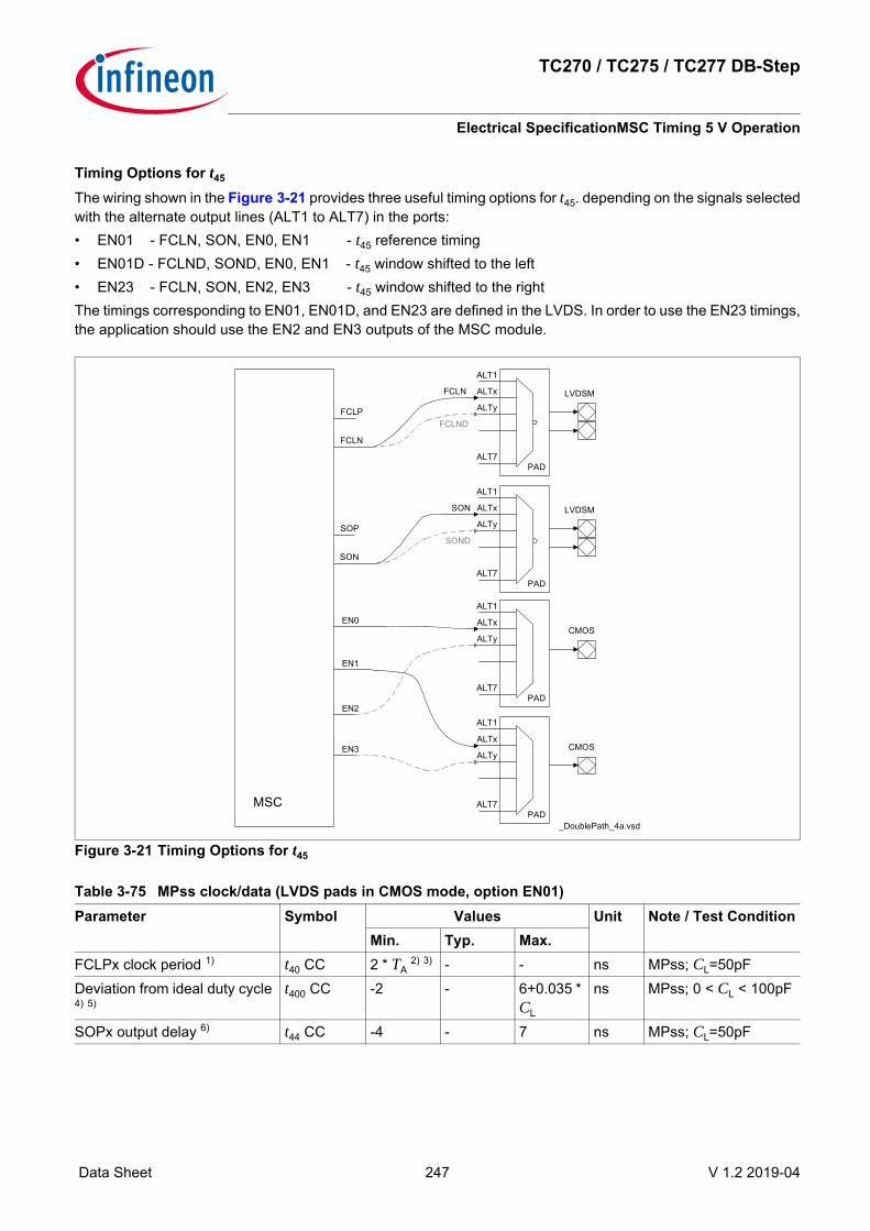
TC270 / TC275 / TC277 DB-Step
Electrical SpecificationMSC Timing 5 V Operation
Data Sheet 247 V 1.2 2019-04
Timing Options for t45
The wiring shown in the Figure 3-21 provides three useful timing options for t45. depending on the signals selectedwith the alternate output lines (ALT1 to ALT7) in the ports:• EN01 - FCLN, SON, EN0, EN1 - t45 reference timing• EN01D - FCLND, SOND, EN0, EN1 - t45 window shifted to the left• EN23 - FCLN, SON, EN2, EN3 - t45 window shifted to the rightThe timings corresponding to EN01, EN01D, and EN23 are defined in the LVDS. In order to use the EN23 timings,the application should use the EN2 and EN3 outputs of the MSC module.
Figure 3-21 Timing Options for t45
Table 3-75 MPss clock/data (LVDS pads in CMOS mode, option EN01)Parameter Symbol Values Unit Note / Test Condition
Min. Typ. Max.FCLPx clock period 1) t40 CC 2 * TA 2) 3) - - ns MPss; CL=50pFDeviation from ideal duty cycle 4) 5)
t400 CC -2 - 6+0.035 * CL
ns MPss; 0 < CL < 100pF
SOPx output delay 6) t44 CC -4 - 7 ns MPss; CL=50pF
MSC
PAD
EN0ALT1
ALTx
ALTy
ALT7
PAD
EN1
ALT1
ALTx
ALTy
ALT7
PAD
ALT1
ALTx
ALTy
ALT7
PAD
ALT1
ALTx
ALTy
ALT7
FCLP
FCLN
SOP
SON
LVDSM
LVDSM
EN2
EN3
FCLN
FCLND
SON
SOND
CMOS
CMOS
_DoublePath_4a.vsd

TC270 / TC275 / TC277 DB-Step
Electrical SpecificationMSC Timing 5 V Operation
Data Sheet 248 V 1.2 2019-04
ENx output delay 6) t45 CC -5 - 7 ns MP+ss/MPRss; CL=50pF
-2 - 15 ns MP+sm/MPRsm; CL=50pF
-4 - 10 ns MPss; CL=50pF0 - 30 ns MPsm; CL=50pF;
except pin P13.00 - 31 ns MPsm; CL=50pF; pin
P13.06 - 45 ns MPm/MP+m/MPRm;
CL=50pF-11 - 2 ns MP+ss/MPRss;
CL=0pF-4 - 7 ns MP+sm/MPRsm;
CL=0pF-10 - 2 ns MPss; CL=0pF-1 - 16 ns MPsm; CL=0pF-2 - 18 ns MP+m/MPm/MPRm;
CL=0pFSDI bit time t46 CC 8 * tMSC - - ns Upstream TimingSDI rise time 7) t48 SR - - 200 ns Upstream TimingSDI fall time 7) t49 SR - - 200 ns Upstream Timing1) FCLP signal rise/fall times are the rise/fall times of the LVDSM pads, and the high/low times are min 1 * TA.2) TA depends on the clock source selected for baud rate generation in the ABRA block of the MSC.3) FCLP signal high and low can be minimum 1 * TMSC.4) The PLL jitter is not included. It should be considered additionally, corresponding to the used baudrate. The duty cycle can
be adjusted if the ABRA block is used.5) Positive deviation lenghtens the high time and shortens the low time of a clock period. Negative deviation does the
opposite.6) From FCLP rising edge.7) When using slow and asymmetrical edges, like in case of open drain upstream connection, the application must take care
that the bit is long enough (the baud rate is low enough) so that under worst case conditions the three sampling points in the middle of the bit are not violated.
Table 3-76 MP+sm/MPRsm clock/dataParameter Symbol Values Unit Note / Test Condition
Min. Typ. Max.FCLPx clock period 1) t40 CC 2 * TA - - ns MP+sm/MPRsm;
CL=50pFDeviation from ideal duty cycle 2) 3)
t400 CC -2 - 3+0.01 * CL
ns MP+sm/MPRsm; 0 < CL < 200pF
SOPx output delay 4) t44 CC -5 - 7 ns MP+sm; CL=50pF
Table 3-75 MPss clock/data (LVDS pads in CMOS mode, option EN01) (cont’d)Parameter Symbol Values Unit Note / Test Condition
Min. Typ. Max.

TC270 / TC275 / TC277 DB-Step
Electrical SpecificationMSC Timing 5 V Operation
Data Sheet 249 V 1.2 2019-04
ENx output delay 4) t45 CC -13 - 2 5) ns MPss; CL=50pF-5 - 11 ns MP+sm/MPRsm;
CL=50pF1 - 24 ns MPsm; CL=50pF4 - 37 ns MP+m/MPm/MPRm;
CL=50pF-19 - -1 ns MPss; CL=0pF-13 - 2 ns MP+sm; CL=0pF-5 - 8 ns MPsm; CL=0pF-5 - 10 ns MPm/MP+m/MPRm;
CL=0pF1) FCLP signal rise/fall times are the rise/fall times of the LVDSM pads, and the high/low times are min 1 * TA.2) The PLL jitter is not included. It should be considered additionally, corresponding to the used baudrate. The duty cycle can
be adjusted if the ABRA block is used.3) Positive deviation lenghtens the high time and shortens the low time of a clock period. Negative deviation does the
opposite.4) From FCLP rising edge.5) If EN1 is configured to P13.0 the max limt is increased by 0.5ns to 2.5ns.
Table 3-77 MPm/MP+m/MPRm clock/dataParameter Symbol Values Unit Note / Test Condition
Min. Typ. Max.FCLPx clock period 1)
1) FCLP signal rise/fall times are the rise/fall times of the LVDSM pads, and the high/low times are min 1 * TA.
t40 CC 2 * TA - - ns MPm/MP+m/MPRm; CL=50pF
Deviation from ideal duty cycle 2) 3)
2) The PLL jitter is not included. It should be considered additionally, corresponding to the used baudrate. The duty cycle can be adjusted if the ABRA block is used.
3) Positive deviation lenghtens the high time and shortens the low time of a clock period. Negative deviation does the opposite.
t400 CC -8 - 15+0.04 * CL
ns MPm/MP+m; 0 < CL < 200pF
SOPx output delay 4)
4) From FCLP rising edge.
t44 CC -11 - 9 ns MPm/MP+m; CL=50pFENx output delay 4) t45 CC -15 - 11 ns MPm/MP+m/MPRm;
CL=50pF-33 - -4 ns MPm/MP+m/MPRm;
CL=0pF
Table 3-76 MP+sm/MPRsm clock/data (cont’d)Parameter Symbol Values Unit Note / Test Condition
Min. Typ. Max.

TC270 / TC275 / TC277 DB-Step
Electrical SpecificationMSC Timing 3.3 V Operation
Data Sheet 250 V 1.2 2019-04
Figure 3-22 MSC Interface Timing
Note: The SOP data signal is sampled with the falling edge of FCLP in the target device.
3.28 MSC Timing 3.3 V Operation
The following section defines the timings for 3.3V pad power supply.Note: Pad asymmetry is already included in the following timings.
Note: Load for LVDS pads are defined as differential loads in the following timings.
Mapping A, Combo Pads in LVDS Mode or CMOS ModeThe timing applies for the LVDS pads in LVDS operating mode:• The LVDSM output pads for clock and data signals set in LVDS mode• The CMOS MP pads for enable signals, with strong driver sharp edge (MPss) or strong driver medium edge
(MPsm).
Table 3-78 LVDS clock/data (LVDS pads in LVDS mode)Parameter Symbol Values Unit Note / Test Condition
Min. Typ. Max.FCLPx clock period 1) t40 CC 2 * TA 2) 3) - - ns LVDSM; CL=50pFDeviation from ideal duty cycle 4) 5)
t400 CC -2 - 2 ns LVDSM; 0 < CL < 50pF
SOPx output delay 6) t44 CC -5 - 5 ns LVDSM; CL=50pF; option EN01
-7 - 7 ns LVDSM; CL=50pF; option EN01D
MSC_Timing_A.vsd
t44 t44
t40
SOP
FCLP
SDI
t46
t48
0.1 VEXT/FLEX
0.9 VEXT/FLEX
t49
t46
t45 t45
EN
t400
0.5 VEXT/FLEX

TC270 / TC275 / TC277 DB-Step
Electrical SpecificationMSC Timing 3.3 V Operation
Data Sheet 251 V 1.2 2019-04
ENx output delay 6) t45 CC -7 - 10 ns MP+ss/MPRss; option EN01; CL=25pF
-5 - 13 ns MP+ss/MPRss; option EN01; CL=50pF
-5 - 26 ns MP+sm/MPRsm; option EN01D; CL=50pF
-4 - 16 ns MP+ss/MPRss; option EN23; CL=25pF
-4 - 17 ns MP+ss/MPRss; option EN23; CL=50pF
-5 - 19 ns MPss; option EN01; CL=50pF
-12 - 4 ns MP+ss/MPRss; option EN01; CL=0pF
-9 - 11 ns MP+sm/MPRsm; option EN01D; CL=0pF
-7 - 9 ns MP+ss/MPRss; option EN23; CL=0pF
-12 - 7 ns MPss; option EN01; CL=0pF
SDI bit time t46 CC 8 * tMSC - - ns Upstream TimingSDI rise time 7) t48 SR - - 200 ns Upstream TimingSDI fall time 7) t49 SR - - 200 ns Upstream Timing1) FCLP signal rise/fall times are the rise/fall times of the LVDSM pads, and the high/low times are min 1 * TA.2) TAmin = TMAX. When TMAX = 100 MHz,t40 = 20 ns3) The capacitive load on the LVDS pins is differential, the capacitive load on the CMOS pins is single ended. 4) The PLL jitter is not included. It should be considered additionally, corresponding to the used baudrate. The duty cycle can
be adjusted if the ABRA block is used.5) Positive deviation lenghtens the high time and shortens the low time of a clock period. Negative deviation does the
opposite.6) From FCLP rising edge.7) When using slow and asymmetrical edges, like in case of open drain upstream connection, the application must take care
that the bit is long enough (the baud rate is low enough) so that under worst case conditions the three sampling points in the middle of the bit are not violated.
Table 3-79 MPss clock/data (LVDS pads in CMOS mode, option EN01)Parameter Symbol Values Unit Note / Test Condition
Min. Typ. Max.FCLPx clock period 1) t40 CC 2 * TA 2) 3) - - ns MPss; CL=50pFDeviation from ideal duty cycle 4) 5)
t400 CC -5 - 7+0.07 * CL
ns MPss; 0 < CL < 100pF
Table 3-78 LVDS clock/data (LVDS pads in LVDS mode) (cont’d)Parameter Symbol Values Unit Note / Test Condition
Min. Typ. Max.

TC270 / TC275 / TC277 DB-Step
Electrical SpecificationMSC Timing 3.3 V Operation
Data Sheet 252 V 1.2 2019-04
Mapping B, CMOS MP PadsThis timing applies for the dedicated CMOS pads, pin Mapping B:• MP strong sharp (MPss) output pads for the clock and the data signals• MP strong sharp or strong medium (MPss or MPsm) output pads for enable signals
SOPx output delay 6) t44 CC -7 - 12 ns MPss; CL=50pFENx output delay 6) t45 CC -9 - 12 ns MP+ss/MPRss;
CL=50pF-4 - 26 ns MP+sm/MPRsm;
CL=50pF-7 - 17 ns MPss; CL=50pF0 - 54 ns MPsm; CL=50pF;
except pin P13.00 - 58 ns MPsm; CL=50pF; pin
P13.04 - 77 ns MPm/MP+m/MPRm;
CL=50pF-19 - 4 ns MP+ss/MPRss;
CL=0pF-7 - 12 ns MP+sm/MPRsm;
CL=0pF-17 - 4 ns MPss; CL=0pF-2 - 28 ns MPsm; CL=0pF-4 - 31 ns MP+m/MPm/MPRm;
CL=0pFSDI bit time t46 CC 8 * tMSC - - ns Upstream TimingSDI rise time 7) t48 SR - - 200 ns Upstream TimingSDI fall time 7) t49 SR - - 200 ns Upstream Timing1) FCLP signal rise/fall times are the rise/fall times of the LVDSM pads, and the high/low times are min 1 * TA.2) TAmin = TMAX. When TMAX = 100 MHz,t40 = 20 ns3) FCLP signal high and low can be minimum 1 * TMSC.4) The PLL jitter is not included. It should be considered additionally, corresponding to the used baudrate. The duty cycle can
be adjusted if the ABRA block is used.5) Positive deviation lenghtens the high time and shortens the low time of a clock period. Negative deviation does the
opposite.6) From FCLP rising edge.7) When using slow and asymmetrical edges, like in case of open drain upstream connection, the application must take care
that the bit is long enough (the baud rate is low enough) so that under worst case conditions the three sampling points in the middle of the bit are not violated.
Table 3-79 MPss clock/data (LVDS pads in CMOS mode, option EN01) (cont’d)Parameter Symbol Values Unit Note / Test Condition
Min. Typ. Max.

TC270 / TC275 / TC277 DB-Step
Electrical SpecificationMSC Timing 3.3 V Operation
Data Sheet 253 V 1.2 2019-04
Table 3-80 MP+sm/MPRsm clock/dataParameter Symbol Values Unit Note / Test Condition
Min. Typ. Max.FCLPx clock period 1)
1) FCLP signal rise/fall times are the rise/fall times of the LVDSM pads, and the high/low times are min 1 * TA.
t40 CC 2 * TA - - ns MP+sm/MPRsm; CL=50pF
Deviation from ideal duty cycle 2) 3)
2) The PLL jitter is not included. It should be considered additionally, corresponding to the used baudrate. The duty cycle can be adjusted if the ABRA block is used.
3) Positive deviation lenghtens the high time and shortens the low time of a clock period. Negative deviation does the opposite.
t400 CC -3 - 7 ns MP+sm/MPRsm; 0 < CL < 200pF
SOPx output delay 4)
4) From FCLP rising edge.
t44 CC -9 - 12 ns MP+sm; CL=50pFENx output delay 4) t45 CC -20 - 4 ns MPss; CL=50pF
-9 - 19 ns MP+sm/MPRsm; CL=50pF
0 - 44 ns MPsm; CL=50pF0 - 63 ns MP+m/MPm/MPRm;
CL=50pF-33 - 0 ns MPss; CL=0pF-23 - 4 ns MP+sm/MPRsm;
CL=0pF-9 - 14 ns MPsm; CL=0pF-9 - 17 ns MPm/MP+m/MPRm;
CL=0pF
Table 3-81 MPm/MP+m/MPRm clock/dataParameter Symbol Values Unit Note / Test Condition
Min. Typ. Max.FCLPx clock period 1)
1) FCLP signal rise/fall times are the rise/fall times of the LVDSM pads, and the high/low times are min 1 * TA.
t40 CC 2 * TA - - ns MPm/MP+m/MPRm; CL=50pF
Deviation from ideal duty cycle 2) 3)
2) The PLL jitter is not included. It should be considered additionally, corresponding to the used baudrate. The duty cycle can be adjusted if the ABRA block is used.
3) Positive deviation lenghtens the high time and shortens the low time of a clock period. Negative deviation does the opposite.
t400 CC -6-0.07 * CL
- 6+0.07 * CL
ns MPm/MP+m/MPRm; 0 < CL < 200pF
SOPx output delay 4) t44 CC -19 - 17 ns MPm/MP+m; CL=50pFENx output delay 4) t45 CC -19 - 20 ns MPm/MP+m/MPRm;
CL=50pF-57 - 0 ns MPm/MP+m/MPRm;
CL=0pF

TC270 / TC275 / TC277 DB-Step
Electrical SpecificationMSC Timing 3.3 V Operation
Data Sheet 254 V 1.2 2019-04
Figure 3-23 MSC Interface Timing
Note: The SOP data signal is sampled with the falling edge of FCLP in the target device.
4) From FCLP rising edge.
MSC_Timing_A.vsd
t44 t44
t40
SOP
FCLP
SDI
t46
t48
0.1 VEXT/FLEX
0.9 VEXT/FLEX
t49
t46
t45 t45
EN
t400
0.5 VEXT/FLEX
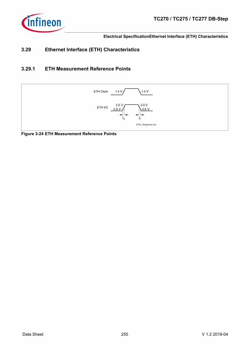
TC270 / TC275 / TC277 DB-Step
Electrical SpecificationEthernet Interface (ETH) Characteristics
Data Sheet 255 V 1.2 2019-04
3.29 Ethernet Interface (ETH) Characteristics
3.29.1 ETH Measurement Reference Points
Figure 3-24 ETH Measurement Reference Points
ETH_Testpoints.vsd
ETH Clock 1.4 V 1.4 V
2.0 V0.8 V
2.0 V0.8 V
tR tF
ETH I/O

TC270 / TC275 / TC277 DB-Step
Electrical SpecificationEthernet Interface (ETH) Characteristics
Data Sheet 256 V 1.2 2019-04
3.29.2 ETH Management Signal Parameters (ETH_MDC, ETH_MDIO)
Figure 3-25 ETH Management Signal Timing
Table 3-82 ETH Management Signal ParametersParameter Symbol Values Unit Note / Test Condition
Min. Typ. Max.ETH_MDC period t1 CC 400 - - ns CL=25pFETH_MDC high time t2 CC 160 - - ns CL=25pFETH_MDC low time t3 CC 160 - - ns CL=25pFETH_MDIO setup time (output) t4 CC 10 - - ns CL=25pFETH_MDIO hold time (output) t5 CC 10 - - ns CL=25pFETH_MDIO data valid (input) t6 SR 0 - 300 ns CL=25pF
ETH_Timing-Mgmt.vsd
ETH_MDC
ETH_MDIO(output )
t5
Valid Data
t4
Valid Data
t6
ETH_MDIO(input )
ETH_MDC
ETH_MDIO sourced by controller :
ETH_MDIO sourced by PHY:
ETH_MDC
t1
t3 t2

TC270 / TC275 / TC277 DB-Step
Electrical SpecificationEthernet Interface (ETH) Characteristics
Data Sheet 257 V 1.2 2019-04
3.29.3 ETH MII ParametersIn the following, the parameters of the MII (Media Independent Interface) are described.
Figure 3-26 ETH MII Signal Timing
Table 3-83 ETH MII Signal Timing ParametersParameter Symbol Values Unit Note / Test Condition
Min. Typ. Max.Clock period t7 SR 40 - - ns CL=25pF;
baudrate=100Mbps400 - - ns CL=25pF;
baudrate=10MbpsClock high time t8 SR 14 - 26 ns CL=25pF;
baudrate=100Mbps140 1)
1) Defined by 35% of clock period.
- 260 2)
2) Defined by 65% of clock period.
ns CL=25pF; baudrate=10Mbps
Clock low time t9 SR 14 - 26 ns CL=25pF; baudrate=100Mbps
140 1) - 260 2) ns CL=25pF; baudrate=10Mbps
Input setup time t10 SR 10 - - ns CL=25pFInput hold time t11 SR 10 - - ns CL=25pFOutput valid time t12 CC 0 - 25 ns CL=25pF
ETH_Timing-MII.vsd
ETH_MII_RX_CLK
ETH_MII_TXD[3:0]ETH_MII_TXEN
ETH_MII_RXD[3:0]ETH_MII_RX_DVETH_MII_RX_ER
ETH_MII_TX_CLK
t11
Valid Data
t10
Valid Data
t12
(sourced by controller )
(sourced by PHY)
t7
t9 t8ETH_MII_RX_CLKETH_MII_TX_CLK

TC270 / TC275 / TC277 DB-Step
Electrical SpecificationEthernet Interface (ETH) Characteristics
Data Sheet 258 V 1.2 2019-04
3.29.4 ETH RMII ParametersIn the following, the parameters of the RMII (Reduced Media Independent Interface) are described.
Figure 3-27 ETH RMII Signal Timing
Table 3-84 ETH RMII Signal Timing ParametersParameter Symbol Values Unit Note / Test Condition
Min. Typ. Max.ETH_RMII_REF_CL clock period
t13 CC 20 - - ns CL=25pF; 50ppm
ETH_RMII_REF_CL clock high time
t14 CC 7 1)
1) Defined by 35% of clock period.
- 13 2)
2) Defined by 65% of clock period.
ns CL=25pF
ETH_RMII_REF_CL clock low time
t15 CC 7 1) - 13 2) ns CL=25pF
ETHTXEN, ETHTXD[1:0], ETHRXD[1:0], ETHCRSDV, ETHRXER; setup time
t16 CC 4 - - ns CL=25pF
ETHTXEN, ETHTXD[1:0], ETHRXD[1:0], ETHCRSDV, ETHRXER; hold time
t17 CC 2 - - ns CL=25pF
ETH_Timing-RMII .vsd
ETH_RMII_REF_CL
t17
Valid Data
t16
t13
t15 t14
ETH_RMII_REF_CL
ETHTXEN, ETHTXD[1:0], ETHRXD[1:0],
ETHCRSDV, ETHRXER
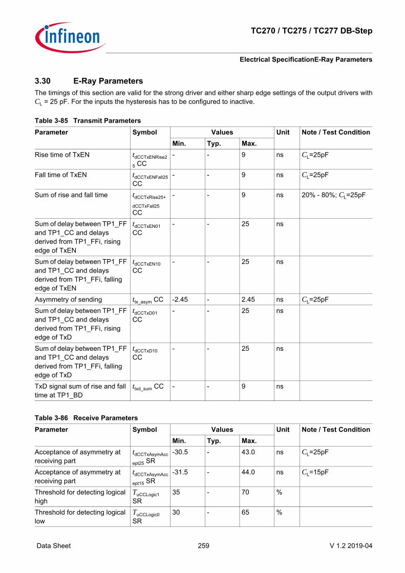
TC270 / TC275 / TC277 DB-Step
Electrical SpecificationE-Ray Parameters
Data Sheet 259 V 1.2 2019-04
3.30 E-Ray ParametersThe timings of this section are valid for the strong driver and either sharp edge settings of the output drivers withCL = 25 pF. For the inputs the hysteresis has to be configured to inactive.
Table 3-85 Transmit ParametersParameter Symbol Values Unit Note / Test Condition
Min. Typ. Max.Rise time of TxEN tdCCTxENRise2
5 CC- - 9 ns CL=25pF
Fall time of TxEN tdCCTxENFall25 CC
- - 9 ns CL=25pF
Sum of rise and fall time tdCCTxRise25+
dCCTxFall25 CC
- - 9 ns 20% - 80%; CL=25pF
Sum of delay between TP1_FF and TP1_CC and delays derived from TP1_FFi, rising edge of TxEN
tdCCTxEN01 CC
- - 25 ns
Sum of delay between TP1_FF and TP1_CC and delays derived from TP1_FFi, falling edge of TxEN
tdCCTxEN10 CC
- - 25 ns
Asymmetry of sending ttx_asym CC -2.45 - 2.45 ns CL=25pFSum of delay between TP1_FF and TP1_CC and delays derived from TP1_FFi, rising edge of TxD
tdCCTxD01 CC
- - 25 ns
Sum of delay between TP1_FF and TP1_CC and delays derived from TP1_FFi, falling edge of TxD
tdCCTxD10 CC
- - 25 ns
TxD signal sum of rise and fall time at TP1_BD
ttxd_sum CC - - 9 ns
Table 3-86 Receive ParametersParameter Symbol Values Unit Note / Test Condition
Min. Typ. Max.Acceptance of asymmetry at receiving part
tdCCTxAsymAcc
ept25 SR-30.5 - 43.0 ns CL=25pF
Acceptance of asymmetry at receiving part
tdCCTxAsymAcc
ept15 SR-31.5 - 44.0 ns CL=15pF
Threshold for detecting logical high
TuCCLogic1 SR
35 - 70 %
Threshold for detecting logical low
TuCCLogic0 SR
30 - 65 %

TC270 / TC275 / TC277 DB-Step
Electrical SpecificationE-Ray Parameters
Data Sheet 260 V 1.2 2019-04
Sum of delay between TP4_CC and TP4_FF and delays derived from TP4_FFi, rising edge of RxD
tdCCRxD01 CC
- - 10 ns
Sum of delay between TP1_CC and TP1_CC and delays derived from TP4_FFi, falling edge of RxD
tdCCRxD10 CC
- - 10 ns
Table 3-86 Receive Parameters (cont’d)Parameter Symbol Values Unit Note / Test Condition
Min. Typ. Max.
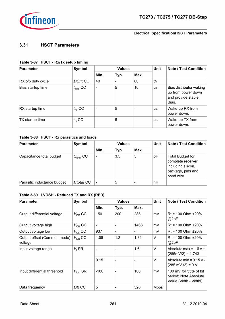
TC270 / TC275 / TC277 DB-Step
Electrical SpecificationHSCT Parameters
Data Sheet 261 V 1.2 2019-04
3.31 HSCT Parameters
Table 3-87 HSCT - Rx/Tx setup timingParameter Symbol Values Unit Note / Test Condition
Min. Typ. Max.RX o/p duty cycle DCrx CC 40 - 60 %Bias startup time tbias CC - 5 10 µs Bias distributor waking
up from power down and provide stable Bias.
RX startup time trxi CC - 5 - µs Wake-up RX from power down.
TX startup time ttx CC - 5 - µs Wake-up TX from power down.
Table 3-88 HSCT - Rx parasitics and loadsParameter Symbol Values Unit Note / Test Condition
Min. Typ. Max.Capacitance total budget Ctotal CC - 3.5 5 pF Total Budget for
complete receiver including silicon, package, pins and bond wire
Parasitic inductance budget Htotal CC - 5 - nH
Table 3-89 LVDSH - Reduced TX and RX (RED)Parameter Symbol Values Unit Note / Test Condition
Min. Typ. Max.Output differential voltage VOD CC 150 200 285 mV Rt = 100 Ohm ±20%
@2pFOutput voltage high VOH CC - - 1463 mV Rt = 100 Ohm ±20%Output voltage low VOL CC 937 - - mV Rt = 100 Ohm ±20%Output offset (Common mode) voltage
VOS CC 1.08 1.2 1.32 V Rt = 100 Ohm ±20% @2pF
Input voltage range VI SR - - 1.6 V Absolute max = 1.6 V + (285mV/2) = 1.743
0.15 - - V Absolute min = 0.15 V - (285 mV /2) = 0 V
Input differential threshold Vidth SR -100 - 100 mV 100 mV for 55% of bit period; Note Absolute Value (Vidth - Vidthl)
Data frequency DR CC 5 - 320 Mbps
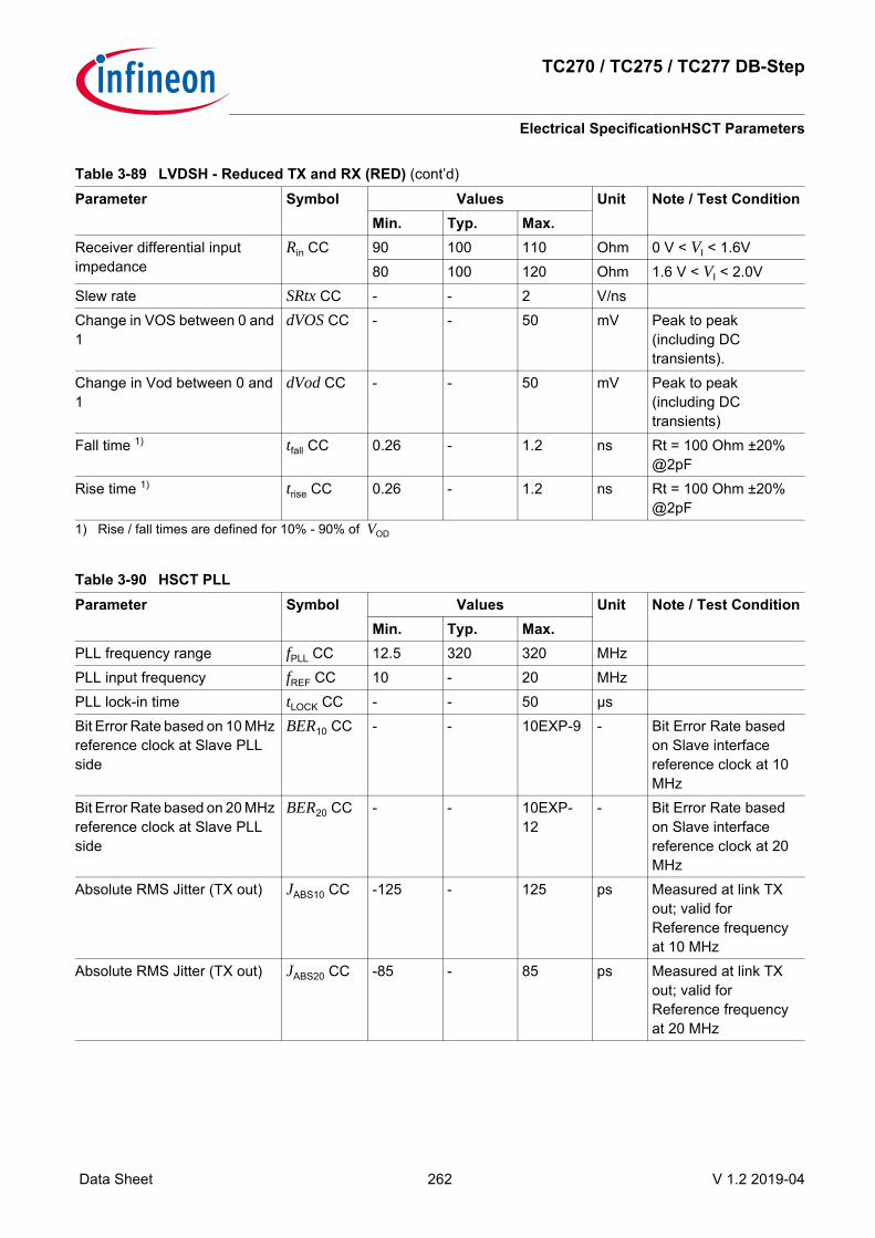
TC270 / TC275 / TC277 DB-Step
Electrical SpecificationHSCT Parameters
Data Sheet 262 V 1.2 2019-04
Receiver differential input impedance
Rin CC 90 100 110 Ohm 0 V < VI < 1.6V80 100 120 Ohm 1.6 V < VI < 2.0V
Slew rate SRtx CC - - 2 V/nsChange in VOS between 0 and 1
dVOS CC - - 50 mV Peak to peak (including DC transients).
Change in Vod between 0 and 1
dVod CC - - 50 mV Peak to peak (including DC transients)
Fall time 1) tfall CC 0.26 - 1.2 ns Rt = 100 Ohm ±20% @2pF
Rise time 1) trise CC 0.26 - 1.2 ns Rt = 100 Ohm ±20% @2pF
1) Rise / fall times are defined for 10% - 90% of VOD
Table 3-90 HSCT PLLParameter Symbol Values Unit Note / Test Condition
Min. Typ. Max.PLL frequency range fPLL CC 12.5 320 320 MHzPLL input frequency fREF CC 10 - 20 MHzPLL lock-in time tLOCK CC - - 50 µsBit Error Rate based on 10 MHz reference clock at Slave PLL side
BER10 CC - - 10EXP-9 - Bit Error Rate based on Slave interface reference clock at 10 MHz
Bit Error Rate based on 20 MHz reference clock at Slave PLL side
BER20 CC - - 10EXP-12
- Bit Error Rate based on Slave interface reference clock at 20 MHz
Absolute RMS Jitter (TX out) JABS10 CC -125 - 125 ps Measured at link TX out; valid for Reference frequency at 10 MHz
Absolute RMS Jitter (TX out) JABS20 CC -85 - 85 ps Measured at link TX out; valid for Reference frequency at 20 MHz
Table 3-89 LVDSH - Reduced TX and RX (RED) (cont’d)Parameter Symbol Values Unit Note / Test Condition
Min. Typ. Max.

TC270 / TC275 / TC277 DB-Step
Electrical SpecificationHSCT Parameters
Data Sheet 263 V 1.2 2019-04
Accumulated RMS Jitter (RX side)
JACC10 CC - - 145 ps Measured at link RX input, based on 5000 measures, each 300 clock cycles; valid for Reference frequency at 10 MHz
Accumulated RMS Jitter (link RX side)
JACC20 CC - - 115 ps Measured at link RX input, based on 5000 measures, each 300 clock cycles; valid for Reference frequency at 20 MHz
Total Jitter peak to peak TJpp CC - - 2083 ps Total Jitter as sum of deterministic jitter and random jitter
Table 3-91 HSCT SysclkParameter Symbol Values Unit Note / Test Condition
Min. Typ. Max.Frequency fSYSCLK CC 10 - 20 MHzFrequency error dfERR CC -1 - 1 %Duty Cycle DCsys CC 45 - 55 %Load impedance RLOAD CC 10 - - kOhmLoad capacitance CLOAD CC - - 10 pFIntegrated phase noise IPN CC - - -58 dB single sideband phase
noise in 10 kHz to 10 Mhz at 20 MHz SysClk
Table 3-90 HSCT PLL (cont’d)Parameter Symbol Values Unit Note / Test Condition
Min. Typ. Max.

TC270 / TC275 / TC277 DB-Step
Electrical SpecificationInter-IC (I2C) Interface Timing
Data Sheet 264 V 1.2 2019-04
3.32 Inter-IC (I2C) Interface TimingThis section defines the timings for I2C in the TC270 / TC275 / TC277.All I2C timing parameter are SR for Master Mode and CC for Slave Mode.
Table 3-92 I2C Standard Mode TimingParameter Symbol Values Unit Note / Test Condition
Min. Typ. Max.Fall time of both SDA and SCL t1 - - 300 ns Measured with a pull-
up resistor of 4.7 kohms at each of the SCL and SDA line
Capacitive load for each bus line
Cb SR - - 400 pF
Bus free time between a STOP and ATART condition
t10 4.7 - - µs Measured with a pull-up resistor of 4.7 kohms at each of the SCL and SDA line
Rise time of both SDA and SCL t2 - - 1000 ns Measured with a pull-up resistor of 4.7 kohms at each of the SCL and SDA line
Data hold time t3 0 - - µs Measured with a pull-up resistor of 4.7 kohms at each of the SCL and SDA line
Data set-up time t4 250 - - ns Measured with a pull-up resistor of 4.7 kohms at each of the SCL and SDA line
Low period of SCL clock t5 4.7 - - µs Measured with a pull-up resistor of 4.7 kohms at each of the SCL and SDA line
High period of SCL clock t6 4 - - µs Measured with a pull-up resistor of 4.7 kohms at each of the SCL and SDA line
Hold time for the (repeated) START condition
t7 4 - - µs Measured with a pull-up resistor of 4.7 kohms at each of the SCL and SDA line
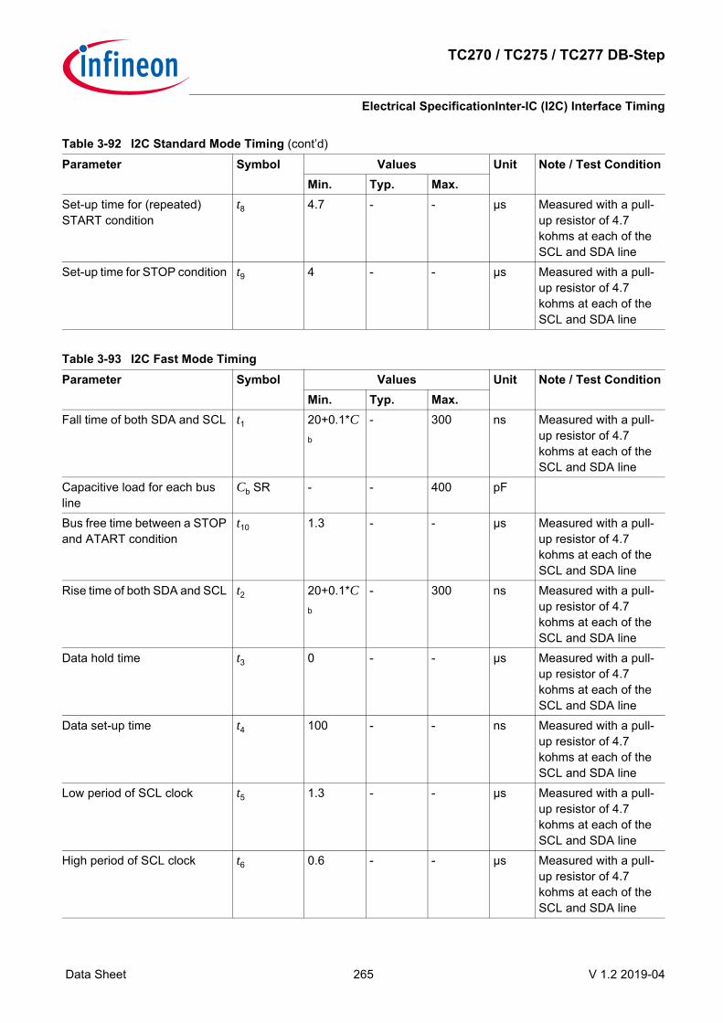
TC270 / TC275 / TC277 DB-Step
Electrical SpecificationInter-IC (I2C) Interface Timing
Data Sheet 265 V 1.2 2019-04
Set-up time for (repeated) START condition
t8 4.7 - - µs Measured with a pull-up resistor of 4.7 kohms at each of the SCL and SDA line
Set-up time for STOP condition t9 4 - - µs Measured with a pull-up resistor of 4.7 kohms at each of the SCL and SDA line
Table 3-93 I2C Fast Mode TimingParameter Symbol Values Unit Note / Test Condition
Min. Typ. Max.Fall time of both SDA and SCL t1 20+0.1*C
b - 300 ns Measured with a pull-
up resistor of 4.7 kohms at each of the SCL and SDA line
Capacitive load for each bus line
Cb SR - - 400 pF
Bus free time between a STOP and ATART condition
t10 1.3 - - µs Measured with a pull-up resistor of 4.7 kohms at each of the SCL and SDA line
Rise time of both SDA and SCL t2 20+0.1*Cb
- 300 ns Measured with a pull-up resistor of 4.7 kohms at each of the SCL and SDA line
Data hold time t3 0 - - µs Measured with a pull-up resistor of 4.7 kohms at each of the SCL and SDA line
Data set-up time t4 100 - - ns Measured with a pull-up resistor of 4.7 kohms at each of the SCL and SDA line
Low period of SCL clock t5 1.3 - - µs Measured with a pull-up resistor of 4.7 kohms at each of the SCL and SDA line
High period of SCL clock t6 0.6 - - µs Measured with a pull-up resistor of 4.7 kohms at each of the SCL and SDA line
Table 3-92 I2C Standard Mode Timing (cont’d)Parameter Symbol Values Unit Note / Test Condition
Min. Typ. Max.

TC270 / TC275 / TC277 DB-Step
Electrical SpecificationInter-IC (I2C) Interface Timing
Data Sheet 266 V 1.2 2019-04
Hold time for the (repeated) START condition
t7 0.6 - - µs Measured with a pull-up resistor of 4.7 kohms at each of the SCL and SDA line
Set-up time for (repeated) START condition
t8 0.6 - - µs Measured with a pull-up resistor of 4.7 kohms at each of the SCL and SDA line
Set-up time for STOP condition t9 0.6 - - µs Measured with a pull-up resistor of 4.7 kohms at each of the SCL and SDA line
Table 3-93 I2C Fast Mode Timing (cont’d)Parameter Symbol Values Unit Note / Test Condition
Min. Typ. Max.

TC270 / TC275 / TC277 DB-Step
Electrical SpecificationFlash Target Parameters
Data Sheet 267 V 1.2 2019-04
3.33 Flash Target Parameters Program Flash program and erase operation is only allowed up the TJ = 150°C.
Table 3-94 FLASHParameter Symbol Values Unit Note / Test Condition
Min. Typ. Max.Program Flash Erase Time per logical sector
tERP CC - - 1 s cycle count < 1000- 0.207 +
0.003 * (S [KByte]) / (fFSI [MHz])1)
- s cycle count < 1000, for sector of size S
Program Flash Erase Time per Multi-Sector Command
tMERP CC - - 1 s For consecutive logical sectors in a physical sector, cycle count < 1000
- 0.207 + 0.003 * (S [KByte]) / (fFSI [MHz])1)
- s For consecutive logical sector range of size S in a physical sector, cycle count < 1000
Program Flash program time per page in 5 V mode
tPRP5 CC - - 50 + 3000/(fFSI [MHz])
µs 32 Byte
Program Flash program time per page in 3.3 V mode
tPRP3 CC - - 81 + 3400/(fFSI [MHz])
µs 32 Byte
Program Flash program time per burst in 5 V mode
tPRPB5 CC - - 125 + 9500/(fFSI [MHz])
µs 256 Byte
Program Flash program time per burst in 3.3 V mode
tPRPB3 CC - - 410 + 12000/(fF
SI [MHz])
µs 256 Byte
Program Flash program time for 1 MByte with burst programming in 3 V mode excluding communication
tPRPB3_1MB CC
- - 2.2 s Derived value for documentation purpose, valid for fFSI = 100MHz
Program Flash program time for 1 MByte with burst programming in 5 V mode excluding communication
tPRPB5_1MB CC
- - 0.9 s Derived value for documentation purpose, valid for fFSI = 100MHz
Program Flash program time for complete PFlash with burst programming in 5 V mode excluding communication
tPRPB5_PF CC
- - 3.6 s Derived value for documentation purpose, valid for fFSI = 100MHz

TC270 / TC275 / TC277 DB-Step
Electrical SpecificationFlash Target Parameters
Data Sheet 268 V 1.2 2019-04
Write Page Once adder tADD CC - - 15 + 500/(fFSI [MHz])
µs Adder to Program Time when using Write Page Once
Program Flash suspend to read latency
tSPNDP CC - - 12000/(fF
SI [MHz]) µs For Write Burst, Verify
Erased and for multi-(logical) sector erase commands
Data Flash Erase Time per Sector 2)
tERD CC - 0.12 + 0.08/(fFSI [MHz])1)
- s cycle count < 1000
- 0.57 + 0.15/(fFSI [MHz])1)
0.928 + 0.15/(fFSI [MHz])
s cycle count < 125000
Data Flash Erase Time per Multi-Sector Command 2)
tMERD CC - 0.12 + 0.01 * (S [KByte]) / (fFSI [MHz])1)
- s For consecutive logical sector range of size S, cycle count < 1000
- 0.57 + 0.019 * (S [KByte]) / (fFSI [MHz])1)
0.928 + 0.019 * (S [KByte]) / (fFSI [MHz])
s For consecutive logical sector range of size S, cycle count < 125000
Data Flash erase disturb limit NDFD CC - - 50 cyclesProgram time data flash per page 3)
tPRD CC - - 50 + 2500/(fFSI [MHz]) 3)
µs 8 Byte
Complete Device Flash Erase Time PFlash and DFlash 4)
tER_Dev CC - - 9 s Derived value for documentation purpose (excl. UCBs and HSMs), valid for fFSI = 100MHz
Data Flash program time per burst 3)
tPRDB CC - - 96 + 4400/(fFSI [MHz]) 3)
µs 32 Bytes
Data Flash suspend to read latency
tSPNDD CC - - 12000/(fF
SI [MHz]) µs
Wait time after margin change tFL_MarginDel CC
- - 10 µs
Program Flash Retention Time, Sector
tRET CC 20 - - years Max. 1000 erase/program cycles
Data Flash Endurance per EEPROMx sector 5)
NE_EEP10 CC
125000 - - cycles Max. data retention time 10 years
Table 3-94 FLASH (cont’d)Parameter Symbol Values Unit Note / Test Condition
Min. Typ. Max.

TC270 / TC275 / TC277 DB-Step
Electrical SpecificationFlash Target Parameters
Data Sheet 269 V 1.2 2019-04
Data Flash Endurance per HSMx sector 5)
NE_HSM CC 125000 - - cycles Max. data retention time 10 years
UCB Retention Time tRTU CC 20 - - years Max. 100 erase/program cycles per UCB, max 400 erase/program cycles in total
Data Flash access delay tDF CC - - 100 ns see PMU_FCON.WSDFLASH
Data Flash ECC Delay tDFECC CC - - 20 ns see PMU_FCON.WSECDF
Program Flash access delay tPF CC - - 30 ns see PMU_FCON.WSPFLASH
Program Flash ECC delay tPFECC CC - - 10 ns see PMU_FCON.WSECPF
Number of erase operations on DF0 over lifetime
NERD0 CC - - 750000 cycles
Number of erase operations on DF1 over lifetime
NERD1 CC - - 500000 cycles
Junction temperature limit for PFlash program/erase operations
TJPFlash SR - - 150 °C
1) All typical values were characterised, but are not tested. Typical values are safe median values at room temperature2) Under out-of-spec conditions (e.g. over-cycling) or in case of activation of WL oriented defects, the duration of erase
processes may be increased by up to 50%.3) Time is not dependent on program mode (5V or 3.3V).4) Using 512 KByte erase commands.5) Only valid when a robust EEPROM emulation algorithm is used. For more details see the Users Manual.
Table 3-94 FLASH (cont’d)Parameter Symbol Values Unit Note / Test Condition
Min. Typ. Max.

TC270 / TC275 / TC277 DB-Step
Electrical SpecificationPackage Outline
Data Sheet 270 V 1.2 2019-04
3.34 Package Outline
Figure 3-28 Package Outlines PG-LQFP-176-22
Figure 3-29 Package Outlines LF-BGA-292-6 / LF-BGA-292-10
You can find all of our packages, sorts of packing and others in our Infineon Internet Page “Products”:http://www.infineon.com/products.
Table 3-95 Exposed Pad DimensionsAx (nominal EPad size) 7.9 mm ± 50 µmAy (nominal EPad size) 7.9 mm ± 50 µmEx (solder able EPad size) 8.7 mm ± 50 µmEy (solder able EPad size) 8.7 mm ± 50 µm
CODE
STANDOFF
ABCDEFGHJK12345678910
INDEX
MARKING(LASERED )INDEX MARKING
0.1 C
1112
LM
1314
P N
SEAT
ING
PLAN
E
0.8
18
15
1716
2019
RTUVWY
COPLANARITY
292x
0.15
0.08 M C0.15 M C A B
292x
C
AB
17±0
.1
17 ±0.1
0.33 MIN
1.7 MAX
0.5 ±0.05
19 x 0.8 = 15.2
0.8
19 x
0.8
= 15
.2

TC270 / TC275 / TC277 DB-Step
Electrical SpecificationPackage Outline
Data Sheet 271 V 1.2 2019-04
3.34.1 Package Parameters
3.34.2 TC270 Carrier Tape
Figure 3-30 Carrier Tape Dimenions
Table 3-96 Thermal Characteristics of the PackageDevice Package RQJCT1)
1) The top and bottom thermal resistances between the case and the ambient (RTCAT, RTCAB) are to be combined with the thermal resistances between the junction and the case given above (RTJCT, RTJCB), in order to calculate the total thermal resistance between the junction and the ambient (RTJA). The thermal resistances between the case and the ambient (RTCAT, RTCAB) depend on the external system (PCB, case) characteristics, and are under user responsibility.The junction temperature can be calculated using the following equation: TJ = TA + RTJA * PD, where the RTJA is the total thermal resistance between the junction and the ambient. This total junction ambient resistance RTJA can be obtained from the upper four partial thermal resistances.Thermal resistances as measured by the ’cold plate method’ (MIL SPEC-883 Method 1012.1).
RQJCB1) RQJA Unit NoteTC275 PG-LQFP-176-22 9,6 1,25 14,72)
2) Value is defined in accordance with JEDEC JESD51-3, JESD51-5, and JESD51-7.
K/W with soldered exposed pad
TC277 LF-BGA-292-6 / LF-BGA-292-10
5,1 7,2 15,83)
3) Value is defined in accordance with JEDEC JESD51-1.
K/W

TC270 / TC275 / TC277 DB-Step
Electrical SpecificationPackage Outline
Data Sheet 272 V 1.2 2019-04
Table 3-97 TC270 Chip DimenionsDevice A B TTC270 7,590 mm 6,930 mm 0,3 mm

TC270 / TC275 / TC277 DB-Step
Electrical SpecificationQuality Declarations
Data Sheet 273 V 1.2 2019-04
3.35 Quality Declarations
Table 3-98 Quality ParametersParameter Symbol Values Unit Note / Test Condition
Min. Typ. Max.Operation Lifetime tOP - - 24500 hourESD susceptibility according to Human Body Model (HBM)
VHBM - - 2000 V Conforming to JESD22-A114-B
ESD susceptibility of the LVDS pins
VHBM1 - - 500 V
ESD susceptibility according to Charged Device Model (CDM)
VCDM - - 500 V for all other balls/pins; conforming to JESD22-C101-C
- - 750 V for corner balls/pins; conforming to JESD22-C101-C
Moisture Sensitivity Level MSL - - 3 Conforming to Jedec J-STD--020C for 240C

TC270 / TC275 / TC277 DB-Step
HistoryChanges from version version 0.6 to 0.7
Data Sheet 274 V 1.2 2019-04
4 HistoryVersion 0.6 is the first version of this document.
4.1 Changes from version version 0.6 to 0.7
• Changes in table 'Overload Parameters' of Overload– Add max 1.7*10-3 to KOVDN – Add max 2*10-2 to KOVDN – Add max 1*10-2 to KOVDN – Add max 1*10-4 to KOVDP – Add max 1*10-2 to KOVAN – Change note of KOVAN from '-5mA < IIN < -1mA' to 'Analog Inputs overlaid with class LP pads or pull down
diagnostics; -5mA < IIN < -1mA' – Change max value of KOVAN from 3*10-3 to 1*10-2 – Change min value of IINANA from -1 mA to -3 mA – Change note of KOVAN from 'else' to 'else; -5mA < IIN < 0mA' – Change note of KOVAP from 'else' to '5mA < IIN < 0mA' – Change max value of KOVAN from 1*10-3 to 6*10-4 – Change note of KOVAN from 'Analog Inputs overlaid with class LP pads or pull down diagnostics' to 'Analog
Inputs overlaid with class LP pads or pull down diagnostics; -1mA < IIN < 0mA' – Change note of KOVDP from 'Overload injected on LVDS pad and affecting neighbor LVDS pad' to 'Overload
injected on LVDS pad and affecting neighbor LVDS pads' – Change note of KOVDP from 'Overload injected on GPIO non LVDS pad and affecting neighbor GPIO non
LVDS pad' to 'Overload injected on GPIO non LVDS pad and affecting neighbor GPIO non LVDS pads' – Change max value of KOVDN from 0.9 to 0.93 – Change note of KOVDN from 'Overload injected on GPIO non LVDS pad and affecting neighbor GPIO non
LVDS pad' to 'Overload injected on GPIO non LVDS pad and affecting neighbor LP and A2 pads; -2mA < IIN < 0mA'
– Change max value of KOVDN from 1.5*10-3 to 6*10-4 – Change note of KOVDN from 'Overload injected on LVDS pad and affecting neighbor LVDS pad' to 'Overload
injected on LVDS pad and affecting neighbor LVDS pads' • VADC
– Add min 0 pC to QCONV – Add min 8 pC to QCONV – Add max 10 pC to QCONV – Add max 2 µA to IOZ2 – Change min value of IOZ3 from -2.5 µA to -3.3 µA – Change note of IOZ3 from '-1 µA' to '-2 µA'– Change max value of IOZ2 from 2 µA to 3 µA– Add min -2.8 µA to IOZ3 – Add max 2.5 µA to IOZ3 – Add max 20 pC to QCONV – Add min -2 µA to IOZ2

TC270 / TC275 / TC277 DB-Step
HistoryChanges from version version 0.6 to 0.7
Data Sheet 275 V 1.2 2019-04
– Add min VSSM V to VAGND – Add max 7 µA to IOZ2 – Add min -13 µA to IOZ3 – Add min -4 µA to IOZ2 – Add max 4 µA to IOZ2 – Add min -7 µA to IOZ3 – Add max 7 µA to IOZ3 – Add max 13 µA to IOZ3 – Add typ 0.5 LSB to ENRMS – Add min -7 µA to IOZ2 – Change note of QCONV from 'VAIN = 5V, charge consumed from reference pin, precharging disabled' to 'VAIN
= 5 V, charge consumed from reference pin, precharging disabled' – Change typ value of QCONV from 80 pC to 14 pC – Change predicate of tBWG from typ to max – Change max value of tBWG from 50 cycles to 120 cycles – Change predicate of tBWR from typ to max – Change max value of tBWR from 50 cycles to 60 cycles – Change note of IOZ1 from 'Analog Inputs overlaid with GPIO functions or pull down diagnosis or DSADC
inputs' to 'Analog Inputs overlaid with class LP pads or pull down diagnostics' – Change note of QCONV from 'VAIN = 5V, charge consumed from reference pin, precharging enabled' to 'VAIN
= 5 V, charge consumed from reference pin, precharging enabled' – Change typ value of QCONV from 20 pC to 3 pC – Change note of ENRMS from 'target' to '' – Change max value of ENRMS from 0.5 LSB to 0.75 LSB – Change note of RAIN from 'valid for analoge inputs mapped to GPIOs' to 'valid for analog inputs mapped to
GPIOs' • VADC_33V
– Add min 0 pC to QCONV – Add min 4 pC to QCONV – Add max 15 pC to QCONV – Add max 8 pC to QCONV – Add min -2 µA to IOZ2 – Add max 2.5 µA to IOZ2 – Add min -2.2 µA to IOZ3 – Add max 2 µA to IOZ3 – Add max 12 µA to IOZ3 – Add min -6 LSB to EAGAIN – Add min -12 LSB to TUE – Add max 12 LSB to TUE – Add min -12 LSB to EAINL – Add max 12 LSB to EAINL – Add min -6 LSB to EAOFF

TC270 / TC275 / TC277 DB-Step
HistoryChanges from version version 0.6 to 0.7
Data Sheet 276 V 1.2 2019-04
– Add max 6 LSB to EAOFF – Add max 6 LSB to EAGAIN – Add min -3.5 µA to IOZ2 – Add min -6 µA to IOZ2 – Add max 3.5 µA to IOZ2 – Add max 6 µA to IOZ2 – Add min -6.5 µA to IOZ3 – Add min -12 µA to IOZ3 – Add max 6.5 µA to IOZ3 – Add max 150 °C to TJ – Add min VSSM V to VAGND – Add min 150 °C to TJ – Add max 10 % to dVCSD – Add max 28 kOhm to RCSD – Change note of TUE from '12-bit resolution' to '12-bit Resolution; TJ ≤ 150 °C' – Change note of EADNL from '' to '12-bit resolution' – Change note of EAINL from '' to '12-bit Resolution; TJ ≤ 150 °C' – Change note of EAOFF from '' to '12-bit Resolution; TJ ≤ 150 °C' – Change note of EAGAIN from '' to '12-bit Resolution; TJ ≤ 150 °C' – Change note of IOZ1 from 'Analog Inputs overlaid with GPIO functions or pull down diagnosis or DSADC
inputs' to 'Analog Inputs overlaid with class LP pads or pull down diagnostics' – Change note of QCONV from 'VAIN = 3.3V, charge consumed from reference pin, precharging disabled' to
'VAIN = 3.3 V, charge consumed from reference pin, precharging disabled' – Change typ value of QCONV from 60 pC to 7 pC – Change note of QCONV from 'VAIN = 3.3V, charge consumed from reference pin, precharging enabled' to
'VAIN = 3.3 V, charge consumed from reference pin, precharging enabled' – Change typ value of QCONV from 15 pC to 3 pC – Change max value of tBWG from 50 cycles to 120 cycles – Change predicate of tBWG from typ to max – Change max value of tBWR from 50 cycles to 60 cycles – Change predicate of tBWR from typ to max – Change description of IOZ2 from 'Positive reference pin leakage' to 'Positive reference VAREFx pin leakage' – Change description of IOZ3 from 'Negative reference pin leakage' to 'Negative reference VAGNDx pin leakage' – Add footnote 'This parameter is valid for soldered devices and requires careful analog board design.' to
ENRMS – Change max value of RAIN from 1.5 kOhm to 1.6 kOhm
• EVR/LDO/1.3V– Add max 6.3 µF to COUT – Add min 3 µF to COUT – Change note of dVout/dIout from 'dI=-150mA; Tsettle=20µs; pass device=off chip' to 'dI=-150mA;
Tsettle=20µs; pass device=off chip' • EVR/Back-up Clock
– Add footnote 'All VEXT pins shall be connected together externally on the PCB.' to VEXT

TC270 / TC275 / TC277 DB-Step
HistoryChanges from version version 0.6 to 0.7
Data Sheet 277 V 1.2 2019-04
• Changes in table 'EVR13 SMPS External components' of EVR/DCDC– Change name of COUTDC from CDC to COUTDC
• Changes in table 'EVR13 SMPS' of EVR/DCDC– Change note of dVout/dIout from 'dI < 200mA ; fDCDC=1MHz; tr=0.1us; tf=0.1us; VDDDC=1.3V' to 'dI <
200mA ; fDCDC=1MHz; tr=0.1µs; tf=0.1µs; VDDDC=1.3V' – Change note of dVout/dIout from 'dI < 700mA ; fDCDC=1MHz; tr=0.1us; tf=0.1us; VDDDC=1.3V' to 'dI <
700mA ; fDCDC=1MHz; tr=0.1µs; tf=0.1µs; VDDDC=1.3V' – Change note of dVout/dIout from 'dI < 400mA ; fDCDC=1MHz; tr=0.1us; tf=0.1us; VDDDC=1.3V' to 'dI <
400mA ; fDCDC=1MHz; tr=0.1µs; tf=0.1µs; VDDDC=1.3V' – Add footnote 'Incase of SMPS mode, It shall be ensured that the VDD Output pin shall be connected on
PCB level to all other VDD Input pins.' to VDDDC – Add footnote 'Capacitor min-max range represent typical ±35% tolerance including DC bias effect. The
trace resistance from the capacitor to the supply or ground rail should be limited to 25 mOhm.' to COUTDC – Add footnote 'Incase of TC29x running with fSRI = 300 MHz, it shall be ensured that the VDD operating
range is limited to 1.235V upto 1.430V. The DCDC may be configured in this case with a nominal voltage of 1.33V±7.5%. The static accuracy and regulation parameter ranges remain also valid for this case.' to VDD_DC
• FLASH– Add max 2.2 s to tPRPB3_1MB – Change note of tERD from '' to 'cycle count < 125000' – Change max value of tERD from 1 s to 0.928 + 0.15/(fFSI [MHz]) s – Change max value of tPRD from 75 µs to 50 + 2500/(fFSI [MHz]) µs – Change note of tMERP from 'For consecutive logical sectors in a physical sector' to 'For consecutive logical
sectors in a physical sector, cycle count < 1000' – Change max value of tPRP5 from 80 µs to 50 + 3000/(fFSI [MHz]) µs – Change max value of tPRPB5 from 220 µs to 125 + 9500/(fFSI [MHz]) µs – Change max value of tPRPB3 from 530 µs to 410 + 12000/(fFSI [MHz]) µs – Change note of tPRPB5_1MB from 'Derived value for documentation purpose' to 'Derived value for
documentation purpose, valid for fFSI = 100MHz' – Change note of tPRPB5_PF from 'Derived value for documentation purpose' to 'Derived value for
documentation purpose, valid for fFSI = 100MHz' – Change max value of tADD from 20 µs to 15 + 500/(fFSI [MHz]) µs – Change max value of tSPNDP from 120 µs to 12000/(fFSI [MHz]) µs – Change note of tMERD from 'For consecutive logical sectors' to 'For consecutive logical sector range of size
S, cycle count < 125000' – Change max value of tMERD from 1 s to 0.928 + 0.019 * (S [KByte]) / (fFSI [MHz]) s – Change note of tER_Dev from 'Derived value for documentation purpose (excl. UCBs and HSMs)' to 'Derived
value for documentation purpose (excl. UCBs and HSMs); valid for fFSI = 100MHz' – Change max value of tPRDB from 140 µs to 96 + 4400/(fFSI [MHz]) µs – Change max value of tSPNDD from 120 µs to 12000/(fFSI [MHz]) µs – Change max value of tPRP3 from 115 µs to 81 + 3400/(fFSI [MHz]) µs – Add typ 0.12 + 0.08/(fFSI [MHz]) s to tERD – Add typ 0.207 + 0.003 * (S [KByte]) / (fFSI [MHz]) s to tMERP – Add typ 0.12 + 0.01 * (S [KByte]) / (fFSI [MHz]) s to tMERD
TC270 / TC275 / TC277 DB-Step
HistoryChanges from version version 0.6 to 0.7
Data Sheet 278 V 1.2 2019-04
– Add typ 0.207 + 0.003 * (S [KByte]) / (fFSI [MHz]) s to tERP – Add typ 0.57 + 0.15/(fFSI [MHz]) s to tERD – Add typ 0.57 + 0.019 * (S [KByte]) / (fFSI [MHz]) s to tMERD
• DSADC– Change note of SNR from 'fPB = 30kHz' to 'fPB = 30 kHz; VDDM = ±5%' – Change min value of SNR from 76 dB to 80 dB – Change note of SNR from 'fPB = 50kHz' to 'fPB = 50 kHz; VDDM = ±5%' – Change min value of SNR from 74 dB to 78 dB – Add footnote 'Single-ended mode reduces the SNR by 6 dB if the unused input is grounded, by 3 dB if the
unused input connects to VCM (GAIN = 2).' to SNR – Remove footnote 'Single-ended mode reduces the SNR by 6 dB if the unused input is grounded, by 3 dB
if the unused input connects to VCM (GAIN = 2).' from SNR – Add min 60 dB to SFDR – Add typ 100 kHz to fPB – Add min 74 dB to SNR – Change min value of SNR from 70 dB to 74 dB – Add min 70 dB to SNR – Change min value of SNR from 65 dB to 70 dB – Add min 76 dB to SNR – Change min value of SNR from 72 dB to 76 dB – Add typ 30 kHz to fPB – Change min value of EDGAIN from -5 % to -3.5 % – Change min value of EDGAIN from -0.1 % to -0.2 % – Change max value of EDGAIN from 0.1 % to 0.2 % – Add footnote 'Recalibration needed in case of a temperature change > 20ºC' to EDGAIN – Change max value of EDGAIN from 5 % to 3.5 % – Change min value of EDOFF from -350 mV to -100 mV – Add max 100 mV to EDOFF – Change typ value of EDOFF from -150 mV to mV – Change note of RDAIN from 'Exact value (+-1%) available in UCB' to 'Exact value (±1%) available in UCB' – Add footnote 'The variation of the impedance between different channels is < 1.5%.' to RDAIN – Change note of SNR from 'fPB = 100kHz' to 'fPB = 100 kHz; VDDM = ±5%' – Change min value of SNR from 69 dB to 74 dB – Remove footnote '10 kHz only with 10MHz Modulator clock frequency reachable' from fPB – Add footnote '10 kHz only reachable with 10 MHz modulator clock frequency.' to fPB – Change note of SBA from '1,5 ... 2 fD' to '1.5 ... 2 fD' – Remove footnote 'Derating factors:-2 dB in standard-performance mode.-3 dB for CMV = 10B, i.e. VCM =
(VAREF±2%) / 2.0.' from SBA – Add footnote 'CIC3, FIR0, FIR1 filters enabled.' to SBA – Change note of SBA from '2,5 ... OSR/2 fD' to '2.5 ... OSR/2 fD' – Change note of SBA from '0,5 ... 1 fD' to '0.5 ... 1 fD' – Change note of SFDR from 'VCM = 2.2V, DC coupled' to 'VCM = 2.2 V, DC coupled; VDDM = ±10%'
TC270 / TC275 / TC277 DB-Step
HistoryChanges from version version 0.6 to 0.7
Data Sheet 279 V 1.2 2019-04
– Add footnote 'SFDR = 20 * log(INL / 2N)' to SFDR – Change description of dVCM from 'Common Mode Voltage Accuracy' to 'Common mode voltage accuracy' – Change description of dVCMH from 'Commom mode hold voltage deviation' to 'Common mode hold
voltage deviation' – Change description of IOZ5 from 'Positive reference pin leakage' to 'Positive reference VAREF1 pin leakage' – Change description of IOZ6 from 'Negative reference pin leakage' to 'Negative reference VAGND1 pin leakage'
• DSADC_33V– Change note of SNR from 'fPB = 30kHz' to 'fPB = 30kHz; VDDM = ±5%' – Change note of SNR from 'fPB = 50kHz' to 'fPB = 50kHz; VDDM = ±5%' – Add min 45 dB to SNR – Add min 60 dB to SNR – Add min 55 dB to SNR – Add typ 63 dB to SNR – Add typ 66 dB to SNR – Add typ 68 dB to SNR – Add min 52 dB to SFDR – Change max value of EDGAIN from 0.1 % to 0.2 % – Add footnote 'Recalibration needed in case of a temperature change > 20ºC.' to EDGAIN – Change note of SBA from '1,5 ... 2 fD' to '1.5 ... 2 fD' – Change note of SBA from '0,5 ... 1 fD' to '0.5 ... 1 fD' – Change note of SBA from '2,5 ... OSR/2 fD' to '2.5 ... OSR/2 fD' – Change note of SFDR from 'VCM = 2.2V, DC coupled' to 'VCM = 2.2 V, DC coupled; VDDM = ±5%' – Change note of SNR from 'fPB = 100kHz' to 'fPB = 100kHz; VDDM = ±5%'
• Changes in table 'Class LP 5V' of Standard_Pads– Change max value of VILHLP from 2.85 V to 3.0 V – Change min value of HYSLP from 0.1 * VEXT/FLEX V to 0.09 * VEXT/FLEX V – Change min value of HYSLP from 0.08 * VEXT/FLEX V to 0.075 * VEXT/FLEX V
• Changes in table 'Class MPR 5V' of Standard_Pads– Change min value of HYSMPR from 0.1 * VEXT/FLEX V to 0.09 * VEXT/FLEX V – Change min value of HYSMPR from 0.08 * VEXT/FLEX V to 0.075* VEXT/FLEX V
• Changes in table 'Class I 3.3V' of Standard_Pads– Change min value of HYSI from 0.047 * VEXT/FLEX V to 0.045 * VEXT/FLEX V
• Changes in table 'Class I 5V' of Standard_Pads– Change min value of HYSI from 0.073 * VEXT/FLEX V to 0.07 * VEXT/FLEX V – Change min value of HYSI from 0.1 * VEXT/FLEX V to 0.09 * VEXT/FLEX V – Change min value of HYSI from 0.08 * VEXT/FLEX V to 0.075 * VEXT/FLEX V – Change max value of VILHI from 2.85 V to 3.0 V
• Changes in table 'Class S' of Standard_Pads– Change note of IOZS from 'Analog Inputs overlaid with GPIO functions or pull down diagnosis or DSADC
inputs' to 'Analog Inputs with pull down diagnostics' • Changes in table 'Class MP 5V' of Standard_Pads
– Change min value of HYSMP from 0.1 * VEXT/FLEX V to 0.09 * VEXT/FLEX V

TC270 / TC275 / TC277 DB-Step
HistoryChanges from version version 0.6 to 0.7
Data Sheet 280 V 1.2 2019-04
– Change min value of HYSMP from 0.08 * VEXT/FLEX V to 0.075 * VEXT/FLEX V – Change max value of VILHMP from 2.85 V to 3.0 V
• Changes in table 'Class MP+ 5V' of Standard_Pads– Change min value of HYSMPP from 0.08 * VEXT/FLEX V to 0.075 * VEXT/FLEX V – Change min value of HYSMPP from 0.1 * VEXT/FLEX V to 0.09 * VEXT/FLEX V – Change max value of VILHMPP from 2.85 V to 3.0 V
• Changes in table 'Class F' of Standard_Pads– Add footnote 'For currents smaller than the IOL/OH from the test condition the defined Max. value stays
unchanged.' to RDSONMPRW – Add footnote 'For currents smaller than the IOL/OH from the test condition the defined Max. value stays
unchanged.' to RDSONMPRM – Add footnote 'For currents smaller than the IOL/OH from the test condition the defined Max. value stays
unchanged.' to RDSONMPRS – Add footnote 'Rise / fall times are defined 10% - 90% of VEXT/FLEX.' to tMPR
• Changes in table 'Master Mode Timing, LVDSM output pads for data and clock' of QSPI_ED/3.3V– Change min value of t52 from 37 ns to 20 ns
• Absolute Maximum Ratings– Change note of TST from 'upto 65h @ TJ = 150°C' to 'upto 65h @ TJ = 150°C; upto 15h @ TJ = 170°C' – Change max value of TST from 150 °C to 170 °C
• Operating Conditions– Change description of VDDP3 from 'Digital supply voltage for LVDSH and A2 apds' to 'Digital supply voltage
for LVDSH and A2 pads' – Add footnote 'All VDDP3 pins shall be connected together externally on the PCB.' to VDDP3 – Change min value of VDDPPA from 0.7 V to 0.72 V
• Changes in table 'Master Mode Timing, LVDSM output pads for data and clock' of QSPI/3.3V– Change min value of t52 from 37 ns to 20 ns
• Changes in table 'Master Mode Weak output pads' of QSPI/5V– Add footnote 'Documented value is valid for master transmit or slave receive only. For full duplex the
external SPI counterpart timing has to be taken into account.' to t50 • Changes in table 'Receive Parameters' of ERAY
– Change description of tdCCTxAsymAccept15 from 'Acceptance of asymmetriy at receiving part' to 'Acceptance of asymmetry at receiving part'
– Change description of tdCCTxAsymAccept25 from 'Acceptance of asymmetriy at receiving part' to 'Acceptance of asymmetry at receiving part'
• Power Supply– Update footnote of Power Supply to ' A single converter instance of VADC unit consumes 2 mA.' – Change description of IDDx3RAIL from '∑ Sum of 3.3 V supply currents' to '∑ Sum of 3.3 V supply currents
without pad activity' – Change note of IEXT/FLEX from 'real power pattern with port activity absent; PORST output inactive.' to 'real
power pattern; PORST output inactive.' – Change description of IDDIO from 'Sum of IEXT and IFLEX supply current' to 'Sum of IEXT and IFLEX supply
current without pad activity' – Change description of IDDP3 from 'IDDP3 supply current with no pad activity' to 'IDDP3 supply current without
pad activity'

TC270 / TC275 / TC277 DB-Step
HistoryChanges from version version 0.7 to 1.0
Data Sheet 281 V 1.2 2019-04
– Change max value of IDDM from 26 mA to 30 mA – Change max value of IDDM from 18 mA to 14 mA – Change max value of IDDM from 52 mA to 59 mA – Change max value of IDDM from 24 mA to 17 mA
• Changes in table 'LVDSH - IEEE standard LVDS general purpose link (GPL)' of LVDSH– Change description of tfall20 from 'Fall time (20% - 80%)' to 'Fall time' – Change description of trise20 from 'Rise time (20% - 80%)' to 'Rise time'
• Changes in table 'LVDSH - IEEE standard LVDS reduced link (REDL)' of LVDSH– Change description of trise10 from 'Vod Rise time (10% - 90%)' to 'VOD Rise time' – Change description of tfall10 from 'Vod Fall time (10% - 90%)' to 'VOD Fall time'
• Changes in table 'LVDSH - Reduced TX and RX (RED)' of LVDSH– Change description of trise from 'Rise time (10% - 90%)' to 'Rise time' – Change description of tfall from 'Fall time (10% - 90%)' to 'Fall time' – Add footnote 'Rise / fall times are defined for 10% - 90% of VOD' to tfall – Add footnote 'Rise / fall times are defined for 20% - 80% of VOD' to trise20 – Add footnote 'Rise / fall times are defined for 10% - 90% of VOD' to trise – Add footnote 'Rise / fall times are defined for 20% - 80% of VOD' to tfall20 – Add footnote 'Rise / fall times are defined for 10% - 90% of VOD' to trise10 – Add footnote 'Rise / fall times are defined for 10% - 90% of VOD' to tfall10
4.2 Changes from version version 0.7 to 1.0
• Package Chapter– update information for VADC functions ‘with pull down diagnostics’ and ‘MD’, no change in pinning– correct for P20.2 PU1 to PU– add additional pin VSSM at position 100 to TC270 Bare Die pin list, shift following pins accordingly– add additional pin VDDM at position 104 to TC270 Bare Die pin list, shift following pins accordingly– remove ‘P33.8: Emergency Stop can be overruled if this pin is used as safety output pin (SMUFSP)’– add ‘Supply (the Exposed Pad is also considered as VSS and shall be connected to ground)’ to Vx type
definition• Absolute Maximum Ratings
– Add footnote 'Voltages below VINmin have no Impact to the device reliabiltiy as Long as the times and currents defined in section Pin Reliability in Overload for the affected pad(s) are not violated.' to VINA
– Add footnote 'Voltages below VINmin have no Impact to the device reliabiltiy as Long as the times and currents defined in section Pin Reliability in Overload for the affected pad(s) are not violated.' to VINB
• Changes in table 'Overload Parameters' of Overload– Remove IINSA
• Class S– Change footnote from 'VILSD is implemented to ensure J2716 specification. It can't be guaranteed that it
suppresses switching due to external system noise if pads configured with Speed grade 1 setting (PDx.1=0 and PDx.0=0) is not configured for all of the two physically neighbors left and right of the used SENT input

TC270 / TC275 / TC277 DB-Step
HistoryChanges from version version 0.7 to 1.0
Data Sheet 282 V 1.2 2019-04
pin.' to 'VILSD is implemented to ensure J2716 specification. For details of dedicated pins please see AP32286 for details.'
• Changes in table 'Class A2' of Standard_Pads– Change note of VIHA2 from 'TTL;else' to 'TTL;valid for all A2 pads except TMS/DAP1, TRST, and
TCK/DAP0' – Change note of VILA2 from 'TTL;else' to 'TTL;valid for all A2 pads except TMS/DAP1, TRST, and
TCK/DAP0' • VADC
– Change max value of QCONV from 20 pC to 75 pC – Change max value of QCONV from 10 pC to 22 pC – Change typ value of QCONV from 14 pC to 50 pC – Change note of QCONV from '3 pC' to '10 pC' – Change note of IOZ3 from '-2 µA' to '-2.85 µA' – Change max value of ENRMS from 0.75 LSB to 0.8 LSB – Change max value of RAIN from 1.6 kOhmto 1.5 kOhm– Remove CAREFT
• VADC_33V– Change max value of QCONV from 15 pC to 50 pC – Change note of QCONV from '8 pC' to '17 pC' – Change typ value of QCONV from 7 pC to 35 pC – Change type of QCONV from SR to CC– Change typ value of QCONV from 3 pC to 8 pC – Change note of ENRMS from '1.5 LSB' to '1.7 LSB' – Change note of ENRMS from ''target'' to '''' – Remove CAREFT
• DSADC– Change note of SNR from 'fPB = 30 kHz; VDDM = ±5%' to 'fPB = 30 kHz; VDDM = ±5%; fMOD = 20 MHz; GAIN = 1' – Change note of SNR from 'fPB = 50 kHz; VDDM = ±5%' to 'fPB = 50 kHz; VDDM = ±5%; fMOD = 20 MHz; GAIN = 1' – Change max value of IREF from 5.5 µA to 6.3 µA – Change note of EDGAIN from 'Target, calibrated' to 'calibrated; GAIN = 1; MODCFG.INCFGx=01' – Change note of SNR from 'fPB = 100 kHz; VDDM = ±5%' to 'fPB = 100 kHz; VDDM = ±5%; fMOD = 20 MHz; GAIN
= 1' – Change note of SNR from 'fPB = 50 kHz; VDDM = ±10%' to 'fPB = 50 kHz; VDDM = ±10%; fMOD = 20 MHz; GAIN
= 1' – Change note of SNR from 'fPB = 100 kHz; VDDM = ±10%' to 'fPB = 100 kHz; VDDM = ±10%; fMOD = 20 MHz;
GAIN = 1' – Change note of SNR from 'fPB = 30 kHz; VDDM = ±10%' to 'fPB = 30 kHz; VDDM = ±10%; fMOD = 20 MHz; GAIN
= 1' – Remove max parameter SFDR from 'VCM = 2.2 V, DC coupled; VDDM = ±5%' – Add footnote 'The total DC error for the uncalibrated case can be calculated by the geometric addition of
EDGAIN and EDOFF' to EDOFF
– Remove footnote 'Systematic offset shift' from EDOFF
– Remove old footnote 9)

TC270 / TC275 / TC277 DB-Step
HistoryChanges from version version 0.7 to 1.0
Data Sheet 283 V 1.2 2019-04
– Add footnote 'The defined limits are only valid if the following condition is not applicable: TJ > 150°C and VVAREF > VDDM.' to SNR
– Change footnote from ‘SFDR = 20 * log(INL / 2<Superscript>N</Superscript>)’ to ‘SFDR = 20 * log(INL / 2<Superscript>N</Superscript>); N = amount of bits’
• DSADC_33V– Change note of SNR from 'fPB = 30kHz; VDDM = ±5%' to 'fPB = 30kHz; VDDM = ±5%; fMOD = 20 MHz; GAIN = 1' – Change note of SNR from 'fPB = 50kHz; VDDM = ±5%' to 'fPB = 50kHz; VDDM = ±5%; fMOD = 20 MHz; GAIN = 1' – Change note of IREF from '5.5 µA' to '5.8 µA' – Change min value of EDOFF from -350 mV to -100 mV – Add max 100 mV to EDOFF – Change note of EDGAIN from 'Target, calibrated' to 'calibrated; GAIN = 1; MODCFG.INCFGx=01' – Change note of SNR from 'fPB = 30kHz; VDDM = ±10%' to 'fPB = 30kHz; VDDM = ±10%; fMOD = 20 MHz; GAIN
= 1' – Change note of SNR from 'fPB = 30kHz; VDDM = ±5%' to 'fPB = 30kHz; VDDM = ±5%; fMOD = 20 MHz; GAIN = 1' – Change note of SNR from 'fPB = 50kHz; VDDM = ±5%' to 'fPB = 50kHz; VDDM = ±5%; fMOD = 20 MHz; GAIN = 1' – Change note of SNR from 'fPB = 50kHz; VDDM = ±10%' to 'fPB = 50kHz; VDDM = ±10%; fMOD = 20 MHz; GAIN
= 1' – Change note of SNR from 'fPB = 100kHz; VDDM = ±5%' to 'fPB = 100kHz; VDDM = ±5%; fMOD = 20 MHz; GAIN
= 1' – Change note of SNR from 'fPB = 100kHz; VDDM = ±10%' to 'fPB = 100kHz; VDDM = ±10%; fMOD = 20 MHz;
GAIN = 1' – Change note of IOZ5 from 'all ADCs disabled' to '' – Change note of IOZ6 from 'all ADCs disabled' to '' – Add footnote 'The total DC error for the uncalibrated case can be calculated by the geometric addition of
EDGAIN and EDOFF' to EDOFF
– Remove footnote 'Systematic offset shift' from EDOFF
– Remove old footnote 9)– Add footnote 'The defined limits are only valid if the following condition is not applicable: TJ > 150°C and
VVAREF > VDDM.' to SNR – Change footnote from ‘SFDR = 20 * log(INL / 2<Superscript>N</Superscript>)’ to ‘SFDR = 20 * log(INL /
2<Superscript>N</Superscript>); N = amount of bits’• MHz Oscillator
– Change support OSC_XTAL frequency from 8 MHz to 24 MHz to 8 MHz to 40 MHz• Power Supply
– Change note of IDDM from 'real pattern; current for VADC only;' to 'real pattern; current for VADC only' • EVR13 SMPS
– Update wording of footenote 2)– Add footenote ‘If frequency spreading (SDFREQSPRD = 1) is activated, an additional ripple of 1% need to
be considered.’• Reset Timings
– Change note of tBP from '1.1 ms' to '1.11 ms' – Remove footenote 2) from tBP max limit 2.5ms– Update wording of footenote 4)
• Changes in table 'I2C Standard Mode Timing' of I2C

TC270 / TC275 / TC277 DB-Step
HistoryChanges from version version 1.0 to 1.1
Data Sheet 284 V 1.2 2019-04
– Change predicate of t7 from max to min• Changes in Package outline
– Add information about epad size– Add section TC270 Carrier Tape
4.3 Changes from version version 1.0 to 1.1
• VADC– Add parameter tWU
– Add parameter RMDU – Add parameter RMDD
4.4 Changes from version version 1.1 to 1.2
• Add Package Version LF-BGA-292-10


