Download - 4 Driving Forces on Packaging: The IC

MINIMIZE THE DETRIMENTAL IMPACT FROM THE PACKAGING
Once the logic architecture and memory topology have been fixed, the ultimate functionality and
performance of a system is set by the choice of the integrated circuits (ICs) and the software. The
selection of the package and interconnect technology can never improve the system performance
over the bare silicon. The package can only degrade system performance, add power consump-
tion, increase size, increase weight, and increase the cost of the final product.
The IC chips place demands on the package in terms of:
¥ pad count, pad pitch
¥ die size
¥ power dissipation and thermal management
¥ clock frequency, bandwidth and electrical noise
¥ mechanical reliability
¥ cost
The less capable the package and interconnect are of satisfying these demands, the more they will
limit clock frequency, constrain I/O functionality, increase system size, increase power required to
run it, and increase installed cost of the system. The goal of package technology selection is to
minimize these effects.
IC TECHNOLOGIES
Technology Overview
The integrated circuit technology sets the ultimate limit to the performance of the system.
Advances in system performance are a direct result of the revolutionary advances in process tech-
nologies, which has led to the semiconductor technologies in use today: CMOS, ECL, BiCMOS,
bipolar, and GaAs.
INTEGRATED CIRCUIT ENGINEERING CORPORATION 4-1
4 DRIVING FORCES ON PACKAGING: THE IC

The market share of these technologies is shown in Figure 4-1. It is clear that CMOS is the domi-
nant choice. It has the best balance of process maturity- i.e., lower cost, integration density and
speed. The other technologies will have niches based on their own tradeoff of cost, speed, inte-
gration density and the corporate strengths of the suppliers. These tradeoffs and the resulting
pluses and minuses of the IC technologies are all moving targets.
For example, mainframes of the 1980s and early 1990s were based on ECL. ECL offered the high-
est clock frequency available. The integration densities were not as high as CMOS, but the power
dissipation was so high that even the available gate densities required heroic methods to extract
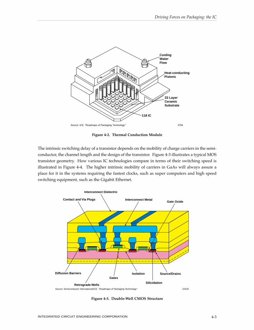
the heat. Multichip module technology was pioneered to Òre-integrateÓ some of the density lost
to the fabrication technology. An example of the IBM 3083 MCM, the Thermal Conduction
Module, or TCM, is shown in Figure 4-2. Because of the higher integration levels and improved
switching speeds of deep submicron CMOS, most mainframe computer systems of the mid- and
late-1990s are based on CMOS technology.
Driving Forces on Packaging: the IC
INTEGRATED CIRCUIT ENGINEERING CORPORATION4-2
Per
cen
t o
f T
ota
l Lo
gic
Mar
ket
*Includes 1% for GaAs
51%
8%
18%
23%
100
90
80
70
60
50
40
30
20
10
0
27%
8%
10%
55%
2%
5% 3%
4%
4%
3%
6%<1%
<1%
88%*
<1%
93%*
91%*
12875Q
TTL and Other Bipolar
ECL
NMOSCMOS
BiCMOS
Source: ICE, "Roadmaps of Packaging Technology"
1982$3.3B
1987$11.6B
1996$24.0B(EST)
2001$54.1B(FCST)
1997$26.7B(FCST)
Figure 4-1. Logic Market Trends by Technology
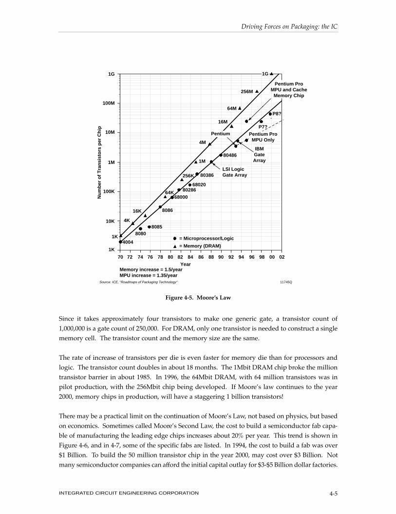
The intrinsic switching delay of a transistor depends on the mobility of charge carriers in the semi-
conductor, the channel length and the design of the transistor. Figure 4-3 illustrates a typical MOS
transistor geometry. How various IC technologies compare in terms of their switching speed is
illustrated in Figure 4-4. The higher intrinsic mobility of carriers in GaAs will always assure a
place for it in the systems requiring the fastest clocks, such as super computers and high speed
switching equipment, such as the Gigabit Ethernet.
Driving Forces on Packaging: the IC
INTEGRATED CIRCUIT ENGINEERING CORPORATION 4-3
CoolingWaterFlow
Heat-conductingPistons
33 LayerCeramicSubstrate
118 IC
3794Source: ICE, "Roadmaps of Packaging Technology"
Figure 4-2. Thermal Conduction Module
Figure 4-3. Double-Well CMOS Structure
Interconnect Dielectric
Contact and Via Plugs Interconnect MetalGate Oxide
Source/DrainsIsolationGates
Diffusion Barriers
Retrograde WellsSilicidation
Source: Semiconductor International/ICE, "Roadmaps of Packaging Technology" 22420

In addition to GaAs, other materials qualify as candidates for the fastest semiconductors, such as
Germanium doped silicon and GaInAs heterojunction structures. However, with their higher
speed comes higher power dissipation, lower integration density and higher costs.
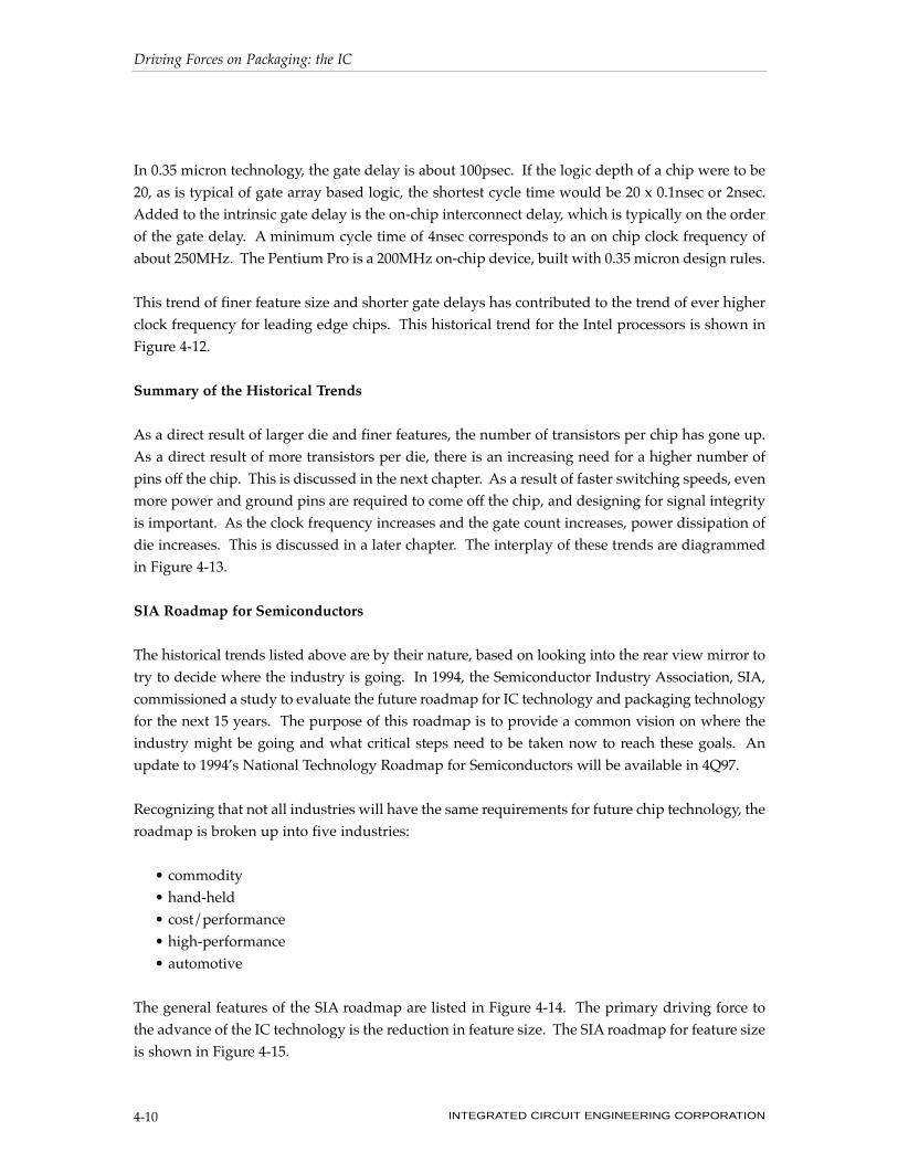
MooreÕs Law and Feature Size Reduction
The relentless year after year advance in the delivered performance of IC devices is due primarily
to two trends: the increasing number of transistors per die and the increading clock frequency. The
number of transistors per die, at the high end of what is in volume production, doubles approxi-
mately every two years. This observation was first pointed out by Gordon Moore, one of the
founders of Intel Corp, and has been termed MooreÕs Law. It is illustrated in Figure 4-5, tracking
the transistor count on Intel processors and DRAM devices.
The Intel 486 processor broke the million transistor per chip barrier in 1990. The Pentium
Processor has about 4 million transistors. The Sun Microsystems UltraSparc, released to volume
production in late 1995, has about 10 million transistors. ASICs from LSI, for example, have over
10 million transistors. If MooreÕs law continues, by the year 2000, the estimate is for logic chips
with more than 50 million transistors per chips.
Driving Forces on Packaging: the IC
INTEGRATED CIRCUIT ENGINEERING CORPORATION4-4
Feature Size (microns)
.1 1 10 100
.001
.01
.1
1
10
100
Sw
itch
ing
Tim
e (n
sec)
CMOS
ECL
GaAs
HEMT
12820ASource: ICE, "Roadmaps of Packaging Technology"
Figure 4-4. Intrinsic Switching Speeds of Selected IC Technologies
Since it takes approximately four transistors to make one generic gate, a transistor count of
1,000,000 is a gate count of 250,000. For DRAM, only one transistor is needed to construct a single
memory cell. The transistor count and the memory size are the same.
The rate of increase of transistors per die is even faster for memory die than for processors and
logic. The transistor count doubles in about 18 months. The 1Mbit DRAM chip broke the million
transistor barrier in about 1985. In 1996, the 64Mbit DRAM, with 64 million transistors was in
pilot production, with the 256Mbit chip being developed. If MooreÕs law continues to the year
2000, memory chips in production, will have a staggering 1 billion transistors!
There may be a practical limit on the continuation of MooreÕs Law, not based on physics, but based
on economics. Sometimes called MooreÕs Second Law, the cost to build a semiconductor fab capa-
ble of manufacturing the leading edge chips increases about 20% per year. This trend is shown in
Figure 4-6, and in 4-7, some of the specific fabs are listed. In 1994, the cost to build a fab was over
$1 Billion. To build the 50 million transistor chip in the year 2000, may cost over $3 Billion. Not
many semiconductor companies can afford the initial capital outlay for $3-$5 Billion dollar factories.
Driving Forces on Packaging: the IC
INTEGRATED CIRCUIT ENGINEERING CORPORATION 4-5
100M
1M
1K
100K
70 72 74 76 78 80 82 84 86 88 90 92 94 00 02
256K
Year
Nu
mb
er o
f T
ran
sist
ors
per
Ch
ip
Memory increase = 1.5/yearMPU increase = 1.35/year
11745QSource: ICE, "Roadmaps of Packaging Technology"
10K
10M
68000
4004
4K
80808085
16K
64K
6802080286
16M
64M
LSI LogicGate Array
4M
1M80486
80386
8086
= Microprocessor/Logic
= Memory (DRAM)
1G
Pentium ProMPU Only
1G
96 98
P7?
P8?
1K
256M
Pentium ProMPU and Cache
Memory Chip
IBMGateArray
Pentium
Figure 4-5. MooreÕs Law

Driving Forces on Packaging: the IC
INTEGRATED CIRCUIT ENGINEERING CORPORATION4-6
1
10
100
1,000
10,000
'66 '74 '82 '90 '98 2003
Source:Forbes/ICE, "Roadmaps of Packaging Technology" 22078Year
Do
llars
in M
illio
ns
Figure 4-6. Cost of Semiconductor Factories (MooreÕs Second Law)
Figure 4-7. New $500 Million+ Fabs in the U.S.
AMD
Cirent (Cirrus/Lucent)
Dominion (IBM/Toshiba)
Fujitsu
Hyundai
Intel
Intel
Intel
Intel
LSI Logic
Matsushita
Motorola
National
NEC
Oki
Samsung
SGS-Thomson
Texas Instruments
Texas Instruments
TwinStar (TI/Hitachi)
WaferTech (TSMC)
White Oak (Motorola/Siemens)
1,300
600
1,200
900
1,300
735
500
1,300
1,350
800
600
1,000
600
1,100
700
1,500
600
600
1,600
500
1,300
1,500
Austin
Orlando
Manassas
Gresham
Eugene
Hillsboro
Santa Clara
Chandler
Rio Rancho
Gresham
Puyallup
Austin
South Portland
Roseville
Tualatin
Austin
Phoenix
Dallas
Dallas
Richardson
Camas
Richmond
Texas
Florida
Virginia
Oregon
Oregon
Oregon
California
Arizona
New Mexico
Oregon
Washington
Texas
Maine
California
Oregon
Texas
Arizona
Texas
Texas
Texas
Washington
Virginia
Fab 25
—
—
Building 2
Fab E4
Fab D1B
Fab D2
Fab 12
Fab 11.2
—
—
MOS 13
—
—
—
Fab 10
—
DMOS-5
DMOS-6
—
—
—
1995
1997
1997
1997
1997
1998
1996
1996
1995
1997
1998
1995
1997
1996
1996
1998
1995
1995
1997
1996
1998
1998
MPU, Logic, Flash
ASIC, MPR
DRAM
DRAM
DRAM
MPU
MPU
MPU
MPU, Logic
ASIC, ASSP
DRAM, MCU
MPU, SRAM
Linear
DRAM
DRAM, ASIC
DRAM, ASIC
MPU, MPR, EPROM
DSP, MPU
DSP
DRAM
Foundry
DRAM
Company Cost ($M) City State Fab Name Year Products
Source: ICE, "Roadmaps of Packaging Technology" 22079

MooreÕs Law is a trend of the high end production capability. These costs do not apply to all fabs.
However, with the equally unrelenting demands for more and faster information processing,
transmission and storage from the end users, it is assured that what was last yearÕs high end tech-
nology will represent mainstream technology next year.
MooreÕs Law has held true for the last 26 years it has been tracked. This treadmill like advance is
made possible by the decrease in transistor size and the increase in yielded die size. The smallest
feature size of a transistor, typically the channel length, is termed the critical dimension or CD.
The current state of the art in lithography technology limits the finest CD possible, at acceptable
yield. As the lithography capability improves, the CD decreases. The underlying enabling tech-
nology for the steady drop of feature size in MooreÕs Law is the increasingly heroic efforts of lith-
ography tools to pattern these smaller dimensions. A significant part of the billion dollar fab cost
is the $100 million lithography toolset cost needed to print 0.35 micron features. Figure 4-8 illus-
trates the historic trend of ever decreasing CD possible on an IC.
Die Area Trends
In addition to the feature size reduction trend, the second trend contributing to MooreÕs Law is the
increase in yielded die size. This historical trend is shown in Figure 4-9. Die area for logic and
memory are increasing at about 13% per year. In 1996, high end chips in volume production were
about 500,000 sq. mils, or 18mm on a side. This feature corresponds to the largest available mask
reticle or opening that can be imaged with state of the art lithography tools. A comparable DRAM
chip was about 300,000mils2 or about 20mm x 10mm.
If this trend continues, dice over 1.25 inches on a side will be in volume production by the year 2000.
Driving Forces on Packaging: the IC
INTEGRATED CIRCUIT ENGINEERING CORPORATION 4-7
0.1
0.2
0.5
1.0
2.0
1984 1986 1988 1990 1992 1994 1996 1998 2000
Fiscal Year19170ASource: Toshiba/JEE/ICE, "Roadmaps of Packaging Technology"
Des
ign
Ru
le (
µm)
DRAMToshiba's gate array
1M-BitDRAM
4M-Bit DRAM
16M-Bit DRAM
64M-Bit DRAM
TC110G
TC140G
TC160G
TC180G
TC200GTC220G
Figure 4-8. Transition of the DRAM and ToshibaÕs Gate Array Development

Gate Delay Trends
In an FET (field effect transistor) structure, the channel length is the distance a charge carrier must
travel from the source to the drain. The transit time for this distance represents the fundamental
delay time for the switching of the transistor. The shorter the distance, the shorter time it will take
for the device to switch. In addition, the faster the mobility of the charge carrier, the shorter the
delay time. With a higher charge carrier mobility than silicon, GaAs and GaAlAs based FETs have
intrinsically shorter gate delays.
As a direct result of reduced feature size, the switching delay for a single gate has historically
decreased. This is shown in Figure 4-10. It is really the trend in smaller feature size that con-
tributes to the shorter delay times and higher clock frequencies possible. Gate delay as a function
of CD is shown in Figure 4-11.
Driving Forces on Packaging: the IC
INTEGRATED CIRCUIT ENGINEERING CORPORATION4-8
1,000
100
10
60
70 72 74 76 78 80 82 84 86 88 90 92 94 96 98
Pentium
80486
8038668020
8028668000
8086
Z80
8080
4K
16K
256K
1M
4M
16M
64M
1G
= Microprocessor/Logic
= Memory
Year
Ch
ip A
rea
(Th
ou
san
ds
of
sq m
ils)
64K
Memory increase = 1.13/yearMPU increase = 1.13/year
11746QSource: Intel/ICE, "Roadmaps of Packaging Technology"
20
40
80
600
200
400
800
P54C
00 02
P8?
R4000
2,000
256M
IBMGate Array
Pentium ProMPU and Cache
PentiumPro
MPUOnly
P7?
Figure 4-9. IC Die Size Trends

Driving Forces on Packaging: the IC
INTEGRATED CIRCUIT ENGINEERING CORPORATION 4-9
80 81 82 83 84 85 86 87 88 89 90 91 92 93 94 960.01
0.1
1
10
Mic
ron
s
Year
1990 Forecasted CommercialLimit For Optical Lithography (0.35µ)
= Laboratory Reasearch
MIT (0.06µ)X-Ray
Bell Labs(0.14µ)
Toshiba(0.25µ) IBM
(0.25µ)Gate Array
(X-Ray)
Loose Production ResolutionTight Production Resolution
Development
HMOS II(2.0µ)
HMOS IV(1.0µ) 4M DRAM
(0.8µ)16M DRAM
(0.5µ)64M DRAM
(0.35µ)
256K DRAM(1.6µ) 1M DRAM
(1.2µ)
16M DRAM(0.5µ)
64M DRAM(0.35µ)
4M DRAM(0.8µ)
WE 3210032-Bit MPU
(1.5µ)
10981QSource: ICE, "Memory 1997"
95
256MDRAM(0.25µ)
256MDRAM(0.25µ)
1992 Forecasted CommercialLimit For Optical Lithography (0.15µ)
97
1G DRAM(0.15µ)
Toshiba(0.1µ)
Toshiba(0.04µ)
98 0200
(2.0µ)
(1.0µ)
(0.7µ)
4GDRAM(0.08µ)
1GDRAM(0.15µ)
1996 Forecasted CommercialLimit for Optical Lithography (0.1µ)
Figure 4-10. IC Feature Size Trends
Figure 4-11. Low Power Speed Lag
0.1
0.2
0.3
0.4
0.5
0.6
0.7
0.80.91.0
35
70
105
140
175
210
245
280315350
Gat
e D
elay
(A
rbit
rary
Un
its)
Un
load
ed In
vert
er D
elay
(p
s)
2µm 1µm 0.5µm 0.25µm 0.13µm
Speed Doubles Every2 Generations
Speed Doubles Every4 Generations
3.3V
3.3V
2.2V
2.2V
1.5V
(Low Power)
(High Speed)
5V
Technology Generation19499Source: ISSCC94/UC Berkeley/ICE, "Roadmaps of Packaging Technology"
In 0.35 micron technology, the gate delay is about 100psec. If the logic depth of a chip were to be
20, as is typical of gate array based logic, the shortest cycle time would be 20 x 0.1nsec or 2nsec.
Added to the intrinsic gate delay is the on-chip interconnect delay, which is typically on the order
of the gate delay. A minimum cycle time of 4nsec corresponds to an on chip clock frequency of
about 250MHz. The Pentium Pro is a 200MHz on-chip device, built with 0.35 micron design rules.
This trend of finer feature size and shorter gate delays has contributed to the trend of ever higher
clock frequency for leading edge chips. This historical trend for the Intel processors is shown in
Figure 4-12.
Summary of the Historical Trends
As a direct result of larger die and finer features, the number of transistors per chip has gone up.
As a direct result of more transistors per die, there is an increasing need for a higher number of
pins off the chip. This is discussed in the next chapter. As a result of faster switching speeds, even
more power and ground pins are required to come off the chip, and designing for signal integrity
is important. As the clock frequency increases and the gate count increases, power dissipation of
die increases. This is discussed in a later chapter. The interplay of these trends are diagrammed
in Figure 4-13.
SIA Roadmap for Semiconductors
The historical trends listed above are by their nature, based on looking into the rear view mirror to
try to decide where the industry is going. In 1994, the Semiconductor Industry Association, SIA,
commissioned a study to evaluate the future roadmap for IC technology and packaging technology
for the next 15 years. The purpose of this roadmap is to provide a common vision on where the
industry might be going and what critical steps need to be taken now to reach these goals. An
update to 1994Õs National Technology Roadmap for Semiconductors will be available in 4Q97.
Recognizing that not all industries will have the same requirements for future chip technology, the
roadmap is broken up into five industries:
¥ commodity
¥ hand-held
¥ cost/performance
¥ high-performance
¥ automotive
The general features of the SIA roadmap are listed in Figure 4-14. The primary driving force to
the advance of the IC technology is the reduction in feature size. The SIA roadmap for feature size
is shown in Figure 4-15.
Driving Forces on Packaging: the IC
INTEGRATED CIRCUIT ENGINEERING CORPORATION4-10

Driving Forces on Packaging: the IC
INTEGRATED CIRCUIT ENGINEERING CORPORATION 4-11
1970 1975 1980 1985 1990 200019950.1
0.2
0.3
0.4
0.5
0.7
1.0
2
3
45
7
10
20
30
40
50
70
100
200
300
400
500
700
1,000
4004 108KHz (0.06 MIPS)
8008 200KHz (0.06 MIPS)
8080 2MHz (0.64 MIPS)
8085 5MHz (0.37 MIPS)
8086 10MHz (0.75 MIPS)
80286 12MHz (2.66 MIPS)
Intel 386DX 16MHz (6 MIPS)
Intel 486DX33MHz (27 MIPS)
Pentium 66MHz(112 MIPS)
Intel 386DX 20MHz (7 MIPS)
Intel 386DX 25MHz (8.5 MIPS)
Intel 386DX 30MHz (11.4 MIPS)
Intel 486DX 50MHz (41 MIPS)
Per
form
ance
(M
Hz)
Year
19062BSource: ICE, "Roadmaps of Packaging Technology"
P6* 100MHz(300 MIPS)
Pentium Pro 200MHz (600 MIPS)
*ICE estimate
Figure 4-12. Intel MPU Performance Trends

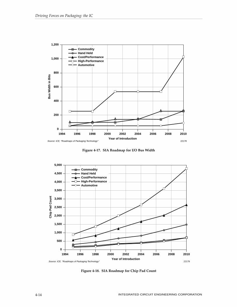
The future expectations for the IC and packaging industry are illustrated in the following plots of:
¥ chip size (Figure 4-16)
¥ I/O bus width (Figure 4-17)
¥ chip pad pin count (Figure 4-18)
¥ package pin count (Figure 4-19)
¥ on-chip clock frequency (Figure 4-20)
¥ chip to board clock frequency (Figure 4-21)
¥ core voltage (Figure 4-22)
¥ single chip power dissipation (Figure 4-23)
¥ cost/pin (Figure 4-24)
Driving Forces on Packaging: the IC
INTEGRATED CIRCUIT ENGINEERING CORPORATION4-12
Feature Size (µm)
Gates/Chip
Bits/Chip
Chip Size (mm2)
Wafer diameter (mm)
Number of interconnect levels (logic)
Max. Power (W/Die)
Power Supply (V)
Number of I/Os
Performance (MHz)
• DRAM
• SRAM
• Logic/Microprocessor
• DRAM
• High-performance
• Portable
• Off-chip
• On-chip
1995 1998 2001 2004 2007
0.35
800K
64M
16M
400
200
200
4-5
15
2.2
750
100
200
0.25
2M
256M
64M
600
320
200-400
5
30
2.2
1,500
175
350
0.18
5M
1G
256M
800
500
200-400
5-6
40
1.5
2,000
250
500
0.12
10M
4G
1G
1,000
700
200-400
6
40-120
1.5
3,500
350
700
0.10
20M
16G
4G
1,250
1,000
200-400
6-7
40-200
1.5
5,000
500
1,000
Source: Semiconductor Industry Association/EET/ICE, "Roadmaps of Packaging Technology" 18624
Figure 4-14. SIAÕs Technology Roadmap
Source: ICE, "Roadmaps of Packaging Technology" 22545
IC Technology DrivesIC TechnologyConsequences
Impact for PackagingTechnology
• larger yielded die size
• shorter gate lengths
• more transistors per die
• shorter gate delay
• higher clock frequency
• higher power dissipation
• higher I/O count required
• signal integrity featuresrequired
• interconnect delays tobe minimized
• more efficient thermalmanagement required
Figure 4-13. IC Technology Trends

Driving Forces on Packaging: the IC
INTEGRATED CIRCUIT ENGINEERING CORPORATION 4-13
0.35
0.3
0.25
0.2
0.15
0.1
0
1994 1996 1998 2000 2002 2004 2006 2008 2010
Fea
ture
Siz
e (m
icro
n)
Year of IntroductionSource: ICE, "Roadmaps of Packaging Technology" 22176
1,400
1,200
1,000
800
600
400
200
0
1994 1996 1998 2000 2002 2004 2006 2008 2010
Ch
ip A
rea
(mm
2 )
Year of IntroductionSource: ICE, "Roadmaps of Packaging Technology" 22177
CommodityHand HeldCost/PerformanceHigh-PerformanceAutomotive
Figure 4-15. SIA Roadmap for Feature Size Reduction
Figure 4-16. SIA Roadmap for Chip Area
Driving Forces on Packaging: the IC
INTEGRATED CIRCUIT ENGINEERING CORPORATION4-14
1,200
1,000
800
600
400
200
0
1994 1996 1998 2000 2002 2004 2006 2008 2010
Bu
s W
idth
in B
its
Year of IntroductionSource: ICE, "Roadmaps of Packaging Technology" 22178
CommodityHand HeldHigh-PerformanceAutomotive
CommodityHand HeldCost/PerformanceHigh-PerformanceAutomotive
5,000
4,500
4,000
3,500
3,000
2,500
2,000
1,500
1,000
500
0
1994 1996 1998 2000 2002 2004 2006 2008 2010
Ch
ip P
ad C
ou
nt
Year of IntroductionSource: ICE, "Roadmaps of Packaging Technology" 22179
CommodityHand HeldCost/PerformanceHigh-PerformanceAutomotive
Figure 4-17. SIA Roadmap for I/O Bus Width
Figure 4-18. SIA Roadmap for Chip Pad Count

Driving Forces on Packaging: the IC
INTEGRATED CIRCUIT ENGINEERING CORPORATION 4-15
5,000
4,500
4,000
3,500
3,000
2,500
2,000
1,500
1,000
500
0
1994 1996 1998 2000 2002 2004 2006 2008 2010
Pac
kag
e P
ins
Year of IntroductionSource: ICE, "Roadmaps of Packaging Technology" 22180
CommodityHand HeldCost/PerformanceHigh-PerformanceAutomotive
2,000
1,800
1,600
1,400
1,200
1,000
800
600
400
200
0
1994 1996 1998 2000 2002 2004 2006 2008 2010
Clo
ck F
req
uen
cy (
MH
z)
Year of IntroductionSource: ICE, "Roadmaps of Packaging Technology" 22181
CommodityHand HeldCost/PerformanceHigh-PerformanceAutomotive
Figure 4-19. SIA Roadmap for Package Pin Count
Figure 4-20. SIA Roadmap for On-Chip Clock Frequency

Driving Forces on Packaging: the IC
INTEGRATED CIRCUIT ENGINEERING CORPORATION4-16
2,000
1,800
1,600
1,400
1,200
1,000
800
600
400
200
0
1994 1996 1998 2000 2002 2004 2006 2008 2010
Clo
ck F
req
uen
cy (
MH
z)
Year of IntroductionSource: ICE, "Roadmaps of Packaging Technology" 22182
CommodityHand HeldCost/PerformanceHigh-PerformanceAutomotive
6
5
4
3
2
1
0
1994 1996 1998 2000 2002 2004 2006 2008 2010
Vo
ltag
e (v
olt
s)
Year of IntroductionSource: ICE, "Roadmaps of Packaging Technology" 22183
CommodityHand HeldCost/PerformanceHigh-PerformanceAutomotive
Figure 4-21. SIA Roadmap for Chip to Board Clock Frequency
Figure 4-22. SIA Roadmap for Core Voltage

Driving Forces on Packaging: the IC
INTEGRATED CIRCUIT ENGINEERING CORPORATION 4-17
180
160
120
140
100
80
60
40
20
0
1994 1996 1998 2000 2002 2004 2006 2008 2010
Po
wer
Dis
sip
atio
n (
wat
ts)
Year of IntroductionSource: ICE, "Roadmaps of Packaging Technology" 22184
CommodityHand HeldCost/PerformanceHigh-PerformanceAutomotive
18
16
12
14
10
8
6
4
2
0
1994 1996 1998 2000 2002 2004 2006 2008 2010
Co
st P
er P
in (
$0.0
1/p
in)
Year of IntroductionSource: ICE, "Roadmaps of Packaging Technology" 22185
CommodityHand HeldCost/PerformanceHigh-PerformanceAutomotive
Figure 4-23. SIA Roadmap for Power Dissipation
Figure 4-24. SIA Roadmap for High End of Package Costs

As is apparent from these roadmaps, to keep up with the expectations of the end users and the IC
technology that may be in place over the next 15 years, the packaging industry must run at least
twice as fast as ever before, just to stay in the same place.
Figures of Merit; Speed-Power Product
A number of figures of merit have been developed to facilitate comparisons among technologies
and generations. One of these is the speed-power product, which is the product of the gate prop-
agation delay, tgate delay, and the power dissipation per gate, Pgate. It is a rough measure of the
energy switched in each gate per logic transition, measured in joules. As the switching frequency
increases, the speed-power product is a better measure of the energy associated with one bit. The
power dissipation per gate can be estimated from the total number of gates, Ngates, and the total
power dissipation of the chip, Pchip:
The speed-power product is:
In each logic swing, this energy will always be converted into heat and contributes to the chipÕs
power dissipation. The lower the speed-power product, the faster the switching per watt of
power dissipated.
The intrinsic properties of various device technologies are shown in Figure 4-25.
Figures of Merit; Computational Capacity and Clock Frequencies
Incorporating into a figure of merit the influence of the rate at which a gate switches can lead to
ambiguities. There are two frequencies that might be used, the maximum toggle frequency,
Ftoggle, or the maximum clock frequency, Fclock. They are not the same.
The toggle frequency is unambiguous. The maximum toggle frequency for an individual gate is
a measure of how it would behave in a ring oscillator. The switching frequency is limited by the
two propagation delays per cycle, corresponding to the high-to-low and low-to-high transitions:
F
12 ttoggle
gate delay
=•
speed power product
t P
Ngatedelay chip
gates
− =•
P
P
Ngatechip
gates
=
Driving Forces on Packaging: the IC
INTEGRATED CIRCUIT ENGINEERING CORPORATION4-18

In a microprocessor, where the logic architecture and connections are established and well
defined, both the maximum toggle frequency and the maximum clock frequency at which the chip
will run are also well defined and related by the logic depth.
A signal must propagate sequentially through a number of logic gates in one clock period, tclock.
The number of sequential gates is called the logic depth, Nlogic depth. The clock period must be
long enough to allow the signal to propagate through all the gates:
For a 16MHz clock frequency or 62nsec clock period, such as for a vintage 80386 device, the gate
delay is 2.5nsec. The logic depth is calculated to be 25. With a 2.5nsec gate delay, the toggle fre-
quency would be 200MHz. In this example, the clock frequency is eight percent of the toggle
frequency.
In a 200MHz Pentium Pro, the cycle time is 5nsec. With a logic depth of 20, the intrinsic gate delay
is 0.25nsec. The toggle frequency for the transistors would be 2GHz.
t N tclock logic depth gate delay> •
Driving Forces on Packaging: the IC
INTEGRATED CIRCUIT ENGINEERING CORPORATION 4-19
1µW 10µW 100µW 1mW 10mW 100mW
10ns
1ns
100ps
10ps
1ps
CMOSSOS Si
CMOS
SiNMOS
SiECL
GaAsE/D
GaAsMESFET
GaAsHEMT
Gat
e P
rop
agat
ion
Del
ay
Power Dissipation/Gate
100pJ10pJ
1pJ
100fJ
10fJ1fJ0.1fJ0.01fJ
15791Source: National Semiconductor Corporation/ICE, "Roadmaps of Packaging Technology"
Figure 4-25. Technology Speed-Power Curve

As a rule of thumb, the toggle frequency is roughly 10x the clock frequency, which corresponds to
a logic depth of 20. Without knowing the specific logic architecture, 20 is a good approximation
of the logic depth.
In an ASIC gate array, there is no a priori clock frequency. The design of the logic architecture will
determine the logic depth. However, it has become conventional to use a number of the order of
20 as the logic depth. In specific cases, when the clock frequency is known, this value should be
used instead.
Figures of Merit; Computational Capacity
The product of the number of gates on the chip and the maximum clock frequency is a rough mea-
sure of the available computational capacity, in units of gate-Hz, given by:
The computational capacity for a 16MHz 386 processor is 16MHz x 250,000 gates = 4 x 10¹² gate-
Hz. The Pentium Pro, for example has a computational capacity of 200MHz x 1.2 million = 2.4 x
1014 gate-Hz. In just 6 years, from the introduction of the 386 to the P6, the computational capac-
ity has increased by a factor of 50!
Based on the SIA roadmap, the computational capacity for future chips is shown in Figure 4-26.
Computational Capacity N F
N
20 tgates clockgates
gate delay
= • =•
Driving Forces on Packaging: the IC
INTEGRATED CIRCUIT ENGINEERING CORPORATION4-20
1E+18
1E+17
1E+16
1E+15
1E+14
1994 1996 1998 2000 2002 2004 2006 2008 2010
Co
mp
uta
tio
nal
Cap
acit
y (g
ate-
Hz)
Year of IntroductionSource: ICE, "Roadmaps of Packaging Technology" 22186
Pentium Pro
Figure 4-26. SIA Roadmap for Computational Capacity
Figures Of Merit; Functional Throughput Rate (FTR)
Functional throughput rate (FTR) is a measure of the available computation density on the chip.
With Achip referring to the area of the chip, the FTR density, in units of gate-Hz/cm2, is:
Because FTR can apply to all levels of the system, the normalizing area should be specified so as
to not add ambiguity.
The FTR has become a popular figure of merit for device complexity. The VHSIC programs of
1990 were directed toward meeting FTR goals.
For Phase I, the FTR goal was 5 x 10¹¹ gate-Hz/cm2.
For Phase II, the FTR goal was 1 x 10¹³ gate-Hz/cm2.
These values should be compared with the FTR demonstrated by gate arrays in ECL and CMOS
technologies available in 1991:
Motorola MCAIII (ECL): FTR = 0.63 x 10¹³ gate-Hz/cm2
Toshiba TC140G (CMOS): FTR = 0.96 x 10¹³ gate-Hz/cm2
They are both able to approximate the VHSIC Phase II goals. ECL uses raw speed, while CMOS
gains from integration density.
The FTR of 200MHz Pentium technology is roughly 1,200,000 gates x 200MHz / 2 cm2 = 12 x 1013
gate-Hz/cm2.
Based on the advances in gate count, chip size and clock frequency, from the SIA roadmap, the
FTR of future chips is shown in Figure 4-27.
METRICS FOR PACKAGE-LIMITED PERFORMANCE
System Level Constraints
An information appliance product is defined by its form factor. This places constraints in terms
of physical size, power consumption and cost. The goal of successful design is to produce a prod-
uct meeting the size, power and cost constraints, while achieving the required performance level,
in an ever shortening access window of time to market.
FTR
Computational CapacityA
N F
A
N
A 20 tchipchip
gates clock
chip
gates
chip gate delay
= =•
=• •
Driving Forces on Packaging: the IC
INTEGRATED CIRCUIT ENGINEERING CORPORATION 4-21

At the very highest performance end, the final product is graded on its total performance, with
cost being a close second target. The constraints of size and power are soft. The physical size of
supercomputers and the power they dissipate are secondary factors, and of concern only in how
they affect both the performance and the cost. Technology selections are performance/cost
driven, with a slant toward highest possible performance.
At the smaller end of the form factors, where portability is a feature, the final system is tightly con-
strained by size, power and cost. The technology selections are driven by performance-den-
sity/watt/cost.
In between these extremes is the desktop market, where size is an important constraint, cost is an
important constraint and power is a softer constraint, limited to a plug power of roughly 1,200
watts. For products that plug in the wall, there is a steady push on the system design to get more
performance per volume per unit cost, or performance-density/cost.
The interplay between these driving forces is shown in Figure 4-28. For the majority of systems
that fall in this middle range, the overriding driving force that dictates the technology choice is not
higher performance per se. The driving force is really increased performance density per unit cost.
Driving Forces on Packaging: the IC
INTEGRATED CIRCUIT ENGINEERING CORPORATION4-22
1E+17
1E+16
1E+15
1E+14
1991 1993 1995 1997 1999 2001 2003 20072005 2009 2011
FT
R (
gat
e-H
z/cm
2 )
Year of IntroductionSource: ICE, "Roadmaps of Packaging Technology" 22187
Pentium Pro
Figure 4-27. SIA Roadmap for Functional Throughput Rate (FTR)

To evaluate a particular set of technology choices, it is important to look at how they will impact
the performance density per unit cost of the system. At the larger form factor, raw performance
is the weighting factor, and at the smaller form factor, performance density/watt/cost is the
weighting factor.
Packaging Efficiency
MIPS is a metric used to describe the performance of a computer. It is fundamentally related to
the number of gates that can communicate in one clock cycle. It does not relate to the technology
used to implement the performance. A few new metrics have been invented to provide a relative
measure of the packageÕs capability of delivering varying degrees of performance-density/cost.
Packaging efficiency, η, is a measure of how densely packed the silicon is, at the package level, the
module level, the board level, or the system level. In general, for planar surfaces it is the ratio of
the area of the silicon to the area of the package:
η =
A
Achip
package
Driving Forces on Packaging: the IC
INTEGRATED CIRCUIT ENGINEERING CORPORATION 4-23
Watch PDA LaptopComputer
PersonalComputer
Workstation Server MainframeComputer
SuperComputer
Per
form
ance
Performance Density/Watt/$
Performance Density/$
Raw Performance/$
Migration of supercomputerperformance into shirt pocket
Form FactorSizePrice
15789ASource: ICE, "Roadmaps of Packaging Technology"
Figure 4-28. Relative Performance Versus Product Form Factors

When applied to a package, the packaging efficiency is a measure of how much of the surface area
is silicon. Imagine removing the lid or encapsulant on a package, and looking at the size of the pack-
age compared to the silicon. Figure 4-29 is an example of a DIP package with the chip inside, show-
ing the relatively small size of the chip, compared to the package size.
There are five aspects of the packaging choices that can limit packaging efficiency.
1. The I/O format of the chip
2. The I/O format of the package
3. The via density of the substrate
4. The interconnect density of the substrate
5. The thermal management of the substrate
The less able the package is to efficiently address these issues, the farther apart the chips must be
mounted on the substrate and the lower the packaging efficiency. In general, the farther apart the
die, the higher the cost of the system, due to larger board area, enclosure size and system weight.
For single-chip packages on a printed circuit board, it is usually the I/O format of the package that
limits the packaging efficiency. For example, a pad limited ASIC having 4mil peripheral pad
pitch, packaged in a PQFP with 25mil peripheral pitch has a packaging efficiency of (4/25)2 =
2.6%. This means that if these packages were laid out completely covering a board, less than 3%
of the board would actually have silicon on it. The other 97% of the board area would be devoted
to increasing the size of the system, increasing the weight of the system, decreasing the clock fre-
quency and increasing its cost.
Driving Forces on Packaging: the IC
INTEGRATED CIRCUIT ENGINEERING CORPORATION4-24
Source: ICE, “Roadmaps of Packaging Technology” 22572
Figure 4-29. Typical DIP With Lid Exposed Showing the Chip Size Compared With the Package Size

For printed circuit board based chip-on-board (COB), the via density and interconnect density
limit how close together the dice can be placed. This has spurred the introduction of new sub-
strates for COB, such as cofired ceramic and thin-film multilayer substrates, which use blind and
buried vias, having more than 10x the via and interconnect density of plated through-hole boards.
Practical air cooling can remove about 10W/in2. For very high power chips, enough surface area
must be available for the heat sinks. For example, using 35 watt ECL chips, each about 0.35 inch
on a side, the maximum packaging efficiency possible is less than four percent. Large heatsinks
or liquid cooling is needed to get significantly higher packaging efficiency.
Packaging efficiency is a measure of the density of the gates on the board surface. It is also a good
measure of the efficiency of the interconnect substrate. A higher packaging efficiency means the
chips are closer together, interconnect delays are minimized, and the package and interconnects
minimally reduce the clock frequency.
Simple Models For Packaging Requirements And Constraints
ÒHarvard students learn less and less about more and more and end up knowing nothing
about everything.Ó
ÒMIT students learn more and more about less and less and end up knowing everything about
nothing.Ó
Ñanonymous
Between the wishes of the system designers for higher performance density at lower cost, and the
advancing capabilities of IC technology trying to satisfy these requirements, are the constraints
imposed by the package and interconnects.
The reduction in gate feature size means a decrease in propagation delay and an increase in the
bandwidth of signals that must propagate. The increase in number of gates per die means more
I/O pins are required, which means an increase in the interconnect density required and an
increase in the total power dissipated by the chip.
The direct relationships between the IC advances and the driving forces on the packaging tech-
nology are diagrammed in Figure 4-30. As long as IC technology continues to improve, the pack-
age must run faster and faster just to stay in the same place.
Driving Forces on Packaging: the IC
INTEGRATED CIRCUIT ENGINEERING CORPORATION 4-25

In order to gain insight that can be used to identify real constraints and point the direction toward
solutions, simple models must be introduced. The more general they are, the greater the range of
technologies and applications to which they will apply. However, the less technical validity they
will have for any one specific case.
Such simple models may provide a framework for deciding among the incredibly wide variety of
packaging options, while quantitatively evaluating their tradeoffs.
Later in this book, we introduce a series of approximations that seek to balance generalities with
specific examples to offer insights for the underlying requirements on the constraints imposed by
the package. They are not meant to be all encompassing, nor exact. The real purpose of these
simple models is to provide a quantitative foundation for our intuitive understanding of the
interplay among the driving forces and the possible solutions. Where appropriate, specific exam-
ples of current devices are used to estimate realistic values. It is always important to keep in mind
that ÒcurrentÓ features of any IC technology are moving targets and will by definition be out of
date in less than two years.
Driving Forces on Packaging: the IC
INTEGRATED CIRCUIT ENGINEERING CORPORATION4-26
ICTechnologyAdvances
IC TechnologyRequirements
SystemIssues
PackagingConstraints
DecreasingTransistor Size
IncreasingYield
Shorter PropagationDelay
Higher Higher
SignalBandwidth
Lower Lower
NoisePower
DissipationNumber
of I/O
More GatesPer Die
LargerDie
ClockFrequency
Higher
Lower Higher
Lower
Higher
Lower
15792Source: ICE, "Roadmaps of Packaging Technology"
Figure 4-30. IC Technology Advances Drive Packaging Advances
SUMMARY OF THE DRIVING FORCES ON PACKAGING
Faster, Denser, Cheaper, Lower Power, NOW
Higher performance means more gates in the system operating at higher clock frequencies.
Higher performance density means a higher gate density switching faster at a lower cost. This is
often referred to as: ÒDenser, Faster, Cheaper.Ó The ultimate limit is set by the IC choices. The
steady, unrelenting advance in chip technologies will forever require the packaging and intercon-
nect technologies to advance in:
1. higher packaging efficiency
2. higher pin count
3. higher via density
4. higher interconnect density
5. higher power density to be removed
6. higher bandwidth interconnects
7. shorter wiring delays
How well the package and interconnect are able to meet these needs is reflected in the resulting
packaging efficiency. In addition to the gate density, the packaging efficiency also reflects some of
the manufacturing costs and the impact on clock frequency. The lower the packaging efficiency,
the longer the total length of the interconnect traces and the higher the substrate costs. Likewise,
the longer the traces, the longer the wiring delays, and the lower the potential clock frequency.
Depending on the political clout of the IC design group, these packaging requests will be called
demands, requirements, needs, or wishes. The less capable the package is at meeting these
wishes, the lower the performance density per unit cost.
Driving Forces on Packaging: the IC
INTEGRATED CIRCUIT ENGINEERING CORPORATION 4-27

Driving Forces on Packaging: the IC
INTEGRATED CIRCUIT ENGINEERING CORPORATION4-28


