
11
AMSE JOURNALS-2017-Series: Advances C; Vol. 72; N°1; pp 11-24
Submitted Sept. 2016; Revised Dec. 12, 2016, Accepted Feb. 15, 2017
A Low Noise and Power Efficient 45nm GPDK Technology based
Highly Stable Current Balancing Logic (HCBL) and Dynamic
Logic Circuits for Mixed Signal Systems *S Seenuvasamurthi,
**G Nagarajan
* Department of ECE, Research Scholar, Pondicherry University,
India, Pondicherry Engineering College, Pondicherry, ([email protected])
** Department of ECE, Professor, Pondicherry University,
India, Pondicherry Engineering College, Pondicherry, ([email protected])
Abstract Noise is an important factor in the analog and digital circuits which determine the
characteristics of the system. There are many sources of noises. Power supply noise caused
by circuit switching, crosstalk noise due to capacitive coupling between neighboring
interconnects, fluctuations in device parameters due to process variations, noise due to charge
sharing and charge leakage in high speed dynamic logic circuits. The work aims at
developing a noise robust circuit with high frequency response. The same circuit can be
implemented in a dynamic logic system with reduced number of transistor. Also the dynamic
logic will have the probability of signal switching activity to be low which will subsequently
reduce the power of the system. The circuits have been constructed using cadence ADE and
the same has been simulated with Spectra using 45nm GPDK technology. The simulation
results show that the power consumption has been reduced multi-fold and the bandwidth has
been increased by 102
Hz and the delay is reduced by 50%
Keywords
Current Balanced Logic, pseudo-NMOS, Noise immunity, Dynamic logic
1. Introduction
Building noise is an important factor in VLSI circuits. Noise is defined as any
deviation of a signal from its nominal value in those sub-intervals of time when it should
otherwise be stable [1]. Noise in digital circuits can be attributed to several sources, such as
power supply noise, charge sharing noise, leakage noise and crosstalk noise. During design,
rigorous noise analysis and noise considerations are becoming increasingly important. The
following trends in modern digital IC design accentuate the need for careful and detailed

12
consideration of noise during circuit design and optimization. Lowering the Supply voltages,
leading to smaller margins for noise; Transistors threshold voltages are being lowered,
leading to higher levels of leakage noise; Circuits are being packed closer together, leading to
increased coupling and crosstalk noise; Signals have faster rise and fall times, leading to
more power supply noise; The increased use of dynamic circuitry for performance reasons
worsens the susceptibility to noise problems.
Charge-sharing noise problems are often avoided by appropriate sizing of transistors.
When a circuit is optimized, in addition to criteria such as delay, power, noise and area
should be considered. The mathematical expression for noise consideration in circuit
optimization is in the form of a non-linear semi-infinite problem [2-3]. Moreover, the number
of signals that must be checked for noise violations and the number of subintervals of time
during which these checks must be performed are potentially large. Hence, the incorporation
of noise considerations during circuit optimization is an arduous task and no practical
solution exists in the literature.
The rest of the paper is described as follows. The section II discuss about the previous
predominant works in this domain. Section III explains about the proposed circuit its
construction, working and the mathematical model for the small signal equivalent. Section
IV discuss about the simulation results and their interpretation. Section V concludes the
work.
2. Previous works
There are many works which has been reported on this noise immunity circuit
building. This work takes a few close references from the Current Balanced Logic (CLB) for
the proposed circuit. Fig.1 achieves ideally constant supply current by using a diverse
principle. They may be regarded as pseudo-NMOS circuits [3], [4] to which transistor M3 has
been added. The aim is that, during logic transitions, the variation of iD3 compensates (or
balances and hence, the designation current balanced logic) the variation of iD2 [5], [6]. It is
observed that a perfect compensation can be obtained, thus making iD3 + iD2 = IDD constant as
shown in Fig. 3, if transistors M2 and M3 are matched.

13
Fig.1. Current Balanced Logic family
Fig.2. Gain improvement circuit
Vtn = Vtp = Vt (1)
K3 = K2 = K (2)
K3 = ½[ μn Cox W3/L3] (3)
K2 = ½[ μp Cox W2/L2] (4)
where, K is the constant, Vtp and Vtn are the threshold voltages of the PMOS and NMOS
transistors, respectively and with the usual meaning for (mobility), Cox (gate oxide
capacitance) and W=L (aspect ratio). It is straight forward to show that iD3 + iD2 = IDD. Thus,
a constant supply current is obtained for all values of VO, to the degree that M2 and M3 are
matched (simulations show that mismatches [7], [8] of up to 10% have little effect on the
amplitude of the supply current spikes). The usage of dynamic logic also improves the power
since it reduces the switching activity of the logic to a great extent. This work aim for
developing a dynamic logic with feedback structure to reduce the leakage loss and transitions
in the output.
14
3. Proposed work
This work aim for developing a circuit with high gain with reduced mismatch so as to
reduce the noise in the circuits. The concept of cascade structure will improve the gain of the
proposed structure and the same will also act as shielding structure for reducing the noise by
reducing the mismatch in the proposed circuit. The same concept can be illustrated by a
mathematical small signal model to show the gain of the proposed structure has improved.
3.1 Gain improvement by cascode
Consider the circuit in Fig.2 with input signal given to MOSFET. It’s known that a
transistor in a common-source arrangement converts a voltage signal to current signal [9].
MOSFET M2 is cascade on the top of M1 which provides many useful properties. In the Fig.2
M1 generates a small signal drain current proportional to Vin and M2 simply routes the current
to RD.
It is notated that, M1 the input device and M2 the cascade device. Note that in this
circuit, M1 and M2 carry equal currents. The attributes of the circuit is described in this
section and many advantages of the cascode structure over a simple common-source stage
become evident. For M1 to operate in saturation Vx ≥ Vin – Vth. If M1 and M2 are both in
saturation, the Vx is determined primarily by
Vx = Vb – Vgs2. Thus,
Vb- Vgs2 ≥ Vin – Vth1 and hence
Vb>Vin + Vgs2 – Vth1. (5)
For M2 to be saturated,
Vout ≥Vb –Vth2, that is
Vout ≥ Vin – Vth1 + Vgs2 – Vgs2 (6)
Equations (5) and (6) provide the necessary biasing condition for getting the high gain
structure. Vb is chosen to place M1 at the edge of saturation [10]. Consequently, the minimum
output level for which both transistors operate in saturation is equal to the overdrive voltage
of M1 plus that of M2. In other words, addition of M2 to the circuit reduces the output voltage
swing by at least the overdrive voltage of M2. M2 is stacked on top of M1 and now analysing
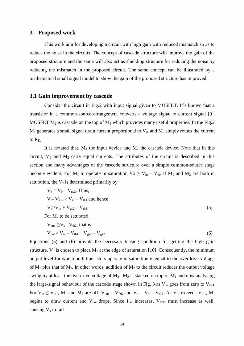
the large-signal behaviour of the cascode stage shown in Fig. 3 as Vin goes from zero to VDD.
For Vin ≤ Vth1, M1 and M2 are off. Vout = VDD and Vx = Vb – Vth2. As Vin exceeds Vth1, M1
begins to draw current and Vout drops. Since ID2 increases, VGS2 must increase as well,
causing Vx to fall.
15
Fig.3. Input output characteristics of a cascode stage
Fig.4. Large signal analysis
As Vin assumes sufficiently large values, two effects occur: (1) Vx drops below Vin by
Vth1, forcing M1 into the triode region; (2) Vout drops below Vb by Vth2, driving M2 into the
triode region. Depending on the device dimensions and the values of RD and Vb, one effect
may occur before the other. For example, if Vb is relatively low, M1 may enter the triode
region first. Note that if M2 goes into deep triode region, Vx and Vout become nearly equal. To
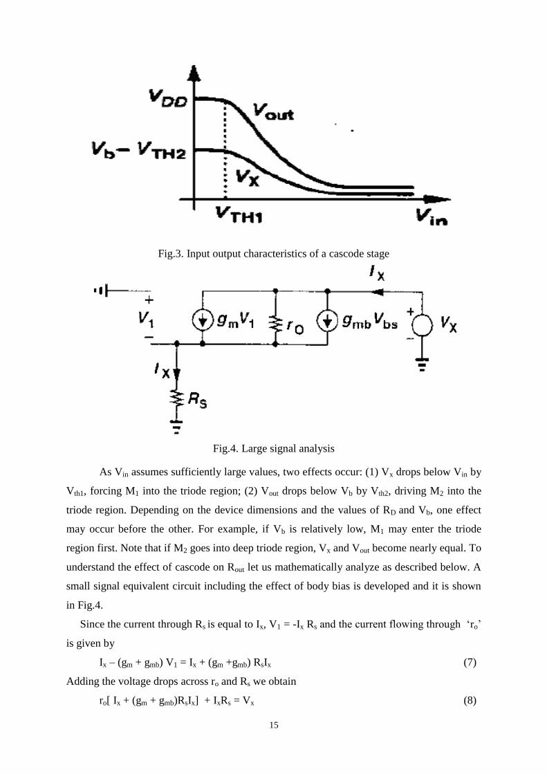
understand the effect of cascode on Rout let us mathematically analyze as described below. A
small signal equivalent circuit including the effect of body bias is developed and it is shown
in Fig.4.
Since the current through Rs is equal to Ix, V1 = -Ix Rs and the current flowing through ‘ro’
is given by
Ix – (gm + gmb) V1 = Ix + (gm +gmb) RsIx (7)
Adding the voltage drops across ro and Rs we obtain
ro[ Ix + (gm + gmb)RsIx] + IxRs = Vx (8)

16
It follows that
Rout = [1 + (gm + gmb)Rs] ro + Rs
= [1+ (gm + gmb)ro]Rs + ro (9)
Since typically (gm + gmb)ro>> 1, we have
Rout ≈ (gm + gmb)roRs + ro
= [1+ (gm + gmb) Rs] ro (10)
Indicating that the output resistance will be increased by a factor of [1+ (gm + gmb) Rs]. Since
Rout increases the gain will also get increased, because Gain (G) = - gm. Rout, where gm is the
trans-conductance and Rout is the output resistance. Similarly the small-signal characteristics
of a cascode stage by assuming both transistors operate in saturation. If λ= 0, the voltage gain
is equal to that of a common-source stage because the drain current produced by the input
device must flow through the cascade device [11-12]. Fig. 5 shows the small signal
equivalent of the circuit in Fig.3, this result is dependent of the trans-conductance and body
effect of M2.
Fig.5. Small signal equivalent circuit of cascode circuit
An important property of the cascode topology is its high output impedance. From
Fig.5 the calculation of Rout can be made with degeneration resistor equal to ro1. Thus
Rout = [1 + (gm2 +gmb2) ro2]ro1 + ro2. (11)
3.2 Shielding propoerty to reduce the mismatch
It is the property by which the cascode transistor structure shields the input devices
from voltage variations at the output. It could be proved with the mathematical analysis as
follows. Consider two identical NMOS transistors used as a constant current sources as
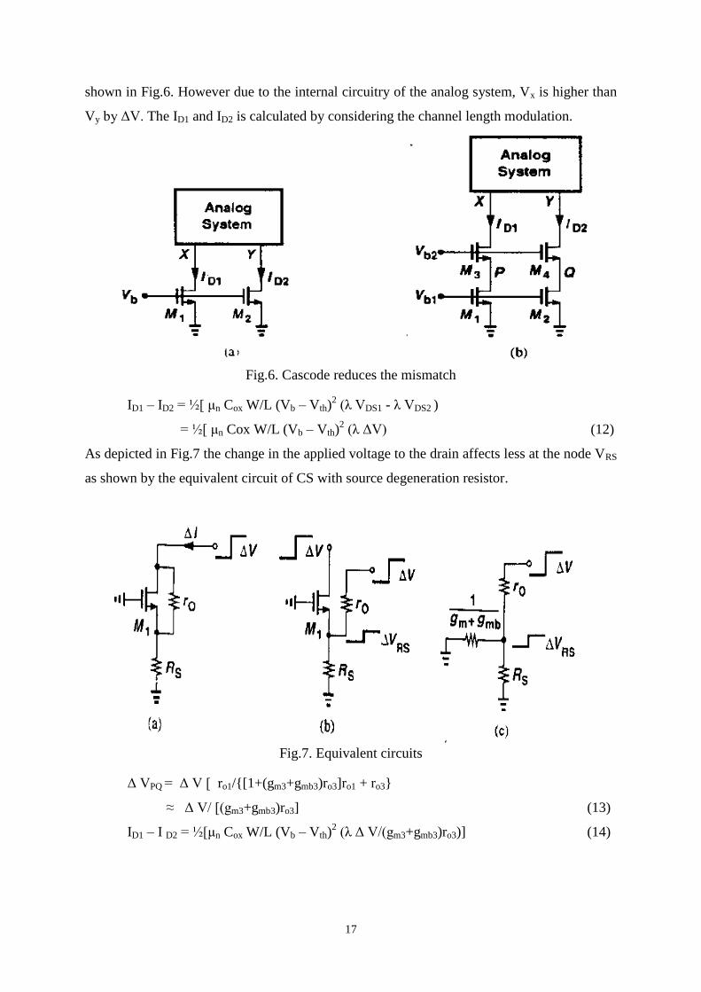
17
shown in Fig.6. However due to the internal circuitry of the analog system, Vx is higher than
Vy by ΔV. The ID1 and ID2 is calculated by considering the channel length modulation.
Fig.6. Cascode reduces the mismatch
ID1 – ID2 = ½[ μn Cox W/L (Vb – Vth)2 (λ VDS1 - λ VDS2 )
= ½[ μn Cox W/L (Vb – Vth)2 (λ ΔV) (12)
As depicted in Fig.7 the change in the applied voltage to the drain affects less at the node VRS
as shown by the equivalent circuit of CS with source degeneration resistor.
Fig.7. Equivalent circuits
Δ VPQ = Δ V [ ro1/{[1+(gm3+gmb3)ro3]ro1 + ro3}
≈ Δ V/ [(gm3+gmb3)ro3] (13)
ID1 – I D2 = ½[μn Cox W/L (Vb – Vth)2 (λ Δ V/(gm3+gmb3)ro3)] (14)
18
In other words, cascading reduces the mismatch between ID1 and I D2 by (gm3+gmb3)
ro3. The cascading reduces the effect of Vx and Vy upon ID1 and ID2 respectively [13]. The
difference ΔV between Vx and Vy translates to a difference ΔVPQ between P and Q equal to
ΔVPQ = ΔV [ro1/ [1+ (gm3+gmb3) ro3] ro1 + ro3]
≈ ΔV/ (gm3+gmb3) ro3 (15)
ID1 - ID2 = ½[μn Cox W/L (Vb – Vth)2 (λ Δ V/ (gm3+gmb3)ro3)] (16)
This proves that the cascading reduces the mismatch between ID1 and ID2 by a factor
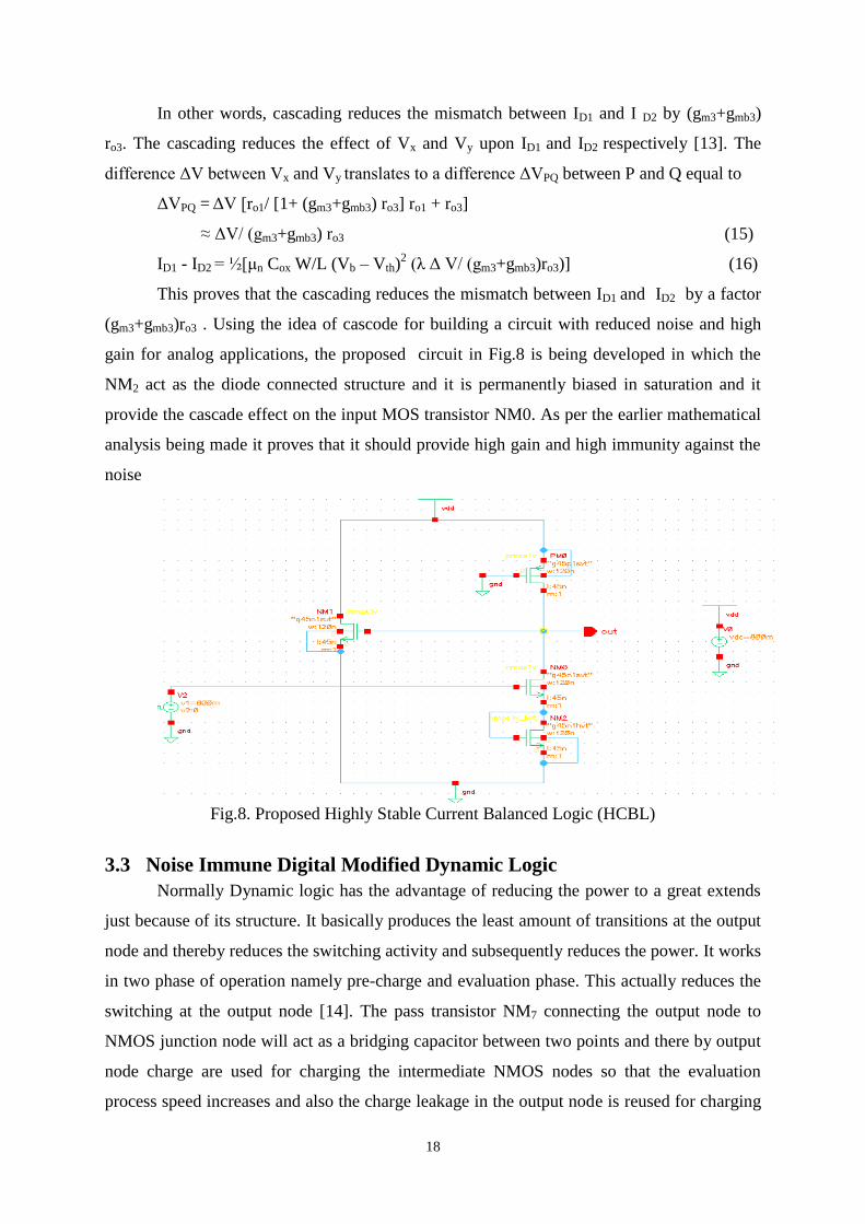
(gm3+gmb3)ro3 . Using the idea of cascode for building a circuit with reduced noise and high
gain for analog applications, the proposed circuit in Fig.8 is being developed in which the
NM2 act as the diode connected structure and it is permanently biased in saturation and it
provide the cascade effect on the input MOS transistor NM0. As per the earlier mathematical
analysis being made it proves that it should provide high gain and high immunity against the
noise
Fig.8. Proposed Highly Stable Current Balanced Logic (HCBL)
3.3 Noise Immune Digital Modified Dynamic Logic
Normally Dynamic logic has the advantage of reducing the power to a great extends
just because of its structure. It basically produces the least amount of transitions at the output
node and thereby reduces the switching activity and subsequently reduces the power. It works
in two phase of operation namely pre-charge and evaluation phase. This actually reduces the
switching at the output node [14]. The pass transistor NM7 connecting the output node to
NMOS junction node will act as a bridging capacitor between two points and there by output
node charge are used for charging the intermediate NMOS nodes so that the evaluation
process speed increases and also the charge leakage in the output node is reused for charging

19
[15-16] the internal nodes, this will reduce the power consumption to a great extent. The
circuit proposed in Fig.9 is used for noise immune low power high speed logic which could
be used for many digital applications.
4. Simulation Results
The proposed circuits are constructed using cadence Analog Design Environment
(ADE) and the various simulations like Transient, AC and DC analysis are made on the
proposed circuits. The parameters considered for simulation are Transistor count, Noise,
Delay, Frequency, Bandwidth and Power The proposed Highly stable Current Balanced
Logic (HCBL) is simulated for a frequency response of about 10 GHz and the simulated
response is shown in Fig .10. The proposed Noise immune Dynamic circuit is constructed as
inverter and 3 input NOR gate.
Fig.9. Noise immune Dynamic circuit
The same circuit is simulated for its functional verification using Spectre with 45nm
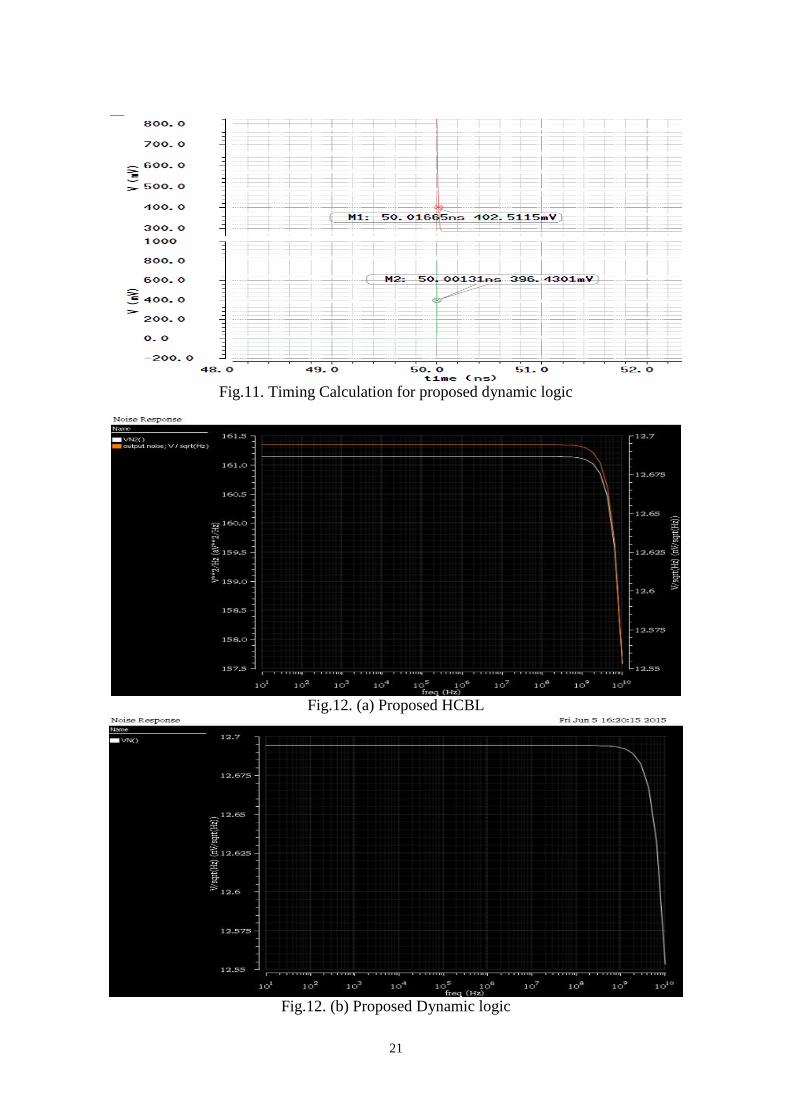
GPDK technology files. The timing calculation (delay) was made between input and output
of the proposed circuit and they have been tabulated in Table: 1. Fig.11 shows the delay
calculation of the proposed circuit in dynamic logic. The power consumption of the circuit
obtained by integrating the current over the whole cycle multiplied with the supply voltage
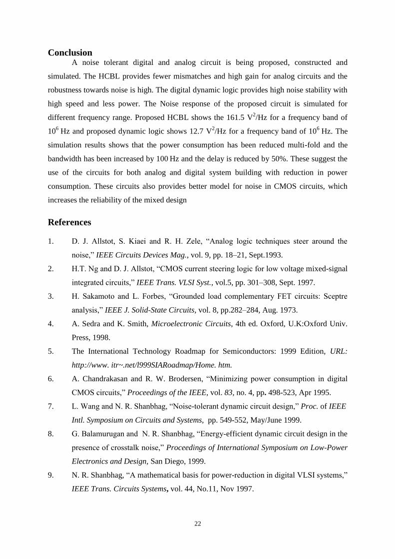
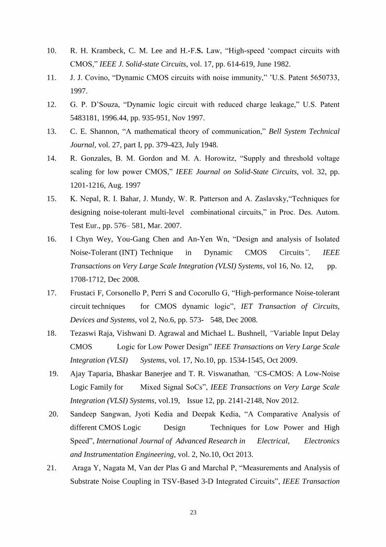
and the same is tabulated in Table: 1. The Noise response of the proposed circuit is simulated
for different frequency range. Proposed HCBL shows the 161.5 V2/Hz for a frequency band
of 106
Hz and proposed dynamic logic shows 12.7 V2/Hz for a frequency band of 10
6 Hz
andthe same has been shown in Fig.12 (a) and (b) respectively. The delay measured with the
proposed circuits is one half compared with the CBL techniques and the bandwidth has been

20
increased by 100 Hz. Also the simulation results tabulated in the Table 1 shows that the
power consumption has been reduced multi-fold for the proposed circuits
Fig.10. (a) Existing CBL Design
Fig.10. (b) Proposed Highly stable Current Balanced Logic
Table. 1 Comparison table of different parameters with the proposed logic
NA- Not Available
Logic
family Type of Logic
No. of
Transistors
Noise
(V2/Hz)
Delay
(ps)
Frequency
(GHz)
Bandwidth
(Hz)
Power
(µW)
CBL NMOS
Inverter 3 NA 16 62.5 10
4 5.512
Proposed
(HCBL)
Logic
NMOS
Inverter 4 161.5 8 125 10
6 0.013
Proposed
Dynamic
Logic
MOS Inverter 4 12.7 7 125 106 0.009
21
Fig.11. Timing Calculation for proposed dynamic logic
Fig.12. (a) Proposed HCBL
Fig.12. (b) Proposed Dynamic logic
22
Conclusion A noise tolerant digital and analog circuit is being proposed, constructed and
simulated. The HCBL provides fewer mismatches and high gain for analog circuits and the
robustness towards noise is high. The digital dynamic logic provides high noise stability with
high speed and less power. The Noise response of the proposed circuit is simulated for
different frequency range. Proposed HCBL shows the 161.5 V2/Hz for a frequency band of
106
Hz and proposed dynamic logic shows 12.7 V2/Hz for a frequency band of 10
6 Hz. The
simulation results shows that the power consumption has been reduced multi-fold and the
bandwidth has been increased by 100 Hz and the delay is reduced by 50%. These suggest the
use of the circuits for both analog and digital system building with reduction in power
consumption. These circuits also provides better model for noise in CMOS circuits, which
increases the reliability of the mixed design
References
1. D. J. Allstot, S. Kiaei and R. H. Zele, “Analog logic techniques steer around the
noise,” IEEE Circuits Devices Mag., vol. 9, pp. 18–21, Sept.1993.
2. H.T. Ng and D. J. Allstot, “CMOS current steering logic for low voltage mixed-signal
integrated circuits,” IEEE Trans. VLSI Syst., vol.5, pp. 301–308, Sept. 1997.
3. H. Sakamoto and L. Forbes, “Grounded load complementary FET circuits: Sceptre
analysis,” IEEE J. Solid-State Circuits, vol. 8, pp.282–284, Aug. 1973.
4. A. Sedra and K. Smith, Microelectronic Circuits, 4th ed. Oxford, U.K:Oxford Univ.
Press, 1998.
5. The International Technology Roadmap for Semiconductors: 1999 Edition, URL:
http://www. itr~.net/l999SIARoadmap/Home. htm.
6. A. Chandrakasan and R. W. Brodersen, “Minimizing power consumption in digital
CMOS circuits,” Proceedings of the IEEE, vol. 83, no. 4, pp. 498-523, Apr 1995.
7. L. Wang and N. R. Shanbhag, “Noise-tolerant dynamic circuit design,” Proc. of IEEE
Intl. Symposium on Circuits and Systems, pp. 549-552, May/June 1999.
8. G. Balamurugan and N. R. Shanbhag, “Energy-efficient dynamic circuit design in the
presence of crosstalk noise,” Proceedings of International Symposium on Low-Power
Electronics and Design, San Diego, 1999.
9. N. R. Shanbhag, “A mathematical basis for power-reduction in digital VLSI systems,”
IEEE Trans. Circuits Systems, vol. 44, No.11, Nov 1997.
23
10. R. H. Krambeck, C. M. Lee and H.-F.S. Law, “High-speed ‘compact circuits with
CMOS,” IEEE J. Solid-state Circuits, vol. 17, pp. 614-619, June 1982.
11. J. J. Covino, “Dynamic CMOS circuits with noise immunity,” ’U.S. Patent 5650733,
1997.
12. G. P. D’Souza, “Dynamic logic circuit with reduced charge leakage,” U.S. Patent
5483181, 1996.44, pp. 935-951, Nov 1997.
13. C. E. Shannon, “A mathematical theory of communication,” Bell System Technical
Journal, vol. 27, part I, pp. 379-423, July 1948.
14. R. Gonzales, B. M. Gordon and M. A. Horowitz, “Supply and threshold voltage
scaling for low power CMOS,” IEEE Journal on Solid-State Circuits, vol. 32, pp.
1201-1216, Aug. 1997
15. K. Nepal, R. I. Bahar, J. Mundy, W. R. Patterson and A. Zaslavsky,“Techniques for
designing noise-tolerant multi-level combinational circuits,” in Proc. Des. Autom.
Test Eur., pp. 576– 581, Mar. 2007.
16. I Chyn Wey, You-Gang Chen and An-Yen Wn, “Design and analysis of Isolated
Noise-Tolerant (INT) Technique in Dynamic CMOS Circuits”, IEEE
Transactions on Very Large Scale Integration (VLSI) Systems, vol 16, No. 12, pp.
1708-1712, Dec 2008.
17. Frustaci F, Corsonello P, Perri S and Cocorullo G, “High-performance Noise-tolerant
circuit techniques for CMOS dynamic logic”, IET Transaction of Circuits,
Devices and Systems, vol 2, No.6, pp. 573- 548, Dec 2008.
18. Tezaswi Raja, Vishwani D. Agrawal and Michael L. Bushnell, “Variable Input Delay
CMOS Logic for Low Power Design” IEEE Transactions on Very Large Scale
Integration (VLSI) Systems, vol. 17, No.10, pp. 1534-1545, Oct 2009.
19. Ajay Taparia, Bhaskar Banerjee and T. R. Viswanathan, “CS-CMOS: A Low-Noise
Logic Family for Mixed Signal SoCs”, IEEE Transactions on Very Large Scale
Integration (VLSI) Systems, vol.19, Issue 12, pp. 2141-2148, Nov 2012.
20. Sandeep Sangwan, Jyoti Kedia and Deepak Kedia, “A Comparative Analysis of
different CMOS Logic Design Techniques for Low Power and High
Speed”, International Journal of Advanced Research in Electrical, Electronics
and Instrumentation Engineering, vol. 2, No.10, Oct 2013.
21. Araga Y, Nagata M, Van der Plas G and Marchal P, “Measurements and Analysis of
Substrate Noise Coupling in TSV-Based 3-D Integrated Circuits”, IEEE Transaction

24
on Components, Packing and Manufacturing Technology, vol. 4, No. 6, pp. 1026-
1037, Apr 2014.
22. Bo Zhao and Huazhong Yang, “Supply-Noise Interactions Among Submodules Inside
a Charge-Pump PLL”, IEEE Transactions on Very Large Scale Integration
(VLSI) Systems, vol. 23, No.4, pp.771-775, Apr 2015.


