
A Millimeter Wave Electro-Optical Transmitter for Radio
over Fiber Systems
Yejun Fu
A thesis
In the Department
Of
Electrical and Computer Engineering
Presented in Partial Fulfillment of the Requirements
For the Degree of Master of Applied Science at
Concordia University
Montréal, Québec, Canada
November 16, 2012
©Yejun Fu 2012

CONCORDIA UNIVERSITY
School of Graduate Studies
This is to certify that the thesis prepared
By: Yejun Fu I.D. 9560335
Entitled: A Millimeter Wave Electro-Optical Modulator for Radio over Fiber
System
and submitted in partial fulfillment of the requirements for the degree of
Master of Applied Science
Complies with the regulations of the University and meets the accepted
standards with respect to originality and quality.
Signed by the final examining committee:
__________ Raut, Rabin ____________ Chair
_____ Sivakumar Narayanswamy ___ Examiner
___ Yousef R. Shaya_________________Examiner
_______________Xiupu zhang________Supervisor
Approved by ____________________________________
Chair of Department or Graduate Program Director
____________________________________
Dean of Faculty
Date_____________________________________
iii
ABSTRACT
Millimeter wave radio over fiber (RoF) system has emerged with competitive
advantages of high bandwidth and low distribution cost to meet the increasing
demanding for high data rate wireless access. In RoF system, optical transmitter
is a key device that is utilized to transmit radio frequency (RF) signal over optical
fiber.
An optical transmitter design involves two important components: Mach Zehnder
Modulators (MZM) and Disturbed Feedback (DFB) Lasers. Unfortunately, the
DFB laser faces aging problem that its slope efficiency and threshold currents
change over time and temperature; the MZMs suffer from bias voltage drift effect,
which leads to an unsteady output power. Power fluctuation reduces gain stability,
which is indeed a problem of RoF system.
The objective of this thesis is to develop an optical transmitter with low cost
circuit design to overcome the above-mentioned issues, by utilizing print circuit
board (PCB) integrated design. The proposed transmitter consists of an MZM, a
DFB laser, a current control circuit, a Thermo Electric Cooler (TEC) control circuit,
and a bias controller, with which the DFB laser produces constant optical power
and the MZM bias controller provides an automatic bias control to obtain a

iv
steady system gain. The designed optical transmitter consists of a stable optical
source and electro-optical modulator (MZM).
Experiments are conducted to assess the performance of the designed optical
transmitter:
(1) The DFB laser with control circuit produces a stable optical output power
(10mW) at wavelength 1550nm. Temperature of the DFB laser has been
investigated which fluctuates no more than 0.2°C.
(2) Flexible bias controller reduces the power penalty for the MZM. It is found that
the MZM’s output power (proportional to system’s gain) biased at quadrature
drifts more than 0.89dB in 30 minutes. On contrary, the output power, with bias
controller, reduces its fluctuation less than 0.03dB. Experiments prove that the
microcontroller is a more advanced technique for MZM’s bias control design.
(3) The RoF system, consisting of designed optical transmitter and a commercial
optical receiver, has been investigated, which provides a 30GHz bandwidth for a
millimeter wave application. Moreover, by maintaining the bias voltage, the bias
controller improves the RoF system’s spurious free dynamic range (SFDR) by
5.35 dB.

v
(4) It is found that the RoF system provides a linear range about 10 dB for
orthogonal frequency division multiplexing (OFDM) ultra-wide band (UWB)
application, regarding the reference standard as -25dB. In addition, transmission
distance impairment for OFDM UWB system is also carried out. We observe that
optimum EVM of this link increases with the extended transmission distance.

vi
ACKNOWLEDGEMENTS
I am sincerely grateful to my advisor, Dr. Xiupu Zhang, for the support and
guidance he showed me throughout my research. I am sure it would have not
been possible without his help.
A special thank goes to Dr. Bouchaib Hraimel for his assistance in project
management and many valuable discussions and worthy suggestions that
facilitated my research. It is a great honor to work with him in the past two years.
I would also like to acknowledge and extend my heartfelt gratitude the faculty,
staff and colleague who shared their personal experience with me. It was a
pleasure to meet and work with these people.
Besides, I would like to thank to my parents and Carol who boosted me morally.
Without your support, encouragement and patient love, I could not have finished
this work.

vii
CONTENT
Chapter 1 Introduction ....................................................................... 1
1.1Background .................................................................................. 1
1.2Millimeter-Wave RoF system ........................................................ 3
1.3Review of schemes for optical transmitter ..................................... 7
1.4Review of key components in optical transmitter .......................... 9
1.5Objective ..................................................................................... 11
1.6PCB and microcontroller design tools ......................................... 13
1.7Thesis outline.............................................................................. 14
Chapter 2 Design of DFB Laser Controller ....................................... 16
2.1 Introduction ................................................................................ 16
2.2 Basics of DFB laser and TEC .................................................... 17
2.3 DFB laser current control circuit ................................................. 20
2.4 TEC control circuit ..................................................................... 24
2.5 Evaluation of DFB laser controller circuit ................................... 27
2.6 Summary ................................................................................... 31

viii
Chapter 3 Design of Mach Zehnder Modulator Controller ................ 32
3.1 Introduction ................................................................................ 32
3.2 Basics of MZM ........................................................................... 34
3.3 Bias controller based on Microchip 16F877A ............................. 40
3.4 MZM bias control circuit evaluation ............................................ 45
3.5 Summary ................................................................................... 51
Chapter 4 Design of Optical Transmitter .......................................... 53
4.1 Introduction ................................................................................ 53
4.2 Structure of optical transmitter ................................................... 55
4.3 Link S-parameters ..................................................................... 57
4.4 Eye diagram .............................................................................. 61
4.5 1dB compression point (P1dB) ..................................................... 64
4.6 Noise figure ............................................................................... 68
4.7 Spurious free dynamic range (SFDR) ........................................ 70
4.8 UWB OFDM transmission in RoF link ........................................ 75
4.9 Impairment of transmission distance for OFDM UWB RoF System
........................................................................................................ 80

ix
4.10 Summary ................................................................................. 83
Chapter 5 Conclusion ...................................................................... 84
5.1 Summary ................................................................................... 84
5.2 Future lines ................................................................................ 86
BIBLIOGRAPHY .............................................................................. 88
A: PCB design flow- OrCAD and PCB editor .................................. 92
B: MPLAB Tool and PIC 16F877A ................................................. 102
C: Code for thermal meter ............................................................. 105
D: Code for bias control ................................................................. 113
E: Design specifications ................................................................. 121

x
LIST OF FIGURES
Figure 1.1 Mobile data and internet traffic growth rate ...................... 1
Figure 1.2 Radio spectrum utilized by a variety of current and next
generation .......................................................................................... 2
Figure 1.3 A basic RoF system ......................................................... 4
Figure 1.4 Dependence of I-L on temperature ................................ 10
Figure 2.1 Structure of a DFB laser ................................................ 17
Figure 2.2 Output spectra of (a) a single longitudinal mode DFB
laser and (b) a multi-longitudinal mode FP laser ............................. 17
Figure 2.3 General structure of a packaged butterfly DFB laser ..... 18
Figure 2.4 The schematic of a TEC unit ......................................... 19
Figure 2.5 The structure of TEC array ............................................. 20
Figure 2.6 The P-I curve of Alcatel 1905 .......................................... 21
Figure 2.7 Schematic the current driver .......................................... 22
Figure 2.8 A H gate TEC control configuration ................................. 24
Figure 2.9 Schematic of temperature controller ............................... 25
Figure 2.10 Temperature configuration ........................................... 26
Figure 2.11 Schematic drawing of laser drive and TEC ................... 27
Figure 2.12 PCB layout of transmitter .............................................. 28

xi
Figure 2.13 DFB laser experimental configuration ........................... 29
Figure 2.14 Temperature vs. rset resistor ........................................ 30
Figure 3.1 Simplified structure of the MZM ...................................... 34
Figure 3.2 Electro-optic modulator transfer function and input/output
(electrical/optical) waveform ........................................................... 37
Figure 3.3 Transfer function and PD current of AM-40 MZM ........... 39
Figure 3.4 Diagram of bias controller ............................................... 40
Figure 3.5 An algorithmic state chart of the bias controller ............... 41
Figure 3.6 Bias shifts Vs. ADC sampling .......................................... 43
Figure 3.7 Schematic design of bias controller................................. 45
Figure 3.8 PCB layout of bias controller ........................................... 46
Figure 3.9 Experimental configuration of bias controller ................... 47
Figure 3.10 A stable MZM output power driven by bias controller .... 48
Figure 3.11 Variable error_10 vs. error_7 ........................................ 49
Figure 3.12 The arrangement of the measuring system .................. 50
Figure 3.13 The MZM output power control by two bias controllers:
CPBC Vs. Microcontroller ................................................................ 51
Figure 4.1 Optical transmitter (a) direct modulation (b) external
modulation ....................................................................................... 53

xii
Figure 4.2 Diagram of optical transmitter……………………………...55
Figure 4.3 The fabricated optical transmitter .................................... 56
Figure 4.4 S parameters testing ....................................................... 57
Figure 4.5 S-parameters at bias voltage of (a) 8.01V and (b) 5.0V .. 58
Figure 4.6 RoF system S-Parameter with PA.................................. 59
Figure 4.7 RoF system S-parameters for 40GHz ............................. 60
Figure 4.8 The experimental setup for eye diagram ........................ 61
Figure 4.9 Measured eye diagram of RoF system at 40Gbps .......... 63
Figure 4.10 input and output characteristics of an amplifier ............. 64
Figure 4.11 P 1dB point at different bias points .................................. 66
Figure 4.12 System gain (a) without bias controller and (b) with bias
controller .......................................................................................... 67
Figure 4.13 Noise figure experimental configuration ........................ 68
Figure 4.14 Illustration of SFDR range ............................................. 70
Figure 4.15 SFDR measurement configuration .............................. 71
Figure 4.16 Output frequency spectrum for two tones and 3rd
intermediations ................................................................................ 72
Figure 4.17 SDFR of optical link with and without bias controller ..... 73

xiii
Figure 4.18 The spectrum allocation for UWB six band groups and
extends from 3.1 to 10.6 GHz ......................................................... 75
Figure 4.19 The 128 subcarriers of a UWB OFDM signal .............. 75
Figure 4.20 OFDM UWB experimental configuration ..................... 76
Figure 4.21 Measurement result by VSA ......................................... 77
Figure 4.22 EVM performances between direct and external
modulations ..................................................................................... 78
Figure 4.23 EVM with and without bias control ................................ 79
Figure 4.24 Experimental setup of OFDM RoF system with different
spools of fiber .................................................................................. 80
Figure 4.25 EVM measured at difference distances ......................... 81

xiv
Table 1.1Comparison of optical transmitter schemes ........................ 8

xv
LIST OF ACRONYMS
Acronyms Definition
ADC Analog to digital conversion
BS Base station
CAGR Compound aggregate growth rate
CS Central station
CW Continue-wave
CPBC Constant average power bias controller
DFB Distribute feedback
DWDM Dense wavelength division multiplexing
DAC Digital to analog conversion
EAM Electrical absorb modulator
EMI Electrical magnetic interference
ESD Electrical statistic discharge
FTTA Fiber to the antenna
FP Fabry-Perot
FBG Fiber Bragg grating
GUI Graphic User Interface
GSM Global system for mobile communication
IM DD Intensive modulation with direct detection
LNA Low noise amplifier

xvi
LED Light emitting diode
LiNbO3 Lithium Niobate
MZM Mach zehnder modulator
NF Noise figure
O/E Optical/electrical
OPAM Operational amplifier
PCB Print circuit board
PIN p-i-n structure
PD Photodiode
PC Polarizer controller
PA Power Amplifier
RF Radio frequency
RoF Radio over fiber
SFDR Spurious free dynamic range
SNR Signal noise ratio
SIP Single in-line package
SA Signal analyzer
SMF Signal mode fiber
TIA Transimpedance amplifier
UMTS Universal mobile telecommunication system

xvii
VSA Vector signal analyzer
VNA Vector network analyzer

1
Chapter 1 Introduction
1.1 Background
Increasing demanding
The data traffic of mobile and portable devices, including text messaging,
multimedia messaging, video call services, and high-speed internet accesses,
are increasing day by day. According to Cisco’s research (see in Figure 1.1),
worldwide demand for mobile and internet traffic has continuously grown from
2009.
Figure 1.1 Mobile data and internet traffic growth rate [1]
The world’s mobile data traffic expands at a compound aggregate growth rate
(CAGR) of 150% between 2008 and 2013 [1]. Thence, the future wireless

2
access network will have to support gigabit data rates. However, current
deployed mobile access network does not offer such high capability.
Problem of conventional wireless access network
The spectrum of wireless access network is shown in Figure 1.2. Multiplicities of
wireless access networks are located from 900 MHz to 5.2 GHz.
Figure 1.2 Radio spectrum utilized by a variety of current and next generation
wireless access networks [2]
The problem of above available wireless access network is that these various
systems are rapidly running out of frequency spectrum. Moreover, sharing at the
same frequency will cause server congestion. Migrating to higher carrier
frequencies (brings more bandwidth) is the only approach to future gigabit data
rate wireless communication [3].
3
1.2 Millimeter-Wave RoF system
Solution :millimeter wave band
Offering broad bandwidth, the millimeter wave is the most promising solution to
achieve high capacity wireless access network. When it comes to the
transmission media for millimeter wave signals, there are three possible options:
air, coaxial cable, and optical fiber. The first option is limited by the high
attenuation (about 15 dB/ km at 60 GHz) [4]; the second one is constrained by
the coaxial cable bandwidth, high cost, and high transmission loss. Avoiding
above problems, the millimeter wave over fiber transmission provides broader
bandwidth, low loss (< 0.5 dB/km), and low cost. Furthermore, millimeter wave
over fiber technique enables to deliver RF signals without interferences [5]. In a
word, millimeter wave RoF technique has been considered as a cost-effective
and reliable solution for the distribution of future wireless access networks.
What is RoF Technology?
RoF is a technology that uses optical fiber to distribute RF signals from a
central site (CS) to groups of separated base stations (BS), which consists of
two different technologies: the radio frequency for wireless communications

4
and optical fiber for wired transmission. One of simple RoF link configurations
called intensity modulation with direct detection (IM-DD) is shown in Figure 1.3
[6].
Figure 1.3 A basic RoF system
RF signals directly modulate the laser diodes in the CS, then the modulated
optical signal is transported over fiber links to a BS, where the RF signal is
recovered by direct detection in the P type-intrinsic-N type (PIN) photodetector.
At last, the amplified signal is radiated by an antenna. Signals can be
transmitted from a BS to the CS, in a similar way [7] [8].
Benefits
RoF systems possess many advantages:
(1) Low attenuation- The attenuation loss of 0.5-inch coaxial cable (RG-214) is
about 500 dB/Km, when it is operated at 5 GHz [9]. However, commercial
5
available Single Mode Fibers (SMFs) made from glass have attenuation loss
below 0.25 dB/km and 0.5 dB/km at 1550 nm and 1300nm wavelength,
respectively [10]. Signals can be transmitted over long distance optical fiber
without much attenuation.
(2)Broad bandwidth- For single mode fiber, the overall available bandwidth is
more than 50THz, except for several high attenuation windows [11]. This
broadband property can be availed by Dense Wavelength Division Multiplexing
(DWDM), which encompasses large number of closely spaced optical signals
over a single fiber. In a 45-channel system spaced at 100GHz, the covered
bandwidth could be 4.5THz [12]. The low-loss window around 1.55um
wavelength is divided into conventional band and long-wavelength band(C band
and L band), which provides a bandwidth of 95nm, corresponding to 11THz.
(3)Immune to Electro Magnetic Interference (EMI) - Fiber optical transmission is
immune to EMI. It is a very attractive property, especially for privacy protection or
secured communication. For instance, the aircraft carrier-USS Ronald Reagan
has built 200 miles optical fiber through a ship-wide maze of plastic tubes for
secured communications [13].
Applications
Several applications of optical communication systems are discussed below:
6
(1)Fiber to the antenna (FTTA) - Connecting optical fiber to the antenna, we can
obtain many advantages like low line loss, immunity to lightning or electric
discharge, and reducing complexity of systems. [8].
(2)CATV- RoF systems can be used to distribute telephone services and
broadcast of multiple video channels over television cables. Such system is also
able to provide a wide range of services, such as telephone, internet and video
broadcasts.
(3)Cellular networks- RoF technology is popular in the mobile communication
networks, especially in a high densely populated area. The RoF system can
provide flexible and effective installation of large numbers of BS in Global System
(GSM) and Universal Mobile Telecommunication system (UMTS) for mobile
communications, for instance during 2000 Sydney Olympics, Allen Telecom
announced a fiber optic-based system. In first day, over 500,000 wireless calls
were made from Olympic Park Venues, which indicates RoF systems are a
successful solution for handling massive wireless accesses [14].
Why 40GHz?
Today, due to the advances in electrical and optical components development,
RoF systems can be designed with high frequency and sufficient signal to noise
ratio (SNR) to transport RF signals for a considerable long distance. However,
7
many limitations will restrict the bandwidth and gain of the RoF system, such as
modulators and power amplifiers. The recent RoF system focuses on 40GHz
transmission, because the available electro optical modulator module only
supports up to 40GHz bandwidth. Furthermore, only few venders can provide
RF broadband amplifiers (40GHz) for millimeter wave applications. In this work,
we adopt a 40GHz MZM and a 40GHz bandwidth power amplifier for the optical
transmitter.
1.3 Review of schemes for optical transmitter
In millimeter wave RoF system, the optical transmitter plays an important role.
The schemes of optical transmitter design can be sorted into two types: direct
modulation and external modulation. Bandwidth and chirp limitation affect the
system performance for the direct modulation. For a high bit rate application, an
external modulation transmitter is often employed, the details of the above two
techniques will be elaborated in Chapter 4.
Two types of external modulator are commonly used: Mach-zehnder Modulator
(MZM) and Electrical Absorb Modulator (EAM). MZMs can provide wide
bandwidth for long distance high-speed communication; EAMs are suitable for

8
medium distance and medium speed application. The details of above three
modulation schemes for an optical transmitter are shown in Table 1.1
Configurations Advantages Disadvantages
Direct modulation
The simplest
scheme
Low cost
Limited modulation
bandwidth of laser (not
suitable for mm-wave
band)
produces chirp
Temperature
dependence
External
modulation(MZM)
Long distance
application
High bandwidth
Expensive
Bias drift effect
Bulky size
External
modulation(EAM)
Highly integrated
with a compacted size
bias voltage drift
free
produces less
chirp
lower extinction
ratio
Table 1.1Comparison of optical transmitter schemes

9
1.4 Review of key components in optical transmitter
Optical sources
A laser source is an essential component in an optical transmitter. The word
LASER stands for Light Amplification by Stimulated Emission of Radiation.
Lasers can be clearly understood by regarding how it amplifies or generates
certain wavelength of light by the stimulated emission of radiation.
Many kinds of optical sources are developed in these years, for example Light
Emitting Diodes (LED), gas lasers, fiber lasers, and semiconductor lasers. One
type of semiconductor lasers named as DFB laser is commonly used as a source
in optical transmitter design. Because the DFB laser possesses compact size,
narrow spectral width and low threshold current.
Drawback of this type of laser is that the wavelength emitted by a DFB laser is
temperature dependent. The laser’s wavelength changes with the increasing of
temperature. For some applications, like dense wavelength division multiplexing
(DWDM) systems with 0.8 wavelength spacing, the laser temperature must be
controlled.
Figure 1.4 illustrates a laser diode with a 3mw output needs drive current about
85mA when it is operated at 10°C. However, if the temperature increases up to

10
90°C, the same output power will need a current of 125mA.The output power of
lasers strongly depends on the temperature.
Figure 1.4 Dependence of I-L on temperature [15]
In a word, the drive current density and output power of lasers will change when
it is subject to an environment with perturbations.
Electro-optical modulators
In 1875, John Kerr discovered certain materials that would change their optical
properties (refractive index) in response to an applied electrical field. The
phenomenon that index changes proportionally to the squared electrical field is
known as the Kerr effect [16]. Although the index changes are tiny, a light wave
propagating through this medium could have a considerable phase change. The
material- Lithium Niobate (LiNbO3) is widely used as a substrate for MZMs.
Distinguishing features of broadband characteristic, low chirp and low driving
voltage (5V) make the MZMs become the dominate modulator in millimeter wave

11
RoF applications. We will elaborate the MZM concerning the structure, transfer
function, and bias drift effect, in Chapter 3.
Main drawbacks of MZMs are high optical insertion loss (4~7dB), large size
(~11cm), sensitivity to the polarization of optical input power and the transfer
function shifting due to the temperature disturbing.
1.5 Objective
Many research works related to RoF systems have been intensively investigated.
The primary objective of this thesis is to build a low cost optical transmitter,
relying on available components, PCB board design, and microcontroller
technique.
Constant optical sources and stable MZM output power play important role in this
transmitter system: a current and temperate control circuit is designed to
overcome the DFB laser’s temperature dependence and aging problem; an
arbitrary bias controller is implemented to compensate the MZM’s bias drift effect.
Based on PCB design and experimental verification, the RoF system parameters
are carried out, which involves the S-parameters, eye diagram, P1dB compression

12
point, SFDR measurement. The results will be compared with different optical
transmitters, and bias controllers.
A practical application of OFDM UWB signal transmitter for the RoF system is
demonstrated, which aims to compare different modulation schemes. Moreover,
the impairment of fiber length to the system performance is investigated. Most
importantly, the optical transmitter is to be built for millimeter wave applications at
an affordable cost.
1.6 General design specification
This optical transmitter design can be used for CATV, antenna remoting,
microwave delay lines and other applications where it is need to transport RF
over long distances without signal degradation. There are two PCB board
designs: The first board carries DFB laser, current control, and temperature
control units, which can generate a tunable optical power range from 9 to 15 dBm.
The temperature control units can maintain the DFB laser from 26C to 32C; the
other board contains logarithmic amplifiers, connectors and voltage regulators,
and a 16F877A micro-controller located on a DIP40 socket. A six pins RJ-11 port
is installed at the back of the board, which connect the 16F877a to a programmer
ICD2. By using software MPLAB, the 16F877A can be reprogramed and
developed for other applications. A LCD 16x2 char LCD are used to interface

13
with microcontroller and show the bias voltage and ADC sample value. This
board is used to compensate the bias drift effect and maintain MZM’s bias
voltage. The bias controller can generate a bias voltage from 1.1 to 8.0V with an
increment of 0.01V.
The external modulated transmitter operates at 1550 nm wavelengths are
available for applications over the 40GHz frequency band and it is a fully
integrated unit that contains both the optics and the control electronics. Only DC
Power supply and the RF input signal are required for operation. A more detailed
table for transmitter’s specification can be found in Appendix E.
1.7 PCB and microcontroller design tools
In this work, the schematic design and PCB layout tools are the OrCAD and PCB
Editor, respectively. The microcontroller-16F877A are developed and programed
by microchip’s MPLAB IDE software.
OrCAD 16.5 is demo version software, which limits the total components placed
in the schematic. The OrCAD Capture can be used for not only schematic design
but also simulation, which can export schematic results (net lists) to the circuit
board layout utility (PCB Editor). The procedures of PCB design, including
schematic design and PCB layout, are introduced in Appendix A.

14
MPLAB is an integrated development environment, which includes several
functions for application development, hardware simulation, and debugging. It
uses both assembly and C programming languages. In Appendix B, the software
MPLAB, the microcontroller 16F877A and programmer ICD2 are introduced.
1.8 Thesis outline
This thesis is composed of five chapters and the rest part of the thesis is
organized as follows:
Chapter 2 introduces a control circuit design for DFB lasers, containing automatic
power control and temperature control. An experiment is set to verify the
performance of this design.
Chapter 3 explicates the working principle of a bias controller for MZMs. The
bias control algorithm is explicated and experiments are conducted to compare it
with another bias control technique.

15
Chapter 4 states the structure of designed optical transmitter, and then we carry
out several experiments to measure the RoF system’s performance. Direct
modulation and external modulation techniques are also compared.
Chapter 5 concludes the thesis and highlights recommendation for future works;
the possible application after this work is addressed as well.

16
Chapter 2 Design of DFB Laser Controller
2.1 Introduction
As previously stated in Chapter 1, the DFB laser is strongly aging and
temperature dependent. Its threshold current increases with the temperature.
Optical sources in the market featuring with power and temperature controller are
quite expensive, and average prices could reach 1500$ or more. Furthermore,
some optical sources may have a quite large size and long warm-up time. For
example, Anritsu MG9541A optical laser source needs one hour to warm up.
The purpose of the control circuit design is to achieve a low cost, small size and
highly stable optical source by using low-cost electronic components. The current
control circuit is used to maintain constant average optical power and the TEC
control circuit is used to regulate the temperature of the laser diode. The DFB
laser with these control circuits can be maintained to generate a constant optical
power to overcome the problem of temperature and aging dependence.
This chapter is organized as follows: Section 2.2 introduces the basic structure of
a DFB laser, the butterfly package and the working principle of TEC. Section 2.3
provides the circuit design of current controller. Section 2.4 shows the detailed
design of TEC control circuit. In section 2.5, an experiment is carried out to
evaluate the performance of the DFB laser using our designed current controller.
In section 2.6, a summary is given.

17
2.2 Basics of DFB laser and TEC
The structure of a DFB laser, which consists of a Bragg grating, P type and N
type semiconductor, is shown in Figure 2.1. The Bragg grating is built on the top
of PN junction. The Bragg grating with a periodic variation index has a similar
function of filter, which allows one longitudinal mode to exist.
Figure 2.1 Structure of a DFB laser [18]
A more intuitive way to understand the function of Bragg grating is shown in
Figure 2.2, which compares two typical output spectra between DFB lasers and
(Fabry-Perot) FP lasers. Unlike the FP laser, the DFB laser has one longitudinal
mode.
Figure 2.2 Output spectra of (a) a single longitudinal mode DFB laser and (b) a multi-longitudinal
mode FP laser [15]

18
The DFB laser diode is usually integrated with PD and TEC, which has a butterfly
package. As we can see in Figure 2.3, the fiber and PD are set at two sides of
the laser diode. The photodiode measures the output power of the laser. The
thermal resistor monitors the temperature of the DFB laser. The above
components are mounted on a metal base. The TEC is stuck at the back of metal
base, which stabilizes the temperature of laser.
Figure 2.3 General structure of a packaged butterfly DFB laser
The TEC is an active cooling system, which is different from a heat sink- a
passive device only used for dissipating heat. The TEC not only lowers the object
temperature but also stabilizes it. TEC is highly reliable and has a compact size,
and it is often used for the temperature controlling in laser systems.
19
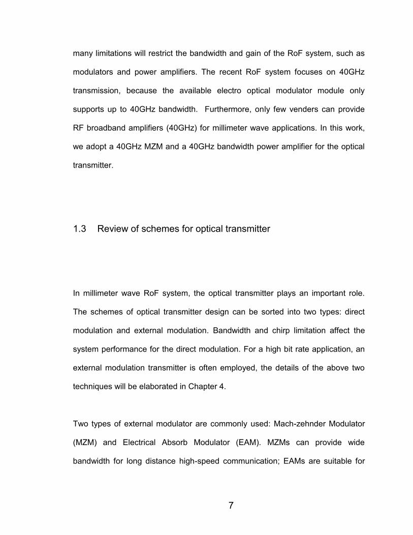
Figure 2.4 presents one TEC unit, which consists of two arrays of P type and N
type semiconductors. Electrical current (see in Figure2.4) circulates through an
N-type semiconductor array, a P-type semiconductor array and inner copper
connectors; meanwhile, heat can be absorbed and transferred from the top side
to the bottom side. Changing the direction of the current, the direction of heat
transfer can be reversed.
Figure 2.4 The schematic of a TEC unit

20
In order to provide a high efficiency of heat dissipation, many of above units are
built and connected together. Figure 2.5 shows a three dimensional structure of
TEC array.
Figure 2.5 The structure of TEC array
2.3 DFB laser current control circuit
The purpose of current control circuit is to provide feedback control to the optical
source and enable the laser to produce a continuous constant power. We use
Alcatel 1905 DFB laser which is integrated with a TEC, PD and thermistor.
As known, a PD is located at the backside of the laser diode to monitor the
optical power. By adding an inverse voltage, the PD produces a current, which is
proportional to the driver current on the laser diode. We measure the P-I curve

21
and PD current of Alcatel 1905 DFB laser. Figure 2.6 presents that the laser
drive current is proportional to the PD current.
Figure 2.6 The P-I curve of Alcatel 1905
From the above figure, it is not difficult to predict that the output power will
fluctuate in a large range, if the drive current is unstable. The current control
circuit must be utilized to ensure the laser to produce a constant power.
We implemented the current driver by iC-WKN, which is an IC that can drive
laser diodes in continue-wave (CW) mode with a maximum 300 mA current. The

22
IC includes integrated circuit protecting against electronic static discharge (ESD)
[19]. The function of iC-WKN is shown in Figure 2.7.
Figure 2.7 Schematic the current driver [19]
A PNP and a NPN transistor are used in the circuit to regulate the laser diode
current in the feedback loop. The optical output power depends on gains of Q1,
Q2 and values of R2. We can derive the relation between pdI and ldI .
2Rbpd III (2.1)
)( 21111 pdRbc IIII (2.2)
221222 pdRbld IIII (2.3)
In equation (2.3), pdI
is proportional to the output power of the laser diode, if the
laser diode power increases, pdI will increases and ldI will decrease accordingly.

23
By changing the value of the resistor R2, the output power of laser diodes can be
adjusted.
From equation (2.3), if R2 value is small, the laser diode will require a high drive
current, which may damage the laser diode. By setting the value of R2, the output
power can be limited. Here we set R2 equal to the sum of two resistors (names
as Rm_fix and Rm_tuning) [19],
MDIMDAVtuningRmfixRm /__ (2.4)
where V(MDA) equals 0.5V, and the absolute maximum PD current I(MD) is
around 1 mA. Therefore, the minimum value of R2 should be 500 which
corresponds to a maximum laser diode driver current, about 350mA. To avoid the
laser diode overload, we add a fixed value resistor about 634 that can limit the
maximum laser diode current of 0.79mA. A trim resistor is added to adjust the
output power.

24
2.4 TEC control circuit
The purpose of TEC controller is to compensate for the thermal effect of laser
diodes. Figure 2.8 represents a typical structure of TEC control circuit which
contains four transistors. As discussed before, the function of TEC is determined
by the direction of current. By letting Q1 and Q4 or Q2 and Q3 open, the bi-
directional current can operate TEC for heating or cooling.
Figure 2.8 A H gate TEC control configuration
A TEC module HY5620 has been implemented which is a subminiature
proportional temperature controller. This device can be used to heat or cool a
DFB laser and maintain the temperature. A thermistor bridge can precisely
measure and regulate the temperature of the TEC. It can deliver up to +/- 2
Amperes of current to a TEC [20].

25
To make TEC control circuit work properly, additional required components are
needed. Figure 2.9 shows the schematic design which contains HY5620, rset,
Rloop, Cloop, R_Crnt_Cool and R_curnt_heat.
Figure 2.9 Schematic of temperature controller
To operate the TEC control circuit, components of capacitor and resistor are
interpreted as follows: Temperature set resistor (rset): rset indicates the
temperature of laser diode when it is stabilized. If resistance of the thermistor in
Alcatel 1905 is equal to rset that indicates the circuit is stabilized.

26
The relation between resistance and temperature is shown in Figure 2.10. For
example, when we set a given temperature to 25C, the resistance of rset is 10kΩ.
Figure 2.10 Temperature configuration [20]
Loop stability (Rloop and Cloop): Rloop and Cloop will determine the time that the
current goes through TEC when it reaches 66% of its final temperature [20]. In
this project, Rloop is set 4.7 M , and Cloop is set 1 F, which indicates the loop
time is around 5 seconds.
Current limit resistors (R_Crnt_Cool and R_curnt_heat): These resistors are used to
protect the TEC and limit the maximum current, when the TEC works in the
cooling or heating cycle. Since the maximum current, used for TEC in Alcatel
DFB laser, is around 1.3 A, R_Crnt_Cool is set to 16.5 K .

27
The working principle of TEC control circuit is: when the temperature of the
Alcatel 1905 laser is higher or lower than the given temperature, the temperature
control will turn on. A maximum cooling current flows into the TEC, or maximum
heating current flows out of the TEC. Once the TEC cools or heats the Alcatel
1905 laser to the given temperature, the current through the TEC will decrease to
maintain the temperature.
2.5 Evaluation of DFB laser controller circuit
As previously stated in Chapter 1, we use OrCAD and PCB editor as the
schematic and layout tools. The schematic drawing contains the control circuits
and Alcatel 1905 laser is rendered in Figure 2.11.
Figure 2.11 Schematic drawing of laser drive and TEC

28
The final layout is shown in Figure 2.12. The DFB laser is located in the middle,
the current and TEC control circuits are placed at left and right side of the board,
respectively.
Figure 2.12 PCB layout of transmitter
To test the stability of the Alcatel 1905 DFB laser, a thermal meter is built with a
microcontroller -PIC16F877A and a temperature sensor DS18B20. The code of
this thermal meter can be found in Appendix C. The DS18B20 digital
thermometer provides 12-bit Celsius temperature measurements. It has an
operating temperature range from -55°C to +125°C. The resolution of the
temperature sensor is 12 bits, corresponding to an increment of 0.0625°C [21].
We set up an experiment to evaluate the performance of the Alcatel 1905 DFB
laser and Figure 2.13 is the experimental setup. The laser current is controlled by

29
a resistor (Rm_tuning). TEC can cool down or heat up the laser diode by the resistor
“rset” (see in Figure 2.11). A power source provides +12V, -12V, and +5V for the
laser and thermal meter. A portable power meter (EXFO) measures the output
power.
Figure 2.13 DFB laser experimental configuration
As mentioned before, the purpose temperature of laser diode is decide by the
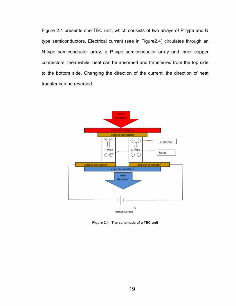
resitance of rset. In Figure 2.14, changing rset from 5 kΩ to 12 kΩ,the laser’s
30
temperature increases at first then becomes stable. It illustrates the small value
of rset will produce a lower stabled temperature as well.
Figure 2.14 Temperature vs. rset resistor
The output power of the Alcatel 1905 laser is maintained at 20 mW. For the
different values of rset, it can be seen the temperature of Alcatel 1905 laser
becomes steady with fluctuation less than 0.2°C, after 20 minutes.

31
2.6 Summary
In this chapter, firstly, we have introduced the basics of the DFB laser and TEC,
which include the physical structure and working principle. Then, we have
explained the detailed design of the current controller and TEC controller. In the
end, we have investigated experimentally the performance of the Alcatel 1905
DFB laser in term of the temperature at a 20 mW optical output power.
Figure 2.14 shows that the temperate of the laser can be maintained. The circuit
has set a current limitation, which can protect the laser diode from accidental
current overload. The laser and control circuits cost less than 400$. The board
only has a size of 3”×6”. Our results indicate that the current and TEC controller
can successfully stabilize the Alcatel 1905 laser. The DFB laser with a steady
optical power is a reliable and perfect light source for optical transmitters.

32
Chapter 3 Design of Mach Zehnder Modulator Controller
3.1 Introduction
Problem: MZM bias drift
The MZM is a preferred modulator for millimeter wave communication, because it
offers a broad bandwidth up to 40GHz. However, MZM has drawbacks of high
optical insertion loss, large size and is polarization sensitive. Furthermore, the
MZM is temperature sensitive. If the MZM is exposed in a fluctuating temperature
environment, its transfer function will drift over time. For this reason, MZM
requires a bias controller to compensate the bias drift.
Solution: Bias controller
Many techniques have been developed to reduce bias drift. We provide an
overview of the present state of MZM bias control technology [22] [23]:
(1) The pilot tone technique: It uses a low frequency signal in a feedback circuit
to maintain the bias voltage. However, this technique has a problem that MZM
with low tone signals may generate strong in-band intermodulation distortion,
resulting in a smaller dynamic range.

33
(2) Microcontroller: This technique is relied on a microcontroller to monitor PD
current that is proportional to MZM output power. Detecting PD current fluctuates;
the microcontroller can correct the bias voltage. Beside the high price, most of
these commercial bias controllers have a big size and only work at maximum,
minimum or quadrature transmission bias points.
(3) Operational Amplifier: unlike a microcontroller, this technique mainly adopts
operational amplifiers in feedback circuit to compensate the bias drift. Limitation
of this technique is that the circuit only can work at one bias point.
Purpose: Low cost, multifunction and arbitrary bias point control
The purpose of our circuit design is to develop an arbitrary bias controller based
on microcontroller technique. We provide a low cost and compact bias control
circuit for an MZM. It relies on an effective method that can operate the MZM at
any bias points by automatically finding the maximum and minimum transmission
bias points. The bias controller can also be easily programmed to provide more
flexible MZM driver for many other applications.
This chapter is organized into five sections. In Section 2, we will introduce the
basics of MZM, such as structure, transfer function and nonlinearity. Section 3 is
devoted to describe the principle of our proposed bias control circuit. In Section 4,

34
experiments are carried out to verify the performance of our bias controller. The
summary is drawn in Section 5.
3.2 Basics of MZM
Structure and transfer function
Lithium Niobate (LiNbO3) is a widely used electro-optical material to modulate the
light in an MZM. Figure 3.1shows a simplified structure of MZM consisting of two
waveguides, two Y junctions and RF/DC electrodes. Assuming that the
modulator is an ideal device with no dispersion, no nonlinearity and no coupling
loss at point A and B; the phase shift at the lower branch is )(t .
A B
Figure 3.1 Simplified structure of the MZM

35
Optical signal is launched into MZM, then it is split into two waveguides at point A.
A voltage V(t) applied at low branch introduces phase change. The two signals
are combined at point B and the output optical field is [22]
VknLiinknLiinout e
Ee
EE 21
222
1
(3.1)
where n is the refractive index of LiNbO3. L1 and L2 are the length of two
waveguides. Equation (3.1) can also be rewritten as
2cos
2cos1
2
1 2 VP
VPP ininout
(3.2)
Obviously, the different phase of two branches plays an important part in
equation (3.2). In practice, two branches often introduce a phase difference.
Equation (3.3) used to describe the relation between the phase shift and the
applied voltage is shown as follows [23]
Ld
VV o
2
(3.3)
where 0 is the original phase difference. This quantity may change due to
fabrication tolerance. is linear electro-optical coefficiency; L and d are the
length and width of the LiNbO3 crystal, respectively; is the wavelength of light
and V is the applied voltage.

36
When the phase shift equals to 90°, a special parameter V is used to specify the
efficiency of electro-optic modulator, which indicates that the bias voltage can
change the MZM transfer function from the maximum to minimum point [23].
L
dV
2
(3.4)
Substituting equation (3.4) into (3.2), the ratio of input and output power can be
simplified as [23]
V
V
P
Po
in
out
2cos2
(3.5)
The equation (3.5) is also known as the MZM power transfer function. Figure 3.2
presents a typical transfer function of an MZM, which shows the relationship
between the input electrical signals and the corresponding output optical signals.
Vb0 is the important bias voltage that will determine the E/O conversion efficiency.
For example, if the input signal is bipolar, the MZM is often biased at quadrature

37
points (Vb0 works at quadrature points), which let the MZM have the best linearity
and the largest swing of the signal voltage.
Figure 3.2 Electro-optic modulator transfer function and input/output (electrical/optical) waveform
[23]
Nonlinearity
However, the transfer function of the MZM is not exactly linear; it is a sine wave,
so the nonlinear part of the MZM transfer function introduces a distortion for RoF
systems. If the applied electrical signal is tVtV m cos)( , the MZM works at
quadrature point, the original phase difference is 90°, the output power can be
expanded as a Bessel series [23]:
...5cos3coscos
2531 txJPtxJPtxJP
PP ininin
inout
(3.5)

38
In equation (3.5), the first term is the average power, the second term is the
linear output, the third and fourth terms are higher order nonlinear harmonics. In
order to avoid higher order distortions, the input signal should be applied with a
lower magnitude voltage. In that case, the high order terms in equation (3.5) can
be neglected. In many applications, quadrature bias point controlling is used to
suppress the nonlinear distortion.
Relation between PD current and transfer function
The MZM transfer function is proportional to its output power which can be
detected by a PD. In this project, we adopt an AVANEX X-cut AM-40 MZM as a
modulator which combines high linearity with low driving voltage and covering the
frequency up to 40 GHz. It also has an Integrated PD with a responsivity of 10-3
[24]. The PD monitors the optical output power of MZM, which is adopted as a
feedback source to control the bias point of the MZM. A simple relation between
the input optical field and the output current can be written as
teteRI 0 (3.6)
where R0 is the responsivity of the PD. If a RF signal is fed to the MZM, an
electrical signal will modulate an optical signal and the optical field at the PD can
be expressed as:
tj
RFcettmvPte
cos10 (3.7)

39
where RF is the RF frequency, c is the optical carrier frequency, 0P is the
optical power, m is the modulation index, v t is the baseband envelop of the
modulated electrical signal. Therefore, the approximate current at PD is
2000 cos1 ttmvPRteteRI RF (3.8)
Measured transfer function of the AM-40 MZM modulator and the PD current is
shown in Figure 3.3.
Figure 3.3 Transfer function and PD current of AM-40 MZM
Obviously, the transfer function is proportional to the PD current (see in Figure
3.3). By using a microcontroller to monitor the PD current, we can adjust the bias
voltage to overcome the MZM’s bias shift effect.
-35
-30
-25
-20
-15
-10
0
0.1
0.2
0.3
0.4
0.5
0 2 4 6 8 10 12
Current of PD(uA)
Transfer function
Bias voltage (V)

40
3.3 Bias controller based on Microchip 16F877A
The block diagram of bias control circuit is shown in Figure 3.4. The MZM (AM-
40) has an integrated PD to monitor its own output power. The OPAM is used as
a transimpedance amplifier (TIA) to convert PD current into voltage. The
microcontroller (16F877A) has three functions: analog to digital conversion
(ADC), Error correction and digital to analog conversion (DAC). DAC0832
module can provide a DC bias voltage to the MZM. The LCD is implemented to
display the bias voltage.
Figure 3.4 Diagram of bias controller
If there are any changes in MZM’s transfer function, it will be reflected on PD
output current and eventually detected by the microcontroller. The error
correction function will decide the value of correction voltage to be applied on the
MZM. However, details of this function will be elaborated later. Once the

41
correction voltage is ready, DAC will send a command to DAC0832 for adjusting
the bias voltage to compensate the bias shift. In Figure 3.5, we show the detailed
working flow of bias controller which can be identified into three phases: (a)
initiation, (b) transfer function sweeping and (c) error checking.
Ideal/Start
(Functions initialization)
LCD screen,ADC,DAC,
Min_Max
DAC
DAC0832
Counter i=0,i++
ADC ADC_out
Min_Max
a
b
Yes
N0
i<255 ?
PD DC bias
AM-40 MZM
Max?
Min?
Calculation/
Arbitrary point
Desired bias
point
ADC
sample
Comparison/
error_int
error_int>10 error_int<10
Yes
Yes
(a)In
itiatio
n(b
)Tra
nsfe
r fun
ctio
n s
we
ep
ing
(c)Error checking
Comparator
Reduce bias
voltage
Increase bias
voltage
Figure 3.5 An algorithmic state chart of the bias controller
(a) Initialization
42
The process begins with initial functions. The circuit contains eight ADC channels,
one DAC convertor and one LCD screen. We have to define the ADC convertor
channel, LCD display pattern, ADC input analog ports, DAC digital output ports
and type of registers.
(b) Transfer function sweeping
Before using the MZM, we have to measure the characteristic transmission
function. The purpose of transfer function sweeping is to utilize microcontroller for
recording the MZM’s transfer function then provide a desired bias voltage to the
MZM.
As shown in Figure 3.5(b), we start with DAC which provides a DC bias voltage
of 1.0V to the MZM. Then the ADC fetches 500 samples of PD voltage and
calculates the average value (see in Figure 3.5). This average sample result
marked as ADC_out is passed to the following function block-comparator (see in
Figure 3.5) to find t he maximum and minimum value. The results are stored in
variable “a” for maximum value, and variable “b” for minimum value (see in
Figure 3.5). The DAC, ADC and Comparator processes will be repeated for 255
times. Because DAC provides an increment of 30mV for each time, the transfer
function sweeping would be able to cover from 1.0V to 8.68V. By this way, the
microcontroller could record the MZM’s transfer function and bias it at arbitrary
bias points.

43
(c) Error checking
After above processes, the MZM should be biased at a desired bias point (see in
Figure 3.5(c)) and the microcontroller will keep running an error checking function
which compares the ADC sample result from PD with desired bias point. The
comparison result is stored in a variable “error_int” which is used to indicate
whether the bias has drifted. For example, in Figure 3.6, the MZM is bias at 5.0V
and the desired bias point is B corresponding to an ADC sample value of 800. If
the transfer function shifts to the right side (red dash line), the error checking
function will sample the PD and the corresponding sample value is 850. After
comparison, the “error_int” equals to -50. By judging this value, DAC can send a
command to DAC0832 and correct the original bias voltage from 5.0V to 5.1V.
Then the microcontroller will run error checking again to ensure the
compensation process is entirely completed.
Figure 3.6 Bias shifts Vs. ADC sampling

44
The purpose of error checking function is keeping the MZM works at it qurdrature
point(point B in Figure 3.6). No matter which side the tranfer function has drifted,
the error check function can adjust the bias voltage to ensure the MZM works at
correct qurdrature points (A or C in Figure 3.6).
The above three steps provide a general understanding for the function of the
bias controller. The complete code can be found in Appendix D.

45
3.4 MZM bias control circuit evaluation
The circuit is designed in OrCAD with the same procedures mentioned in
Appendix A. Figure 3.7 shows the schematic drawing of the bias controller. The
designed circuit contains 16F877A, DAC, LCD, bandpass filter and logarithmic
amplifier (see in Figure 3.7) which can be used for other applications.
16F877A
LCD display
DAC0832
Bandpass filter Logarithmic Amplifier
Signal generator
Programport
Voltage regulators
Reference voltage
Figure 3.7 Schematic design of bias controller

46
The PCB board is fabricated by Centre de Recherche en Electronique
Radiofréquence (CREER). The PCB layout of the bias controller is shown in
Figure 3.8, which has a size of 3.4’’× 3.4’’.
Figure 3.8 PCB layout of bias controller

47
In Figure 3.9, an experimental configuration is conducted to verify the bias
controller. Anritsu MG9541A serves as a light source providing CW laser to the
AM-40 MZM at 1550nm. Since the MZM is polarization sensitive, a polarization
controller (PC) is installed between MG9541A and MZM. An EXFO power meter
measures the output power of MZM.
AM 40 MZMOptical
Powermeter
CW
Bias Controller
Power supply
±12V ±5v
AM 40 MZMOptical
Powermeter
CW
Bias Controller
Power supply
±12V ±5v
MG 9541A Optical source
PC
Figure 3.9 Experimental configuration of bias controller
The transfer function of MZM is Pout/Pin. The input power Pin is a constant power.
The MZM output power (Pout) is proportional to the transfer function. Usually, we

48
measure the optical output power to evaluate the performance of bias controller.
Figure 3.10 shows that our bias controller maintains the MZM output power at
1.05mW for 120 minutes.
Figure 3.10 A stable MZM output power driven by bias controller
We also find that a more steady output power can be achieved by changing the
value of the variable “error_ int” (see in Figure 3.5). The experimental results in
Figure 3.11 show the modified error_int (error_7 in Figure 3.11) can make the

49
power fluctuate less than 0.03dB. On the contrary, the previous code, with the
error_10, has an error shifting around 0.06dB.
Figure 3.11 Variable error_10 vs. error_7
A bias controller design published at World Scientific and Engineering Academy
and Society (WSEAS) is shown in Figure 3.12. Optical power generated by DFB
laser goes into MZM unit and the output power is measured by a power meter
OMM6810-B.
A constant average power bias controller (CPBC) circuit monitors the TIA
(represent the PD power) and generates the desired bias voltage to the MZM. A

50
data collection unit (DAQ) is used to gather information regarding the optical
output power, PD current and Bias voltage.
Figure 3.12 The arrangement of the measuring system [25]
The CPBC circuit is mainly built with operational amplifiers, a technique we
mentioned previously. The TIA output voltage is fed into CPBC that will compare
this voltage with a reference voltage and generate a differential voltage to
compensate the bias drift.
Performance of CPBC is compared with our bias controller and the result is
presented in Figure 3.13. The experiment result of CPBC is marked as OPAM
(red circle); our bias controller is marked as microcontroller (blue diamond). The
CPBC can sustain the output power with fluctuation less than 0.35dB. Our bias
controller can maintain the optical power steadily around -0.5dBm with a

51
fluctuation no more than 0.1dB. Figure 3.13 indicates the microcontroller
technique can provide a more accurate bias control method.
Figure 3.13 The MZM output power control by two bias controllers: CPBC Vs. Microcontroller
3.5 Summary
This chapter has presented a comprehensive overview concept of bias control
circuit. Firstly, we introduced and compared different techniques used for bias
controller. Then, we described the basics of MZM including its structure, transfer
function and nonlinearity. We explained the main function of bias controller. At

52
the end, an experiment was set up to evaluate the control circuit. The result
obtained from experiment shows that the bias controller is feasible to maintain
the output power of MZM. We found the microcontroller is a more advanced
technique for bias controlling. We provide a low cost and compact bias control
circuit for MZM. The whole board costs less than 100$ with a compact size of
3.4’’×3.4’’. Furthermore, the bias controller can be programmed for other
applications.
53
Chapter 4 Design of Optical Transmitter
4.1 Introduction
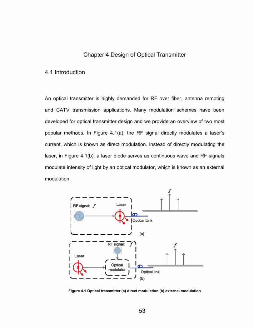
An optical transmitter is highly demanded for RF over fiber, antenna remoting
and CATV transmission applications. Many modulation schemes have been
developed for optical transmitter design and we provide an overview of two most
popular methods. In Figure 4.1(a), the RF signal directly modulates a laser’s
current, which is known as direct modulation. Instead of directly modulating the
laser, in Figure 4.1(b), a laser diode serves as continuous wave and RF signals
modulate intensity of light by an optical modulator, which is known as an external
modulation.
Figure 4.1 Optical transmitter (a) direct modulation (b) external modulation
54
The laser diode in direct modulation technique has two functions: a laser source
and a modulator. Although the direction modulation is the simplest scheme, it is
hard to be applied for high frequency, like millimeter wave systems. Limitations
of bandwidth and laser nonlinearity make it impossible to modulate millimeter
wave signals directly on a laser. Thus, at high frequencies, such as above
10GHz, external modulation is a preferable solution.
In this chapter, we utilize an external modulation scheme for our optical
transmitter. The low noise, narrow line width Alcatel DFB laser is adopted as a
CW light source. The broadband optical modulator AM-40 MZM is employed to
provide the modulation bandwidth up to 40 GHz. Combing with the previously
stated MZM bias controller and DFB laser control circuit, the designed optical
transmitter can be utilized for millimeter wave band applications.
This chapter is organized as follows: Section 2 introduces the structure of
designed optical transmitter. From Section 3 to Section 7, we conduct
experiments to evaluate the transmitter’s performance including S-parameter,
1dB compression point, noise figure, SFDR and eye diagram. Section 8 and 9
present UWB OFDM signal transmission over a RoF system. At the end, we
draw out the summary, including a table of the system’s parameter.

55
4.2 Structure of optical transmitter
Figure 4.2 shows the structure of our optical transmitter. The Alcatel 1905 DFB
laser is served as 10mW CW laser at 1550nm. Meanwhile, the current and
temperature driver maintain the optical output power. The AM-40 MZM
modulates RF signals into optical form that is transmitted over optical fiber. As
mentioned before, the bias drift of MZM limits the system performance. A precise
bias controller is used to compensate bias drift, which enables the transmitter
has good output power stability. Since the AM-40 MZM has a high insertion loss
of 6 dB, a commercial power amplifier (ZVA +213) is used to increase the system
gain.
Alcatel 1905
Current
controlTemp
control
Fiber
AM- 40 MZM
CW LDMonitor PDMonitor
PD
Bias controller
ADCDAC
DCOptical
outputRF
Power amplifier(PA)
Figure 4.2 Diagram of optical transmitter

56
Figure 4.3 shows the final PCB board after soldering. The MZM is not mounded
on the PCB board, because we have to share this MZM for other experiments.
The most common operating bias points of MZMs are negative slope quadrature,
positive slope quadrature, minimum transmission (also called null) and maximum
transmission point [26]. In this work, experiments are conducted with the MZM
operated at positive slope quadrature point corresponding to a bias voltage
around 1.8V.
MZM
Figure 4.3 The fabricated optical transmitter
The optical transmitter is well fabricated. Several experiments will be carried out
to demonstrate that this product can work as we expected. The following section
will show the experiment details and results.
57
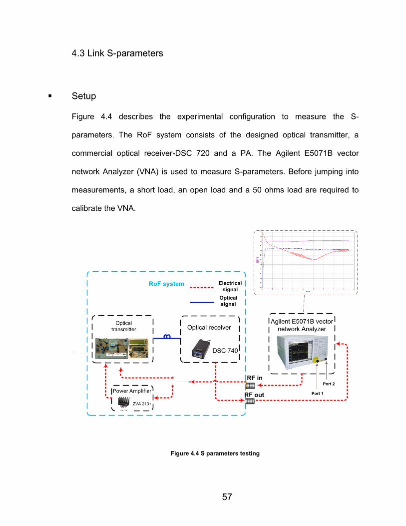
4.3 Link S-parameters
Setup
Figure 4.4 describes the experimental configuration to measure the S-
parameters. The RoF system consists of the designed optical transmitter, a
commercial optical receiver-DSC 720 and a PA. The Agilent E5071B vector
network Analyzer (VNA) is used to measure S-parameters. Before jumping into
measurements, a short load, an open load and a 50 ohms load are required to
calibrate the VNA.
Agilent E5071B vector
network Analyzer
RoF system Electrical
signal
Optical
signal
Optical receiverOptical
transmitter
DSC 740
Power Amplifier
ZVA 213+
RF in
RF out Port 1
Port 2
Figure 4.4 S parameters testing

58
From VNA’s port 1, RF signals from 300 KHz to 8.5GHz are sent into incident
port of DUT (the RoF system). The transmitted signals are fed back to VNA’s port
2. Thus, the VNA can analyze the system’s return loss and transmission
coefficient.
Result(without PA)
We record S-parameters at two bias voltages in Figure 4.5. Experiment result
indicates that two bias points of 8.01V (maximum transmission point) and 5.0V
(minimum transmission point) can largely change the system’s gain.
Figure 4.5 S-parameters at bias voltage of (a) 8.01V and (b) 5.0V
In Figure 4.5 (a), the S11 is below -10.533dB (see maker m1) and the S22 is less
than -8.756dB (see marker m2). The S11 and S22 have few changes when the
MZM is biased at 5.0V, in Figure 4.5 (b). However, the systems gain (S21)

59
decreases dramatically, from -45 dB at maximum transmission point (bias
voltage of 8.01V) to -75 dB at minimum transmission point (bias voltage of 5.0V).
Result (with PA)
The system gain (S21) is low (-45 dB) even MZM is biased at the maximum
transmission point, so a PA (ZVA +213) is added into RoF system to provide a
gain of 27dB. The measured s-parameters are shown as follows:
Figure 4.6 RoF system S-Parameter with PA
In Figure 4.6, the S11 parameter is below -10dB after 418MHz (see m1) and S22
is no more than -8.286dB (see m2). From 404MHz to 8.5GHz, the system
produce a stable gain curve around is -18 dB (see m3 and m4).

60
Result of 40GHz measurement
The Agilent E5071B (VNA) only covers a maximum bandwidth up to 8.5 GHz. To
evaluate the system performance at millimeter-wave frequencies, we measure
the S-parameter at CREER by using VNA Anritsu 37269B which can test S-
parameters up to 40GHz. A 100GHz U2t photodetector is adopted to replace the
DSC740 (optical receiver), since the DSC740 only has a 3-dB detection
bandwidth of 26GHz. Figure 4.7 shows the S-parameters of the RoF system.
Figure 4.7 RoF system S-parameters for 40GHz
The return loss S11 is below -10dB, except for frequencies around 30GHz, which

61
corresponds to a worse performance of -8.65 dB. The S22 is less than -9.9 dB,
which indicates the output port of U2t photodetector is well matched. The 3dB cut
off frequency of our RoF system is around 30.40GHz.
4.4 Eye diagram
Setup
In this experiment, we evaluate RoF system by analyzing the “eye diagram”
which is often used to assess the performance of communication systems.
Figure 4.8 shows the experiment setup.
Agilent infiniium 86100C
RF out
MP1800A
Signal quality Analyzer RoF system Electrical
signal
Optical
signal
Optical receiverOptical
transmitter
DSC
10H-39
PARF in
SHF
810
pseudo-random
bits
Figure 4.8 The experimental setup for eye diagram

62
MP1800A is a pulse pattern generator with four channels of parallel data output
lines. It can produce PRBS pattern up to 231-1 bits. A 40GHz wideband PA-
SHF810 is implemented to deliver a sufficient gain for RF signals. The PA
cascaded with an attenuate mainly provides a gain of 10 dB. Optical receiver-
DSC10H-39 offers a detection bandwidth of 45GHz. Agilent infiniium 86100C
Oscilloscope is used to analyze the eye diagram.
Result
The pulse generator provides pseudo-random bits for the RoF system, with a 1
Vp-p input signal at a bit rate of 40Gbps. For each displayed bit period, there will
be Highs, Lows, and Up and Down transitions (see in Figure 4.9). With a properly
trigger, the measured results are repeatedly displayed which looks like an eye
(see in Figure 4.9).

63
Figure 4.9 Measured eye diagram of RoF system at 40Gbps

64
Figure 4.9 shows the output voltage swing (V p-p) has reached 50.914 mV and the
Q factor (S/N) is 9.16.
4.5 1dB compression point (P1dB)
The P1dB is a commonly used figure of merit to shows the gain relationship
between output power and input power for RF amplifiers. A typical RF amplifier
(nonlinear device) response is shown in Figure 4.10.
Figure 4.10 input and output characteristics of an amplifier
Figure 4.10 plots the input, output power data, and gain of an amplifier, with
linear and nonlinear curves. The measured output power (Pout data) is plotted

65
against the ideal linear response (Pout linear), where these two lines diverged by
1 dB is noted as the P1dB point (see point “A” in Figure 4.10). However, by
comparing measured gain curve with the ideal linear gain response, we also can
obtain P1dB point (see point “B” in Figure 4.10). It is also known as a swept-power
gain compression method, which not only can be used for amplifier but also our
RoF system.
We use the same experimental setup, which is shown in Figure 4.4. Sweeping
the RF input power from -30dBm to -5dBm, the VNA measures the system’s gain
to obtain the P1dB point.

66
Result
To evaluate system’s gain at different transmission points, we measure the RoF
system’s gain with fourteen different MZM bias voltages, from 1.1V to 8.1V. A
table containing six P 1 dB points and corresponded bias voltages is shown in
Figure 4.11.
Figure 4.11 P 1dB point at different bias points

67
For a transmitter, usually P1dB is referred to output power. In our circumstance,
the system gain changes with different bias voltages, therefore, the P1dB is
defined as input power. In Figure 4.11, we measured several P 1dB values, and
the average value of RoF system’s P 1dB is -9.18 dB, approximately.
Stability of system’s gain
As mentioned before, the system’s gain is affected by the bias voltage. The bias
drifting leads to an unstable gain curve. In Chapter 3, we only evaluate the bias
controller by measuring the output power of the MZM; however, we can also
investigate the bias controller by testing the system’s gain as a function of time.
We set the RoF system at fixed bias voltage and measure the system’s gain
several times, in Figure 4.12.
Figure 4.12 System gain (a) without bias controller and (b) with bias controller

68
Figure 4.13 compares the system gain with and without bias controller. In Figure
4.13(a), we start to measure the S21 at 17:37(time), after 10 minutes the S21
curve drops down about 0.7dB. At 18:40, it almost decline around 1dB.
However, in Figure 4.13(b), the gain curve is stable with a shifting no more than
0.2 dB, in one hour. The bias controller has a good ability to maintain a steady
system gain curve.
4.6 Noise figure
We measure the RoF system’s noise figure (NF) which is a parameter of the
degradation in signal to noise ratio between input and output. A low NF means a
little noise is added by the system. Figure 4.13 shows the experimental setup.
Agilent Spectrum
Analyzer
RoF system Electrical
signal
Optical
signal
Optical receiverOptical
transmitter
DSC
10H-39
RF in
RF out
50 Ohms
Load
Figure 4.13 Noise figure experimental configuration

69
A 50 Ohms load is mounted on the RF input port, the spectrum analyzer (SA)
measures the power spectral density of the thermal noise. The measured noise
floor is around -141.54dBm/Hz.
The input noise power can be calculated by fTKP b =- 174.288dBm where,
where f is the resolution bandwidth, T is room temperature, and
Kb is Boltzmann's constant. The RoF system gain is -18 dB. The Noise figure can
be calculated by
dB
N
NG
N
N
S
SNF
i
o
i
o
o
i 748.14)288.17454.141(18 (4.2)
where iS and iN represent the signal and noise levels available at the input to
the RoF system, oS and oN represent the signal and noise levels available at the
output.
70
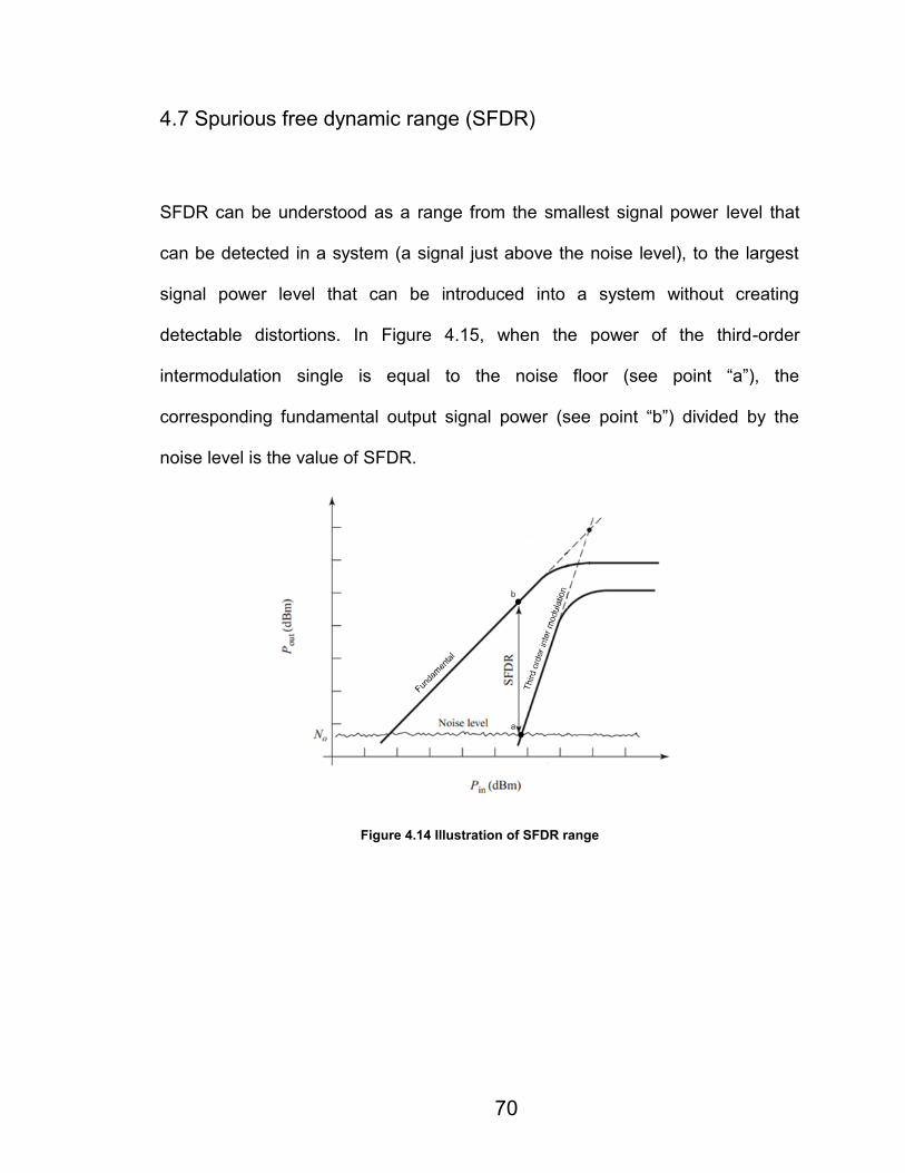
4.7 Spurious free dynamic range (SFDR)
SFDR can be understood as a range from the smallest signal power level that
can be detected in a system (a signal just above the noise level), to the largest
signal power level that can be introduced into a system without creating
detectable distortions. In Figure 4.15, when the power of the third-order
intermodulation single is equal to the noise floor (see point “a”), the
corresponding fundamental output signal power (see point “b”) divided by the
noise level is the value of SFDR.
Figure 4.14 Illustration of SFDR range

71
Setup
Figure 4.15 presents an experimental setup to analyze the SFDR. Two signal
generators produce two equal amplitude signals but differ in frequency by 4.0
MHz from each other (f1:4.960GHz and f2:4.964GHz). A microwave hybrid
combines two tones and feeds them to the RoF system. Two tones and
intermodulation signals are sent into the SA where power level of two tones and
intermodulation signals can be observed.
Figure 4.15 SFDR measurement configuration

72
Since the RoF system is not linear, the intermodulation distortion occurs when
two tones (f1:4.960GHz and f2:4.964GHz) are injected into the system. The
intermodulation output signals occur at (2f1-f2: 4.956GHz), and at (2f2-f1:
4.968GHz), which is close to f1 and f2 (see in Figure 4.16). Third order
intermodulation signals will increase 3 dB for every increased 1 dB the input
signals.
Figure 4.16 Output frequency spectrum for two tones and 3rd
intermediations
Result
We measure two input signals power level (f1 and f2) and four output signals
power level (f1, f2, 2f1-f2, and 2f2-f1) then plot them in Figure 4.17. The above

73
signals are recorded for two times: with bias controller (Marked as “with_B_”) and
without bias controller (marked as “without_B_”).
Figure 4.17 SDFR of optical link with and without bias controller
Figure 4.17 illustrates two tones and the third order intermodulation signals’
output power vs. input power. If we linearly extend portions of these plots (see in
Figure 4.17), they would eventually intersect at the Third Order Intercept point
(IP3). If we draw a noise floor of the system (-171.54dBm/Hz in this system), and
linearly extend above plots, which will give us two intersect points (“a” and “b”,
see in Figure 4.17). According to the definition, the SFDR is the power of point “c”
or “d” divided by noise floor. Since the power is measured in dB, we can subtract

74
noise floor from output power “c” or “d” to calculate SFDR value. Learning from
Figure 4.17, the RoF system has a SFDR of 104.2 dB with a bias controller, and
a SFDR of 97.07 dB without bias controller. The bias controller can suppress the
nonlinearity and provide a larger SFDR by maintaining the MZM at the
quadrature bias point.

75
4.8 UWB OFDM transmission in RoF link
An application of transmitting UWB OFDM signal over RoF system is carried out.
The EVM measurements are used to evaluate the system’s performance, which
can identify sources of signal degradation, such as carrier leakage, phase noise ,
I-Q imbalance and non-linearity. The OFDM is a popular modulation solution for
short distances and high data rate applications. The UWB OFDM signal consists
of 128 subcarriers which can be data carriers, pilot carriers, guard carriers, or null
carriers. Each carrier has a 4.125 MHz bandwidth, and the total six groups
occupy 528 MHz bandwidth. Figure 4.18 and Figure 4.19 illustrate UWB band
groups and band #1 structure, respectively.
Figure 4.18 The spectrum allocation for UWB six band groups and extends from 3.1 to 10.6 GHz [27]
Figure 4.19 The 128 subcarriers of a UWB OFDM signal [27]

76
Setup
The experimental configuration is shown in Figure 4.20. The AWG 7122B with
RFXpress generates group 1 carrier 2 UWB OFDM signal which has a center
frequency of 3.96GHz and bandwidth of 528MHz. The spectrum analyzer
(Advantest u3772) measures the channel power of UWB signals. The input
channel power is -13dBm with a data rate of 480Mbps and a package size of
1024. Combining a low noise power amplifier (LNA) with an attenuator, we can
tune the input power from -13dBm to 8dBm. At the receiver, a LNA is also
implemented to improve the system’s gain. The Agilent Infiniium DSO81204B
oscilloscope tests the EVM performance of received OFDM UWB signals.
Figure 4.20 OFDM UWB experimental configuration

77
Result
The oscilloscope contains vector signal analyzer software (VSA)-89600 which
provides flexible tools for demodulating and analyzing UWB OFDM signals.
Figure 4.21 shows a screen shot of measured result, including constellate
diagram, spectrum of channel signals, and channel’s composite error summary.
Figure 4.21 Measurement result by VSA
Figure 4.21provides lot of system information. In this experiment, we mainly use
EVM value to investigate system’s performance. Figure 4.22 is the measurement
result. Tuning the input channel power from -13dB to 8dB, we measure the EVM
as a function of input power.
In Figure 4.22, when input power is low, the EVM reduces with an increasing

78
input power until it reaches to the optimum point “a” (see in Figure 4.22) that
corresponds to the lowest EVM of -27dB. If we continue to increase the input
power, the EVM will start to increase, because the OFDM signal starts being
affected by the system’s nonlinearity.
Figure 4.22 EVM performances between direct and external modulations
We also compare EVM of our RoF system with an optical transceiver that mainly
uses direct modulation technology. In Figure 4.22, the RoF system has a good
linearity of the input power from -7 dBm to 7 dBm (referred to EVM of -25 dB).
Our RoF system (blue diamond line) has a larger linear range and lower optimum

79
point than the optical transceiver (red circle line). The external modulation is a
more advanced technique than direct modulation.
Stability of EVM
Similar to Section 5, we also investigate the performance of bias controller by
observing the EVM with or without the bias controller, respectively. Figure 4.23
shows the measured EVM in 200 minutes.
.
Figure 4.23 EVM with and without bias control
In Figure 4.23, the system with bias controller (blue square line) has a smoother
EVM curve, except the point a, b, and c which has a fluctuation of 0.2 dB.
However, the system EVM performance without bias controller is out of our

80
expectation, which has a fluctuation no more than 0.5dB. Here, we may be able
to conclude that the EVM performance is not sensitive to the bias voltage drift.
4.9 Impairment of transmission distance for OFDM UWB RoF System
Setup
Based on the experiment in Section 4.8, we attempt to increase the transmission
distance to investigate the impairment of transmission distance for an OFDM
UWB RoF system, regarding the EVM performance. Figure 4.24 illustrates the
experimental configuration which uses almost the same setup in Section 4.8, but
only changes the transmission distances.
Figure 4.24 Experimental setup of OFDM RoF system with different spools of fiber

81
Result
Figure 4.25 shows the measured EVM at different transmission distances from
1km to 30km, and the optimum EVM points are marked with a black dot.
Figure 4.25 EVM measured at difference distances
In this experiment, we combine one 1, 2, 4, 8, and 20Km fiber spool to make a
transmission distance that ranges from 1Km to 30Km. Adding extra adaptors
and patch cables will introduce loss, for example a 3Km fiber may has a higher

82
loss than 4 Km fiber, and that is the reason why the transmission distance of
27Km brings a lower optimum point than a 30Km transmission distance(see in
Figure 4.24).
The EVM optimum point increases from -27.06 dB to –24.21 dB, when we extend
the transmission distances. From Figure 4.25, we also find that when the input
RF power is low, the loss introduced by different distance limits the EVM
performance. However, for a high input power, the intermodulation effect
dominates the system, and signal to noise ratio (SNR) remains the same value,
which lead to the same EVM.

83
4.10 Summary
In this chapter, we compared two different modulation techniques for optical
transmitter and introduced the structure of our optical transmitter. Then, several
experiments were carried out to evaluate the RoF system’s performance. In
Section 8, we compared EVM performance of two different modulation systems.
In Section 9, we investigated the impairment of transmission distance for OFDM
UWB RoF system.

84
Chapter 5 Conclusion
5.1 Summary
This Master thesis has provided a study of electro-optical modulator integrated
optical transmitter design for RoF millimeter wave system, by using PCB circuit
design and microcontroller technique. In this work, functions of fabricated board
have been explicated and verified. Many issues about the optical transmitter are
presented.
Firstly, the thermal effect and power control have been shown as the main
problem for the DFB laser. It is pivotal for a DFB to produce a steady output
power in optical transmitter design. Experiments show that our laser control
circuit can maintain the DFB laser output power at 20mW with a temperature
fluctuation less than 0.2°C. The designed laser source features as low cost,
stable, and short warm up time (less than 20 minutes).
Secondly, bias drift effects on the MZM has been reduced by using the
demonstrated algorithm. By revising the code, the bias controller can operate the
bias voltage more precisely. It has been proved that the microcontroller is a more
advanced technique for bias controlling which processes low cost, flexible, and

85
multifunction. We have demonstrated that the bias controller steadily maintains
the MZM’s output power with a fluctuation no more than 0.1dB.
Thirdly, employing the designed optical transmitter and a commercial optical
receiver, we have carried out several experiments to evaluate the RoF system
that can provide a 3dB bandwidth of 30.4GHz. We have shown the feasibility of a
40Gbps data link over the RoF system, which has a good Q factor of 9.16. From
the experimental results, the bias controller has a good performance to maintain
system’s gain and improve the SFDR around 5.35 dB. In a nutshell, the designed
optical transmitter is viable for millimeter wave band applications with a low cost
no more than 500$ (cost of the MZM are not included).
Furthermore, we have compared two modulation schemes for the OFDM UWB
signal transmitted over the RoF system. From the results, we conclude that the
external modulation system has a larger linear range and better EVM
performance than direct modulation system. It is also found that EVM
performance is not sensitive to the bias voltage drift.
At the end, we have investigated impact of fiber length on the EVM performance
for OFDM UWB RoF system. Expanding the optical length from 1 to 30 km, the
optimum EVM point grows exponentially 2.5dB (referred to input power). We
conclude that the main reason of signal degradation in this system is MZM’s
nonlinearities and chromatic delay introduced by optical fiber.

86
5.2 Future lines
We recommend that further research be undertaken in the following areas:
smaller size, component relocation
Firstly, the microchip 16F877A and display module take up lots of space on the
PCB board. To reduce the board size, future design could choose these
components with a compacted package, such as surface mount chips. Moreover,
the board is designed with two layers and plenty of components can be placed at
the backside. Secondly, the power dissipation was not concerned when the parts
were placed. During the measurement, the temperature of the PCB board, close
to voltage regulators, is considerably high. Therefore, the location of some
components, such as the power regulators may not appropriate. We suggest to
replace voltage regulators with single in-line packages (SIP).
More functions for lasers and more accurate bias voltage for MZMs
Press keys, a screen, and a temperature sensor can be added to set and display
the DFB laser’s parameters (drive current, optical output power, and laser’s
temperature). Moreover, this board can offer sophisticated functions, for instance
laser diode overload protection, high temperature warning, and shutdown
precaution process. In addition, changing components, such as a more advanced

87
microcontroller, 12 bit ADC/DAC and more accurate reference voltage regulators,
the bias controller can provide a more precise operation with an accuracy of 1mV.
Application: low noise tunable optical source
Adding an ultra-narrow Fiber Bragg Grating (FBG) and a circulator to the DFB
laser, a noise suppression laser source can be achieved. A low pilot tone is being
sent to the laser, then goes into circulator and FBG that will reflects this signal
back to the microcontroller. Comparing the reflected signal with the original pilot
tone, the microcontroller uses PMW function (integrated in microcontroller) to
control a TEC plate (attached under the FBG), which can shift the FBG’s
transmission peak, thermally. The above processes can be understood as a
wavelength locker. If the DFB laser’s carrier frequency shifts, the microcontroller
and the TEC will act as a tunable filter to correspondingly alternate FBG’s center
wavelength. Therefore, the fluctuations that fall out of the peak frequency are
rejected [28].
88
BIBLIOGRAPHY
[1] Cisco, "Cisco Visual Networking Index: Forecast and Methodology, 2008–
2013," Cisco, 2009.
[2] C. H.Lee, "Microwave Photonics", CRC Press, 2007.
[3] B.Razavi, "Gadgets gab at 60GHz," Spectrum, IEEE, vol. 45, no. 2, pp. 46-
58, 2008.
[4] Smulders, "Characterisation of propagation in 60 GHz radio channels,"
Electronics & Communication Engineering Journal, vol. 9, no. 2, pp. 73-80,
1997.
[5] X. Z. a. J. Y. Zhenbo Xu, "Frequency upconversion of multiple RF signals
using optical carrier suppression for radio over fiber downlinks," Optics
Express, vol. 15, no. 10, pp. 16737-16747, 2007.
[6] K. K. Masataka Nakazawa, in High Spectral Density Optical Communication
Technologies, Springer, 2010, p. 337.
[7] S. K. Hamed AI-Raweshidy, Radio over Fiber Technologies, Norwood:
ARTECH HOUSE.INC, 2002.
[8] A. Ng'oma, "Radio-over-Fibre Technology for Boradband Wireless
Communication Systems," 2005.
[9] K. D.Wake, "A Novel Swithched Fiber Distributeed Antenna System," in
European Confernce on Optical Communications, 2004.
[10] C. DeCusatis, Handbook of Fiber Optic Data Communication, New York:

89
2007.
[11] L. D.K.Mynbaev, Fiber Optic Communications Technology, New Jersey:
Prentice Hall, 2001.
[12] EMcore, "Dense Wavelength-division Multiplexing," EMcore, 20 11 2012.
[Online]. Available: http://www.fiber-
optics.info/fiber_optic_glossary/dense_wavelength-
division_multiplexing_dwdm.
[13] D. McGray, "wired," wired.com, 2003. [Online]. Available:
http://www.wired.com/wired/archive/11.09/navy.html.
[14] K. G. Stavros A.Kotsopoulos, "Handbook of Research on Heterogeneous
Next Generation Networking," Idea Group Inc, 2008, p. 584.
[15] K. T. Ajoy Ghatak, "An Introduction to fiber otpics," New York, Cambridge
University Press, 1998, p. 233.
[16] P. Weinberger, "John Kerr and his Effects Found in 1877 and 1878,"
Philosophical Magazine Letters , 2008.
[17] E. Säckinger, "Broadband Circuits For Optical Fiber Communication," in
Optical fiber, JOHN WILEY & SONS INC, 2005, p. 11.
[18] G. Agrawal, in Fiber-Optic Communication Systems, NY, John Weily & Sons,
Inc, 2002, p. 101.
[19] i. Haus, "15V CW LASER DIODE DRIVER iC WKN datasheet," [Online].
Available: http://www.ichaus.de/upload/pdf/Wkn_b1es.pdf.
[20] H. Microsystems, "HY5650 TEC Controller Operating Manual," hytek

90
microsystems, [Online]. Available: esl.eng.ohio-
state.edu/~rstheory/iip/hy5650_manual.pdf.
[21] M. I. DELEVOR, "Programmable Resolution 1-Wire Digital Thermometer,"
maxim integrated, 2008. [Online]. Available:
http://www.maximintegrated.com/datasheet/index.mvp/id/2812.
[22] H. AI-Rweshidy, Radio over Fiber Technologies for mobile Communications
Networks, Artech House, 2002.
[23] R. Hui, Fiber optic measurement techniques, Academic Press, 2009.
[24] oclaro, "20/40G Intensity modulators for analog applications," Oclaro, Inc. ,
[Online]. Available: http://dev.oclaro.com/product_pages/Powerlog_AM-
40.php.
[25] J. ŠVARNÝ, "Limited Applicability of the Constant Optical Power Controller
to the Integrated Intensity Electro-Optic Modulator," in 10th WSEAS
International Conference on ELECTRONICS, HARDWARE, WIRELESS and
OPTICAL COMMUNICATIONS, 2011.
[26] J. Yao, "A Tutorial on Microwave Photonics," IEEE Photomics Society
Newsletter, 2012.
[27] Wikipedia, "UWB," [Online]. Available: http://en.wikipedia.org/wiki/Ultra-
wideband.
[28] Y. P. C. L. M.-J. P. Jean-Francois Chiche, "Ultra-Narrow Bragg Grating for
Active Semiconductor Laser Linewidth Reduction through Electrical
Feedback," in Fibre Grating Sensors, Quebec City, 2007.

91
[29] K. Brunham, Writer, Introduction to orcad. [Performance]. Embedded
soulutions, 2002.
[30] M. T. Inc., "Quick Guide to Microchip Development Tools,"2008.
[31] M. T. Inc, "28/40/44-Pin Enhanced Flash Microcontrollers," 2003.

92
APPENDIX
A: PCB design flow- OrCAD and PCB editor
OrCAD
In this section, we briefly introduce the design flow of schematic design by using
Or-CAD and Figure A.1 illustrates its graphic user interface (GUI) operation
windows.
Figure A.1 Windows capture

93
For the schematic design, we can follow the flow in Figure A.2.
Figure A.2 Capture design flow [29]
At first, we need to select the components (ic, capacitors, resistors, etc.) from the
library. For each component, a symbol must be created, which is a physical view
of the component that contains all the pins of the component and properties.
Each component used in schematic design must have an associated footprint
used for PCB Layout. The capture provides most of the libraries. However, a few
special symbols might need to be created, according to datasheet, as an
additional symbol library for a new design. Cadence provides a software named
PAD design that can let you draw special component footprint. Meanwhile,
Footprint Maker could also yield the standard diameters of most common

94
components. For example, in this design, HY5620 TEC driver is a special model.
We have to make a footprint according to its datasheet.
Second, procedure can be ended by placing to schematic board and then
connecting all components by wires. All the properties of parts must be set, for
example values, PCB part names, symbols etc. Components must be placed in
the schematic and connected by wires. Beside, for some designs, extra symbols
may also need to be placed, for instance texts, test points, power and ground
symbols.
At the end, the design rules check (DRC) should be executed to ensure above
processes that are meet all constraints which defined by users.
A DRC checking must be examined the schematic. If it is passed, a net list file
will be generated, which can be used in the PCB editor layout.
PCB editor
Figure A.3 displays a blank board file opened in the PCB Editor. There are six
working areas in this design window. Various tools are placed in toolbars and
many aspects of component characteristics can be controlled, like trace
highlights, etching edits, DRC checks, etc. Any characteristics can be regulated

95
in these toolbars, including visible or hidden line and component locations. The
command window presents information and allows users to type commands. The
worldview window provides an overall view of the location and the size of the
design windows corresponds to the actual PCB. The status bar shows the
coordinates of the crosshairs. The P and A field indicate the coordinates. Here
are several important procedures in PCB layout work.
Figure A.3 PCB editor windows
Creating board: After importing the net list, a border outline needs to be created.
It could be done by opening the PCB Editor then going to Setup and selecting
Design Parameter in Figure Under the Display menu, the grids can be set up,
which is an important parameter. At the Design tab, the size of the work place
and the drawing extents can be set suitably. The whole units for this project are

96
mils and inches. Because, the PCB board is fabricated at the University of
Montreal and it has to meet the specific requirements for the machine.
Figure A.4 PCB editor design parameter configuration
A board can be added by clicking the Add button then choosing Rectangle, in
Figure A.4. In the Options, by selecting Board Geometry as the Class and
Outline as the subclass, a board outline of dimensions 6000 Mils by 3400 Mils
can be established. PCB Editor also provides a command window. Writing “x 0 0”
means a point is set at location (0, 0); then writing again “x 34000 6000” sets the
upper right coordinates of the rectangle. A Board outline can be created by these
two commands.

97
For some applications, multilayer may be needed. Figure A.5 shows a window to
set up multilayers. The window shows the default two layers PCB and inserted
two more FR4 and two more copper layers(GND, VCC), which is a four layer
PCB.
Figure A.5 Multilayer configuration
Setting up constraint conditions and VIAs: Before placing and routing circuit,
a set of router specifications need be set down. Several important design rule
constraints need be defined.
Defining Trace Width and Spacing Rules: Line width choice can be made
based on several key factors. The first is the thickness of PCB board. Depending
on the capability of PCB board parameters, a minimum line width is
recommended on datasheet. The second factor is the current limitation. For a

98
certain value of current, a line width can be calculated out by equations [29]. The
third factor is the frequency of signal, which decides the width of lines. In this
project, all signals are low frequency, so the line impedance is not concerned.
The line space is important when the signal is high voltage and big current. In
this project, since a sufficient area can be used to route, it is not a key factor and
it was set as 15mils. Rogers RO4000® high frequency circuit materials are
selected as PCB board. The RO4350B has a dielectric constant of 3.48 and
thickness of 30mils. In this design, the signal line width is 15mils. For high speed
signals and highly integrated circuits, to limit the circuit size, the line width and
space could be a crucial factor. What’s more, these parameters also depend on
the fabrication capability. All the PCB circuit is made by Polytechnique de
Montreal, and the minimum line width is 6mils, the minimum line space is 10mils.
Assigning cutting marks, Alignment donut, and vias: Since Polytechnique de
Montreal has its own requirements for all design. Four right angle etching line
with a length of 200mils and width of 20mils are set at the corner of circuit. These
four marks are cutting marks. In a word, the inside of four right angle area is the
real size of circuit. During the manufacture, vias are also important. The holes,
which connecting top layer and bottom layer have a relatively small size. In order
to insure the accuracy, three alignment holes with a shape of donuts are
mounted at the outside of layout. These donuts have a 66mils inner and 120mils
outer diameter. The vias, in this design, are set as a 31mils hole with a 60 mils
pad.

99
Placing components and routing: After finishing above procedures, parts can
be placed. Choosing Place button at manual from the menu bar can place parts.
The Placement dialog box is shown in Figure A. 6.
Figure A.6 Manually placing components
One of components can be selected in the sub tab-Component by refdes box.
Once it was been selected, the part is automatically transferred to the design
window. When the entire components are placed, the board is ready to route.
Clicking one, trace will be highlighted. Selecting Add Connect button and clicking
the trace will show as an etching line with real line width. In some conditions, a
via is need to connect traces between two different lays.

100
DRC checking and generating gerber and drill files: At this stage, all the
components, lines are placed and routed. A procedure named as design rule
checker (DRC) should be executed. A message indicates whether there are
errors. Then PCB Editor generates a design file used to fabricate the final board.
The most common file applied in manufacturing system is Gerber file. The design
file that is required by Polytechnique is Gerber RS-274X. Figure A.7 shows a
dialog box which can configure the parameter of the gerber file. The Gerber file
should have a precision of 2.4, which can be defined at Format option. The
integer places are two and the decimal place is four.
Figure A.7 Artwork control form1

101
Choose Yejunfu-S1B and Yejunfu-S1T layer, in Figure A.8. S1T indicates this is
top layer, the other S1B is bottom layer. Undefined line with option is eight mils.
This decides the size of extra texts. In Figure A.8, the bottom of the board has a
line with the name of the circuits, the designer, the types and width of board. This
line is made by etching line with a line width of eight mils.
Figure A.8 Artwork control form2
By finishing above procedures, the final gerber file of top and bottom layout can
be generated. A drill file in form of dxf contains all the via information, like
alignment donuts, cutting marks and diameters of vias, is also need by
Polytechnique de Montreal.
In brief, the PCB design follows five processes:

102
Start with schematic design with OrCAD
Generate netlists and transfer to PCB layout
Set up board size, constraint management, line and via size
Place components and route the board
Generate Gerber files and drill files
B: MPLAB Tool and PIC 16F877A
MPLAB is an integrated development software which can be used to program the
microchip. Figure B.1 displays the working windows of MPLAB. It is a Microchips
Integrated Development Environment and includes several components for
application development, hardware simulation and debugging. It uses both
Assembly and C programming languages with MPLAB.
Figure B.1 Work windows of MPLAB

103
Figure B.2 shows the programmer MPLAB® ICD 2 used in this project. It is an
all-in-one programmer, a low cost, real-time debugger and programmer for PIC®
MCUs. “Using Microchip Technology's proprietary In-Circuit Debug functions,
programs can be downloaded, executed in real time and examined in detail with
the debugging functions of MPLAB. Setting watch variables and breakpoints from
symbolic labels in C or assembly source code, the program can single steps
through C source lines or into assembly code. MPLAB ICD 2 can also be used as
a development programmer for supported MCUs [30].”
Figure B.2 Programmer ICD 2 [30]
By using a USB cable, the ICD 2 connects the design user's PC and the target
board. It allows users to look into the target board's microcontroller, view
variables and registers at breakpoints with MPLAB watch windows.

104
Microcontroller PIC 16F877A
A microcontroller (MCU) is a small scale computer on a single integrated circuit
containing a processor core, memory and programmable input output peripherals,
which can be used for embedded applications [42]. In this project, microchip
PIC16F877A is adopted, which is CMOS FLASH-based 8-bit microcontroller
pack with 40 pins. Figure G.3 shows the pin diagram of 16F877A. In order to test
and debug the final board, a DDIP package is selected. PIC16F877A features
256 bytes of EEPROM data memory, self-programming, an ICD, 8 channels of
10-bit Analog-to-Digital (A/D) converter, 2 additional timers, 2
capture/compare/PWM functions, a synchronous serial port, which can be
configured as either 3-wire Serial Peripheral Interface (SPI™) or the 2-wire Inter-
Integrated Circuit (I²C™) bus, and a Universal Asynchronous Receiver
Transmitter (USART) [31]. The PIC61F877A provides 8 channels (A/D) which
makes it ideal for more advanced level A/D applications.
Figure B.3 Pin diagram of 16F877A

105
C: Code for thermal meter
#include "pic.h"
__CONFIG(0x2F0A); #define uchar unsigned char #define uint unsigned int #define DQ RD5 #define DQ_HIGH() TRISD5=1 #define DQ_LOW() TRISD5=0;DQ=0 #define RS RD0 #define RW RD1 #define E RD2 #define CS RD3 #define WR RD4 //#define ILE RD5 //#define XFER RD6 uchar pacmanopen[] = 0x0E,0x07,0x03,0x01,0x03,0x07,0x0E,0x00,'\n'; uchar pacmanshut[] = 0x00,0x0F,0x1F,0x01,0x1F,0x0F,0x00,0x00,'\n'; //Display Config. #define MAX_DISPLAY_CHAR 19 //LCD Registers addresses (PORT B) #define LCD_CMD_WR 0x00 #define LCD_DATA_WR 0x01 #define LCD_BUSY_RD 0x02 #define LCD_DATA_RD 0x03 //LCD Commands #define LCD_CLS 0x01 //clean the screen, cursor to 0 position, #define LCD_HOME 0x02 //cusor to 0 position #define LCD_SETMODE 0x04 #define LCD_SETVISIBLE 0x08 #define LCD_SHIFT 0x10 #define LCD_SETFUNCTION 0x38// 0x20 8 bit one line*******0x38 8 bit two lines #define LCD_SETCGADDR 0x40 #define LCD_SETDDADDR 0x80 #define E_PIN_MASK 0x04 #define Newline 0xC0 void disp(uchar num1,uchar num2,uchar num3,uchar num4); void disp1(uchar num1,uchar num2,uchar num3,uchar num4); void lcd_init(); void adc_init(); void lcd_wait(); void clearscreen(); void wrcmd(uchar cmdcode); void wrdata(uchar data);

106
void pause(uint num); void eat(); void Delay_mS(uint D); void clearscreen (); void adc_start() ; void InitialiseADC (unsigned char ADC_Channel); void adc_enable(unsigned char channel) ; void adc_read(); void readout(uchar data); uint temper; uchar a1,a2,a3,a4; void delayus(uint,uchar); void delayus1(uchar); void delay(uint); void write_byte(uchar date); uchar read_byte(); void get_tem(); ////------------------------------------------------------// uint i; uint advalf0; uint adval0; uint adval1; uchar text[] = '0',',','0','0','0'; uchar text1[] = 'T','e',' ','0','0','.','0','0',' ','C'; void main() uint i,lednum,lednum1; float dacout; uchar a0,a1,a2,a3,a4; lcd_init(); adc_init(); TRISC=0x00; // PORTC=0x00; while(1) lcd_init(); wrcmd(Newline); get_tem(); /************** adc_enable ******************/ void adc_enable(unsigned char channel) ADCON0 = (channel << 3) + 0x81; // ADC on, Fosc/32 /************** adc_read ********************/ void adc_read() ADGO = 1; // start A/D-conversion

107
while(ADGO) // wait continue; /************** adc_start ******************/ void adc_start() uint adres0; uint adres1; float advalf1; float advalf2; adc_enable(0); // chanel 0 adc_read(); // begin adres0 = ADRESH; // AD-Wert save adres0 = adres0 << 8; adres0 = adres0 | ADRESL; advalf1=(adres0/1023.0)*255.0;//==2.3843 adval0=advalf1*1; return; /**********************************************************/ void adc_init() TRISA=0x07;//set the port 1 2 3 as input
TRISB=0x00; PORTA=0;
ADCON1=0x8e; //set up the up and low value Delay_mS(10); void pause(uint num) // Utility routine to pause for // a period of time. while(num--) /*do nothing */ /**************DRIVER**********************************************************/ void lcd_init() // Initialise the LCD Display. TRISB = PORTB = 0x00; TRISD=0x00; wrcmd(LCD_SETFUNCTION); // 8-bit mode - 2 line - 5x7 font. wrcmd(LCD_SETVISIBLE+0x04); // Display no cursor - no blink. wrcmd(LCD_SETMODE+0x02); //wrcgchr(pacmanshut, 8); // Automatic Increment - No Display shift. //wrcgchr(pacmanopen, 0);

108
wrcmd(LCD_SETDDADDR); // Address DDRAM with 0 offset 80h. void clearscreen () wrcmd(LCD_CLS); wrcmd(LCD_SETDDADDR+0x00); void wrcmd(uchar cmdcode) PORTB=cmdcode; RS=0;
RW=0;
Delay_mS(1); E=1;
Delay_mS(1); E=0;
return; void wrdata(uchar data) PORTB=data; RS=1;
RW=0;
Delay_mS(1); E=1;
Delay_mS(1); E=0;
return; void Delay_mS(uint D) unsigned int i,j; for(i=0;i<D;i++) for(j=0;j<1000;j++); void disp(uchar num1,uchar num2,uchar num3,uchar num4) uchar *textptr = text; uint i;

109
text[0] = num1; text[2] = num2; text[3] = num3; text[4] = num4; for(i=0;i<5;i++) // Write the String. wrdata(*textptr++); pause(10); void disp1(uchar num1,uchar num2,uchar num3,uchar num4) uchar *textptr1 = text1; uint i; text1[3] = num1; text1[4] = num2; text1[6] = num3; text1[7] = num4; for(i=0;i<10;i++) // Write the String. wrdata(*textptr1++); pause(10); //************DAC FUNCTION**************************************// void readout(uchar data) PORTC=data; CS=1;CS=0;
WR=1;WR=0;
Delay_mS(1); WR=1;CS=1;
return; void reset() uchar st=1; DQ_HIGH();
delayus1(0); //2uS while(st) DQ_LOW(); delayus1(250); //500uS DQ_HIGH();
delayus1(19);//40uS if(DQ==1) st=1; else

110
st=0; delayus1(250); //500uS void write_byte(uchar date) uchar i,temp; DQ_HIGH();
delayus1(0); for(i=8;i>0;i--) temp=date&0x01; //01010101 DQ_LOW(); delayus1(2); //7~15.8uS if(temp==1) DQ_HIGH(); else
DQ_LOW() ;
delayus1(25); //25~51.8us
DQ_HIGH();
date=date>>1; //00101010
NOP();NOP();NOP();
NOP();NOP();
uchar read_byte()
uchar i,date;
static bit j;
for(i=8;i>0;i--)
date=date>>1;
DQ_HIGH();
delayus1(0); //2.2us
DQ_LOW();

111
delayus1(1); //3.8uS
DQ_HIGH();
delayus1(0); //5.8uS
j=DQ;
if(j==1)
date=date|0x80;//1000 0000
else date=date|0x00; delayus1(22); //17~ 37uS //18~56 19~ 60uS //45US (22/20) return (date); void get_tem() uchar tem1,tem2,num; float aaa; reset(); write_byte(0xCC);// write_byte(0x44);// //write_byte(0x4E);/ delay(2000); disp1(a1,a2,a3,a4); reset(); write_byte(0xCC); write_byte(0xBE); tem1=read_byte(); tem2=read_byte(); aaa=(tem2*256+tem1)*6.25; temper=(int)aaa; a1=temper/1000+48; a2=temper%1000/100+48; a3=temper%100/10+48; a4=temper%10+48; delay(2000); delay(2000); delay(2000); void delayus(uint x, uchar y) uint i; uchar j; for(i=x;i>0;i--); for(j=y;j>0;j--); void delayus1(uchar x) uint i;

112
for(i=x;i>0;i--); void delay(uint x) uint a,b; for(a=x;a>0;a--) for(b=110;b>0;b--);

113
D: Code for bias control
#include "pic.h" #include "stdlib.h" __CONFIG(0x2F0A); const float bb[]=3.72,3.73,3.74 ,3.75 ,3.76 ,3.77 ,3.78 ,3.79 ,3.8 ,3.81 ,3.82 ,3.83 ,3.84 ,3.85 ,3.86 ,3.87 ,3.88,3.89,3.9, 3.91 ,3.92 ,3.93 ,3.94 ,3.95 ,3.96 ,3.97 ,3.98 ,3.99 ,4.00 ,4.01 ,4.02 ,4.03 ,4.04 ,4.05 ,4.06 ,4.07 ,4.08 ,4.09 ,4.1, 4.11 ,4.12 ,4.13 ,4.14 ,4.15 ,4.16 ,4.17; const float cc[]=3.72,3.73,3.74 ,3.75 ,3.76 ,3.77 ,3.78 ,3.79 ,3.8 ,3.81 ,3.82 ,3.83 ,3.84 ,3.85 ,3.86 ,3.87 ,3.88,3.89,3.9, 3.91 ,3.92 ,3.93 ,3.94 ,3.95 ,3.96 ,3.97 ,3.98 ,3.99 ,4.00 ,4.01 ,4.02 ,4.03 ,4.04 ,4.05 ,4.06 ,4.07 ,4.08 ,4.09 ,4.1, 4.11 ,4.12 ,4.13 ,4.14 ,4.15 ,4.16 ,4.17; unsigned char texta[] = 'D',' ','0','0','0','0'; #define uchar unsigned char #define uint unsigned int #define RS RD0 #define RW RD1 #define E RD2 #define CS RD3 #define WR RD4 #define ILE RD5 #define XFER RD6 uchar pacmanopen[] = 0x0E,0x07,0x03,0x01,0x03,0x07,0x0E,0x00,'\n'; uchar pacmanshut[] = 0x00,0x0F,0x1F,0x01,0x1F,0x0F,0x00,0x00,'\n'; //Display Config. #define MAX_DISPLAY_CHAR 19 //LCD Registers addresses (PORT B) #define LCD_CMD_WR 0x00 #define LCD_DATA_WR 0x01 #define LCD_BUSY_RD 0x02 #define LCD_DATA_RD 0x03 //LCD Commands #define LCD_CLS 0x01 //clean the screen, cursor to 0 position, #define LCD_HOME 0x02 //cusor to 0 position #define LCD_SETMODE 0x04 #define LCD_SETVISIBLE 0x08 #define LCD_SHIFT 0x10 #define LCD_SETFUNCTION 0x38// 0x20 8 bit one line*******0x38 8 bit two lines #define LCD_SETCGADDR 0x40 #define LCD_SETDDADDR 0x80 #define E_PIN_MASK 0x04 void disp(uint lcdnum);

114
void lcd_init(); void adc_init(); void lcd_wait(); void clearscreen(); void wrcmd(uchar cmdcode); void wrdata(uchar data); void pause(uint num); void eat(); void Delay_mS(uint D); void clearscreen (); void adc_start() ; void InitialiseADC (unsigned char ADC_Channel); void adc_enable(unsigned char channel) ; void adc_read(); void readout(uchar data); void disptext(uchar text); void disp1(uint lcdnum); void check_error(); void max_min(); void Delay_m(uint D); uint i; uint advalf0; uint adval0; uint adval1; uint vbias; uint max; uint min; uint bias_a; uint bias_b; float error; signed int error_int; uint aim_point; uint flag; uchar text[] = '0','.','0','0','0'; uchar ok[]='o','k',' ','!'; void main() uint i,lednum,lednum1; float dacout,num1,num2; // uchar a0,a1,a2,a3,a4; lcd_init(); adc_init(); TRISC=0x00; PORTC=0x00; Delay_mS(1000);

115
//max_min(); //vbias=(bias_b+bias_a)/2; //vbias=160; readout(vbias); adc_start(); disp(vbias); //Delay_mS(7123); adc_init(); adc_start(); clearscreen (); check_error(); while(1) if(error_int>7) vbias=vbias+1; readout(vbias); Delay_mS(2000); check_error(); else if(error_int<-10) vbias=vbias-1; readout(vbias); Delay_mS(2000); check_error(); else(abs(error_int)<7); check_error(); /************** error check ******************/ void check_error() float dacout,num1,num2; if(flag<1) adc_start(); Delay_mS(1000); aim_point=adval0; disp(aim_point); num1=adval0; disp(num1); error=(aim_point-num1); error_int=error; wrcmd(0xC0); //disp1(abs(error_int)); Delay_mS(2000); wrcmd(LCD_CLS); flag++;

116
adc_start(); Delay_mS(1000); num2=aim_point; disp(num2); num1=adval0; disp(num1); error=(num2-num1); error_int=error; wrcmd(0xC0); disp1(abs(error_int)); Delay_mS(2000); wrcmd(LCD_CLS); /************** adc_enable ******************/ void adc_enable(unsigned char channel) ADCON0 = (channel << 3) + 0x81; // ADC on, Fosc/32 /************** adc_read ********************/ void adc_read() ADGO = 1; // start A/D-conversion while(ADGO) // wait continue; /************** adc_start ******************/ void adc_start() uint adres0; uint adres1; float advalf1; float advalf2; adc_enable(0); // chanel 0 adc_read(); // beginn adres0 = ADRESH; // AD-Wert save adres0 = adres0 << 8; adres0 = adres0 | ADRESL; advalf1=(adres0/1023.0)*3.5;//==2.3843 adval0=advalf1*1000; //adval0=advalf1/255; return; /***************************adc_int*******************************/ void adc_init() TRISA=0x09;//set the port 1 2 3 as input
TRISB=0x00;

117
PORTA=0;
ADCON1=0x85; //set up the up and low vavle Delay_mS(10); /**************************pause**********************************************/ void pause(uint num) // Utility routine to pause for // a period of time. while(num--) /*do nothing */ /************DRIVER******************/ void lcd_init() // Initialise the LCD Display. TRISB = PORTB = 0x00; TRISD=0x00; wrcmd(LCD_SETFUNCTION); // 8-bit mode - 2 line - 5x7 font. wrcmd(LCD_SETVISIBLE+0x04); // Display no cursor - no blink. wrcmd(LCD_SETMODE+0x02); //wrcgchr(pacmanshut, 8); // Automatic Increment - No Display shift. //wrcgchr(pacmanopen, 0); wrcmd(LCD_SETDDADDR); // Address DDRAM with 0 offset 80h. void clearscreen () wrcmd(LCD_CLS); wrcmd(LCD_SETDDADDR+0x00); void wrcmd(uchar cmdcode) PORTB=cmdcode; RS=0;
RW=0;
Delay_mS(1); E=1;
Delay_mS(1); E=0;
return; void wrdata(uchar data)

118
PORTB=data; RS=1;
RW=0;
Delay_mS(1); E=1;
Delay_mS(1); E=0;
return; void Delay_mS(uint D) unsigned int i,j; for(i=0;i<D;i++) for(j=0;j<1000;j++); void Delay_m(uint D) unsigned int i,j,k; for(k=0;k<D;k++) for(i=0;i<6000;i++) for(j=0;j<4548;j++); /***********************disp**********************/ void disp(uint lcdnum) unsigned char *textptr = text; unsigned int i; text[0] = lcdnum/1000+48; text[2] = lcdnum%1000/100+48; text[3] = lcdnum%100/10+48; text[4] = lcdnum%10+48; for(i=0;i<5;i++) // Write the String. //while(*textptr) wrdata(*textptr++); pause(10); //************DAC FUNCTION**************************************// void readout(uchar data) PORTC=data; CS=1;CS=0;
119
WR=1;WR=0;
Delay_mS(1); WR=1;CS=1;
return; /**********disptext*****************/ void disptext(uchar text) uchar *textptr=text; while(*textptr) wrdata(*textptr++); pause(10); wrcmd(LCD_CLS); /*********************disp1*******************************/ void disp1(uint lcdnum) unsigned char *textptr = texta; unsigned int i; if (error>0) texta[1]='+'; else texta[1]='-'; texta[2] = lcdnum/1000+48; texta[3] = lcdnum%1000/100+48; texta[4] = lcdnum%100/10+48; texta[5] = lcdnum%10+48; for(i=0;i<6;i++) // Write the String. //while(*textptr) wrdata(*textptr++); pause(10); void max_min() float a,b; uint tempa; uint tempb; uint i; readout(1); adc_start(); tempb=adval0; max=tempb; min=tempb; bias_a=1;

120
bias_b=1; Delay_mS(2000); clearscreen (); for(i=1;i<256;i++) // Write the String. disp(i);readout(i); Delay_mS(1000); adc_start(); pause(10); tempb=adval0; if(tempb<min) min=tempb; bias_b=i; if(tempb>max) max=tempb; bias_a=i; Delay_mS(1000); clearscreen (); disp(max); disp(min); wrcmd(0xC0); disp(bias_a); disp(bias_b);

121
E: Design specifications
This designed optical transmitter’s specification is seen below:
Parameters Values Units Notes
Optical Characteristics
Wavelength 1550 nm
Optical Output power(DFB laser) 20 mW
Optical Connector type FC
Optical output Fiber Corning/Fujikura
SM
PUV/UV250(Panda)
Maximum Operating Temperature
Variation Rate
1 1°C/min
Insertion loss(MZM) 6 dB
Photodiode Responsivity(MZM) 10-3
RF Characteristics
Operational Bandwidth 0-30.4 GHz
RF input impedance 50 Ω
1 dB Compression Point -9.45 dBm
RF Connector V-connector
Maximum input power 25 dBm
Insertion loss(MZM) -2 dB
4.935 V
Link performance

122
Link Gain -18 dB With ZVA
+213
Noise Figure 13
Spurious Free Dynamic Range 102.34 dB
S11 return loss <-8.9 dB
S22 return loss <-10 dB
Power supply
Input voltage ±12, ±5 V
Max Current 2 A
Storage Temperature Range -40 ~ +85 °C
Operating Temperature Range 0 ~ +70 °C


