
A PERFORMANCE BASED, MULTI-PROCESS COST
MODEL FOR SOLID OXIDE FUEL CELLS
by
Heather Kathleen Woodward
A Thesis
Submitted to the Faculty
Of the
WORCESTER POLYTECHNIC INSTITUTE
in partial fulfillment of the requirements for the
Degree of Master of Science
in
Materials Science
May 2003
APPROVED:
__________________________________________________ Isa Bar-On, Professor of Mechanical Engineering Advisor _____________________________________________________________ Richard D. Sisson, Jr., Professor of Mechanical Engineering Materials Science and Engineering, Program Head


Worcester Polytechnic Institute
Abstract
A PERFORMANCE BASED, MULTI-PROCESS COST MODEL FOR SOLID OXIDE FUEL CELLS
by Heather Woodward
Cost effective high volume manufacture of solid oxide fuel cells (SOFCs)
is a major challenge for commercial success of these devices. More than
fifteen processing methods have been reported in the literature, many of
which could be used in various combinations to create the desired
product characteristics. For some of these processes, high volume
manufacturing experience is very limited or non-existent making
traditional costing approaches inappropriate. Additionally, currently
available cost models are limited by a lack of incorporation of device
performance requirements. Therefore, additional modeling tools are
needed to aid in the selection of the appropriate processing techniques
prior to making expensive investment decisions.
This project describes the development of a SOFC device performance
model and a manufacturing process tolerance model. These models are
then linked to a preliminary cost model; creating a true multi-process,
performance based cost model that permits the comparison of
manufacturing cost for different combinations of three processing
methods. The three processing methods that are investigated are tape
casting, screen printing, and sputtering. . This model is capable of

considering production volume, process tolerance and process yield, in
addition to the materials and process details.
Initial comparisons were performed against processes used extensively
within the solid oxide fuel cell industry and the cost results show good
agreement with this experience base. Sensitivity of manufacturing costs
to SOFC performance requirements such as maximum power density
and operation temperature are also investigated.

TABLE OF CONTENTS
Table of Contents......................................................................................... i List of figures............................................................................................... ii Acknowledgments ...................................................................................... v Chapter 1: Introduction.......................................................................... 3
1.1 Research Objectives..................................................................... 3 1.2 Literature Review....................................................................... 5
1.2.1 SOFC Architecture Review .................................................. 7 1.2.2 SOFC Materials Review.......................................................10 1.2.3 SOFC Manufacturing Processes Review.............................13
1.3 Cell Testing Overview............................................................. 15 1.4 Research Methodology............................................................ 17
1.4.1 Device Architecture ...............................................................17 1.4.2 Device Fabrication Flow and Processes ...............................18 1.4.3 Cost Model Methodology ......................................................23
Chapter 2. Device Performance Model .................................... 30 2.1 Model Derivation:.................................................................... 31 2.2 Results and Discussion ............................................................... 41
Chapter 3. Process Tolerance Model ..................................................... 52 3.1. Process Tolerance Model Derivation........................................... 52 3.2 Results and Discussion............................................................ 54
Chapter 4. Process Based Cost mODEL................................................... 68 4.1 Process Based Cost Model Development..................................... 68
4.1.1 Introduction to Process Based Cost Models .........................68 4.1.2 Cost Model Methodology ......................................................69
4.2 Results and Discussion.................................................................. 84 Chapter 5. Summary of Results ................................................................ 94 Chapter 6. Recommended Future Work .................................................. 95

ii
LIST OF FIGURES
Number Page Figure 1.1. Diagram of Solid Oxide Fuel Cell (SOFC) Operation ............. 6 Table 1.1 Summary of Architecture, Materials and Processing.................. 9 Table 1.2. Summary of SOFC Manufacturing Processes ...........................14 Figure 1.2. Example of Tafel Plot of Device Operation Voltage (V) vs
Current Density (A/cm2) at two operating temperatures, 700 and 800 oC..............................................................................................16
Figure 1.3. Example of Tafel Plot of Device Power Density (W/cm2) vs Current Density (A/cm2) at two operating temperatures, 700 and 800 oC..............................................................................................16
Figure 1.4. SOFC Cell Architecture, materials and geometries used in this analysis. ..........................................................................................17
Figure 1.5. Diagram of the manufacturing flow used in this analysis......18 Figure 1.6. PVD-Sputtering Chamber Diagram .........................................20 Figure 1.7. Diagram of a Tape Casting System [61] ..................................21 Figure 1.8 Screen Printing Overview Diagram [62,63] ..............................22 Figure 1.9. Flow diagram of cost model analysis......................................23 Figure 2.1 Natural Log of the Ionic Resistivity as a Function of
Temperature ...................................................................................40 Table 2.1 Cell Parameters used in Performance Model............................41 Figure 2.2. Calculated versus Experimental Maximum Power Densities .43 Figure 2.3 Maximum Power Density versus Anode Thickness varying
Operation Temperatures (oC), electrolyte thickness fixed at 10um.45 Figure 2.4 Device Operation Temperatures (oC) versus Anode Thickness
varyng Maximum Power Densities (W/cm2), electrolyte thickness fixed at 10um..................................................................................46
Figure 2.5 Maximum Power Density versus Electrolyte Thickness across varying Operation Temperatures (oC) at a fixed Anode Thickness of 1mm. ..........................................................................................48
Figure 2.6 Device Operating Temperature versus Electrolyte Thickness at varying Power Densities (W/cm2) using an anode thickness of 1mm................................................................................................49
Figure 2.7. Operating Temperature versus Maximum Power Density at varying Electrolyte Thickness (um) using an Anode Thickness of 1mm................................................................................................50
Figure 3.1. Tape Casting: Green Film %Stdev vs. Film Thickness (um) varying constants A,B per Table 1.................................................56

iii
Figure 3.2. Screen Printing (50x50cm cell): Film %Stdev vs. Film Thickness (um) varying constants A,B per Table 1. .....................56
Figure 3.3. Sputtering: Film %Stdev vs. Film Thickness (um) varying constants A,B per Table 1. .............................................................57
Figure 3.4 Tape Casting: Process Yield Loss as a function of film thickness over process maturity.....................................................59
Figure 3.5 Screen Printing (250 cm^2 cell): Process Yield Loss as a function of film thickness over process maturity. .........................60
Figure 3.6 Sputtering: Process Yield Loss as a function of Film Thickness over process maturity.....................................................................61
Figure 3.7 Tape Casting: Cell Process Yield vs. Device Operation Temperature Range, Maximum Power Density = 1.0 W/cm2 .......64
Figure 3.8 Screen Printing: Cell Process Yield vs. Device Operation Temperature Range, Maximum Power Density = 1.0 W/cm2 ......64
Figure 3.9 Sputtering: Cell Process Yield vs. Device Operation Temperature Range, Maximum Power Density = 1.0 W/cm2 .......65
Figure 3.10 Tape Casting: Cell Process Yield over Device Maximum Power Density Range (W/cm2), Device Operating Temp = 650 oC65
Figure 3.11. Screen Printing: Cell Process Yield over Device Maximum Power Density Range (W/cm2), Device Operating Temp = 650 oC66
Figure 3.12. Sputtering: Cell Process Yield over Device Maximum Power Density Range (W/cm2), Device Operating Temp = 650 oC..........66
Figure 4.1 Diagram of Cost Model Methodology......................................70 Figure 4.2 Primary and Secondary User Inputs ........................................72 Figure 4.3 Layer thickness tolerance calculations .....................................74 Figure 4.4 Diagram of Materials Calculations............................................76 Figure 4.5 Layer Process Calculations .......................................................78 Figure 4.6 Cell Sintering Calculations........................................................80 Figure 4.7 Final Output Calculations.........................................................81 Figure 4.8 Diagram of Sensitivity Analysis Calculations ..........................83 Figure 4.9. At Equipment Setup: Cell per-piece cost vs. Device Maximum
Power Density Range, Device Operation temp = 650 oC.............88 Figure 4.10. During Process Optimization: Cell per-piece cost vs.
Maximum Power Density range, Device Operation Temperature = 650 oC.............................................................................................89
Figure 4.11. At Process Maturity: Cell per-piece cost vs. Maximum Power Density Range, Device Operation Temperature = 650 oC............90
Figure 4.12. At Equipment Setup: Cell per-piece cost vs. Operation Temperatures, Maximum Power Densities = 1.0 Wcm2. ...............90
Figure 4.13. During Process Optimization: Cell per-piece cost vs Operation Temperature Range, Maximum Power Density =1W/cm2. ........................................................................................91

iv
Figure 4.14. At Process Maturity: Cell per-piece cost vs. Operation Temperature Range, Maximum Power Density =1W/cm2.............92

v
ACKNOWLEDGMENTS
The author wishes to thank Dr. Isa Bar-On for her tireless support
during the process of developing the ideas presented in this thesis,
especially during the extended process of completing the thesis. I
would also like to recognize Jeffery Fadden for his support of this
graduate degree during my career at Intel, and Gregory Hagg, for his
continuing support and encouragement.
I would also like to gratefully acknowledge the assistance of my MIT
3.57 teammates in developing the preliminary SOFC cost model: Ashley
Predith, Justin Sanchez and Stephan Schmidt, as well as the MIT 3.57
professors, Dr. Randy Kirchain and Dr. Joel Clark. Also, I would like to
thank Mark Koslowske for his assistance in cost model development and
verification of performance and tolerance models.
I would also like to recognize my parents, Les and Marcia Muncaster,
and David Benson and Teresa McMullin for their enthusiasm and
encouragement.
This thesis is dedicated to my wonderful and always amazing son,
Nicholas Dale Hagg.

3
CHAPTER 1: INTRODUCTION
1.1 RESEARCH OBJECTIVES
The success of SOFC technology depends on producing a cost
competitive product within performance specifications that match or
exceed those of other alternative energy sources.
Immaturity of the current SOFC technology has severely limited the
ability of current market analyses and cost estimation techniques to
determine SOFC cost and performance viability. These techniques
require comprehensive, well-established process and cost models to
forecast per piece costs and market growth at predicted revenue. At the
current state of the SOFC manufacturing processes, these models are not
available, hampering the availability of forecasts, and limiting the
accuracy of investor risk assessments. As a result, corporate and
government investment in SOFC process and manufacturing
improvements, necessary to develop low cost processes for high
performance SOFC devices, has been limited to small scale research
studies centered around SOFC material characterization for cell
performance optimization.
The substantial resource investment necessary to insure an eventual
commercially viable SOFC power system will only occur following the
development of accurate cost models and revenue forecasts for SOFC
high-volume manufacturing. These cost models, in turn, depend on

4
development of comprehensive SOFC processing models and industry
specified device SOFC performance requirements.
Low cost, practical SOFC manufacturing can be based on processes
currently designed for capability within high-volume fabrication and
automated production processes, such as those used in the
microelectronics and materials manufacturing industry. Information
detailing SOFC materials characterization, device performance and
processing alternatives is available in abundance through the literature
[1,2]. This information can be used in conjunction with available high
volume microelectronics processing information to build detailed SOFC
high volume process models.
Using this technique, the prediction and estimation of SOFC device
performance characterization and process integration are at the highest
risk for accuracy. The semiconductor and materials manufacturing
models for high volume manufacturing are based on mature processes
and process integration based on years of device performance
characterization. Research information available for SOFC materials and
processes can provide an initial starting point. However, optimization of
SOFC processes to develop accurate these models will require
additional processing experience as well as definition of industry
standard SOFC device performance requirements.
It is the goal of this work to use available research data to integrate cell
performance requirements and manufacturing process capabilities into a
single SOFC high volume manufacturing cost model. This cost model
will be a powerful tool enabling accurate prediction of per piece cell
costs as a function of cell performance requirements and process
variation prior to major equipment-based capital investment. As process

5
and performance requirements mature, these models can be used
highlight areas for process and performance optimization resulting in the
greatest cost savings. This paper reports only a preliminary effort in
this direction. It is expected that the model will be refined with the
availability of further data.
1.2 LITERATURE REVIEW
Solid Oxide Fuel Cells, or SOFCs, are electrochemical devices which
combine hydrogen fuel with oxygen to produce electric power, heat and
water. A solid oxide fuel cell (SOFC) consists of three main components,
or layers: the anode, cathode, and electrolyte layers. H2, often derived
from a hydrocarbon fuel source, is transported through the porous
anode. O2, usually from ambient air, is transported through the porous
cathode. An electrochemical reaction occurs in which H+ ions are
transported through the electrolyte, resulting in the production of water
as well as free electrons, creating current flow through an external
circuit, or load, as depicted in Figure 1.1 [5].

6
Figure 1.1. Diagram of Solid Oxide Fuel Cell (SOFC) Operation
A main focus of investigation has been the optimization of SOFC cell
performance at reduced (<800 oC) operation temperature to enable use
of less-costly materials for cell interconnect and system components
[5,7]. The areas of optimization have been concentrated in the area of
reduction of SOFC internal resistances through two methods: 1) the
reduction of electrolyte layer thicknesses to 5-10um [6] and 2) the use of
electrolyte materials [8] with high ionic and electrical conductivities.
Additional research has been done investigating anode and cathode
layer thickness variation, material characterization [9-12,19] and
component porosity [20] on performance at reduced operation
SOFC Operation Diagram
H2
O2
e-
e+
Load H2O
Input Output
O2 O2
Anode
Electrolyte
Cathode

7
temperature. The following sections represent a review of research into
these areas as presented in the literature.
1.2.1 SOFC Architecture Review
One of the major challenges in the SOFC design is the choice of the
method of structural support. Four types of structural supports are
currently evaluated in the literature: Anode Supported, Cathode
Supported, Electrolyte Supported and Substrate Support. The support
structure refers to the thickest, and mechanically strongest layer, onto
which the other layers are bonded.
Each design has it benefits and shortcomings [9-20]: anode and cathode
supported designs exhibit lower activation polarization at lower
operating temperatures, but higher concentration polarization due to
increased gas transport resistance. Electrolyte supported designs, while
providing greater device reliability are favorable only at high operating
temperatures (900-1100 oC) due to the increased ohmic resistance of
electrolyte materials at lower operating temperatures. Within the
substrate supported design, the substrate can be very thick and is non-
electrochemically active, enabling very thin component layers, but
requiring additional manufacturing process, increasing overall cell cost.
Additionally, substrate supported designs continue to require gas
transport through the substrate, compounding polarization losses at the
electrode bonded to the substrate.
The anode supported cell has been improved to give very high power
density (up to 1.2 Wcm-2 at 770°C) and reliable process for laboratory-
scale manufacture - an important achievement for reducing stack cost
[22].

8
This optimized anode supported design has a thick (1mm) anode which
acts as the supporting structure. The electrolyte and cathode are very
thin in comparison, 10um and 50um respectively, reducing operation
temperatures to within a range of 600 to 750 oC. The anode, cathode and
electrolyte are made from ceramic materials to withstand these operating
temperatures. The ceramic cell is then held between metal
interconnecting plates, or interconnects, that act as air and gas flow
plates as well as the electrical connection between each cell.
Interconnects for stacks operating in these reduced temperatures are
often constructed from less expensive, stainless steel interconnects.
Even at reduced operating temperatures of 600-750 oC, SOFCs operate at
significantly higher temperatures than other fuel cells. One of the
advantages of this higher operating temperature is that the SOFC does
not need an external reformer to make hydrogen. Hydrogen can be
produced through a catalytic reforming process either directly inside the
cell or external to the cell in the hot zone [21,23]. This use of direct
reforming means that SOFCs can be used anywhere natural gas, propane
or other hydrocarbon sources are available.
Table 1.1 provides a summary of company architecture, materials and
processes used as detailed in the literature.

9
Table 1.1 Summary of Architecture, Materials and Processing
Company/Organization Lit Source Design Type
material thick (um) process material thick(mm) process material thick (um) process
Unknown electrolyte:Siemens [24], [25] Tubular ZrCl4,
YCL3, YSZ40 EVD Ni-YSZ 100um slurry dip LSM 2.2mm extruded
Honeywell (Allied Signal) [22] Planar 5-10Utah (MSRI) [22] Planar 10SOFCo (Cermatec/McDermott) [22] Planar 4-10
CFCL [22], [26] planar 20 screen printing
tape casting
tape casting
Rolls-Royce [27] hybrid IP-SOFC
<20 screen printing
screen printing
screen printing
YSZ:Sulzer ** [22], [24] YSZ Screen
printingNi-cermet screen
printingLaMNO3 screen
printingGTI/Julich [22], [28] 8% YSZ 5-50 Ni-cermet 1.7 LSM/8%YS
Z5-10
Charpentier, et al (France) [29] Planar YSZ 20 spray pyrolysis
Ni-YSZ (40wt% Ni)
40 dia, 2mm
dry-pressing
LSM 20mm dia, 5um
spray pyrolysis
Ohrui (Japan) [30] Planar 8% YSZ 15 tape casting/ cosintering
Ni (60%) -YSZ
1 tape casting
LSM/YSZ(30wt%)
tape casting
Georgia tech [31] Planar YSZ 7.5 EPD PT-YSZ spin coating/ sol gel
LSM sol-gel/ dry press
Univ of Penn [32] planar YSZ 60 CeO2-Cu/YSZ
duel tape cast
Hart [33], [27] Planar YSZ/CGO <20 screen printing
screen printing
LSM/YSZ (multilayer)
150 spray/tape casting
Univ of Mo-Rolla [34] Planar YSZ 200 tape cast NI-YSZ/NIMgO/YSZ
20um screen printing
LSM screen printing
Germany [35] Planar 9% YSZ 200-250 tape cast NiO-ZrO2/CeO2
screen printing
LCM screen printing
Lang, et al [36] Planar YSZ/SSZ 20 plasma spraying
YSZ-NIO/SSZ-NIO
~40um plasma spraying
YSZ-LSM/SSZ-LSM
30um plasma spraying
Okumrua, et al, 2000 [37] Planar YSZ- MnO2 doped
60 plasma spraying
Ni-YSZ
CGO/GDC:Nextech [38] Planar CGO 15-Oct colloidal
dep (spraying)
NiO/CGO tape caset LSCo
Georgia tech [39] Planar GDC 26/20 dry pressing
NiO-GDC 65:35
.5-.7 dry pressing
SSC/10%GDC
30um screen printing
Berkley labs [40] Planar CSO 10 colloidal dep
Nio-CSN dry pressing
LSCN colloidal dep
LSM:Japan [41], [42] planar LSGM 130 +/-3 tape
castingNi-SDC 30um spray
pyrolosis/ screen printing
LSCo 20um spray pyrolosis/ screen printing
Japan [41], [42] planar LSGM 130 +/-3 tape casting
Ni-SDC 30um spray pyrolosis/ screen printing
LSCo 20um spray pyrolosis/ screen printing
China [43] planar LSIo 2.1mm dry pressing/ sintering
LSIo 2.1 dry pressing/ sintering
LSIo 2.1mm dry pressing/ sintering
Electrolyte Anode Cathode

10
1.2.2 SOFC Materials Review
1.2.2.1 Electrolyte Materials
For more than 90 years, zirconia has been well known as an oxygen
conductor at temperatures above 800 oC [35, 5]. Additionally, zirconia’s
extremely low electronic conductivity has made this material especially
suited for as a solid electrolyte for oxygen sensors and for fuel cells.
Cubic Zirconia (Z2O3), stabilized with 8-9 mol% Y2O3 (YSZ) is a proven
solid electrolyte, exhibiting predominantly ionic conductivity over a
wide range of oxygen partial pressures[35, 3,4]. YSZ is, by far, the most
popular material used as an SOFC electrolyte material.
The ionic conductivity of YSZ (.02 S/cm at 800 oC and .1 S/cm at 100 oC)
is comparable with that of liquid electrolytes, and it can be made very
thin (25-50 um) [5, pp166]. A small amount of alumina may be added to
the YSZ to improve its mechanical stability. Tetragonal phase zirconia
has also been added to YSZ to strengthen the electrolyte structure so
that thinner materials can be produced.
Other zirconia based and ceria based electrolyte materials such as
scandium stabilized zirconia (ScZ) and Gadolinium doped Ceria (GdC)
and Bismuth Yttrium Oxide (BYO) have been investigated [44, 45, 22] .
These materials exhibit ionic conductivities that are 3-5 times higher than
YSZ material, enhancing device performance at <700 oC operating
temperatures and enabling thicker electrolyte layers [22]. However, these
alternate materials exhibit poor stability at low oxygen partial pressures,

11
impacting their suitability for use in a variety of SOFC applications [5
pp166]. For instance, doped ceria electrolytes exhibit significant
electronic conductivity at low oxygen partial pressures, limiting their use
as SOFC electrolytes below 700 oC. Ceria based electrolytes are also
often used as additives to enhance the performance of SOFC cathodes
and anodes [46].
1.2.2.2 Cathode Materials
The choice of cathode material depends on the target application, the
specific ceramic electrolyte material, the desired operating temperature,
and the electrochemical cell design and fabrication methods used [46,
47]. Cathodes are manufactured as a porous structure to allow rapid
mass transport of reactant and product gases [5, pp167].
Perovskite-structured lanthanum strontium manganite (LSM) and
lanthanum calcium manganite (LCM) are the most often used materials
as they offer excellent thermal expansion match with zirconia
electrolytes and provide good performance at operating temperatures
above 800ºC [46]. At lower operating temperatures in the 600 to 800ºC
range, alternative perovskite-structured ceramic electrode materials can
be used. These include lanthanum strontium ferrite (LSF), lanthanum
strontium cobalt ferrite (LSCF), lanthanum strontium manganese ferrite
(LSMF), praseodymium strontium manganite (PSM), and praseodymium
strontium manganese ferrite (PSMF).
Studies have indicated that excess (>10%) Mn in the LSM material
improves device performance for layers formed at high sintering
temperatures (>1200 oC) [34]. XRD investigation at the LSM/electrolyte

12
interface for YSZ electrolytes indicates Mn is effective in decreasing the
pyrochlore (La2Zr2O7) phase at the LSM/YSZ interface, reducing
resistance at that interface.
Additionally, materials exhibiting p-type conducting perovskite structures
have been investigated. These materials provide mixed ionic and
electronic conductivity, important for low temperature operation, as the
polarization of the cathode increases significantly as the SOFC
temperature is lowered [5, pp168].
1.2.2.3 Anode Material
SOFC anodes are fabricated from composite powder mixtures of
electrolyte material (i.e. YSZ, GDC, or SDC) and nickel oxide (the nickel
oxide subsequently being reduced to nickel metal prior to operation)[46,
47]. Ni has also been chosen as an anodic material due to its high
electrical conductivity and stability under chemically reducing and part
reducing conditions [5]. The presence of nickel can be used to
advantage as an internal reforming catalyst, and provides a mechanism
for internal fuel reformed directly on the anode [5, pp164]. The
NiO/YSZ anode material is most often used for applications with YSZ
electrolyte material, whereas NiO/SDC and NiO/GDC anode materials
are best suited for ceria-based electrolyte materials. Standard anode
materials are formulated with nickel contents equivalent to 43 volume %
nickel metal (after reduction of nickel oxide to nickel metal) [46]. The
composite powders are produced with surface areas matched to the
requirements of the specific fabrication method used in making the
SOFCs. For example, composite anode powders can be provided with

13
surface areas of 15-20 m2/gram for screen printing, 5-10 m2/gram for
tape casting [46].
The anode is manufactured with high porosity (20-40%) so that mass
transport of reactant and product gases is not inhibited [5, pp167]. Some
anodic polarization loss occurs at the interface between the anode and
the electrolyte and bi-layer anodes are being investigated in an attempt
to reduce this effect [5, pp167].
1.2.3 SOFC Manufacturing Processes Review
At least 15 different processes have been suggested to enable cost-
effective, high volume manufacturing of SOFCs [15]. A summary of
specific processing techniques used is given in Table 1.2. Tape casting,
screen printing, electrochemical vapor deposition (EVD), thermal
spraying and RF sputtering are the most widely employed at present, but
spray pyrolysis [16], laser deposition and electrophorectic deposition [17,
18] are also being considered [15]. It is important to note that each of
these processes has been reported to produce at least one operating cell
in a laboratory setting. The challenge becomes predicting economic
viability of a process in a cost challenged high volume manufacturing
setting. Control of process variability for process parameters such as
material thickness, in-film defect levels, material dopant concentrations
and porosity, becomes critical to insure cell performance within end of
line specifications.

14
Table 1.2. Summary of SOFC Manufacturing Processes
Process Source Materials Cost Pros Cons
Electrochemical vapor deposition (EVD)
15, 48, 49, 50, 51
YSZ, cermet anodes
High Cost widely used in microelectronics + SOFCs, produces uniform, adherent films, good conformality
high reaction temp, precusor corrosiveness, low dep rates
Pulsed laser deposition 15,57 YSZ High Cost can deposit almost any material, intermediate dep temperatures
film cracking, uneven deposition (islands,depressions) reported
RF Sputtering 15, 51 YSZ High Cost good film conformality, material deposition flexibility, good deposition rate control, low substrate dep temps
thermal cracking during annealing
Plasma Spraying 54, 56, 36, 55, 37
YSZ, NiO, LCO, LSM, SSZ
Moderate Cost
multi-layer devices by single spray process, dense films, porosity controlled, high dep rates
more process optimization needed for good porosity control of LCO, LSM
Screen printing 15, 51 YSZ, Ni-cermet, ZrO2
Moderate Cost
mult-layer deposition, deposition on porous or dense substrates, good film porosity control
minimum deposited thickness ~10um post sintering, film uniformity issues
tape calendering 15, 51, 58 YSZ Moderate Cost
mult-layer deposition capability, can be deposited on porous or dense substrates
crack formation
Electrophoretic depostion 15, 58, 18, 31, 17
YSZ, CGO, LSGM, LSCF
Moderate Cost
little substrate shape restriction, manufacturability, dense film, fast dep rate, good control
inhomogeneous thickness, cracking observed whtn thickness exceeded 50-100um (more obvious in YSZ)
Tape casting 15, 58, 51 YSZ, Ni-cermet, LSM
Low Cost robust technology, manufacturability, mulitlayer techniques can be used
crack formation, not for thin film <25um deposition
Slurry coating 15, 51 YSZ Low Cost robust technology, good dense film
crack formation risk, although not reported
Sol-gel 15, 52, 31, 53
YSZ, LSM Low Cost create fine structure and high density films, sintering at lower temps (600-1400deg C), low deposition rates for very thin films, good film thickness control
process has to be repeated mulitple times to get final thickness, crack formation during drying, low temperature sintering

15
1.3 CELL TESTING OVERVIEW
Currently, only basic standards for cell testing exist in the literature.
Laboratory testing apparatus and procedures may vary considerably,
increasing the complexity of device performance benchmarking.
During a typical testing procedure, electrode current collectors are
placed against the cathode and anode. Hydrogen is bubbled through
water and is circulated past the anode. Ambient air is circulated past the
cathode. Output voltage (V) and current density (A/cm2) are measured
using a known applied electronic load. Output voltage is plotted
against the measured current density. Power density (W/cm2 ) is
calculated and plotted against current density.
Device operating temperature control is achieved by placing test cells in
a closed furnace and ramping temperature setpoints during testing.
Alternatively, device operating temperature may be measured by placing
a thermocouple on the surface of the operating cell.
Examples of device performance plots, or Tafel Plots, are shown in
Figure 1.2-1.3. Performance curves are shown for two operating
temperatures, 700 and 800 oC.
Cell performance is reported as a maximum power density (W/cm2) with
respect to cell operating temperature. For instance, in the example
performance graphs in Figure 1.2-1.3, the maximum power density for
the cell is .75 W/cm2 at 700 oC and 1.1 W/cm2 at 800 oC.
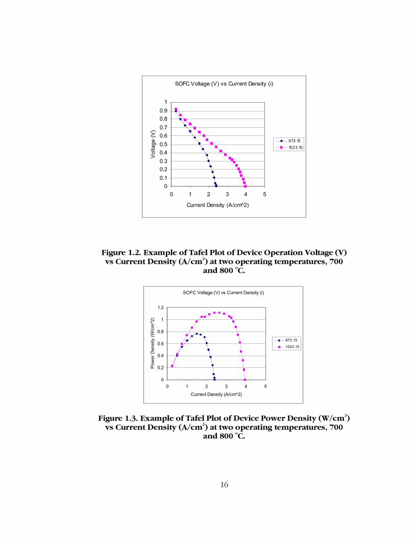
16
Figure 1.2. Example of Tafel Plot of Device Operation Voltage (V) vs Current Density (A/cm2) at two operating temperatures, 700
and 800 oC.
Figure 1.3. Example of Tafel Plot of Device Power Density (W/cm2) vs Current Density (A/cm2) at two operating temperatures, 700
and 800 oC.
SOFC Voltage (V) vs Current Density (i)
0
0.2
0.4
0.6
0.8
1
1.2
0 1 2 3 4 5
Current Density (A/cm^2)
Pow
er D
ensi
ty (W
/cm
^2)
973.15
1023.15
SOFC Voltage (V) vs Current Density (i)
00.10.20.30.40.50.60.70.80.9
1
0 1 2 3 4 5
Current Density (A/cm^2)
Volta
ge (V
)
973.151023.15

17
1.4 RESEARCH METHODOLOGY
1.4.1 Device Architecture
Within the scope of this research, two planar SOFC architectures are
currently investigated: anode supported and electrolyte supported cell
geometries, as shown in Figure 1.4. For this preliminary investigation,
standard materials are used and outlined in this figure.
Figure 1.4. SOFC Cell Architecture, materials and geometries used in this analysis.
SOFC Device Architecture
Anode
Electrolyte
Cathode
Anode:•Ni-Cermet•Thickness: ~.5-1mm
SOFC Stack:
•Area: 10x10 cm
Cathode:•Lathanum strontium manganite (LSM) •Thickness: ~50um
Electrolyte:•Yttria Stabilized Zirconia (YSZ) •Thickness: 10-150um anode supported; 150+um electrolyte supported

18
1.4.2 Device Fabrication Flow and Processes
The manufacturing flow modeled within this cost model is outlined in
Figure 1.5. This flow consists of 1) tape casting of the cathode and
anode layers 2) deposition of the electrolyte on either the cathode or
anode layer and 3) co-sintering of the anode, cathode and electrolyte
layers. The electrolyte deposition processes are varied to allow direct
comparison between processes. Three processes were selected for this
analysis based on the cost and thin film capability of the processes. The
processes used in this analysis are sputtering, screen printing and tape
casting.
Figure 1.5. Diagram of the manufacturing flow used in this analysis
SOFC Fabrication Process –Anode and Electrolyte Supported device
Anode CathodeTape Casting of Anode/Cathode
Deposition of Electrolyte
Co-sintering of stack
Electrolyte
Cathode
Electrolyte
Cathode
Anode
orElectrolyte
Anode

19
Sputtering, or PVD, is a process used widely in the semiconductor
industry to deposition very thin (<1um) films. The sputtering process
consists of Argon gas introduced into a high vacuum chamber as shown
in Figure 1.6. A radio frequency (RF) plasma is generated in the
chamber, directing the argon atoms toward a target consisting of the
deposition material. Atoms of the deposition material are ejected from
the target by a momentum transfer process [15]. These atoms are re-
deposited onto the deposition substrate surface. The process continues
until the desired thickness of the deposition (target) material has been
re-deposited on the substrate surface. Equipment and material costs for
the sputtering process are typically very high depending process
capability requirements. Film deposition capability and film quality for
sub-micron films is very good.

20
Figure 1.6. PVD-Sputtering Chamber Diagram
PVD-Sputtering Diagram
Vacuum pump
Target
Ar+ ions accelerated to target
Surface Atoms Ejected from Target
Gas inlet
Substrate (Area to be coated)
Cathode
RF Plasma/Magnetic Field
RF Signal

21
Tape Casting is a process used throughout the ceramic industry for
producing high quality, inexpensive film substrates. As shown in Figure
1.7, the tape casting equipment consists of a carrier tape, slip hopper
and doctor blade. As the carrier tape moves below the doctor blade, the
ceramic slip, a suspension of the deposition material incorporated with a
binder material, is deposited on the carrier tape. The distance from the
tip of the doctor blade as well as the carrier tape speed determines the
film thickness. Although tape casting is a very cost effective process,
process capability for films less than 5um is marginal, with very little
documented high volume manufacturing of less than 3um films.
Figure 1.7. Diagram of a Tape Casting System [61]
Tape Casting Overview(61)

22
Screen Printing, is a process by which an “ink” consisting of a
suspension of the deposition material and binder is forced through a
fine wire mesh, or printing frame, depositing the ink on the substrate
surface. An example of screen printing equipment and the printing
frame are shown in Figure 1.8. Screen printing is a moderately priced
process, with good process capability for 3-5um films.
Figure 1.8 Screen Printing Overview Diagram [62,63]
Screen Printing Overview [62,63]
Screen Printing Process (62) Printing Frame(63)

23
1.4.3 Cost Model Methodology
The cost model analysis consists of three steps as outlined in Figure 1.9:
1) the use of a device performance model to calculate the required film
thickness tolerances for a given operating temperature, maximum power
density and performance tolerances for each of these parameters, 2) the
calculation of the process yield at each layerfor the required film
thicknesses tolerances and 3) the overall cost to produce a cell using
data provided by steps 1) and 2).
Figure 1.9. Flow diagram of cost model analysis
SOFC Cost Model Diagram:
(3) Determine Per-Cell Costs Incorporating Process Yields
(1) Determine Fabrication Tolerances for required Device Performance • Layer Thickness Tolerances
(2) Determine Process Yields at Thickness Tolerances

24
1. Proceedings of the Electrochemical Society, SOFC VI (1999), pp.127-320.
2. Proceedings of the Electrochemical Society ,SOFC VI (1999), pp. 320-540.
3. Proceedings of the Electrochemical Society ,SOFC VII (2001), pp. 275-769.
4. Proceedings of the Electrochemical Society , SOFC VII (2001), pp. 875-1089.
5. Larminie, J., Dicks, A.,”Fuel Cell Systems Explained”, Wiley and Sons, NY (2001), pp.124-180.
6. Primdahl, S., Jorgensen, M.J., Bagger, C., Kindl, B., “Thin Supported SOFC”, SOFC VI (1999), pp.793-802.
7. Pham, A., Chung, B., Haslam., Lenz, D., See, E., Glass, R., “Demonstration of high power density planar solid oxide fuel cell stacks,” SOFC VII (2001), pp.149-154.
8. Murata, K., Okawa, H.,Ohara, S., Fukui, T., Yoshida, H., Inangaki, T., Miura, K., “Preparation of LSGM Electrolyte Film by Tape Casting Method”, SOFCVII (2001), pp.368-374
9. Fukunaga, H., Arai, C., Wen, C., Yamada, K., “Thermal Expansion and Cathode Behavious of YSCF as SOFC Cathode”, SOFCVII (2001), pp.449-457.
10. Ralph, J.M., Vaughey, J.T., Krumpelt, M., “Evaluation of Potential Cathode Materials for SOFC Operation Between 500-800oC”, SOFC VII (2001), pp.466-475.
11. Kim, J.W., Virkar, A.V., “The Effect of Anode Thickness of the Performance of Anode Supported Solid Oxide Fuel Cells,” SOFC VI, 1999, pp 830-839.
12. “Haart, L.G.J., Mayer, K., Stimming, U., Vinke, I.C., “Operation of anode-supported thin electrolyte film solid oxide fuel cells at 800oC and below,” Journal of Power Sources 71 (1998) pp.302-305.
13. 14. Chan, S.H., Khor, K.A., Xia, Z.T., “ A complete polarization model
of a solid oxide fueld cell and its sensitivity to the change of cell

25
component thickness,” Journal of Power Sources 93 (2001) pp.130-140.
15. Will, J., Mitterdorfer, A., Kleinlogel, C., Perednis, D., Gaukler, L.J., “Fabrication of thin electrolytes for second-generation solid oxide fuel cells,” Solid State Ionics 131 (2000) pp.79-96.
16. Yoshida, T., Okada, T., Hamatani, H., Kumaoka, H., “Integrated fabrication process for solid oxide fuel cells using novel plasma spraying”, Plasma Sources Sci. Technology 1 (1992) pp. 195-201.
17. Zhitomirshky, I., Petric, A., “Electrophorectic deposition of ceramic materials for fuel cell applications,” Journal of the European Ceramic Society 20 (2000), pp.2055-2061.
18. Will, J., Hruschkla, M.K.M., Gubler, L., Gauckler, L.J., “Electrophorectic Deposition of Zirconia on porous Anodic Substrates,” J. Am. Ceram. Soc., 84 [2] (2201) pp.328-32.
19. Huebner, W., Reed, D.M., Anderson, H.U., “Solid Oxide Fuel Cell Performance Studies: Anode Development ,” SOFC IV (1999) pp.503-512.
20. Virkar, A.V., Chen, J., Tanner, C., Kim, J., “The role of electrode microstructure on activation and concentration of polarizations in solid oxide fuel cells”, Solid State Ionics 131 (2000) pp.189-198.
21. [D14] WWW.globalte.com/fcmore-mail.htm 22. Arthur D. Little, Inc., “Assessment of Planar Solid Oxide Fuel Cell
Technology,” Report to DOE FETC, October 1999. 23. Virkar, A.V., “Low-Temperature, Anode-Supported High Power
Density Solid Oxide Fuel Cells with Nanostructured Electrodes,” Quarterly Technical Report to Contract Number DE-AC26-99FT40713, submitted April 7, 2000.
24. Karakoussis, V., Brankdon, N.P., Leach, M., van der Vorst, R., “ The Environmental Impact of Manufacturing Planar and Tubular Solid Oxide Fuel Cells,” Journal of Power Sources 101 (2001) pp. 10-26.
25. Singhal, S.C., “Science and Technology of Solid-Oxide Fuel Cells,” MRC Bulletin, March 2000 pp.16-21.
26. Godfrey, B., Foger, K., Gillespie, R., Bolden, R., Badwal, S., “ Planar Solid Oxide Fuel Cells: The Austraian Experience and Outlook,” Journal of Power Sources 86(2000) pp. 68-73.
27. Gardner, F.J., Day, M.J., Brandon, N.P., Pashley, M.N., Cassidy, M.,” SOFC Technology Development at Rolls-Royce,” Journal of Power Sources 86 (2000) pp.122-129.
28. Haart, L., Mayer, K., Stimming, U., Vinke, I., “Operation of anode-supported thin electrolyte film solid oxide fuel cells at 800 oC and below,” Journal of Power Sources 71 (1998) 302-305.

26
29. Charpentier, P., Fragnaud, P., Schleich, D.M., Gehain, E.,” Preparation of Thin film SOFCs Working at Reduced Temperature,” Solid State Ionics 135 (2000) pp.373-380.
30. Ohrui, H., Matsushima, T., Hirai, T., “ Performance of a Solid Oxide Fuel Cell Fabricated by Co-Firing,” Journal of Power Sources 71 (1998) 185-189.
31. Peng, Z., Liu, M., “Preparation of Dense Platinum-Yttria Stabilized Zirconia and Yttria Stabilized Zirconia Films on Porous La0.9Sr0.1MnO3 (LSM) Substrates,” Journal of the American Ceramic Society, 84 (2001) pp. 283-288.
32. Gorte, R., Kim, H., Vohs, J., “Novel SOFC anodes for the direct electrochemical oxidation of hydrocarbon,” Journal of Power Sources 4639 (2002) pp. 1-6.
33. Hart, N., Brandon, N., Day, M., Lapena-Rey, N., “ Functionally graded composite cathodes for solid oxide fuel cells,” Journal of Power Sources 4648 (2002) pp. 1-9.
34. Huebner, W., Anderson, H., “ Anode, Cathode and Thin Film Studies for Low Temperature SOFC’s,” Final Report to DOE DE-FG26 98FT40487, 10/31/1999, University of Missouri- Rolla.
35. Schafer, W., Koch, A., Herold-Schmidt, U., Stolten, D., “ Materials, interfaces and production techniques for planar solid oxide fuel cells,” Solid State Ionics 86-88 (1996) pp. 1235-1239.
36. Lang, M., Henne, R., Schaper, S., Schiller, G., “Development and Characterization of Vacuum Plasma Sprayed Thin Film Solid Oxide Fuel Cells,” Journal of Thermal Spray Technology 10(4) 2001 pp. 618-625.
37. Okamua, K., Aihara, Y., Ito, S., Kawasaki, S., “Development of Thermal Spraying-Sintering Technology for Soid Oxide Fuel Cells,” Journal of Thermal Spray Technology 9(3) 2000 pp. 354-359.
38. Swartz, S.L., Dawson, W.J., “Composite Ceria Electrolytes,” www.nextechmaterials.com.
39. Xia, C., Miu M., “Low-temperature SOFCs based on Gd0.1 Ce0.9 O1.95
fabricated by dry pressing,” Solid State Ionics 144 (2001) pp. 249-255.
40. Visco, S., Jacobson, C., De Jonghe, L., “High Performance SOFCs Operating at Temperatures Below 700 o C,” Materials Science Division, Lawrence Berkeley National Laboratory, Technical Bulletin ( 1998). [E16]
41. Fukui, T., Ohara, S., Murata, K., Yoshida, H., Miura, K., Inagaki, T., “Performance of intermediate temperature solid oxide fuel cells with LA(Sr)Ga(Mg)O3 electrolyte film,” Journal of Power Sources 4643 (2002) pp. 1-4.

27
42. Ohara, S., Maric, R., Zhang, X., Mukai, K., Fukui, T., Yoshida, H., Inangaki, T., Miura, K., “High performance electrodes for reduced temperature solid oxide fuel cells with doped lanthanum gallate electrolyte I. Ni-SDC cermet anode,” Journal of Power Sources 86 (2000) pp. 455-458.
43. He, H., Huang, X., Chen L., “ Sr-doped LaInO3 and its possible application in a single layer SOFC, “ Solid State Ionics 130 (2000) pp. 183-193.
44. Van herle, J., Horita, T., Kawada, N., Sakai, N., Yokokawa, H., Dokiya, M., “Low Temperature Fabrication of (Y,Gd,Sm)-doped ceria electrolyte,” Solid State Iionics 86-88 (1996) pp. 1255-1258.
45. Eguchi, K., Hatagishi, T., Arai, H., “ Power generation and steam electrolysis characteristics of an electrochemical cell with a zirconia- or ceria based electrolyte,” Solid State Ionics 86-88 (1996) pp 1245-1249.
46. http://www.nextechmaterials.com/products.htm 47. Steele, B., “Survey of materials selection for ceramic fuel cells II.
Cathodes and anodes,” Solid State Ionics 86-88 (1996) pp. 1223-1234.
48. Young, J.L., Etsell, T.H., “Polarized electrochemical vapor deposition for cermet anodes in solid oxide fuel cells,” Solid State Ionics 135 (2000) pp. 457-462.
49. Tang, E., Etsell, T., Ivey, D., “A New Vapor Deposition Method for Form Composite Anodes for Solid Oxide Fuel Cells,” Journal of the American Ceramic Society, 83 (7) pp. 1626-32 (2000).
50. Ucnimoto, Y., Tsutsumi, K., Ioroi, T., Ogumi, Z., Takehara, Z., “Reactions in Vapor-Phase Electrolytic Deposition for Preparting Yttria-Stabilized Zirconia Thin Films,” Journal of the American Ceramic Society, 83 (1) pp. 77-81 (2000).
51. Hart, N., Brankdon N., Shemilt, J., “Environmental Evaluation of ThickFilm Ceramic Fabrication Techniqies for Solid Oxide Fuel Cells,” Materials and Manufacturing Processes, Vol. 15, No.1 pp. 47-64, 2000.
52. Hwang, H.J., Towata, A., Awano, M., “Fabrication of Lanthanum Manganese Oxide Thin Films on Yttria-Stabilized Zirconia Sustrates by a Chemically Modified Alkoxide Method,” ,” Journal of the American Ceramic Society, 84 (10) pp. 2323-2327 (2001).
53. Nagamoto, H., Ikewaki, H., “Preparation of YSZ Thin Film On Porous Electrode of SOFC,” Proceedings from the Materials Research Symposium volume 547, 1999.
54. Yoshida, T., Okada, T., Hamatani, H., Kumaoka, H., “Integrated fabrication process for solid oxide fuel cells using novel plasma

28
spraying,” Plasma Sources Science and Technology 1 (1992) pp. 195-201.
55. Kang, H., Taylor, P., “Direct Production of Porous Cathode Material (La1-xSrxMnO3) using a Reactive DC Thermal Plasma Spray System,” Journal of Thermal Spray Technology 10(3) pp. 526-531 (2001).
56. Gitzhofer, F., Boulos, M., Heberlein, J., Henne, R., Ishigaki, T., Yoshia, T., “Integrated Fabrication Processes for Solid Oxide Fuel Cells Using Thermal Plasma Spray Technology,” MRS Bulletin, July 2000, pp. 38-42.
57. Hobein, B., Tietz, F., Stover, D., Kreutz, E., “Pulsed laser deposition of yttria stabilized zirconia for solid oxide fuel cell applications,” Journal of Power Sources 4572 (2001) pp. 1-4.
58. Mister, R.E., Twiname, E.R., Tape Casting, Theory and Practice, The American Ceramic Society (2000), pp 190-191.
59. Ishahara, T., Shimose, K., Kudo, T., Nishiguichi, H., Akbay, T., Takita, Y., “Preparation of Yttria-Stabilized Zirconia Thin Films of Strontium-Doped LaMnO3 Cathode Substrates via Electrophoretic Deposition for Solid Oxide Fuel Cells”, Journal of the American Ceramic Society, 83 (8) pp. 1921-27 (2000).
60. Xia, C., Liu, M., “Low –temperature SOFCs based on Gd0.1Ce0.9O1.95
fabricated by dry pressing,” Solid State Ionics 144 (2001) 249-255. 61. www.cranfidle.ac.uk/sims/materials/processing/tcintro.htm 62. Sefar Handbook for Screen Printers, 1999 63. www.dek.com/homepage.nsf/dek/screenprint_medium.html

29

30
CHAPTER 2. DEVICE PERFORMANCE MODEL
Definition of Terms:
P = power density (W/cm^2) i= current density ( A/cm^2) io= effective exchange current density(A/cm^2) V= Voltage (Volts) Eo= open circuit voltage (Volts)
R= gas constant (J/mol deg) T=Temperature (K) F= Faraday constant (C/mol) a =-RT/4αF * ln io
b =-RT/4αF po
H2 = partial pressure of hydrogen at the anode/electrolyte interface(atm) po
H2O = partial pressure of water vapor in the fuel(atm) po
O2 = partial pressure of oxygen in the oxidant (atm)
Ri = area specific resistance of the electrolyte (Ohm cm^2)
= effct
e
eeffctli RlRR +=+=
σeR where
)1( ve
cteffct V
BRR
−=
σ
ias=anode limiting current density (A/cm^2) = a
aeffoH
RTl
DFp ,22
aeffD , = effective diffusion coefficient on the anode side cm^2/s
al = anode thickness, cm el = electrolyte thickness, um Rct = intrinsic (area specific) charge transfer resistance, (Ohm cm^2) σe = ionic conductivity of the electrolyte (S/cm) Vv=layer porosity B=microstructural dimension (grain size of material) (um)

31
2.1 MODEL DERIVATION:
There are several purely theoretical device performance models [3,1] in
the literature as well as performance models where specific equation
parameters such as ionic resistivity, current densities, and diffusion
coefficients are derived from experimental data fitted to a theoretical
model [2,4,5]. The goal of this work was to combine appropriate
theoretical parameters and fitted parameters taken from the literature to
create a general polarization model as a function of anode, cathode
and electrolyte thickness.
This general model would be simplified by eliminating parameters or
substituting constants for parameters where literature supported. This
simplified polarization model could then be used to calculate the
required layer thicknesses and thickness tolerances for given device
operating temperatures and device maximum power density
requirements.

32
2.1.1 General Polarization Model
The difference between actual and ideal operating voltage for a SOFC is
known as polarization or over-potential. A general polarization model
as a function of current density can be described using the following
expression [3,4]:
cathodeconcanodeconccathodeactanodeActohmoViV ,,,,)( ηηηηη −−−−−=
(1)
where:
V0 is the reversible open circuit voltage, expressed
using the Nernst equation:
Vo = )ln(2
ln2 2
2/122
OH
OH
PPP
FRTK
FRT − (2)
cathodeactanodeAct ,, ,ηη represent the activation losses occurring due to the
slowness of the reaction rate taking place on the
surface of the electrode [4]. A proportion of the
voltage generated is lost in driving the chemical
reaction that transfers the electrons to or from the
electrode.

33
Activation losses are modeled using two separate
equations, depending on the level of polarization
activation [3].
Under high activation polarization, the losses can be
modeled by the Tafel equation:
=actη activation polarization = iba ln+ (3)
where oiF
RTa ln4α
≈ and F
RTbα4
≈
Under low activation polarization, the losses can be
modeled using the linear current potential relationship:
iFin
RT
oe
act =η
Within the model used in this analysis, high
polarization concentrations are assumed, limiting the
model accuracy at lower polarization concentrations.
ohmη represents the ohmic loss resulting from the electrical
resistance within the electrodes, primarily due to
resistance to flow of electrons through the electrolyte

34
material. The size of this loss is directly proportional to
current flow, adjusted to units of current density:
lohm i eR=η where Rel = electrolyte area specific
resistance = e
elσ
Modeling by Tanner[7], et al, indicates that the reaction
zone is actually spread out into the electrode some
distance from the electrolyte, electrode interface.
Tanner defined an additional parameter, the effective
charge transfer resistance, Rct
eff , in terms of
microstructural parameters of the electrode, intrinsic
charge transfer resistance, Rct , the ionic conductivity of
the electrolyte, σe , and the electrode thickness. Kim,
et. al. shows that the reaction zone can be
represented by the sum of the electrolyte area specific
resistance, leR , and the effective charge-transfer
resistance, effctR [2]:

35
effct
e
eeffctli RlRR +=+=
σeR (5)
Where )1( ve
cteffct V
BRR
−=
σ
cathodeconcanodeconc ,, ,ηη represent the concentration losses resulting from
the change in concentration of the reactants at the
surface of the electrodes as the fuel is used (4).
cathodeconc,η = )1ln(4 csi
iF
RT − (6)
anodeconc,η = )1ln(2
)1ln(2 0
2
02
asOH
H
as ipip
FRT
ii
FRT +−− (7)
The ics and ias terms represent the cathode and anode
limiting densities which occur when the partial
pressure of hydrogen at the anode or
cathode/electrolyte interface is nearly zero. Both terms
are related to the effective binary diffusion coefficients,

36
Deff,c , for the cathode (between O2 and N2) and Deff,a ,
for the anode (between H2 and H2O) as well as the
electrode thicknesses, lc and la , as follows [1]:
c
oO
ceffoO
cs
RTlppp
DFpi
−=
)(
4
2
,2
where c
NOcvceff
DVDτ
2,,
2 −= (8)
a
aeffoH
asRTl
DFpi ,22
=
where a
OHHcvaeff
DVDτ
22,,
−= (9)
Utilizing work by Kim, et. al. [1 , 2], equations 2-9 were substituted into
equation (1) to relate the operating voltage, V, to the current density, i,
as follows:
)1ln(2
)1ln(2
)1ln(4
)ln()( 02
02
asOH
H
ascsio
ipip
FRT
ii
FRT
ii
FRTibaiREiV +−−+−+−−−=
(10)

37
Equation (10) was further simplified by examining cell geometries used
in this analysis. For anode and electrolyte supported cells, lc << la , and
equation (10) is not sensitive to ics. As a result, equation (10) can be
reduced to:
)1ln(2
)1ln(2
)ln()( 02
02
asOH
H
asio
ipip
FRT
ii
FRTibaiREiV +−−+−−−= (11)
and ( )
+
+−
++−=ii
ppiiF
RTibR
diidV
as
H
OHasi
02
02
224
)( (12)
2.1.2 Power Density Model
The power density of a cell is given by:
)()( iiViP = (13)

38
In this analysis, our goal was to determine the maximum power density
for a given range of current densities. To do this, equation (13) was
differentiated with respect to ,i and set equal to zero:
)()( iVdi
idVididP += = 0, (14)

39
Substituting equations (11) and (12) into equation (14) yields equation
(15):
0)1ln(1ln2
))ln(1(2 02
02
02
02
=
+−
++
−+
−+−+−−=
asOH
H
asH
OHasasio
ipip
iip
pi
ii
iii
FRTibaiRE
didP
To determine the maximum power density for given set of cell
parameters, Equation (15) is solved iteratively for maxii = . The value for
maxi is then substituted into equation (11) to obtain the voltage V(i) at
the maximum power density. V(i) and maxi are substituted in equation
(13) to determine the maximum power density P(i).

40
4.1.3 Electrolyte Resistance Model
A linear model for electrolyte resistance was created using literature data
from Mutsitami, et al [5]. Figure 2.1 represents the natural log of the
electrolyte resistance as a function of temperature (oK) [5] for thin film
YSZ. A linear fit of ln R = -0115(Temp) + 15.238 is used in the
performance model to calculate the electrolyte ionic resistivity of the
YSZ as a function of temperature.
Figure 2.1 Natural Log of the Ionic Resistivity as a Function of Temperature
y = -0.0115x + 15.238R2 = 0.9966
02468
700 800 900 1000 1100Temperature (deg K)
ln(R
)

41
2.2 RESULTS AND DISCUSSION
Maximum power densities were calculated using the model and
methodology outlined in Section 2.1. The basic assumptions used to
simplify the model were 1) neglecting cathodic influences due to cell
geometries as discussed in section
Table 2.1 Cell Parameters used in Performance Model
Table 1: Parameters used in calculations
Constants:value
Eo 1R (gas constant) 8.314F (Faraday constant) 96485poH2 (atm) 0.095poH20 (atm) 0.005alpha 0.5 **exp data indicates .5 is good estimate
io (A/cm^2) 0.1**[1]should be constant for same material + density
Deff (a) (cm^2/sec) 0.45**[2,3]should be constant for same material + density + gas pressures
BRct/(1-Vv) 0.0001**derived from exp data [1,2] should be constant for same material + density
Variables:
T (temp deg K)Anode thickness (cm)Electrolyte thickness (um)i current density (A/cm^2)

42
2.1, 2) assuming operation at high polarization concentrations as
discussed in section 2.1 and 3) setting material specific property
parameters equal to constants.or groups of constants as outline in table
2.1. The net effect of these assumptions on the general polarization
model is a linearization of the Tafel performance curves as compared to
curves generated by experimental data. The effect of these assumptions
on the accuracy of the model in calculating maximum power density is
tested against experimental results in Figure 2.2 .
Figure 2.2 shows maximum power density results calculated compared
to results from experimental data presented in references 1-2, 8-11.
Correlation to the literature results is very good throughout the range of
power densities, with an R-squared value of .9541.

43
Figure 2.2. Calculated versus Experimental Maximum Power Densities
In order to test the model against expected variable effects as well as aid
in the understanding of the interactions between model variables, 2-
dimensional graphs were created and are shown as Figures 2.3-2.7.
These graphs are described in Sections 2.2.1-2.2.2.
2.2.1 Anode layer thickness variation effects
Figure 2.3 shows the decrease in maximum power density as anode
thickness increases across a range of operation temperatures at a
y = 1.0375xR2 = 0.9541
0
0.5
1
1.5
2
2.5
0 0.5 1 1.5 2 2.5
Experimental max power density (W/cm^2)
Cal
cula
ted
max
pow
er d
ensi
ty (W
/cm
^2)
Source (1)Source (2)Source (8)Source (9)Source (10)Source (11)
Linear ( )

44
constant electrolyte thickness of 10um. This relationship between
power density and anode thickness is consistent with experimental
results obtained by Kim, et al [1], and is due to the increase in the
resistivity of the anode layer. Note that this effect decreases in intensity
as the operation temperature is decreased and electrolyte layer
resistance becomes the primary device performance limiter.
A similar effect is depicted in Figure 2.4, which shows the increase in
operating temperature as anode thickness increases over a range of
power densities. In this figure, anode thickness is shown to have a
much more significant impact on device operating temperature at higher
power densities. This effect is also to some extent represented in
experimental data from Kim, et. al, [1], and can be attributed to the
decrease in anode current limited density as the anode thickness is
reduced.

45
Figure 2.3 Maximum Power Density versus Anode Thickness varying Operation Temperatures (oC), electrolyte thickness fixed
at 10um.
0
0.5
1
1.5
2
2.5
0 0.05 0.1 0.15 0.2 0.25
Anode Thickness (cm)
Max
Pow
er D
ensi
ty (W
/cm
^2)
650700750800

46
Figure 2.4 Device Operation Temperatures (oC) versus Anode Thickness varyng Maximum Power Densities (W/cm2), electrolyte
thickness fixed at 10um.
500
600
700
800
900
1000
1100
0 0.05 0.1 0.15 0.2 0.25
Anode Thickness (cm)
Ope
ratin
g Te
mp
deg
C
0.250.511.251.4

47
2.2.2 Electrolyte layer thickness variation effects
The variation in maximum power density and operating temperature as
electrolyte thickness increases is shown, respectively, as Figures 2.5 and
2.6. This effect is shown across a range of temperatures (Figure 2.5) and
power densities (Figure 2.6) , with anode thickness held as a constant at
1mm. The non-linear nature of the decrease in maximum power density
and increase in operating temperature as electrolyte thickness increases
is due to the non-linear relationship between the electrolyte area specific
resistance, leR , the effective charge transfer resistance, effctR , and the
electrolyte thickness. Note that this effect is consistent across the power
density and the temperature range shown in the graph.
The overall electrolyte thickness variation impact to both maximum
power density and operating temperature is shown in Figure 2.7. The
most significant impact to both power density and operating
temperature is seen at the lower electrolyte thicknesses. It can also be
seen that at a constant operating temperature the power density for a
given device can be manipulated through a large range of maximum
power densities by decreasing the electrolyte thickness. Similarly, a
constant maximum power density can be achieved across a wide range
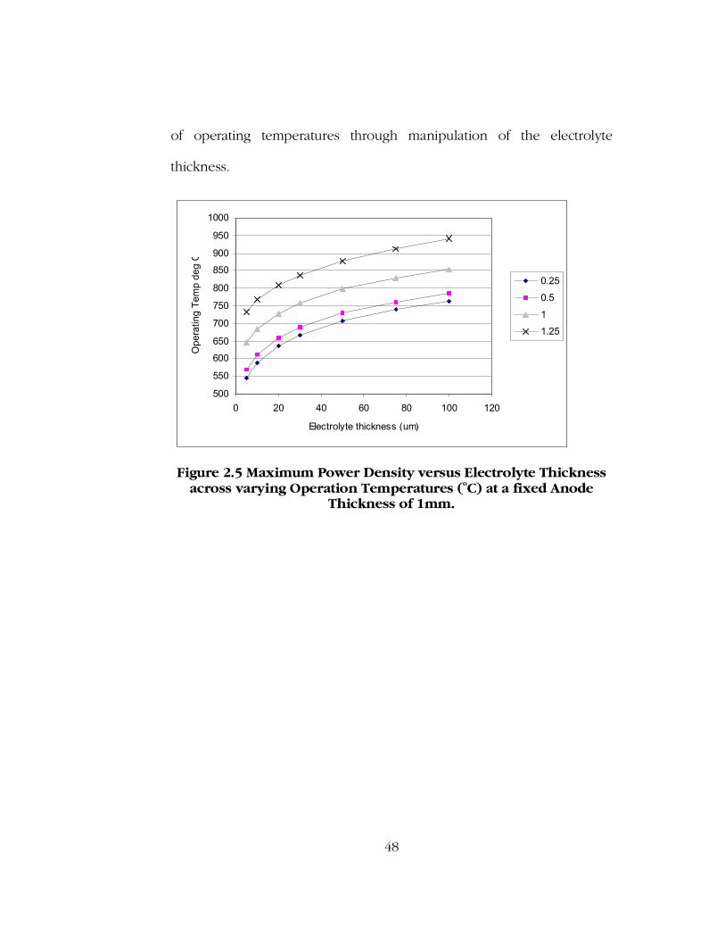
48
of operating temperatures through manipulation of the electrolyte
thickness.
Figure 2.5 Maximum Power Density versus Electrolyte Thickness across varying Operation Temperatures (oC) at a fixed Anode
Thickness of 1mm.
500
550
600
650
700
750
800
850
900
950
1000
0 20 40 60 80 100 120
Electrolyte thickness (um)
Ope
ratin
g Te
mp
deg
C
0.25
0.5
1
1.25

49
Figure 2.6 Device Operating Temperature versus Electrolyte Thickness at varying Power Densities (W/cm2) using an anode
thickness of 1mm.
0
0.25
0.5
0.75
1
1.25
1.5
1.75
2
2.25
0 20 40 60 80 100 120
Electrolyte thickness (um)
Max
Pow
er D
ensi
ty (W
/cm
^2)
650700750800

50
0
0.5
1
1.5
2
2.5
500 600 700 800 900
Operating Temp (deg C)
Max
Pow
er D
ensi
ty (W
/cm
^2)
51020305075100
Figure 2.7. Operating Temperature versus Maximum Power Density at varying Electrolyte Thickness (um) using an Anode
Thickness of 1mm.

51
Sources:
1. Kim, J.W., Virkar, A.V., “The Effect of Anode Thickness of the Performance of Anode Supported Solid Oxide Fuel Cells,” SOFC VI, 1999, pp 830-839.
2. Kim, J.W., Virkar, A.V., Fung, K.Z., Mehta, K., Singhal, S.C., “Polarization Effects in Intermediate Temperature, Anode Supported Solid Oxide Fuel Cells,” Journal of the Electrochemical Society, 146 (1), 1999, pp. 69-78.
3. Chan, S.H., Khor, K.A., Xia, Z.T., “ A Complete Polarization Model of a Solid Oxide Fuel Cell and its Sensitivity to the Change of Cell Component Thickness,” Journal of Power Sources (93), 2001, pp. 130-140.
4. Larminie, J., Dicks, A., Fuel Cell Systems Explained, (2001) Wiley pp. 37-59.
5. Mizutani, Y., Kawai, K., Nomura, K., Nakamura, Y., Yamamoto, O., “Characteristics of Substrate Type SOFC Suing Sc-Doped Zirconia Electrolyte,” SOFC VI, 1999, pp 185-192.
6. SOFC VII (2001), pp. 936. 7. Tanner, C.W., Fung, K.Z., Virkar, A.V., Journal of the
Electrochemical Society (144), 1997, pp21-30. 8. Charpentier, P., Fragnaud, P., Schleich,D.M., Gehain, E., "
Preparation of thin film SOFCs working at reduced temperature", Solid State Ionics (135) , 2000, pp. 373-380.
9. Khandar, A., Elangovan, S., Hartvigsen, J., Rowley, D., Privette, R., Tharp, M.,"Status of SOFCo's Planar SOFC Development", SOFC VI, 1999, pp. 88-94.
10. Virkar, A.V., Chen, J., Tanner, C.W., Kim, J.W., " The role of electrode microstructure on activation and concentration polarizations in solid oxide fuel cells", Solid State Ionics (131), 2000, pp. 189-198.
11. Okamura, K., Aihara, Y., Ito, S., Kawasaki, S., Development of Thermal Spraying-Sintering Technology for Solid Oxide Fuel Cells", Journal of Thermal Spray Technology, Volume 9(3), 2000, pp. 354-359.

52
CHAPTER 3. PROCESS TOLERANCE MODEL
3.1. PROCESS TOLERANCE MODEL DERIVATION
For a given film deposition process, the film deposition rate will vary
across the deposition surface. This variation can be measured by
external measurement of film thickness at specific points across the
deposition surface upon completion of the film deposition to the target
thickness. For instance, if the target deposition thickness across a .3m
substrate is 10um, once film deposition has completed, the film
thickness may be measured incrementally across the substrate. From
these measurements, a standard deviation, or film thickness tolerance, at
the target film thickness can be determined.
( )1
1
2
−
−=∑
−
n
xxstdev
n
ii
where xi = measured film thickness n= number of measurements
x = mean of all film thickness measurements
Film thickness tolerances for a given deposition process may vary
greatly according to type of equipment, process setup and quality of
precursor material. Equipment manufacturers often provide thickness
standard deviation specifications formatted as a given film thickness

53
standard deviation over a thickness deposition range. For instance, over
a range of 5-80um, an equipment manufacturer may specify that their
equipment will produce films with less then +/-2 um standard deviations
of film thickness for given processing conditions. The absolute standard
deviation can be converted to a percentage of film thickness and fitted
to a function in the following form:
BessFilmThicknAstdev −= )(*% (2)
where A= Film thickness standard deviation *100 B= 1
The equipment manufacturer specified film thickness tolerances are
based on a process optimized for a wide range of film thicknesses and
are often well within the capabilities of the equipment. In practice, as
process and equipment settings are optimized for a given film thickness
target, typically the film thickness standard deviation can be reduced
considerably. As this film thickness standard deviation is reduced at
specified thickness, the model in equation 1 can be adjusted by
reduction of the constants A and B to fit the new film thickness standard
deviation setpoints.

54
3.2 RESULTS AND DISCUSSION
3.2.1 Standard Deviation Models
To fully understand process capability throughout process lifetime,
process tolerance models were created at three time periods during the
process lifetime: equipment setup, process optimization and at process
maturity. Constants for equipment setup are based directly on
equipment manufacturer specifications as noted. The film thickness
standard deviation information available in the literature is used to
derive constants for process optimization and process maturity. Analysis
is done for three processes: tape casting, screen printing and sputtering.
The constants used in the analysis at these three time periods are listed
in Table 1.
Figure 3.1-3.3 model the % standard deviation as a function of film
thickness for the processes using constants in Table 1.
Table 1. Constants A,B used in Figure 3.1.
A B A B A B Sources
Tape Casting 500 1 300 0.85 110 0.7 1,2,3,4Screen Printing 300 1 125 0.9 65 0.8 5,7Sputtering 100 1 15 0.6 2.5 0.15 6,8
Equipment Setup Process optimization Fully Mature Process

55

56
Figure 3.1. Tape Casting: Green Film %Stdev vs. Film Thickness (um) varying constants A,B per Table 1.
Figure 3.2. Screen Printing (50x50cm cell): Film %Stdev vs. Film Thickness (um) varying constants A,B per Table 1.
2.00
22.00
42.00
62.00
82.00
102.00
122.00
142.00
162.00
182.00
0 10 20 30 40 50 60
Film Thickness (um)
Film
% S
tdev
Equipment SetupProcess OptimizationProcess Maturity
0.00
20.00
40.00
60.00
80.00
100.00
120.00
0 10 20 30 40 50 60
Film Thickness (um)
Film
% S
tdev
Equipment Setup
Process Optimization
Process Maturity

57
0.005.00
10.0015.0020.0025.0030.0035.0040.0045.00
0 20 40 60
Film Thickness (um)
Film
% S
tdev
Equipment Setup
Process Optimization
Process Maturity
Figure 3.3. Sputtering: Film %Stdev vs. Film Thickness (um) varying constants A,B per Table 1.
Film thickness standard deviation specification as Film %stdev is
modeled to decrease significantly as the process matures from
Equipment setup through to process maturity for thinner film
thicknesses. The greatest impact is seen at thinner film thickness
setpoints, where greater opportunity typically exists for process
optimization.
In practical application, a range of film thicknesses would be targeted
for process optimization, and constants A,B derived through curve fit to
process optimization results.

58
3.2.2 Process Yield Loss Calculation
The standard deviation is calculated at a nominal thickness using
equation 2 and constants detailed in Table 1. The film thickness is
assumed to be normally distributed, and the probabilities for the
minimum and maximum acceptable film thicknesses are calculated
based on the nominal thickness and standard deviation values. These
probabilities are converted to a percentage upper and lower yield loss
for each layer. Figure 3.4-3.6 show the variation in process yield for all
three processes as a function of film thickness, varying constants A and
B over process maturity. The allowable film thickness range is set to +/-
20% of the nominal thickness. Analysis is done for three processes: tape
casting, screen printing and sputtering. All process show significant yield
improvement over process lifetime.

59
Figure 3.4 Tape Casting: Process Yield Loss as a function of film thickness over process maturity.
0
20
40
60
80
100
0 20 40 60
Film Thickness (um)
Proc
ess
Yiel
d Lo
ss (%
)
EquipmentSetupProcessOptimizationMatureProcess

60
Figure 3.5 Screen Printing (250 cm^2 cell): Process Yield Loss as a function of film thickness over process maturity.
0
20
40
60
80
100
0 20 40 60
Film Thickness (um)
Proc
ess
Yiel
d Lo
ss (%
)
EquipmentSetupProcessOptimizationMatureProcess

61
Figure 3.6 Sputtering: Process Yield Loss as a function of Film Thickness over process maturity.
0102030405060708090
0 20 40 60
Film Thickness (um)
Proc
ess
Yiel
d Lo
ss (%
)
EquipmentSetupProcessOptimizationMatureProcess

62
3.2.2 Device Performance Impact on Process Yield
Within the cost model, the device performance requirements ultimately
determine process yields at each layer. As outlined in Chapter 2, as
maximum power density requirements increase, thinner film thicknesses
and tighter film thickness tolerances are required to meet these device
performance goals.
Power density and temperature setpoints and tolerance ranges are used
to calculate nominal, minimum and maximum layer thicknesses. The
thickness tolerances for each layer are used to model processing yields
for that layer. cell processing yield are calculated by combining process
yield for all layers. The overall impact of device performance tolerances
on cell process yield or process lifetime is represented in Figures 3.7-
3.12. These graphs represent cell processing yield using tape casting
for anode and cathode layers, and the indicated process (tape casting,
screen printing, sputtering) for electrolyte layers. A fixed 5% yield loss is
assumed for cell the cell co-sintering process.
Figures 3.7-3.12 show the significant yield improvement over process
lifetime for all processes. This improvement is shown to be greatest
lower operation temperatures and higher power densities due to thinner
film and tighter film thickness tolerance requirements.
Comparing the process yield for all three processes at lower operation
temperatures and higher power densities indicates that although
sputtering shows ~10% greater process yield during equipment setup, as

63
the tape casting and screen printing processes are optimized, process
yields become more comparable. Process yield differences between all
three process reduce to ~5% gap at 700 o C operating temperatures and
1 W/cm2 operation temperatures.

64
Figure 3.7 Tape Casting: Cell Process Yield vs. Device Operation Temperature Range, Maximum Power Density = 1.0 W/cm2
Figure 3.8 Screen Printing: Cell Process Yield vs. Device Operation Temperature Range, Maximum Power Density = 1.0 W/cm2
50.00%
55.00%
60.00%
65.00%
70.00%
75.00%
80.00%
85.00%
90.00%
95.00%
600 700 800 900 1000
Device Operation Temperature (deg C)
Stac
k Pr
oces
s Yi
eld
(%)
Process MaturityProcess OptimizationEquipment Setup
50.00%
55.00%
60.00%
65.00%
70.00%
75.00%
80.00%
85.00%
90.00%
95.00%
600 700 800 900 1000
Device Operation Temperature (deg C)
Stac
k Pr
oces
s Yi
eld
(%)
Process MaturityProcess OptimizationEquipment Setup

65
Figure 3.9 Sputtering: Cell Process Yield vs. Device Operation Temperature Range, Maximum Power Density = 1.0 W/cm2
Figure 3.10 Tape Casting: Cell Process Yield over Device Maximum Power Density Range (W/cm2), Device Operating Temp = 650 oC
50.00%
55.00%
60.00%
65.00%
70.00%
75.00%
80.00%
85.00%
90.00%
95.00%
600 700 800 900 1000
Device Operation Temperature (deg C)
Stac
k Pr
oces
s Yi
eld
(%)
Process MaturityProcess OptimizationEquipment Setup
50.00%
55.00%
60.00%
65.00%
70.00%
75.00%
80.00%
85.00%
90.00%
0.3 0.5 0.7 0.9 1.1 1.3
Device Maximum Power Density (W/cm^2)
Stac
k Pr
oces
s Yi
eld
(%)
process maturityprocess optimizationequipment setup
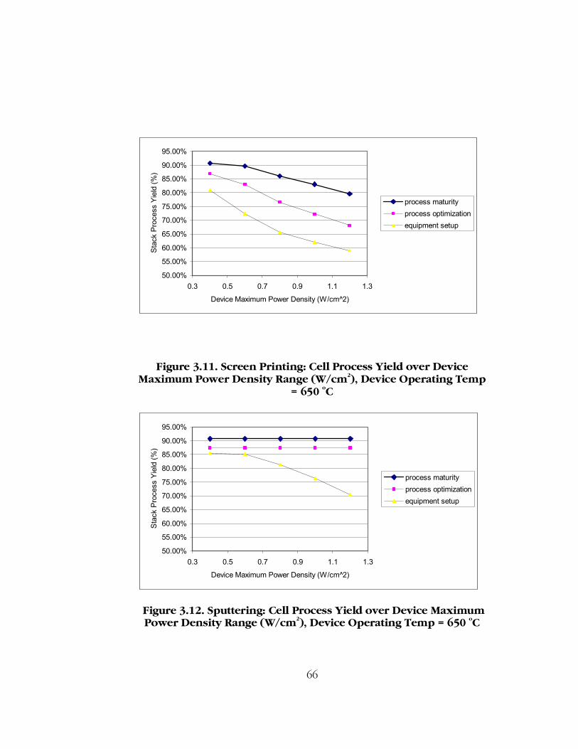
66
Figure 3.11. Screen Printing: Cell Process Yield over Device Maximum Power Density Range (W/cm2), Device Operating Temp
= 650 oC
Figure 3.12. Sputtering: Cell Process Yield over Device Maximum Power Density Range (W/cm2), Device Operating Temp = 650 oC
50.00%
55.00%
60.00%
65.00%
70.00%
75.00%
80.00%
85.00%
90.00%
95.00%
0.3 0.5 0.7 0.9 1.1 1.3
Device Maximum Power Density (W/cm^2)
Stac
k Pr
oces
s Yi
eld
(%)
process maturityprocess optimizationequipment setup
50.00%
55.00%
60.00%
65.00%
70.00%
75.00%
80.00%
85.00%
90.00%
95.00%
0.3 0.5 0.7 0.9 1.1 1.3
Device Maximum Power Density (W/cm^2)
Stac
k Pr
oces
s Yi
eld
(%)
process maturityprocess optimizationequipment setup

67
Sources:
1. http://www.aem-usa.com/pages/process/sl2104-2109spec.pdf 2. www.cicorel.ch/soldermaskrtr.htm 3. Equipment specification for Accucoat Screen Printer, technical
bulletin E2. 4. Sefar Handbook for Screenprinters, 2/ 1999. 5. Mister, R.E., Twiname, E.R., Tape Casting, Theory and
Practice, The American Ceramic Society (2000), pp 190-191. 6. Rao, R.A., et al, Appl. Phys. Letts. 69, 3911 (1996) 7. Batawi, E.,Weissen, U. Schuler, A., Keller, M. and Voisard, C.,
“Cell Manufacturing Processes At Sulzer Hexis”, SOFC VII (2001) pp. 140-147.
8. http://www.praxairsurfacetechnologies.com/MRC/mrc/docs/RE-Al-PLUS.html.

68
CHAPTER 4. PROCESS BASED COST MODEL
4.1 PROCESS BASED COST MODEL DEVELOPMENT
4.1.1 Introduction to Process Based Cost Models
Within a high volume manufacturing environment, there are many
factors that contribute to end of line, per piece cost. These factors range
from the direct purchasing costs for materials and equipment, equipment
and building depreciation, energy usage, as well as cost resulting from
employee wages and benefits. The complexity in creating a general, yet
accurate, cost model greatly increases due to interactions and
dependencies between variables.
For example, the per-piece material cost for a given production volume
is a function of the amount of material used to produce each piece. The
material amount is dependent not only on plate dimensions, but also on
material characteristics and the type of processing used to produce the
plates.
In a performance based cost model, plate dimensions are calculated
from device performance requirements, increasing the complexity of the
cost model. Therefore, in order to compute the amount of material used
and subsequent per-piece material costs, several calculated (i.e. plate
dimensions, scrap rates) as well as high level constant factors (i.e.

69
materials costs, material characteristics, process characteristics, device
performance requirements) must be known.
The major objectives of the preliminary cost model developed as part of
this analysis were to provide accurate evaluation of SOFC production
costs as a function of: 1) device performance requirements and 2)
multiple, integrated fabrication processes. Secondary objectives
included a user interface that would allow simplified, end-user
customization of cost model inputs and the ability to perform multi-input
sensitivity analyses.
4.1.2 Cost Model Methodology
The cost model was developed using a Microsoft Excel user interface
with Visual Basic Macros used to perform calculations and sensitivity
analysis.

70
Figure 4.1 Diagram of Cost Model Methodology
A diagram of the cost model information flow is presented as Figure 4.1.
In summary, the primary user inputs are specified within the cost model
worksheet. The required device architecture in the form of individual
component layer thickness tolerances are calculated based on the
required specifications using the device performance model outlined in
Chapter 2 of this thesis. Once the thickness tolerances are known,
individual layer processing yields are calculated based upon the process
tolerance model. These yields are used in conjunction with production
volume to calculate individual layer as well as SOFC cell material and
Cost Model Diagram
Calculate (per layer):
• Film thickness tolerances based on performance requirements
Calculate (per cell):
• Total Materials Cost• Total Equipment Cost• Production Volume/capacity• Cycle Time• Fabrication Yield
Primary User Inputs:• Operation Temperature• Maximum Power Density• Performance Tolerances • Layer processing• Layer material • Production Volume
Calculate (per layer):
• Layer yield (based on
film thickness tolerances)
• Material Costs• Equipment Costs

71
equipment costs, production volume, required capacity, manufacturing
cycle time and overall fabrication yield.
A detailed discussion of each portion of the cost model is presented in
sections 4.1.2.1-4.2.1.7.
4.1.2.1 Cost Model Inputs
Our goal was to create an accurate, yet simplified, cost model, including
as many significant cost factors as possible, without creating unnecessary
complexity. A secondary objective was to also allow for continued
simplified end-user customization of cost model inputs. To these ends,
high level constant factors were designated as primary and secondary
user inputs and were placed within the cost model so that they could be
easily accessed and modified to accommodate end used customization
and sensitivity analyses based around these factors.
These model inputs can be divided into two categories, 1) Primary user
inputs – inputs controlling or heavily dependent on the number of parts
produced, such as production volume, materials and equipment costs,
performance requirements and 2) Secondary User inputs – inputs that
may be fixed independently from production volume, such as wages
and benefits, cost of building space, electricity costs, and the capital
discount rates.
The primary and secondary user inputs used in this cost model analysis
are detailed in Figure 4.2. The primary user inputs controlling number of
parts produced include production volume, production capacity, and
average order size. Device performance requirements, plate dimensions
and nominal layer thicknesses are also considered to be primary user

72
inputs. Secondary user inputs include wage information, building and
electrical costs and downtime estimations.
Figure 4.2 Primary and Secondary User Inputs
Cost Model - Inputs
• Production volume• Production capacity• Average order size
•Anode/Cathode/Electrolyte/Substrate:
•Material•Process used•Plate dimensions•Layer nominal thickness
•Device Operating Temperature•Device Maximum Power Density
Primary User Inputs:
Other Inputs:Direct Wages (w/ benefits) Floor Space Multiplier Planned Downtime PaidWorking Days/Yr Price, Building Space Planned Downtime UnpaidShifts/Day Price of Electricity Unplanned DowntimeBase Shift Length Overhead Rate (%rent)
Capital Discount Rate

73
4.1.2.2 Cost Model Layer Thickness Tolerance Calculations
One of the most important aspects of a performance based cost model is
the use of modeling techniques to determine the cost basis of
performance requirements, i.e. determine the impact of the device
performance requirements to per-piece cost. The 1st step in this analysis
is to relate the performance requirements to materials and equipment
costs through the calculation of the required layer thickness tolerances
necessary to meet device performance requirements.
Layer thickness tolerances are calculated using the device performance
model outlined in Chapter 2. The diagram of this model is shown in
Figure 4.3. Note that in this analysis, electrolyte thickness is considered
to be the primary effect for device performance and anode thickness a
secondary effect. As a result, a nominal anode thickness is used to
initially calculate the electrolyte thickness tolerances. Device operation
temperature and a nominal anode thickness are entered into the
performance model. Electrolyte thickness is incremented until the
calculated power density is equivalent to the required power density. At
that point, the electrolyte thickness is set to the calculated value.
Minimum and maximum electrolyte and anode thickness requirements
are determined in a similar manner, using minimum and maximum
power density and operation temperature requirements as inputs. This
provides the range of allowable variation for electrolyte and anode
thicknesses to meet device operation temperature and power density
requirements. The process yield is then calculated for each layer based
on this variation using the process tolerance models as outlined in the
next section.

74
Figure 4.3 Layer thickness tolerance calculations
Cost Model – Layer thickness calculations
Inputs:• Operation Temperature• Maximum Power Density • Nominal Anode Thickness
Calculate Max Power Density (Pdmaxcalc) atTxcalcInputs:
• Constants from Table 1.• Layer thickness (Txcalc) = 1um (Pdmaxcalc) = (Pdmaxreqd) ??
Increment Txcalc+1um
Set Layer Thickness = (Txcalc)
equal Not equalCalculate Tx Min, Max based on Min, Max Power Density and Temperature Requirements

75
4.1.2.3 Cost Model Material Calculations
Per piece material costs are a function of the material costs (per weight)
and the amount or weight of material that is used. Material costs are
specified as part of the primary user inputs. The amount of material
used to manufacture each piece is calculated using material
characteristics, plate length and width dimension and layer thickness
tolerances. To simplify the model, plate length and width dimension are
also specified as part of the primary user inputs. Layer thickness
tolerances are calculated using device performance requirements as
outlined in section 4.1.2.2.

76
Figure 4.4 Diagram of Materials Calculations
Cost Model – Materials Calculations
Layer Material Inputs
Search Material Info (per layer):
• Density• Specific Heat• $/kg• Packing factor
Calculate (per layer, per plate):
• Material Volume• Material Mass• Surface Area• Material Cost
Goto process calculations

77
4.1.2.4 Individual Layer Process Calculations
One of the main goals of the cost model was to provide multi-process
per-piece costing capability, i.e. per cell costs if individual layers are
produced using different processes. To provide this capability in a
simplified manner, each layer cost basis is calculated separately based
on materials and process selection for that layer. Individual layer costs
are later used to calculate per piece cell costs.
A diagram of the cost model flow for the layer process calculations is
given as Figure 4.5. A template for each process is created that includes
both processing and equipment specific parameters for that process as
listed in this figure. Equipment specific parameters include equipment
cost, equipment footprint, equipment maintenance costs, and equipment
expected lifetimes. For processing specific parameters, process cycles
times and the process yield model, as outlined in Chapter 3 of this
thesis, are included as part of the template.
Process selection for each layer is done within the User Input worksheet
of the cost model. Based on this process selection, layer specific
process and equipment parameters are calculated using the information
in the process/equipment template and production inputs. The
calculated parameters are outlined in Figure 4.5 and include material
inputs, processing rates, batch sizes and volumes, as well as the number
of machines necessary to meet production volume. The layer processing
yield for the selected material and process is also calculated and is used
to adjust layer specific processing parameters to compensate for
processing yield loss.

78
Figure 4.5 Layer Process Calculations
4.1.2.5 Cell Sintering Calculations
The sintering model is calculated on a per cell basis. A sintering
template is created within the cost model that includes parameters
specific to cell process sintering. The parameters are outline in Figure
4.6 and include equipment specific parameters, such as equipment cost,
equipment foot print, and equipment maintenance costs. This template
also includes process specific information such as processing cycle times
Cost Model – Layer Process Calculations
Layer Process Inputs
Search Process Info (per equipment):
•Equipment Cost•Equipment Footprint•Floor Space Multiplier•Floor Space •Power Rating•Maintenance Cost•Cycle time**•Tool cost•Labor per station•Equipment life•Continuous processing•Process tolerances**
Calculate (per layer):
•Annual Material Input•Processing Rate•Batch size•Batch Volume•Effective Cycle Time •Operating Time•Run-Time •Number of Parallel Machines in Use•Number of Machines for Capacity•Floor space •Labor•Total process investment•Yearly Process Cost•Layer scrap rate
Production inputs
Goto Sintering calculations
**most difficult information to obtain fromliterature/vendors

79
and the process yield models. For this simplified cost model, a batch
sintering process and a general sintering model is assumed.
The information in the sintering processing template is combined with
production capacity and volume requirements and material and layer
information to calculate the per cell sintering costs as outline in Figure
4.6. These cell sintering parameters include sintering processing rates,
batch sizes, number of parallel sintering furnaces needed for capacity
and labor needed to run the sintering equipment.

80
Figure 4.6 Cell Sintering Calculations
Cost Model – Stack Sintering Calculations
Layer Process Calcs
Sintering Process Info (per equipment):
•Equipment Cost•Equipment Footprint•Floor Space Multiplier•Floor Space •Power Rating•Maintenance Cost•Cycle time**•Tool cost•Labor per station•Equipment life•Continuous processing•Process tolerances**
Calculate (per stack):
•Processing Rate•Batch size•Batch Volume•Effective Cycle Time •Operating Time•Run-Time •Number of Parallel Machines in Use•Number of Machines for Capacity•Floor space •Labor•Total process investment•Yearly Process Cost
Production inputs
Goto Final Output calculations
**most difficult information to obtain fromliterature/vendors

81
4.1.2.6 Final Output Calculations – Cell Cost
To develop the final result of per-piece cell costs, information is
compiled from the previous sections. A diagram of the information flow
is shown as Figure 4.7. Layer processing and cell sintering parameters
are coupled with production inputs to determine overall final per piece
costs as well as actuals for production yield, production capacities,
production volumes, cycle and lead times required for production on a
per-cell basis.
Figure 4.7 Final Output Calculations
Cost Model – Final Output Calculations
Layer Process Calculations
Calculate (per Cell):
Material Cost Energy Cost Labor Cost Equipment CostMaintenance CostFixed Overhead CostBuilding Rental Cost
Total Variable CostTotal Fixed Cost Total Fabrication Cost
Production YieldProduction CapacityProduction Volume
Part Cycle TimePart Lead Time
Production inputs
Cell Sintering Calculations
Goto Sensitivity Analysis

82
4.1.2.7 Sensitivity Analysis
One of the secondary goals of this analysis is the ability to perform
automated sensitivity analysis of device performance specifications and
processing techniques with respect to processing yields and cell per-
piece costs. This sensitivity analysis is composed of a Visual Basic Macro
that calculates processing yields and cell per-piece costs over a range of
maximum power densities, operation temperatures, and processes. A
diagram of the sensitivity analysis is shown as Figure 4.8.

83
Figure 4.8 Diagram of Sensitivity Analysis Calculations
Cost Model – Sensitivity Analysis Calculations
Layer Process Calculations
Calculate (per cell):
Total Fabrication Cost
Production Yield
Production inputs
Stack Sintering Calculations
Set Maximum Power Density or Operating Temperature
Increment Pdmax or Operation Temp

84
4.2 RESULTS AND DISCUSSION
The cost model described in Section 4.1 was used to compare SOFC
per-cell costs of the three processes used in this analysis: tape casting,
screen printing and sputtering. Analyses were done over a range of
maximum power densities at fixed operation temperatures of 650 oC,
and across a range of temperatures using a fixed maximum power
density of 1.0 W/cm2. The assumptions used in this analysis include cell
dimensions of 10x10 cm, tape casting used for anode and cathode
production, cathode thickness set to a fixed value of 50um +/- 5um,
maximum power density allowable variation +/- 1W/cm2, operating
temperature allowable variation of +/- 10 oC and a production volume of
500,000 cells per year. Results from this analysis are shown in Figures
4.9 -4.14 at three different points in process lifetimes: at equipment
setup, during process optimization, and at process maturity. Using this
model, mean cell costs of $7.00 per-cell were calculated for a 100cm2
cell at .8W/cm2 , yielding a equivalent cost of $87.5/kW. This cost was
benchmarked against published estimates [1,2,3] of ~ $80-$100/kW cost
for cell components.
The variation in cell cost over the range of maximum power densities,
setting the operation temperature equal to 650 oC, is shown in Figures
4.9 – 4.11. Figure 4.9 models this effect during equipment setup. In this
figure, the per-cell cost is shown to substantially increase for all
processes as the performance requirements for maximum power density
increase. This increase can be attributed to the high yield losses

85
described in Chapter 3. These high yield losses force additional
material and equipment requirements to maintain end of line production
volume. The small increases in cell cost as power density increases are
due to additional material requirements and additional requirements for
relatively low cost equipment, such as additional tape casting equipment
or screen printing equipment. The large step function increases in per-
cell cost are due to additional high cost equipment requirements, such
as sputtering equipment or sintering ovens.
Figures 4.10 and 4.11 show the variation in cell cost during process
optimization and process maturity. The previous trend of greater cell
costs as power density performance requirements increase continues to
be seen in the tape casting and screen printing processes. However, the
power density at which step function increases in cost occur migrates to
high power densities as the process matures, due the increase in process
capability as processes mature.
During process optimization and process maturity, Figure 4.10 and 4.11,
the sputtering process actually shows a decrease in cost. This decrease
is due to the high thin film process capability for the sputtering process.
The yield loss for this process reduces to a point where material costs
drive the per-cell costs. The thinner electrolyte and anode layers at
higher maximum power densities results in lower per-cell costs.
Figures 4.12-4.14 model the variation in per-cell cost as device
operation temperature requirements increase, holding the maximum
power density at a constant of 1.0 W/cm2. In all graphs, the per-cell
costs are shown to decrease as operation temperatures are decreased
from 900 oC, until a temperature setpoint of ~750 oC for sputtering and
screen printing and ~800 oC for tape casting. This decrease is driven by

86
the decrease in material costs and equipment costs as the electrolyte
layer thickness is decreased.
As the operation temperature is further decreased , the per-cell cost is
shown to increase significantly due to the decrease process capability at
lower film thicknesses decreases, resulting in significant yield loss. As
the yield loss increases, additional material and processing equipment
are required to maintain production volume. As in the power density
graphs, Figures 4.9-4.11, small increases or decreases in per-cell cost are
due to shifts in material and relatively low cost equipment requirements.
Step function increases in per-cell cost are due to shifts in high-cost
equipment requirements.
As the process lifetime migrates from process optimization to process
maturity, modeled in Figures 4.13-4.14, the temperature where the
transition from decreasing to increasing costs occurs migrates to lower
temperature setpoints. This is a function of the increased process
capability at lower layer thicknesses as the processes mature. During
process optimization and process maturity, sputtering is shown to
decrease cost to a constant of ~$7.40 per cell, with no increase in cell
cost. This is in sharp contrast to the tape casting process, which is a
much less capable process at lower thicknesses as discussed in Chapter
3. Yield impacts continue to force a trend in increased cost at lower
operation temperatures. At one point during process optimization at
temperatures less than ~675 oC, tape casting even becomes the more
costly per-cell process compared to sputtering due to the higher yield
loss in the tape casting process.
Figures 4.9-4.14 can also be used to directly compare per-cell costs for
multiple processes over process lifetimes. For lower (<1W/cm2) power

87
devices operating at 650 oC, tape casting and screen printing are shown
to be equivalent cost processes at equipment setup and process
maturity. During process optimization, screen printing is shown to be a
lower cost process. For higher (>1W/cm2), powered devices, screen
printing is consistently the lower cost process. The lower cost basis for
screen printing continues as the device operating temperature is
increased from 650 oC, until ~800 oC, when tape casting and screen
printing show an equivalent cost basis.
Additionally, the output sensitivity graphs from this model can be used
to optimize performance goals to minimize per-cell costs. For instance,
for a cell operating a 1W/cm2, per-cell cost for the screen printing
process is shown to be a the lowest cost of $6.20/cell when the cell
operating temperature is in the range of 750-800 oC. Deviation from the
optimized operation temperature range of 750-800 oC increases the costs
by as much as $0.01/oC. As the process matures, the optimum operation
temperature range decreases to the 650-750 oC. A similar optimized
lowest cost is also shown for the sputtering and tape casting processes.

88
Figure 4.9. At Equipment Setup: Cell per-piece cost vs. Device Maximum Power Density Range, Device Operation temp = 650 oC
5
5.5
6
6.5
7
7.5
8
8.5
9
0.3 0.5 0.7 0.9 1.1 1.3
Device Maximum Power Density (W/cm^2)
Cel
l Per
Pie
ce C
ost (
$)
tape castingscreen printingsputtering

89
Figure 4.10. During Process Optimization: Cell per-piece cost vs. Maximum Power Density range, Device Operation Temperature =
650 oC
5
5.5
6
6.5
7
7.5
8
8.5
9
0.3 0.5 0.7 0.9 1.1 1.3
Device Maximum Power Density (W/cm^2)
Cel
l Per
Pie
ce C
ost (
$)
tape castingscreen printingsputtering

90
Figure 4.11. At Process Maturity: Cell per-piece cost vs. Maximum Power Density Range, Device Operation Temperature = 650 oC
Figure 4.12. At Equipment Setup: Cell per-piece cost vs. Operation Temperatures, Maximum Power Densities = 1.0 Wcm2.
5
5.5
6
6.5
7
7.5
8
8.5
9
0.3 0.5 0.7 0.9 1.1 1.3
Device Maximum Power Density (W/cm^2)
Cel
l Per
-Pie
ce C
ost (
$)
tape castingscreen printingsputtering
5
5.5
6
6.5
7
7.5
8
8.5
9
600 650 700 750 800 850 900 950
Device Operation Temperature (deg C)
Cel
l Pie
ce C
ost (
$)
tape castingscreen printingsputtering

91
Figure 4.13. During Process Optimization: Cell per-piece cost vs Operation Temperature Range, Maximum Power Density
=1W/cm2.
5
5.5
6
6.5
7
7.5
8
8.5
9
600 700 800 900 1000
Device Operation Temperature (deg C)
Cel
l Pie
ce C
ost (
$)
tape castingscreen printingsputtering

92
Figure 4.14. At Process Maturity: Cell per-piece cost vs. Operation
Temperature Range, Maximum Power Density =1W/cm2.
5
5.5
6
6.5
7
7.5
8
8.5
9
600 700 800 900 1000
Device Operation Temperature (deg C)
Cel
l Pi
ece
Cos
t ($)
tape castingscreen printingsputtering

93
Sources:
1. Larson, P.H., et.. al., “Status of the Danish SOFC Program,” SOFC VII (2001), pp. 28-37.
2. Williams, M.C., “Status and Market Applications for the Solid Oxide Fuel Cell in the U.S. – A New Direction,” SOFC VII (2001), pp. 3-7.
3. Surdoval, W.A., Singhal, S.C., McVay, G.L., “The Solid State Energy Conversion Alliance (SECA) – A U.S. Department of Energy Initiative to Promote the Development of Mass Customized Solid Oxide Fuel Cells for Low-Cost Power, “ SOFC VII (2001), pp. 61-62.

94
CHAPTER 5. SUMMARY OF RESULTS
A multi-process cost model for estimating the per-piece cost of SOFC
devices has been developed. This cost model is composed of a device
performance model that is able to calculate layer thickness parameters
based on device performance requirements and a process yield model
used to calculate processing yields for different processes thoughout
process lifetime.
An integrated device performance and process yield model has been
used to compare process yields for three different SOFC manufacturing
processes: tape casting, screen printing and sputtering. This analysis
was done at three different stages of process maturity: equipment setup,
process optimization and process maturity.
The device performance and process yield models have been integrated
into a preliminary SOFC cost model to determine processing and
process maturity impacts to per-piece cost. Per-cell cost results closely
match published cost data of ~$100/kW for the cell components of
stationary fuel cells.

95
CHAPTER 6. RECOMMENDED FUTURE WORK
This thesis present an initial performance and process yield model
integrated into a preliminary cost model. Recommended future work
would include optimization of all three models:
Device Performance Model: Optimization of parameters, investigation
into other material specific impacts, such a electrode porosity and
precursor quality, develop device reliability model based on analysis
of cell and stack lifetimes.
Process Yield Model: optimize A,B parameters for process maturity
based on a greater body of experimental data, add additional
processes to model
Cost Model: Verify accuracy of user input data, incorporate material
comparison, optimize fabrication flow, include continuous batch
processing.

4


