
ILI9327
a-Si TFT LCD Single Chip Driver 240RGBx432 Resolution and 262K color
Preliminary Datasheet
Version: V0.06 Document No.: ILI9327DS_V0.06.pdf
ILI TECHNOLOGY CORP.8F, No. 38, Taiyuan St., Jhubei City,Hsinchu County 302, Taiwan, R.O.C.Tel.886-3-5600099; Fax.886-3-5600585

a-Si TFT LCD Single Chip Driver
240RGBx432 Resolution and 262K color ILI9327
The information contained herein is the exclusive property of ILI Technology Corp. and shall not be distributed, reproduced, or disclosed in whole or in part without prior written permission of ILI Technology Corp. Page 2 / 191 Version: 0.06
Content
1. Introduction ..................................................................................................................................................... 5
2. Features .......................................................................................................................................................... 5
3. Block Diagram ................................................................................................................................................. 7
4. Pin Descriptions .............................................................................................................................................. 8
5. Pad Arrangement and Coordination ............................................................................................................. 12
6. Block Function Description ........................................................................................................................... 20
7. Interface Description ..................................................................................................................................... 22
7.1. Display Bus Interface (DBI) ................................................................................................................ 22
7.1.1. Write Cycle ............................................................................................................................... 25
7.1.2. Read Cycle ............................................................................................................................... 26
7.2. Serial Interface (Type C) ..................................................................................................................... 27
7.2.1. Write Cycle and Sequence ....................................................................................................... 27
7.2.2. Read Cycle and Sequence ....................................................................................................... 29
7.2.3. Break and Pause Sequences ................................................................................................... 30
7.3. Display Pixel Interface (DPI) ............................................................................................................... 32
7.4. Mobile Display Digital Interface (MDDI) .............................................................................................. 35
8. Command ...................................................................................................................................................... 45
8.1. Command List ..................................................................................................................................... 45
8.2. Command Description ........................................................................................................................ 48
8.2.1. NOP (00h) ................................................................................................................................ 48
8.2.2. Soft_reset (01h) ........................................................................................................................ 49
8.2.3. Get_power_mode (0Ah) ........................................................................................................... 50
8.2.4. Get_address_mode (0Bh) ........................................................................................................ 52
8.2.5. Get_pixel_format (0Ch) ............................................................................................................ 54
8.2.6. Get_display_mode (0Dh) ......................................................................................................... 56
8.2.7. Get_signal_mode (0Eh) ........................................................................................................... 58
8.2.8. Get_diagnostic_result (0Fh) ..................................................................................................... 59
8.2.9. Enter_sleep_mode (10h) .......................................................................................................... 60
8.2.10. Exit_sleep_mode (11h) ............................................................................................................. 62
8.2.11. Enter_Partial_mode (12h) ........................................................................................................ 64
8.2.12. Enter_normal_mode (13h) ....................................................................................................... 65
8.2.13. Exit_invert_mode (20h) ............................................................................................................ 66
8.2.14. Enter_invert_mode (21h) .......................................................................................................... 67
8.2.15. Set_display_off (28h) ................................................................................................................ 68
8.2.16. Set_display_on (29h) ............................................................................................................... 69
8.2.17. Set_column_address (2Ah) ...................................................................................................... 70
8.2.18. Set_page_address (2Bh) ......................................................................................................... 72

a-Si TFT LCD Single Chip Driver
240RGBx432 Resolution and 262K color ILI9327
The information contained herein is the exclusive property of ILI Technology Corp. and shall not be distributed, reproduced, or disclosed in whole or in part without prior written permission of ILI Technology Corp. Page 3 / 191 Version: 0.06
8.2.19. Write_memory_start (2Ch) ....................................................................................................... 74
8.2.20. Read_memory_start (2Eh) ....................................................................................................... 76
8.2.21. Set_partial_area (30h) .............................................................................................................. 78
8.2.22. Set_scroll_area (33h) ............................................................................................................... 81
8.2.23. Set_tear_off (34h) ..................................................................................................................... 84
8.2.24. Set_tear_on (35h) .................................................................................................................... 84
8.2.25. Set_address_mode (36h) ......................................................................................................... 86
8.2.26. Set_scroll_start (37h) ............................................................................................................... 89
8.2.27. Exit_idle_mode (38h) ............................................................................................................... 91
8.2.28. Enter_idle_mode (39h) ............................................................................................................. 92
8.2.29. Set_pixel_format (3Ah) ............................................................................................................. 94
8.2.30. Write_Memory_Continue (3Ch) ................................................................................................ 96
8.2.31. Read_Memory_Continue (3Eh) ................................................................................................ 98
8.2.32. Set_Tear_Scanline (44h) .......................................................................................................... 99
8.2.33. Get_Scanline (45h) ................................................................................................................ 101
8.2.34. Write Display Brightness (51h) ............................................................................................... 102
8.2.35. Read Display Brightness (52h) ............................................................................................... 103
8.2.36. Write CTRL Display (53h) ....................................................................................................... 105
8.2.37. Read CTRL Display (54h) ...................................................................................................... 107
8.2.38. Write Content Adaptive Brightness Control (55h) .................................................................. 109
8.2.39. Read Content Adaptive Brightness Control (56h) .................................................................. 110
8.2.40. Write CABC Minimum Brightness (5Eh) ................................................................................. 111
8.2.41. Read CABC Minimum Brightness (5Fh) ................................................................................ 112
8.2.42. Read_DDB_Start (A1h) .......................................................................................................... 113
8.2.43. Command Access Protect (B0h) ............................................................................................ 114
8.2.44. Low Power Mode Control (B1h) ............................................................................................. 115
8.2.45. Frame Memory Access and Interface Setting (B3h) .............................................................. 119
8.2.46. Display Mode and Frame Memory Write Mode Setting (B4h) ................................................ 121
8.2.47. Sub-Panel Control Register (B5h) .......................................................................................... 122
8.2.48. Backlight Control 1 (B8h) ....................................................................................................... 123
8.2.49. Backlight Control 2 (B9h) ....................................................................................................... 124
8.2.50. Backlight Control 3 (BAh) ....................................................................................................... 126
8.2.51. Backlight Control 4 (BBh) ....................................................................................................... 127
8.2.52. Backlight Control 5 (BCh) ....................................................................................................... 129
8.2.53. Backlight Control 7 (BEh) ....................................................................................................... 131
8.2.54. Backlight Control 8 (BFh) ....................................................................................................... 132
8.2.55. Panel Driving Setting (C0h) .................................................................................................... 133
8.2.56. Display_Timing_Setting for Normal/Partial Mode (C1h) ........................................................ 137
8.2.57. Display_Timing_Setting for Idle Mode (C3h) .......................................................................... 139
8.2.58. Source/VCOM/Gate Timing Setting (C4h) ............................................................................. 141

a-Si TFT LCD Single Chip Driver
240RGBx432 Resolution and 262K color ILI9327
The information contained herein is the exclusive property of ILI Technology Corp. and shall not be distributed, reproduced, or disclosed in whole or in part without prior written permission of ILI Technology Corp. Page 4 / 191 Version: 0.06
8.2.59. Frame Rate Control (C5h) ...................................................................................................... 142
8.2.60. Interface Control (C6h) ........................................................................................................... 143
8.2.61. Gamma Setting (C8h) ............................................................................................................ 144
8.2.62. Gamma Setting for Red/Blue Color (C9h) .............................................................................. 146
8.2.63. Power_Setting (D0h) .............................................................................................................. 148
8.2.64. VCOM Control (D1h) .............................................................................................................. 150
8.2.65. Power_Setting for Normal Mode (D2h) .................................................................................. 153
8.2.66. Power_Setting for Partial Mode (D3h).................................................................................... 155
8.2.67. Power_Setting for Idle Mode (D4h) ........................................................................................ 157
8.2.68. NV Memory Write (E0h) ......................................................................................................... 159
8.2.69. NV Memory Control (E1h) ...................................................................................................... 160
8.2.70. NV Memory Status Read (E2h) .............................................................................................. 161
8.2.71. NV Memory Protection (E3h) ................................................................................................. 162
8.2.72. 3-Gamma Function Control (EAh) .......................................................................................... 163
8.2.73. Device Code Read (EFh) ....................................................................................................... 164
9. Display Data RAM ....................................................................................................................................... 165
9.1. Configuration .................................................................................................................................... 165
9.2. Memory to Display Address Mapping ............................................................................................... 166
9.3. Vertical Scroll Mode .......................................................................................................................... 167
10. Tearing Effect Output .................................................................................................................................. 169
10.1. Tearing Effect Line Modes ................................................................................................................ 169
10.2. Tearing Effect Line Timings ............................................................................................................... 170
11. Sub-panel Control ....................................................................................................................................... 171
12. NV Memory Programming Flow .................................................................................................................. 175
13. Gamma Correction ...................................................................................................................................... 176
14. Application ................................................................................................................................................... 183
14.1. Application Circuit ............................................................................................................................. 183
14.2. Power Supply Configuration ............................................................................................................. 184
15. Electrical Characteristics ............................................................................................................................. 185
15.1. Absolute Maximum Ratings .............................................................................................................. 185
15.2. DC Characteristics ............................................................................................................................ 186
15.3. AC Characteristics ............................................................................................................................ 187
15.3.1. DBI Type B (18/16/9/8 bit) Interface Timing Characteristics .................................................. 187
15.3.2. DBI Type C (SPI) Interface Timing Characteristics ................................................................ 189
15.3.3. DPI Interface Timing Characteristics ...................................................................................... 190
16. Revision History .......................................................................................................................................... 191

a-Si TFT LCD Single Chip Driver
240RGBx432 Resolution and 262K color ILI9327
The information contained herein is the exclusive property of ILI Technology Corp. and shall not be distributed, reproduced, or disclosed in whole or in part without prior written permission of ILI Technology Corp. Page 5 / 191 Version: 0.06
1. Introduction ILI9327 is a 262,144-color single-chip SoC driver for a-TFT liquid crystal display with resolution of 240RGBx432
dots, comprising a 720-channel source driver, a 432-channel gate driver, 233,280 bytes GRAM for graphic data
of 240RGBx432 dots, and power supply circuit.
The ILI9327 supports 18-/16-/9-/8-bit data bus interface (DBI) and serial peripheral interfaces (SPI). It also
supplies 18-bit, 16-bit or 6-bit RGB interface (DPI) for driving video signal directly from application controller. The
moving picture area can be specified in internal GRAM by window address function. The specified window area
can be updated selectively, so that moving picture can be displayed simultaneously independent of still picture
area.
ILI9327 can operate with 1.65V I/O interface voltage, and an incorporated voltage follower circuit to generate
voltage levels for driving an LCD. The ILI9327 also supports a function to display in 8 colors and a sleep mode,
allowing for precise power control by software and these features make the ILI9327 an ideal LCD driver for
medium or small size portable products such as digital cellular phones, smart phone, MP3 and PMP where long
battery life is a major concern.
2. Features Display resolution: [240xRGB](H) x 432(V) Output:
720 source outputs 432 gate outputs Common electrode output
a-TFT LCD driver with on-chip full display RAM: 233,280 bytes MCU Interface
MIPI DBI Type B 16-/18- bit, 8-/9- bit Type C 4-line 9bit (Option 1), 8bit (Option 3)
MIPI DPI Type B 16-/18- bit
MIPI DCS command sets MDDI high speed serial interface
Display mode: Full color mode: 262K-color Separate RGB gamma Reduced color mode: 8-colors (3-bits MSB bits mode)
On chip functions:
VCOM generator and adjustment Timing generator Oscillator DC/DC converter Line/frame inversion
MTP:
7-bits for VCOM adjustment

a-Si TFT LCD Single Chip Driver
240RGBx432 Resolution and 262K color ILI9327
The information contained herein is the exclusive property of ILI Technology Corp. and shall not be distributed, reproduced, or disclosed in whole or in part without prior written permission of ILI Technology Corp. Page 6 / 191 Version: 0.06
Low -power consumption architecture Low operating power supplies:
IOVcc = 1.65V ~ 3.6V (interface I/O) Vci = 2.5V ~ 3.6V (analog)
LCD Voltage drive: Source/VCOM power supply voltage
DDVDH - GND = 4.5V ~ 6.0V VCL – GND = -2.0V ~ -3.0V VCI – VCL ≦ 6.0V
Gate driver output voltage VGH - GND = 10V ~ 20V VGL – GND = -5V ~ -15V VGH – VGL ≦ 30V
VCOM driver output voltage VCOMH = 3.0V ~ (DDVDH-0.5)V VCOML = (VCL+0.5)V ~ 0V VCOMH - VCOML ≦ 6.0V
Operate temperature range: -40℃ to 85℃

a-Si TFT LCD Single Chip Driver
240RGBx432 Resolution and 262K color ILI9327
The information contained herein is the exclusive property of ILI Technology Corp. and shall not be distributed, reproduced, or disclosed in whole or in part without prior written permission of ILI Technology Corp. Page 7 / 191 Version: 0.06
3. Block Diagram
MIPI DBI I/F18-bit16-bit9-bit8-bit
MDDI
MIPI DPI I/F18-bit16-bit
8/9 bit SPI
CSX
WRX/SCL
RDX
D/CX
DB[17:0]
DIN
DOUT
VSYNC
HSYNC
TEST1
PCLK
RESX
IM[2:0]
TEST2
TS[8:0]
IOVCC
RegulatorVCC
GND
RC-OSC. Timing Controller
Charge-pump Power Circuit
VREG1OUT
C11
A
VCI
C11
B
DD
VDH
C12
A
C12
B
VCL
C22
A
C22
B
VGH
VGL
VCOMGenerator VCOM
VCO
MH
VCO
ML
IndexRegister
(IR)
Control Register
(CR)
18
7
GraphicsOperation
18
ReadLatch
18
18
WriteLatch
Graphics RAM(GRAM)
7272
Address Counter
(AC)LCD
SourceDriver
GrayscaleReference
Voltage
V63 ~ 0
S[720:1]
LCDGateDriver
G[432:1]
VGS
VCI1
VCILVL
GND
VDDD
C13
A
C13
B
C21
A
C21
B
DE
TEST3

a-Si TFT LCD Single Chip Driver
240RGBx432 Resolution and 262K color ILI9327
The information contained herein is the exclusive property of ILI Technology Corp. and shall not be distributed, reproduced, or disclosed in whole or in part without prior written permission of ILI Technology Corp. Page 8 / 191 Version: 0.06
4. Pin Descriptions Pin Name I/O Descriptions
IM[2:0] I
(IOVCC)
Select the MPU system interface mode
IM2 IM1 IM0 MPU-Interface Mode DB Pin in use Colors 0 0 0 DBI Type B 18-bit DB[17:0] 262K 0 0 1 DBI Type B 9-bit DB[8:0] 262K 0 1 0 DBI Type B 16-bit DB[15:0] 65K/262K0 1 1 DBI Type B 8-bit DB[7:0] 65K/262K1 0 0 MDDI - 65K/262K1 0 1 DBI Type C 9-bit DIN, DOUT 8/262K 1 1 0 CPU 9-bit DB[8:0]/DB[8:1] 262K 1 1 1 DBI Type C 8-bit DIN, DOUT 8/262K
RESX I
(IOVCC)
This signal low will reset the device and must be applied to properly initialize the chip. Signal
is low active
CSX I
(IOVCC)
Chip select input pin (“Low” enable).
When it is not used, please fix this pin at IOVCC.
D/CX I
(IOVCC)
Display data / Command selection pin
D/CX=’1’: Display data.
D/CX=’0’: Command data.
If not used, please fix this pin at GND level.
RDX I
(IOVCC)
Read control pin for the DBI interface.
If not used, please connect this pin to IOVCC.
WRX/SCL I
(IOVCC)
Write control pin for the DBI interface.
When the DBI type C is selected, this pin is used as serial clock pin.
If not used, please connect this pin to IOVCC.
DB[17:9]/S_DB[8:0] I/O
(IOVCC)
These pins are data bus.
In MDDI operation, DB[17:9]/S_DB[8:0] can be assigned for the sub-display interface
output.
In MDDI mode, these pins are output, If they are not used; please let these pins as open.
In other mode, these pins are input, If they are not used; please fix these pins as GND.
DB[8:0] I/O
(IOVCC)
These pins are data bus.
If not used, please connect these pins to GND.
DIN/SDA I/O
(IOVCC)
Serial data input pin and used for the DBI type C mode.
If not used, please connect this pin to ground.
DOUT O
(IOVCC)Serial data output pin and used for the DBI type C mode.
TE O
(IOVCC)
Tearing effect output pin to synchronies MCU to frame writing, activated by S/W command.
When this pin is not activated, this pin is low. If not used, please open this pin.
PCLK I
(IOVCC)
Pixel clock signal in DPI interface mode.
If not used, please fix this pin at GND level.
VSYNC (S_CS) I (IOVCC)
Vertical sync. signal in DPI interface mode.

a-Si TFT LCD Single Chip Driver
240RGBx432 Resolution and 262K color ILI9327
The information contained herein is the exclusive property of ILI Technology Corp. and shall not be distributed, reproduced, or disclosed in whole or in part without prior written permission of ILI Technology Corp. Page 9 / 191 Version: 0.06
Pin Name I/O Descriptions
In MDDI operation, VSYNC is assigned for the sub-display interface output (S_CS)
In MDDI mode, this is an output pin, If it’s not used; please let this pin as open.
In other mode, this is an input pin, If it’s not used; please fix this pin as GND.
HSYNC (S_RS) I (IOVCC)
Horizontal sync. signal in DPI interface mode.
In MDDI operation, VSYNC is assigned for the sub-display interface output (S_RS)
In MDDI mode, this is an output pin, If it’s not used; please let this pin as open.
In other mode, this is an input pin, If it’s not used; please fix this pin as GND.
DE (S_WR) I (IOVCC)
Data enable signal in DPI interface mode.
In MDDI operation, VSYNC is assigned for the sub-display interface output (S_WR)
In MDDI mode, this is an output pin, If it’s not used; please let this pin as open.
In other mode, this is an input pin, If it’s not used; please fix this pin as GND.
Power Input Pins
IOVCC P Power supply to interface pins
Connect to external power supply (IOVCC= 1.65~3.6V).
Vci P Power supply to liquid crystal power supply analog circuit.
Connect to external power supply (Vci=2.5~3.6V).
VciLVL P VREG1OUT reference voltage.
Please connect this pin to a stable voltage.
VCC P Power supply
Connect to external power supply (VCC=2.5~3.6V).
DGND AGND
P Power ground pin.
Make sure AGND=DGND=0V.
LCD signals Pins
S1 ~ S720 O Source driver output pins.
G1 ~ G432 O Gate driver output pins.
VDD O Internal logic regulator output.
Used as internal logic power supply. Connect to stabilizing capacitor.
VCI1 P Reference voltage for the step-up circuit 1. Set VCI1 level so that DDVDH, VGH and VGL are
within the ratings.
DDVDH P Power supply for the source driver and VCOM.
VGH P Power supply to drive liquid crystal.
VGL P Power supply for LCD drive.
VCL P Power supply to drive VCOML.
C11A, C11B,
C12A, C12B P
Make sure to connect to capacitor that is used in internal step-up circuit 1.
C13A, C13B,
C21A, C21B,
C22A, C22B,
P
Make sure to connect to capacitor that is used in internal step-up circuit 2. Connect to
capacitors according to the step-up factors in use.

a-Si TFT LCD Single Chip Driver
240RGBx432 Resolution and 262K color ILI9327
The information contained herein is the exclusive property of ILI Technology Corp. and shall not be distributed, reproduced, or disclosed in whole or in part without prior written permission of ILI Technology Corp. Page 10 / 191 Version: 0.06
Pin Name I/O Descriptions
VREG1OUT P
Outputs voltage level generated from VRH VCILVL. The step-up factor applied to VRH
VCILVL is set by VRH bits.
Used as source driver grayscale reference voltage VREG1OUT, reference voltage to
VCOMH, and Vcom amplitude reference voltage. Connect to stabilizing capacitor when in
use. VREG1OUT=4.0~(DDVDH-0.2)[V]
VCOM P
TFT display common electrode power supply. Alternates between voltage levels between
VCOMH-VCOML. Registers set the alternating cycle.
Registers set the alternating cycle and operate or halt VCOM.
VCOMH P VCOM high level.
Adjust the voltage by internal electronic volume (VCM)
VCOML P VCOM low level.
Adjust the voltage by VDV bits. VCOML=(VCL+0.5)~0[V]
VGS I Reference level for grayscale generating circuit.
LED Driver pins
LEDPWM O
(VCC)
Control signal for brightness of LED backlight. PWM signal’s width is selected from 256
values between 0% (Low) and 100% (High).
The amplitude of LEDPWM signal is VCC-DGND.
If this pin is not used, please open this pin.
LEDON O
(VCC)
This pin is connected to external LED driver.
It’s a LED driver control pin which is used for turning ON/OFF of LED backlight.
The amplitude of LEDPWM signal is VCC-DGND.
If this pin is not used, please open this pin.
TEST pins
TS[8:0] - Test pins
These pins are internal pulled low. Please leave these pins as open.
TESTO[16:1] O Test pins
These pins are internal pulled low. Please leave these pins as open.
TEST1-5 I/O Test pins
These pins are internal pulled low. Please leave these pins as open.
TEST_EN I Test pins (Internal pull low)
Please leave these pins as open.
GNDDUM IOVCCDUM
- The ground voltage level output.
Pins to fix the electrical potentials of unused interface and test pins.
DUMMYR1~2 - DUMMYR1 and DUMMYR4, DUMMYR2 and DUMMYR3 are short together within the chip
DUMMY - Dummy Pins
These pins are floating.
VGLDMY1~4 O VGL dummy pin
These pins are VGL output pin. Please leave these pins as open.
a-Si TFT LCD Single Chip Driver
240RGBx432 Resolution and 262K color ILI9327
The information contained herein is the exclusive property of ILI Technology Corp. and shall not be distributed, reproduced, or disclosed in whole or in part without prior written permission of ILI Technology Corp. Page 11 / 191 Version: 0.06
Liquid crystal power supply specifications Table
No. Item Description 1 TFT Source Driver 720 pins (240x RGB) 2 TFT Gate Driver 432 pins 3 TFT Display’s Capacitor Structure Cst structure only (Common VCOM)
4 Liquid Crystal Drive Output S1 ~ S720 V0 ~ V63 grayscales G1 ~ G432 VGH - VGL VCOM VCOMH - VCOML: Amplitude = electronic volumes
5 Input Voltage IOVcc 1.65 ~ 3.6V Vci 2.50 ~ 3.6V
6 Liquid Crystal Drive Voltages
DDVDH 4.5V ~ 6.0V VGH 10V ~ 18V VGL -5V ~ -15V VCL -1.0V ~ -3.0V VGH - VGL Max. 30V Vci - VCL Max. 6.0V
7 Internal Step-up Circuits
DDVDH Vci1 x2 VGH Vci1 x4, x5, x6 VGL Vci1 x-3, x-4, x-5 VCL Vci1 x-1
a-Si TFT LCD Single Chip Driver
240RGBx432 Resolution and 262K color ILI9327
The information contained herein is the exclusive property of ILI Technology Corp. and shall not be distributed, reproduced, or disclosed in whole or in part without prior written permission of ILI Technology Corp. Page 12 / 191 Version: 0.06
5. Pad Arrangement and Coordination
30
3030
30
Alignment Marks
Chip Size: 19030um x 840 um
Chip thickness : 280um (typ.)
Pad Location: Pad Center.
Au bump height: 12um (typ.)
Au Bump Size:
1. 15um x 100um Gate: G1 ~ G432 Source: S1 ~ S720
2. 50um x 90um Input Pads Pad 1 to 262.
Bump View
20
Alignment Mark: A1
303020
150
150
30
3030
30
Alignment Mark: A2
3030
150
150
20
20
Coordination (-9381.0, -217)
Coordination (9381.0, -217)
IOVCC IOVCC IOVCC IOVCC
DB[8]/MDDIGND DGNDDUM
DB[7]/MDDI_DATA_PDB[6]/MDDIGND
DB[5]/MDDI_DATA_MDB[4]/MDDIGND
GNDDUM DB[3]/MDDIGND
DB[2]/MDDI_STB_P DB[1]/MDDIGND
DB[0] GNDDUM
CSX DCX/MDDIGND
WRX/SCL/MDDI_STB_MRDX/MDDIGND
GNDDUMTE
DIN DOUT
VDD VDD VDD VDD VDD VDD
Face Up
(Bump View
)
DUMMYDUMMYDUMMYDUMMYS361S362S363S364S365S366
x
y
S356S357S358S359S360DUMMYDUMMYDUMMYDUMMY
……
……
……
……
.
G12G10G8G6G4G2VGLDMY1DUMMYDUMMYDUMMY
VGLDMY2G432G430G428G426G424G422G420G418G416
S712S713S714S715S716S717S718S719S720DUMMY
……
……
DUMMYR4DUMMYR3DUMMYVGLDMY4G1G3G5G7G9G11
G415G417G419G421G423G425G427G429G431VGLDMY3
DUMMYS1S2S3S4S5S6S7S8S9
……
……
……
……
……
……
.
DUMMYR1 DUMMYR2
GNDDUMTESTO[1]TESTO[2]TESTO[3]TESTO[4]GNDDUMTESTO[5]TESTO[6]TESTO[7] TESTO[8] TESTO[9]
TESTO[10]TESTO[11]TESTO[12]TESTO[13]GNDDUM
TESTO[14]TESTO[15]
DUMMYDUMMYDUMMYDUMMYDUMMYDUMMYDUMMYDUMMY
GNDDUM DGND DGNDDGNDDGNDDGNDDGNDDGNDDGNDDGNDDGNDDGND
VCC VCC VCC VCC VCC VCC VCC
TS[8]TS[7]TS[6]TS[5]TS[4]TS[3]TS[2]TS[1]TS[0]
TEST5TEST4TEST3TEST2TEST1
GNDDUM DUMMY
IM2 IM1 IM0
IOVCCDUMDUMMY
RESX GNDDUM
LEDON LEDPWM
VSYNC (S_CS) HSYNC (S_RS)
IOVCCDUM DE (S_WR)
PCLK DB[17] (S_DB[8])DB[16] (S_DB[7])
DGNDDUM DB[15] (S_DB[6])DB[14] (S_DB[5])DB[13] (S_DB[4])DB[12] (S_DB[3])
DGNDDUMDB[11] (S_DB[2])DB[10] (S_DB[1])
DB[9] (S_DB[0]) IOVCCIOVCC
VDD VDD VDD
DUMMYVCOM VCOM VCOM VCOM VCOM VCOM VCOM VCOM
VCOMHVCOMHVCOMHVCOMHVCOMHVCOMHVCOMLVCOMLVCOMLVCOMLVCOMLVCOML
AGND AGND AGND AGND AGND AGND AGNDAGNDAGND
VGS AGNDAGNDAGNDAGNDAGNDAGNDAGND AGND AGND
DUMMYDUMMY
VREG1OUTDUMMY
C11A C11A C11A C11A C11A C11B C11B C11B C11B C11B C12A C12A C12A C12A C12A C12B C12B C12B C12B C12B
DDVDHDDVDHDDVDHDDVDHDDVDHDDVDHDDVDHDDVDHDDVDH
VCI1 VCI1 VCI1 VCI1
VCI VCI VCI VCI VCI VCI
VCILVLDUMMYDUMMYDUMMY
VGL GNDDUMGNDDUM
VGH VGH VGH VGH VGH VGH
GNDDUM
DUMMYDUMMY
AGND AGND AGND AGND AGND AGND AGND AGND AGNDAGND
VGL VGL VGL VGL VGL VGL VGL VGL
110
2030
4050
6070
8090
100
110
120
130
140
150
160
170
180
190
200
210
220
230
240
250
260
262
VCL VCL VCL
C13AC13AC13AC13BC13BC13BC21AC21AC21AC21BC21BC21BC22AC22AC22AC22BC22BC22B
DUMMY
840um
A1A2

a-Si TFT LCD Single Chip Driver
240RGBx432 Resolution and 262K color ILI9327
The information contained herein is the exclusive property of ILI Technology Corp. and shall not be distributed, reproduced, or disclosed in whole or in part without prior written permission of ILI Technology Corp. Page 13 / 191 Version: 0.06
Pad No. Pad Name X Y Pad No. Pad Name X Y Pad No. Pad Name X Y Pad No. Pad Name X Y Pad No. Pad Name X Y
1 DUMMYR1 -9135 -315 51 TS5 -5635 -315 101 GNDDUM -2135 -315 151 GND 1365 -315 201 VCI 4865 -315
2 DUMMYR2 -9065 -315 52 TS4 -5565 -315 102 DB3/MDDIGND -2065 -315 152 GND 1435 -315 202 VCI 4935 -315
3 GNDDUM -8995 -315 53 TS3 -5495 -315 103 DB2/ MDDI_STB_P -1995 -315 153 GND 1505 -315 203 VCI 5005 -315
4 TESTO1 -8925 -315 54 TS2 -5425 -315 104 DB1/ MDDIGND -1925 -315 154 VGS 1575 -315 204 VCI 5075 -315
5 TESTO2 -8855 -315 55 TS1 -5355 -315 105 DB0 -1855 -315 155 AGND 1645 -315 205 VCI 5145 -315
6 TESTO3 -8785 -315 56 TS0 -5285 -315 106 GNDDUM -1785 -315 156 AGND 1715 -315 206 VCI 5215 -315
7 TESTO4 -8715 -315 57 TEST5 -5215 -315 107 CSX -1715 -315 157 AGND 1785 -315 207 VCILVL 5285 -315
8 GNDDUM -8645 -315 58 TEST4 -5145 -315 108 DCX/MDDIGND -1645 -315 158 AGND 1855 -315 208 DUMMY 5355 -315
9 TESTO5 -8575 -315 59 TEST3 -5075 -315 109 WRX/SCL/MDDI_STB_M -1575 -315 159 AGND 1925 -315 209 DUMMY 5425 -315
10 TESTO6 -8505 -315 60 TEST2 -5005 -315 110 RDX/MDDIGND -1505 -315 160 AGND 1995 -315 210 DUMMY 5495 -315
11 TESTO7 -8435 -315 61 TEST1 -4935 -315 111 GNDDUM -1435 -315 161 AGND 2065 -315 211 DUMMY 5565 -315
12 TESTO8 -8365 -315 62 GNDDUM -4865 -315 112 TE -1365 -315 162 AGND 2135 -315 212 DUMMY 5635 -315
13 TESTO9 -8295 -315 63 DUMMY -4795 -315 113 DIN -1295 -315 163 AGND 2205 -315 213 GND 5705 -315
14 TESTO10 -8225 -315 64 IM2 -4725 -315 114 DOUT -1225 -315 164 DUMMY 2275 -315 214 GND 5775 -315
15 TESTO11 -8155 -315 65 IM1 -4655 -315 115 VDD -1155 -315 165 DUMMY 2345 -315 215 GND 5845 -315
16 TESTO12 -8085 -315 66 IM0 -4585 -315 116 VDD -1085 -315 166 VREG1OUT 2415 -315 216 GND 5915 -315
17 TESTO13 -8015 -315 67 IOVCCDUM -4515 -315 117 VDD -1015 -315 167 DUMMY 2485 -315 217 GND 5985 -315
18 GNDDUM -7945 -315 68 DUMMY -4445 -315 118 VDD -945 -315 168 C11A 2555 -315 218 AGND 6055 -315
19 TESTO14 -7875 -315 69 RESX -4375 -315 119 VDD -875 -315 169 C11A 2625 -315 219 AGND 6125 -315
20 TESTO15 -7805 -315 70 GNDDUM -4305 -315 120 VDD -805 -315 170 C11A 2695 -315 220 AGND 6195 -315
21 TESTO16 -7735 -315 71 LEDON -4235 -315 121 VDD -735 -315 171 C11A 2765 -315 221 AGND 6265 -315
22 DUMMY -7665 -315 72 LEDPWM -4165 -315 122 VDD -665 -315 172 C11A 2835 -315 222 AGND 6335 -315
23 DUMMY -7595 -315 73 VSYNC (S_CS) -4095 -315 123 VDD -595 -315 173 C11B 2905 -315 223 VGL 6405 -315
24 DUMMY -7525 -315 74 HSYNC (S_RS) -4025 -315 124 DUMMY -525 -315 174 C11B 2975 -315 224 VGL 6475 -315
25 DUMMY -7455 -315 75 IOVCCDUM -3955 -315 125 VCOM -455 -315 175 C11B 3045 -315 225 VGL 6545 -315
26 DUMMY -7385 -315 76 DE (S_WR) -3885 -315 126 VCOM -385 -315 176 C11B 3115 -315 226 VGL 6615 -315
27 DUMMY -7315 -315 77 PCLK -3815 -315 127 VCOM -315 -315 177 C11B 3185 -315 227 VGL 6685 -315
28 TEST_EN -7245 -315 78 DB17 (S_DB[8]) -3745 -315 128 VCOM -245 -315 178 C12A 3255 -315 228 VGL 6755 -315
29 GNDDUM -7175 -315 79 DB16 (S_DB[7]) -3675 -315 129 VCOM -175 -315 179 C12A 3325 -315 229 VGL 6825 -315
30 GND -7105 -315 80 GNDDUM -3605 -315 130 VCOM -105 -315 180 C12A 3395 -315 230 VGL 6895 -315
31 GND -7035 -315 81 DB15 (S_DB[6]) -3535 -315 131 VCOM -35 -315 181 C12A 3465 -315 231 VGL 6965 -315
32 GND -6965 -315 82 DB14 (S_DB[5]) -3465 -315 132 VCOM 35 -315 182 C12A 3535 -315 232 GNDDUM 7035 -315
33 GND -6895 -315 83 DB13 (S_DB[4]) -3395 -315 133 VCOMH 105 -315 183 C12B 3605 -315 233 GNDDUM 7105 -315
34 GND -6825 -315 84 DB12 (S_DB[3]) -3325 -315 134 VCOMH 175 -315 184 C12B 3675 -315 234 VGH 7175 -315
35 GND -6755 -315 85 GNDDUM -3255 -315 135 VCOMH 245 -315 185 C12B 3745 -315 235 VGH 7245 -315
36 GND -6685 -315 86 DB11 (S_DB[2]) -3185 -315 136 VCOMH 315 -315 186 C12B 3815 -315 236 VGH 7315 -315
37 GND -6615 -315 87 DB10 (S_DB[1]) -3115 -315 137 VCOMH 385 -315 187 C12B 3885 -315 237 VGH 7385 -315
38 GND -6545 -315 88 DB9 (S_DB[0]) -3045 -315 138 VCOMH 455 -315 188 DDVDH 3955 -315 238 VGH 7455 -315
39 GND -6475 -315 89 IOVCC -2975 -315 139 VCOML 525 -315 189 DDVDH 4025 -315 239 VGH 7525 -315
40 GND -6405 -315 90 IOVCC -2905 -315 140 VCOML 595 -315 190 DDVDH 4095 -315 240 GNDDUM 7595 -315
41 VCC -6335 -315 91 IOVCC -2835 -315 141 VCOML 665 -315 191 DDVDH 4165 -315 241 VCL 7665 -315
42 VCC -6265 -315 92 IOVCC -2765 -315 142 VCOML 735 -315 192 DDVDH 4235 -315 242 VCL 7735 -315
43 VCC -6195 -315 93 IOVCC -2695 -315 143 VCOML 805 -315 193 DDVDH 4305 -315 243 VCL 7805 -315
44 VCC -6125 -315 94 IOVCC -2625 -315 144 VCOML 875 -315 194 DDVDH 4375 -315 244 C13A 7875 -315
45 VCC -6055 -315 95 DB8/MDDIGND -2555 -315 145 GND 945 -315 195 DDVDH 4445 -315 245 C13A 7945 -315
46 VCC -5985 -315 96 GNDDUM -2485 -315 146 GND 1015 -315 196 DDVDH 4515 -315 246 C13A 8015 -315
47 VCC -5915 -315 97 DB7/MDDI_DATA_P -2415 -315 147 GND 1085 -315 197 VCI1 4585 -315 247 C13B 8085 -315
48 TS8 -5845 -315 98 DB6/MDDIGND -2345 -315 148 GND 1155 -315 198 VCI1 4655 -315 248 C13B 8155 -315
49 TS7 -5775 -315 99 DB5/MDDI_DATA_M -2275 -315 149 GND 1225 -315 199 VCI1 4725 -315 249 C13B 8225 -315
50 TS6 -5705 -315 100 DB4/MDDIGND -2205 -315 150 GND 1295 -315 200 VCI1 4795 -315 250 C21A 8295 -315
a-Si TFT LCD Single Chip Driver
240RGBx432 Resolution and 262K color ILI9327
The information contained herein is the exclusive property of ILI Technology Corp. and shall not be distributed, reproduced, or disclosed in whole or in part without prior written permission of ILI Technology Corp. Page 14 / 191 Version: 0.06
Pad No. Pad Name X Y Pad No. Pad Name X Y Pad No. Pad Name X Y Pad No. Pad Name X Y Pad No. Pad Name X Y
251 C21A 8365 -315 301 G70 8827.5 191 351 G170 8077.5 191 401 G270 7327.5 191 451 G370 6577.5 191
252 C21A 8435 -315 302 G72 8812.5 310 352 G172 8062.5 310 402 G272 7312.5 310 452 G372 6562.5 310
253 C21B 8505 -315 303 G74 8797.5 191 353 G174 8047.5 191 403 G274 7297.5 191 453 G374 6547.5 191
254 C21B 8575 -315 304 G76 8782.5 310 354 G176 8032.5 310 404 G276 7282.5 310 454 G376 6532.5 310
255 C21B 8645 -315 305 G78 8767.5 191 355 G178 8017.5 191 405 G278 7267.5 191 455 G378 6517.5 191
256 C22A 8715 -315 306 G80 8752.5 310 356 G180 8002.5 310 406 G280 7252.5 310 456 G380 6502.5 310
257 C22A 8785 -315 307 G82 8737.5 191 357 G182 7987.5 191 407 G282 7237.5 191 457 G382 6487.5 191
258 C22A 8855 -315 308 G84 8722.5 310 358 G184 7972.5 310 408 G284 7222.5 310 458 G384 6472.5 310
259 C22B 8925 -315 309 G86 8707.5 191 359 G186 7957.5 191 409 G286 7207.5 191 459 G386 6457.5 191
260 C22B 8995 -315 310 G88 8692.5 310 360 G188 7942.5 310 410 G288 7192.5 310 460 G388 6442.5 310
261 C22B 9065 -315 311 G90 8677.5 191 361 G190 7927.5 191 411 G290 7177.5 191 461 G390 6427.5 191
262 DUMMY 9135 -315 312 G92 8662.5 310 362 G192 7912.5 310 412 G292 7162.5 310 462 G392 6412.5 310
263 DUMMY 9397.5 191 313 G94 8647.5 191 363 G194 7897.5 191 413 G294 7147.5 191 463 G394 6397.5 191
264 DUMMY 9382.5 310 314 G96 8632.5 310 364 G196 7882.5 310 414 G296 7132.5 310 464 G396 6382.5 310
265 DUMMY 9367.5 191 315 G98 8617.5 191 365 G198 7867.5 191 415 G298 7117.5 191 465 G398 6367.5 191
266 VGLDMY1 9352.5 310 316 G100 8602.5 310 366 G200 7852.5 310 416 G300 7102.5 310 466 G400 6352.5 310
267 G2 9337.5 191 317 G102 8587.5 191 367 G202 7837.5 191 417 G302 7087.5 191 467 G402 6337.5 191
268 G4 9322.5 310 318 G104 8572.5 310 368 G204 7822.5 310 418 G304 7072.5 310 468 G404 6322.5 310
269 G6 9307.5 191 319 G106 8557.5 191 369 G206 7807.5 191 419 G306 7057.5 191 469 G406 6307.5 191
270 G8 9292.5 310 320 G108 8542.5 310 370 G208 7792.5 310 420 G308 7042.5 310 470 G408 6292.5 310
271 G10 9277.5 191 321 G110 8527.5 191 371 G210 7777.5 191 421 G310 7027.5 191 471 G410 6277.5 191
272 G12 9262.5 310 322 G112 8512.5 310 372 G212 7762.5 310 422 G312 7012.5 310 472 G412 6262.5 310
273 G14 9247.5 191 323 G114 8497.5 191 373 G214 7747.5 191 423 G314 6997.5 191 473 G414 6247.5 191
274 G16 9232.5 310 324 G116 8482.5 310 374 G216 7732.5 310 424 G316 6982.5 310 474 G416 6232.5 310
275 G18 9217.5 191 325 G118 8467.5 191 375 G218 7717.5 191 425 G318 6967.5 191 475 G418 6217.5 191
276 G20 9202.5 310 326 G120 8452.5 310 376 G220 7702.5 310 426 G320 6952.5 310 476 G420 6202.5 310
277 G22 9187.5 191 327 G122 8437.5 191 377 G222 7687.5 191 427 G322 6937.5 191 477 G422 6187.5 191
278 G24 9172.5 310 328 G124 8422.5 310 378 G224 7672.5 310 428 G324 6922.5 310 478 G424 6172.5 310
279 G26 9157.5 191 329 G126 8407.5 191 379 G226 7657.5 191 429 G326 6907.5 191 479 G426 6157.5 191
280 G28 9142.5 310 330 G128 8392.5 310 380 G228 7642.5 310 430 G328 6892.5 310 480 G428 6142.5 310
281 G30 9127.5 191 331 G130 8377.5 191 381 G230 7627.5 191 431 G330 6877.5 191 481 G430 6127.5 191
282 G32 9112.5 310 332 G132 8362.5 310 382 G232 7612.5 310 432 G332 6862.5 310 482 G432 6112.5 310
283 G34 9097.5 191 333 G134 8347.5 191 383 G234 7597.5 191 433 G334 6847.5 191 483 VGLDMY2 6097.5 191
284 G36 9082.5 310 334 G136 8332.5 310 384 G236 7582.5 310 434 G336 6832.5 310 484 TESTO5 5887.5 191
285 G38 9067.5 191 335 G138 8317.5 191 385 G238 7567.5 191 435 G338 6817.5 191 485 S720 5872.5 310
286 G40 9052.5 310 336 G140 8302.5 310 386 G240 7552.5 310 436 G340 6802.5 310 486 S719 5857.5 191
287 G42 9037.5 191 337 G142 8287.5 191 387 G242 7537.5 191 437 G342 6787.5 191 487 S718 5842.5 310
288 G44 9022.5 310 338 G144 8272.5 310 388 G244 7522.5 310 438 G344 6772.5 310 488 S717 5827.5 191
289 G46 9007.5 191 339 G146 8257.5 191 389 G246 7507.5 191 439 G346 6757.5 191 489 S716 5812.5 310
290 G48 8992.5 310 340 G148 8242.5 310 390 G248 7492.5 310 440 G348 6742.5 310 490 S715 5797.5 191
291 G50 8977.5 191 341 G150 8227.5 191 391 G250 7477.5 191 441 G350 6727.5 191 491 S714 5782.5 310
292 G52 8962.5 310 342 G152 8212.5 310 392 G252 7462.5 310 442 G352 6712.5 310 492 S713 5767.5 191
293 G54 8947.5 191 343 G154 8197.5 191 393 G254 7447.5 191 443 G354 6697.5 191 493 S712 5752.5 310
294 G56 8932.5 310 344 G156 8182.5 310 394 G256 7432.5 310 444 G356 6682.5 310 494 S711 5737.5 191
295 G58 8917.5 191 345 G158 8167.5 191 395 G258 7417.5 191 445 G358 6667.5 191 495 S710 5722.5 310
296 G60 8902.5 310 346 G160 8152.5 310 396 G260 7402.5 310 446 G360 6652.5 310 496 S709 5707.5 191
297 G62 8887.5 191 347 G162 8137.5 191 397 G262 7387.5 191 447 G362 6637.5 191 497 S708 5692.5 310
298 G64 8872.5 310 348 G164 8122.5 310 398 G264 7372.5 310 448 G364 6622.5 310 498 S707 5677.5 191
299 G66 8857.5 191 349 G166 8107.5 191 399 G266 7357.5 191 449 G366 6607.5 191 499 S706 5662.5 310
300 G68 8842.5 310 350 G168 8092.5 310 400 G268 7342.5 310 450 G368 6592.5 310 500 S705 5647.5 191

a-Si TFT LCD Single Chip Driver
240RGBx432 Resolution and 262K color ILI9327
The information contained herein is the exclusive property of ILI Technology Corp. and shall not be distributed, reproduced, or disclosed in whole or in part without prior written permission of ILI Technology Corp. Page 15 / 191 Version: 0.06
Pad No. Pad Name X Y Pad No. Pad Name X Y Pad No. Pad Name X Y Pad No. Pad Name X Y Pad No. Pad Name X Y
501 S704 5632.5 310 551 S654 4882.5 310 601 S604 4132.5 310 651 S554 3382.5 310 701 S504 2632.5 310
502 S703 5617.5 191 552 S653 4867.5 191 602 S603 4117.5 191 652 S553 3367.5 191 702 S503 2617.5 191
503 S702 5602.5 310 553 S652 4852.5 310 603 S602 4102.5 310 653 S552 3352.5 310 703 S502 2602.5 310
504 S701 5587.5 191 554 S651 4837.5 191 604 S601 4087.5 191 654 S551 3337.5 191 704 S501 2587.5 191
505 S700 5572.5 310 555 S650 4822.5 310 605 S600 4072.5 310 655 S550 3322.5 310 705 S500 2572.5 310
506 S699 5557.5 191 556 S649 4807.5 191 606 S599 4057.5 191 656 S549 3307.5 191 706 S499 2557.5 191
507 S698 5542.5 310 557 S648 4792.5 310 607 S598 4042.5 310 657 S548 3292.5 310 707 S498 2542.5 310
508 S697 5527.5 191 558 S647 4777.5 191 608 S597 4027.5 191 658 S547 3277.5 191 708 S497 2527.5 191
509 S696 5512.5 310 559 S646 4762.5 310 609 S596 4012.5 310 659 S546 3262.5 310 709 S496 2512.5 310
510 S695 5497.5 191 560 S645 4747.5 191 610 S595 3997.5 191 660 S545 3247.5 191 710 S495 2497.5 191
511 S694 5482.5 310 561 S644 4732.5 310 611 S594 3982.5 310 661 S544 3232.5 310 711 S494 2482.5 310
512 S693 5467.5 191 562 S643 4717.5 191 612 S593 3967.5 191 662 S543 3217.5 191 712 S493 2467.5 191
513 S692 5452.5 310 563 S642 4702.5 310 613 S592 3952.5 310 663 S542 3202.5 310 713 S492 2452.5 310
514 S691 5437.5 191 564 S641 4687.5 191 614 S591 3937.5 191 664 S541 3187.5 191 714 S491 2437.5 191
515 S690 5422.5 310 565 S640 4672.5 310 615 S590 3922.5 310 665 S540 3172.5 310 715 S490 2422.5 310
516 S689 5407.5 191 566 S639 4657.5 191 616 S589 3907.5 191 666 S539 3157.5 191 716 S489 2407.5 191
517 S688 5392.5 310 567 S638 4642.5 310 617 S588 3892.5 310 667 S538 3142.5 310 717 S488 2392.5 310
518 S687 5377.5 191 568 S637 4627.5 191 618 S587 3877.5 191 668 S537 3127.5 191 718 S487 2377.5 191
519 S686 5362.5 310 569 S636 4612.5 310 619 S586 3862.5 310 669 S536 3112.5 310 719 S486 2362.5 310
520 S685 5347.5 191 570 S635 4597.5 191 620 S585 3847.5 191 670 S535 3097.5 191 720 S485 2347.5 191
521 S684 5332.5 310 571 S634 4582.5 310 621 S584 3832.5 310 671 S534 3082.5 310 721 S484 2332.5 310
522 S683 5317.5 191 572 S633 4567.5 191 622 S583 3817.5 191 672 S533 3067.5 191 722 S483 2317.5 191
523 S682 5302.5 310 573 S632 4552.5 310 623 S582 3802.5 310 673 S532 3052.5 310 723 S482 2302.5 310
524 S681 5287.5 191 574 S631 4537.5 191 624 S581 3787.5 191 674 S531 3037.5 191 724 S481 2287.5 191
525 S680 5272.5 310 575 S630 4522.5 310 625 S580 3772.5 310 675 S530 3022.5 310 725 S480 2272.5 310
526 S679 5257.5 191 576 S629 4507.5 191 626 S579 3757.5 191 676 S529 3007.5 191 726 S479 2257.5 191
527 S678 5242.5 310 577 S628 4492.5 310 627 S578 3742.5 310 677 S528 2992.5 310 727 S478 2242.5 310
528 S677 5227.5 191 578 S627 4477.5 191 628 S577 3727.5 191 678 S527 2977.5 191 728 S477 2227.5 191
529 S676 5212.5 310 579 S626 4462.5 310 629 S576 3712.5 310 679 S526 2962.5 310 729 S476 2212.5 310
530 S675 5197.5 191 580 S625 4447.5 191 630 S575 3697.5 191 680 S525 2947.5 191 730 S475 2197.5 191
531 S674 5182.5 310 581 S624 4432.5 310 631 S574 3682.5 310 681 S524 2932.5 310 731 S474 2182.5 310
532 S673 5167.5 191 582 S623 4417.5 191 632 S573 3667.5 191 682 S523 2917.5 191 732 S473 2167.5 191
533 S672 5152.5 310 583 S622 4402.5 310 633 S572 3652.5 310 683 S522 2902.5 310 733 S472 2152.5 310
534 S671 5137.5 191 584 S621 4387.5 191 634 S571 3637.5 191 684 S521 2887.5 191 734 S471 2137.5 191
535 S670 5122.5 310 585 S620 4372.5 310 635 S570 3622.5 310 685 S520 2872.5 310 735 S470 2122.5 310
536 S669 5107.5 191 586 S619 4357.5 191 636 S569 3607.5 191 686 S519 2857.5 191 736 S469 2107.5 191
537 S668 5092.5 310 587 S618 4342.5 310 637 S568 3592.5 310 687 S518 2842.5 310 737 S468 2092.5 310
538 S667 5077.5 191 588 S617 4327.5 191 638 S567 3577.5 191 688 S517 2827.5 191 738 S467 2077.5 191
539 S666 5062.5 310 589 S616 4312.5 310 639 S566 3562.5 310 689 S516 2812.5 310 739 S466 2062.5 310
540 S665 5047.5 191 590 S615 4297.5 191 640 S565 3547.5 191 690 S515 2797.5 191 740 S465 2047.5 191
541 S664 5032.5 310 591 S614 4282.5 310 641 S564 3532.5 310 691 S514 2782.5 310 741 S464 2032.5 310
542 S663 5017.5 191 592 S613 4267.5 191 642 S563 3517.5 191 692 S513 2767.5 191 742 S463 2017.5 191
543 S662 5002.5 310 593 S612 4252.5 310 643 S562 3502.5 310 693 S512 2752.5 310 743 S462 2002.5 310
544 S661 4987.5 191 594 S611 4237.5 191 644 S561 3487.5 191 694 S511 2737.5 191 744 S461 1987.5 191
545 S660 4972.5 310 595 S610 4222.5 310 645 S560 3472.5 310 695 S510 2722.5 310 745 S460 1972.5 310
546 S659 4957.5 191 596 S609 4207.5 191 646 S559 3457.5 191 696 S509 2707.5 191 746 S459 1957.5 191
547 S658 4942.5 310 597 S608 4192.5 310 647 S558 3442.5 310 697 S508 2692.5 310 747 S458 1942.5 310
548 S657 4927.5 191 598 S607 4177.5 191 648 S557 3427.5 191 698 S507 2677.5 191 748 S457 1927.5 191
549 S656 4912.5 310 599 S606 4162.5 310 649 S556 3412.5 310 699 S506 2662.5 310 749 S456 1912.5 310
550 S655 4897.5 191 600 S605 4147.5 191 650 S555 3397.5 191 700 S505 2647.5 191 750 S455 1897.5 191

a-Si TFT LCD Single Chip Driver
240RGBx432 Resolution and 262K color ILI9327
The information contained herein is the exclusive property of ILI Technology Corp. and shall not be distributed, reproduced, or disclosed in whole or in part without prior written permission of ILI Technology Corp. Page 16 / 191 Version: 0.06
Pad No. Pad Name X Y Pad No. Pad Name X Y Pad No. Pad Name X Y Pad No. Pad Name X Y Pad No. Pad Name X Y
751 S454 1882.5 310 801 S404 1132.5 310 851 TESTO12 -457.5 310 901 S312 -1207.5 310 951 S262 -1957.5 310
752 S453 1867.5 191 802 S403 1117.5 191 852 TESTO13 -472.5 191 902 S311 -1222.5 191 952 S261 -1972.5 191
753 S452 1852.5 310 803 S402 1102.5 310 853 S360 -487.5 310 903 S310 -1237.5 310 953 S260 -1987.5 310
754 S451 1837.5 191 804 S401 1087.5 191 854 S359 -502.5 191 904 S309 -1252.5 191 954 S259 -2002.5 191
755 S450 1822.5 310 805 S400 1072.5 310 855 S358 -517.5 310 905 S308 -1267.5 310 955 S258 -2017.5 310
756 S449 1807.5 191 806 S399 1057.5 191 856 S357 -532.5 191 906 S307 -1282.5 191 956 S257 -2032.5 191
757 S448 1792.5 310 807 S398 1042.5 310 857 S356 -547.5 310 907 S306 -1297.5 310 957 S256 -2047.5 310
758 S447 1777.5 191 808 S397 1027.5 191 858 S355 -562.5 191 908 S305 -1312.5 191 958 S255 -2062.5 191
759 S446 1762.5 310 809 S396 1012.5 310 859 S354 -577.5 310 909 S304 -1327.5 310 959 S254 -2077.5 310
760 S445 1747.5 191 810 S395 997.5 191 860 S353 -592.5 191 910 S303 -1342.5 191 960 S253 -2092.5 191
761 S444 1732.5 310 811 S394 982.5 310 861 S352 -607.5 310 911 S302 -1357.5 310 961 S252 -2107.5 310
762 S443 1717.5 191 812 S393 967.5 191 862 S351 -622.5 191 912 S301 -1372.5 191 962 S251 -2122.5 191
763 S442 1702.5 310 813 S392 952.5 310 863 S350 -637.5 310 913 S300 -1387.5 310 963 S250 -2137.5 310
764 S441 1687.5 191 814 S391 937.5 191 864 S349 -652.5 191 914 S299 -1402.5 191 964 S249 -2152.5 191
765 S440 1672.5 310 815 S390 922.5 310 865 S348 -667.5 310 915 S298 -1417.5 310 965 S248 -2167.5 310
766 S439 1657.5 191 816 S389 907.5 191 866 S347 -682.5 191 916 S297 -1432.5 191 966 S247 -2182.5 191
767 S438 1642.5 310 817 S388 892.5 310 867 S346 -697.5 310 917 S296 -1447.5 310 967 S246 -2197.5 310
768 S437 1627.5 191 818 S387 877.5 191 868 S345 -712.5 191 918 S295 -1462.5 191 968 S245 -2212.5 191
769 S436 1612.5 310 819 S386 862.5 310 869 S344 -727.5 310 919 S294 -1477.5 310 969 S244 -2227.5 310
770 S435 1597.5 191 820 S385 847.5 191 870 S343 -742.5 191 920 S293 -1492.5 191 970 S243 -2242.5 191
771 S434 1582.5 310 821 S384 832.5 310 871 S342 -757.5 310 921 S292 -1507.5 310 971 S242 -2257.5 310
772 S433 1567.5 191 822 S383 817.5 191 872 S341 -772.5 191 922 S291 -1522.5 191 972 S241 -2272.5 191
773 S432 1552.5 310 823 S382 802.5 310 873 S340 -787.5 310 923 S290 -1537.5 310 973 S240 -2287.5 310
774 S431 1537.5 191 824 S381 787.5 191 874 S339 -802.5 191 924 S289 -1552.5 191 974 S239 -2302.5 191
775 S430 1522.5 310 825 S380 772.5 310 875 S338 -817.5 310 925 S288 -1567.5 310 975 S238 -2317.5 310
776 S429 1507.5 191 826 S379 757.5 191 876 S337 -832.5 191 926 S287 -1582.5 191 976 S237 -2332.5 191
777 S428 1492.5 310 827 S378 742.5 310 877 S336 -847.5 310 927 S286 -1597.5 310 977 S236 -2347.5 310
778 S427 1477.5 191 828 S377 727.5 191 878 S335 -862.5 191 928 S285 -1612.5 191 978 S235 -2362.5 191
779 S426 1462.5 310 829 S376 712.5 310 879 S334 -877.5 310 929 S284 -1627.5 310 979 S234 -2377.5 310
780 S425 1447.5 191 830 S375 697.5 191 880 S333 -892.5 191 930 S283 -1642.5 191 980 S233 -2392.5 191
781 S424 1432.5 310 831 S374 682.5 310 881 S332 -907.5 310 931 S282 -1657.5 310 981 S232 -2407.5 310
782 S423 1417.5 191 832 S373 667.5 191 882 S331 -922.5 191 932 S281 -1672.5 191 982 S231 -2422.5 191
783 S422 1402.5 310 833 S372 652.5 310 883 S330 -937.5 310 933 S280 -1687.5 310 983 S230 -2437.5 310
784 S421 1387.5 191 834 S371 637.5 191 884 S329 -952.5 191 934 S279 -1702.5 191 984 S229 -2452.5 191
785 S420 1372.5 310 835 S370 622.5 310 885 S328 -967.5 310 935 S278 -1717.5 310 985 S228 -2467.5 310
786 S419 1357.5 191 836 S369 607.5 191 886 S327 -982.5 191 936 S277 -1732.5 191 986 S227 -2482.5 191
787 S418 1342.5 310 837 S368 592.5 310 887 S326 -997.5 310 937 S276 -1747.5 310 987 S226 -2497.5 310
788 S417 1327.5 191 838 S367 577.5 191 888 S325 -1012.5 191 938 S275 -1762.5 191 988 S225 -2512.5 191
789 S416 1312.5 310 839 S366 562.5 310 889 S324 -1027.5 310 939 S274 -1777.5 310 989 S224 -2527.5 310
790 S415 1297.5 191 840 S365 547.5 191 890 S323 -1042.5 191 940 S273 -1792.5 191 990 S223 -2542.5 191
791 S414 1282.5 310 841 S364 532.5 310 891 S322 -1057.5 310 941 S272 -1807.5 310 991 S222 -2557.5 310
792 S413 1267.5 191 842 S363 517.5 191 892 S321 -1072.5 191 942 S271 -1822.5 191 992 S221 -2572.5 191
793 S412 1252.5 310 843 S362 502.5 310 893 S320 -1087.5 310 943 S270 -1837.5 310 993 S220 -2587.5 310
794 S411 1237.5 191 844 S361 487.5 191 894 S319 -1102.5 191 944 S269 -1852.5 191 994 S219 -2602.5 191
795 S410 1222.5 310 845 TESTO6 472.5 310 895 S318 -1117.5 310 945 S268 -1867.5 310 995 S218 -2617.5 310
796 S409 1207.5 191 846 TESTO7 457.5 191 896 S317 -1132.5 191 946 S267 -1882.5 191 996 S217 -2632.5 191
797 S408 1192.5 310 847 TESTO8 442.5 310 897 S316 -1147.5 310 947 S266 -1897.5 310 997 S216 -2647.5 310
798 S407 1177.5 191 848 TESTO9 427.5 191 898 S315 -1162.5 191 948 S265 -1912.5 191 998 S215 -2662.5 191
799 S406 1162.5 310 849 TESTO10 -427.5 310 899 S314 -1177.5 310 949 S264 -1927.5 310 999 S214 -2677.5 310
800 S405 1147.5 191 850 TESTO11 -442.5 191 900 S313 -1192.5 191 950 S263 -1942.5 191 1000 S213 -2692.5 191

a-Si TFT LCD Single Chip Driver
240RGBx432 Resolution and 262K color ILI9327
The information contained herein is the exclusive property of ILI Technology Corp. and shall not be distributed, reproduced, or disclosed in whole or in part without prior written permission of ILI Technology Corp. Page 17 / 191 Version: 0.06
Pad No. Pad Name X Y Pad No. Pad Name X Y Pad No. Pad Name X Y Pad No. Pad Name X Y Pad No. Pad Name X Y
1001 S212 -2707.5 310 1051 S162 -3457.5 310 1101 S112 -4207.5 310 1151 S62 -4957.5 310 1201 S12 -5707.5 310
1002 S211 -2722.5 191 1052 S161 -3472.5 191 1102 S111 -4222.5 191 1152 S61 -4972.5 191 1202 S11 -5722.5 191
1003 S210 -2737.5 310 1053 S160 -3487.5 310 1103 S110 -4237.5 310 1153 S60 -4987.5 310 1203 S10 -5737.5 310
1004 S209 -2752.5 191 1054 S159 -3502.5 191 1104 S109 -4252.5 191 1154 S59 -5002.5 191 1204 S9 -5752.5 191
1005 S208 -2767.5 310 1055 S158 -3517.5 310 1105 S108 -4267.5 310 1155 S58 -5017.5 310 1205 S8 -5767.5 310
1006 S207 -2782.5 191 1056 S157 -3532.5 191 1106 S107 -4282.5 191 1156 S57 -5032.5 191 1206 S7 -5782.5 191
1007 S206 -2797.5 310 1057 S156 -3547.5 310 1107 S106 -4297.5 310 1157 S56 -5047.5 310 1207 S6 -5797.5 310
1008 S205 -2812.5 191 1058 S155 -3562.5 191 1108 S105 -4312.5 191 1158 S55 -5062.5 191 1208 S5 -5812.5 191
1009 S204 -2827.5 310 1059 S154 -3577.5 310 1109 S104 -4327.5 310 1159 S54 -5077.5 310 1209 S4 -5827.5 310
1010 S203 -2842.5 191 1060 S153 -3592.5 191 1110 S103 -4342.5 191 1160 S53 -5092.5 191 1210 S3 -5842.5 191
1011 S202 -2857.5 310 1061 S152 -3607.5 310 1111 S102 -4357.5 310 1161 S52 -5107.5 310 1211 S2 -5857.5 310
1012 S201 -2872.5 191 1062 S151 -3622.5 191 1112 S101 -4372.5 191 1162 S51 -5122.5 191 1212 S1 -5872.5 191
1013 S200 -2887.5 310 1063 S150 -3637.5 310 1113 S100 -4387.5 310 1163 S50 -5137.5 310 1213 DUMMY -5887.5 310
1014 S199 -2902.5 191 1064 S149 -3652.5 191 1114 S99 -4402.5 191 1164 S49 -5152.5 191 1214 VGLDMY3 -6097.5 310
1015 S198 -2917.5 310 1065 S148 -3667.5 310 1115 S98 -4417.5 310 1165 S48 -5167.5 310 1215 G431 -6112.5 191
1016 S197 -2932.5 191 1066 S147 -3682.5 191 1116 S97 -4432.5 191 1166 S47 -5182.5 191 1216 G429 -6127.5 310
1017 S196 -2947.5 310 1067 S146 -3697.5 310 1117 S96 -4447.5 310 1167 S46 -5197.5 310 1217 G427 -6142.5 191
1018 S195 -2962.5 191 1068 S145 -3712.5 191 1118 S95 -4462.5 191 1168 S45 -5212.5 191 1218 G425 -6157.5 310
1019 S194 -2977.5 310 1069 S144 -3727.5 310 1119 S94 -4477.5 310 1169 S44 -5227.5 310 1219 G423 -6172.5 191
1020 S193 -2992.5 191 1070 S143 -3742.5 191 1120 S93 -4492.5 191 1170 S43 -5242.5 191 1220 G421 -6187.5 310
1021 S192 -3007.5 310 1071 S142 -3757.5 310 1121 S92 -4507.5 310 1171 S42 -5257.5 310 1221 G419 -6202.5 191
1022 S191 -3022.5 191 1072 S141 -3772.5 191 1122 S91 -4522.5 191 1172 S41 -5272.5 191 1222 G417 -6217.5 310
1023 S190 -3037.5 310 1073 S140 -3787.5 310 1123 S90 -4537.5 310 1173 S40 -5287.5 310 1223 G415 -6232.5 191
1024 S189 -3052.5 191 1074 S139 -3802.5 191 1124 S89 -4552.5 191 1174 S39 -5302.5 191 1224 G413 -6247.5 310
1025 S188 -3067.5 310 1075 S138 -3817.5 310 1125 S88 -4567.5 310 1175 S38 -5317.5 310 1225 G411 -6262.5 191
1026 S187 -3082.5 191 1076 S137 -3832.5 191 1126 S87 -4582.5 191 1176 S37 -5332.5 191 1226 G409 -6277.5 310
1027 S186 -3097.5 310 1077 S136 -3847.5 310 1127 S86 -4597.5 310 1177 S36 -5347.5 310 1227 G407 -6292.5 191
1028 S185 -3112.5 191 1078 S135 -3862.5 191 1128 S85 -4612.5 191 1178 S35 -5362.5 191 1228 G405 -6307.5 310
1029 S184 -3127.5 310 1079 S134 -3877.5 310 1129 S84 -4627.5 310 1179 S34 -5377.5 310 1229 G403 -6322.5 191
1030 S183 -3142.5 191 1080 S133 -3892.5 191 1130 S83 -4642.5 191 1180 S33 -5392.5 191 1230 G401 -6337.5 310
1031 S182 -3157.5 310 1081 S132 -3907.5 310 1131 S82 -4657.5 310 1181 S32 -5407.5 310 1231 G399 -6352.5 191
1032 S181 -3172.5 191 1082 S131 -3922.5 191 1132 S81 -4672.5 191 1182 S31 -5422.5 191 1232 G397 -6367.5 310
1033 S180 -3187.5 310 1083 S130 -3937.5 310 1133 S80 -4687.5 310 1183 S30 -5437.5 310 1233 G395 -6382.5 191
1034 S179 -3202.5 191 1084 S129 -3952.5 191 1134 S79 -4702.5 191 1184 S29 -5452.5 191 1234 G393 -6397.5 310
1035 S178 -3217.5 310 1085 S128 -3967.5 310 1135 S78 -4717.5 310 1185 S28 -5467.5 310 1235 G391 -6412.5 191
1036 S177 -3232.5 191 1086 S127 -3982.5 191 1136 S77 -4732.5 191 1186 S27 -5482.5 191 1236 G389 -6427.5 310
1037 S176 -3247.5 310 1087 S126 -3997.5 310 1137 S76 -4747.5 310 1187 S26 -5497.5 310 1237 G387 -6442.5 191
1038 S175 -3262.5 191 1088 S125 -4012.5 191 1138 S75 -4762.5 191 1188 S25 -5512.5 191 1238 G385 -6457.5 310
1039 S174 -3277.5 310 1089 S124 -4027.5 310 1139 S74 -4777.5 310 1189 S24 -5527.5 310 1239 G383 -6472.5 191
1040 S173 -3292.5 191 1090 S123 -4042.5 191 1140 S73 -4792.5 191 1190 S23 -5542.5 191 1240 G381 -6487.5 310
1041 S172 -3307.5 310 1091 S122 -4057.5 310 1141 S72 -4807.5 310 1191 S22 -5557.5 310 1241 G379 -6502.5 191
1042 S171 -3322.5 191 1092 S121 -4072.5 191 1142 S71 -4822.5 191 1192 S21 -5572.5 191 1242 G377 -6517.5 310
1043 S170 -3337.5 310 1093 S120 -4087.5 310 1143 S70 -4837.5 310 1193 S20 -5587.5 310 1243 G375 -6532.5 191
1044 S169 -3352.5 191 1094 S119 -4102.5 191 1144 S69 -4852.5 191 1194 S19 -5602.5 191 1244 G373 -6547.5 310
1045 S168 -3367.5 310 1095 S118 -4117.5 310 1145 S68 -4867.5 310 1195 S18 -5617.5 310 1245 G371 -6562.5 191
1046 S167 -3382.5 191 1096 S117 -4132.5 191 1146 S67 -4882.5 191 1196 S17 -5632.5 191 1246 G369 -6577.5 310
1047 S166 -3397.5 310 1097 S116 -4147.5 310 1147 S66 -4897.5 310 1197 S16 -5647.5 310 1247 G367 -6592.5 191
1048 S165 -3412.5 191 1098 S115 -4162.5 191 1148 S65 -4912.5 191 1198 S15 -5662.5 191 1248 G365 -6607.5 310
1049 S164 -3427.5 310 1099 S114 -4177.5 310 1149 S64 -4927.5 310 1199 S14 -5677.5 310 1249 G363 -6622.5 191
1050 S163 -3442.5 191 1100 S113 -4192.5 191 1150 S63 -4942.5 191 1200 S13 -5692.5 191 1250 G361 -6637.5 310
a-Si TFT LCD Single Chip Driver
240RGBx432 Resolution and 262K color ILI9327
The information contained herein is the exclusive property of ILI Technology Corp. and shall not be distributed, reproduced, or disclosed in whole or in part without prior written permission of ILI Technology Corp. Page 18 / 191 Version: 0.06
Pad No. Pad Name X Y Pad No. Pad Name X Y Pad No. Pad Name X Y Pad No. Pad Name X Y
1251 G359 -6652.5 191 1301 G259 -7402.5 191 1351 G159 -8152.5 191 1401 G59 -8902.5 191
1252 G357 -6667.5 310 1302 G257 -7417.5 310 1352 G157 -8167.5 310 1402 G57 -8917.5 310
1253 G355 -6682.5 191 1303 G255 -7432.5 191 1353 G155 -8182.5 191 1403 G55 -8932.5 191
1254 G353 -6697.5 310 1304 G253 -7447.5 310 1354 G153 -8197.5 310 1404 G53 -8947.5 310
1255 G351 -6712.5 191 1305 G251 -7462.5 191 1355 G151 -8212.5 191 1405 G51 -8962.5 191
1256 G349 -6727.5 310 1306 G249 -7477.5 310 1356 G149 -8227.5 310 1406 G49 -8977.5 310
1257 G347 -6742.5 191 1307 G247 -7492.5 191 1357 G147 -8242.5 191 1407 G47 -8992.5 191
1258 G345 -6757.5 310 1308 G245 -7507.5 310 1358 G145 -8257.5 310 1408 G45 -9007.5 310
1259 G343 -6772.5 191 1309 G243 -7522.5 191 1359 G143 -8272.5 191 1409 G43 -9022.5 191
1260 G341 -6787.5 310 1310 G241 -7537.5 310 1360 G141 -8287.5 310 1410 G41 -9037.5 310
1261 G339 -6802.5 191 1311 G239 -7552.5 191 1361 G139 -8302.5 191 1411 G39 -9052.5 191
1262 G337 -6817.5 310 1312 G237 -7567.5 310 1362 G137 -8317.5 310 1412 G37 -9067.5 310
1263 G335 -6832.5 191 1313 G235 -7582.5 191 1363 G135 -8332.5 191 1413 G35 -9082.5 191
1264 G333 -6847.5 310 1314 G233 -7597.5 310 1364 G133 -8347.5 310 1414 G33 -9097.5 310
1265 G331 -6862.5 191 1315 G231 -7612.5 191 1365 G131 -8362.5 191 1415 G31 -9112.5 191
1266 G329 -6877.5 310 1316 G229 -7627.5 310 1366 G129 -8377.5 310 1416 G29 -9127.5 310
1267 G327 -6892.5 191 1317 G227 -7642.5 191 1367 G127 -8392.5 191 1417 G27 -9142.5 191
1268 G325 -6907.5 310 1318 G225 -7657.5 310 1368 G125 -8407.5 310 1418 G25 -9157.5 310
1269 G323 -6922.5 191 1319 G223 -7672.5 191 1369 G123 -8422.5 191 1419 G23 -9172.5 191
1270 G321 -6937.5 310 1320 G221 -7687.5 310 1370 G121 -8437.5 310 1420 G21 -9187.5 310
1271 G319 -6952.5 191 1321 G219 -7702.5 191 1371 G119 -8452.5 191 1421 G19 -9202.5 191
1272 G317 -6967.5 310 1322 G217 -7717.5 310 1372 G117 -8467.5 310 1422 G17 -9217.5 310
1273 G315 -6982.5 191 1323 G215 -7732.5 191 1373 G115 -8482.5 191 1423 G15 -9232.5 191
1274 G313 -6997.5 310 1324 G213 -7747.5 310 1374 G113 -8497.5 310 1424 G13 -9247.5 310
1275 G311 -7012.5 191 1325 G211 -7762.5 191 1375 G111 -8512.5 191 1425 G11 -9262.5 191
1276 G309 -7027.5 310 1326 G209 -7777.5 310 1376 G109 -8527.5 310 1426 G9 -9277.5 310
1277 G307 -7042.5 191 1327 G207 -7792.5 191 1377 G107 -8542.5 191 1427 G7 -9292.5 191
1278 G305 -7057.5 310 1328 G205 -7807.5 310 1378 G105 -8557.5 310 1428 G5 -9307.5 310
1279 G303 -7072.5 191 1329 G203 -7822.5 191 1379 G103 -8572.5 191 1429 G3 -9322.5 191
1280 G301 -7087.5 310 1330 G201 -7837.5 310 1380 G101 -8587.5 310 1430 G1 -9337.5 310
1281 G299 -7102.5 191 1331 G199 -7852.5 191 1381 G99 -8602.5 191 1431 VGLDMY4 -9352.5 191
1282 G297 -7117.5 310 1332 G197 -7867.5 310 1382 G97 -8617.5 310 1432 DUMMY -9367.5 310
1283 G295 -7132.5 191 1333 G195 -7882.5 191 1383 G95 -8632.5 191 1433 DUMMYR3 -9382.5 191
1284 G293 -7147.5 310 1334 G193 -7897.5 310 1384 G93 -8647.5 310 1434 DUMMYR4 -9397.5 310
1285 G291 -7162.5 191 1335 G191 -7912.5 191 1385 G91 -8662.5 191 1286 G289 -7177.5 310 1336 G189 -7927.5 310 1386 G89 -8677.5 310 1287 G287 -7192.5 191 1337 G187 -7942.5 191 1387 G87 -8692.5 191 Alignment mark X Y
1288 G285 -7207.5 310 1338 G185 -7957.5 310 1388 G85 -8707.5 310 A1 -9381.0 -217
1289 G283 -7222.5 191 1339 G183 -7972.5 191 1389 G83 -8722.5 191 A2 9381.0 -217
1290 G281 -7237.5 310 1340 G181 -7987.5 310 1390 G81 -8737.5 310 1291 G279 -7252.5 191 1341 G179 -8002.5 191 1391 G79 -8752.5 191 1292 G277 -7267.5 310 1342 G177 -8017.5 310 1392 G77 -8767.5 310 1293 G275 -7282.5 191 1343 G175 -8032.5 191 1393 G75 -8782.5 191 1294 G273 -7297.5 310 1344 G173 -8047.5 310 1394 G73 -8797.5 310 1295 G271 -7312.5 191 1345 G171 -8062.5 191 1395 G71 -8812.5 191 1296 G269 -7327.5 310 1346 G169 -8077.5 310 1396 G69 -8827.5 310 1297 G267 -7342.5 191 1347 G167 -8092.5 191 1397 G67 -8842.5 191 1298 G265 -7357.5 310 1348 G165 -8107.5 310 1398 G65 -8857.5 310 1299 G263 -7372.5 191 1349 G163 -8122.5 191 1399 G63 -8872.5 191 1300 G261 -7387.5 310 1350 G161 -8137.5 310 1400 G61 -8887.5 310

a-Si TFT LCD Single Chip Driver
240RGBx432 Resolution and 262K color ILI9327
The information contained herein is the exclusive property of ILI Technology Corp. and shall not be distributed, reproduced, or disclosed in whole or in part without prior written permission of ILI Technology Corp. Page 19 / 191 Version: 0.06
S1 ~ S720
G1 ~ G432
15 15
10019
100
Unit: um
15
15
I/O Pads Pad
Pum
p
90
50 20
Pad
Pum
p
50
70
Unit: um

a-Si TFT LCD Single Chip Driver
240RGBx432 Resolution and 262K color ILI9327
The information contained herein is the exclusive property of ILI Technology Corp. and shall not be distributed, reproduced, or disclosed in whole or in part without prior written permission of ILI Technology Corp. Page 20 / 191 Version: 0.06
6. Block Function Description
Interface
ILI9327 supports MIPI DBI Type B (18/16/9/8bit) and MIPI DBI Type C (Option 1, 3). The interface is selected
by setting IM[2:0] pin.
IM2 IM1 IM0 MPU-Interface Mode DB Pin in use Colors
0 0 0 DBI Type B 18-bit DB[17:0] 262K
0 0 1 DBI Type B 9-bit DB[8:0] 262K
0 1 0 DBI Type B 16-bit DB[15:0] 65K/262K
0 1 1 DBI Type B 8-bit DB[7:0] 65K/262K
1 0 0 MDDI 65K/262K
1 0 1 DBI Type C 9-bit DIN, DOUT 8/262K
1 1 0 CPU 9-bit DB[8:0]/DB[8:1] 262K
1 1 1 DBI Type C 8-bit DIN, DOUT 8/262K
Note: Set number of colors using set_pixel_format: 3Ah.
(a) MIPI DBI Type B (18-/ 16-/ 9-/ 8- bit)
ILI9327 supports MIPI DBI Type B (18/16/9/8bit) that uses command method which has 8-bit command
register and 8-bit parameter registers. The ILI9327 also has the 18-bit write register (WDR) and read register
(RDR). The WDR register is used to store data temporarily that is automatically written to the internal frame
memory through internal operation of the chip.
The RDR is used to temporarily store the data read out from the frame memory. When reading data from the
frame memory, the ILI9327 first stores the data in the RDR. For this reason, invalid data is sent to the data
bus at first time read and valid data is sent as the ILI9327 reads second and subsequent data from the frame
memory. Register selection
Operation DCX RDX WRX 0 1 ↑ Command 1 ↑ 1 Read parameter 1 1 ↑ Write parameter
(b) MIPI DBI Type C (Option 1, 3)
The ILI9327 also supports MIPI DBI type C 9bit (Option 1) and 8bit (Option 3) serial interface that uses
signals CSX, DCX, SCL, DIN and DOUT.
(c) Video Image Interface (TE-signal, DPI, VSYNC-I/F)
ILI9327 supports TE, DPI and VSYNC interfaces as external display interface for video image. When DBI is

a-Si TFT LCD Single Chip Driver
240RGBx432 Resolution and 262K color ILI9327
The information contained herein is the exclusive property of ILI Technology Corp. and shall not be distributed, reproduced, or disclosed in whole or in part without prior written permission of ILI Technology Corp. Page 21 / 191 Version: 0.06
selected, display data is written in synchronization with TE signal which is generated from internal clock to
prevent tearing effect on the panel.
When DPI is selected, externally supplied VSYNC, HSYNC and PCLK signals drive the chip. Display data
(DB[17:0]) is written in synchronization with those synchronous signals following data enable signal (DE).
This enables updating image data without tearing effect on the panel.
Address Counter (AC)
Address counter (AC) gives address to GRAM. When command setting address is written to CDR, the data
is transferred from CDR to AC.
When data is written/read to/from GRAM, address counter (AC) will increment by +1 or –1 automatically.
ILI9327 writes data to only rectangular area that was specified by GRAM.
Graphic RAM (GRAM)
The graphic RAM (GRAM) stores 233,280 bytes pattern data using 18 bits for one pixel, enabling a
maximum 240RGB x 432 dot graphic display at the maximum.
Grayscale Voltage Generating Circuit
Grayscale voltage generating circuit generates a liquid crystal drive voltage, which corresponds to grayscale
level set in the gamma correction register. The ILI9327 displays 262,144 colors at the maximum.
Power Supply Circuit
The power supply circuit generates supply voltages to a-TFT panel, VREG1OUT, VGH, VGL, VCOMH and
VCOML.
Timing Generating
Timing generator is used to generate the timing signals for internal circuits such as the internal GRAM
read/write, display control signals. The timing for display operation such as RAM read operation and the
timing for internal operation such as RAM access by MPU is output separately so that they do not interfere
with each other.
Oscillator
ILI9327 incorporates RC oscillator circuit. The frame frequency is changeable by command settings.
Panel Driver Circuit
The liquid crystal display driver circuit consists of 720 source drivers (S1~S720). Display pattern data is
latched when 720 pixels data is input. This latched data controls source drivers and outputs drive waveform.
The gate driver consists of 432 gate drivers (G1~G432) and outputs either VGH or VGL level. The shift
direction of gate driver is set by GS bit. Scan direction of gate driver can also be set by the SM bit to fit the
panel gate line layout.

a-Si TFT LCD Single Chip Driver
240RGBx432 Resolution and 262K color ILI9327
The information contained herein is the exclusive property of ILI Technology Corp. and shall not be distributed, reproduced, or disclosed in whole or in part without prior written permission of ILI Technology Corp. Page 22 / 191 Version: 0.06
7. Interface Description
7.1. Display Bus Interface (DBI) ILI9327 uses a 22-wires 18-bit parallel interface. The chip-select CSX (active low) enables and disables the DBI
interface. RESX (active low) is an external reset signal. WRX is the data write, RDX is the data read and D[17:0]
is parallel DBI data. The four 18/16/9/8-bit types interface is supported for the display data transfer.
The graphics controller chip reads the data at the rising edge of RDX signal. The D/CX is data/command flag.
When D/CX = "1", D17 to D0 bits are display RAM data or command parameters. When D/CX = "0" D7 to D0 bits
are commands.
Host
CSX
TE
D/CX
WRX/SCL
RDX
DB[17:0]
CSX
TE
D/CX
WRX/SCL
RDX
DB[8:0]DB[17:0] DB[15:0]
DB[7:0]
ILI9327
RESXRESX

a-Si TFT LCD Single Chip Driver
240RGBx432 Resolution and 262K color ILI9327
The information contained herein is the exclusive property of ILI Technology Corp. and shall not be distributed, reproduced, or disclosed in whole or in part without prior written permission of ILI Technology Corp. Page 23 / 191 Version: 0.06
DB17 DB16 DB15 DB14 DB13 DB12 DB11 DB10 DB9 DB8 DB7 DB6 DB5 DB4 DB3 DB2 DB1 DB0R[5] R4] R[3] R[2] R[1] R[0] G[5] G[4] G[3] G[2] G[1] G[0] B[5] B[4] B[3] B[2] B[1] B[0]r[5] r4] r[3] r[2] r[1] r[0] g[5] g[4] g[3] g[2] g[1] g[0] b[5] b[4] b[3] b[2] b[1] b[0]
DFM**
Set_pixel_format
3'h618bpp Frame Memory Write
Frame Memory Read
DB17 DB16 DB15 DB14 DB13 DB12 DB11 DB10 DB9 DB8 DB7 DB6 DB5 DB4 DB3 DB2 DB1 DB0D[5] D[4] D[3] D[2] D[1] D[0]
DFM**
Set_pixel_format
*Command/Parameter WriteCommand/Parameter Read
D[6]D[7]D[5] D[4] D[3] D[2] D[1] D[0]D[6]D[7]
DBI Type B Interface
18-bit data bus DB[17:0] interface, IM[2:0] = 000
DB15 DB14 DB13 DB12 DB11 DB10 DB9 DB8 DB7 DB6 DB5 DB4 DB3 DB2 DB1 DB0R4] R[3] R[2] R[1] R[0] G[5] G[4] G[3] G[2] G[1] G[0] B[4] B[3] B[2] B[1] B[0]r4] r[3] r[2] r[1] r[0] g[5] g[4] g[3] g[2] g[1] g[0] b[4] b[3] b[2] b[1] b[0]
DFM**
Set_pixel_format
3'h516bpp Frame Memory Write16bpp Frame Memory Read
DB15 DB14 DB13 DB12 DB11 DB10 DB9 DB8 DB7 DB6 DB5 DB4 DB3 DB2 DB1 DB0D[5] D[4] D[3] D[2] D[1] D[0]
DFM**
Set_pixel_formatCommand/Parameter WriteCommand/Parameter Read
D[6]D[7]D[5] D[4] D[3] D[2] D[1] D[0]D[6]D[7]
16-bit data bus DB[15:0] interface, IM[2:0] = 010
DFM0
Set_pixel_format
3'h618bpp Frame Memory Write1
DB[15:10] DB[9:8] DB[7:2] DB[1:0] DB[15:10] DB[9:8] DB[7:2] DB[1:0] DB[15:10] DB[9:8] DB[7:2] DB[1:0]R1[5:0] G1[5:0] B1[5:0] R2[5:0] G2[5:0] B2[5:0]
R1[5:0] G1[5:0] B1[5:0] R2[5:0]
First Transfer Second Transfer Third Transfer
DFM0
Set_pixel_format
3'h61
DB[15:10] DB[9:8] DB[7:2] DB[1:0] DB[15:10] DB[9:8] DB[7:2] DB[1:0] DB[15:10] DB[9:8] DB[7:2] DB[1:0]r1[5:0] g1[5:0] b1[5:0] r2[5:0] g2[5:0] b2[5:0]
r1[5:0] g1[5:0] b1[5:0] r2[5:0]
First Transfer Second Transfer Third Transfer
18bpp Frame Memory Read
DB8 DB7 DB6 DB5 DB4 DB3 DB2 DB1 DB0R[5] R4] R[3] R[2] R[1] R[0] G[5] G[4] G[3] G[2] G[1] G[0] B[5] B[4] B[3] B[2] B[1] B[0]r[5] r4] r[3] r[2] r[1] r[0] g[5] g[4] g[3] g[2] g[1] g[0] b[5] b[4] b[3] b[2] b[1] b[0]
DFM**
Set_pixel_format
3'h618bpp Frame Memory Write18 bpp Frame Memory Read
DB8 DB7 DB6 DB5 DB4 DB3 DB2 DB1 DB0D[5] D[4] D[3] D[2] D[1] D[0]
DFM**
Set_pixel_formatCommand/Parameter WriteCommand/Parameter Read
D[6]D[7]D[5] D[4] D[3] D[2] D[1] D[0]D[6]D[7]
9-bit data bus DB[8:0] interface, IM[2:0] = 001
DB8 DB7 DB6 DB5 DB4 DB3 DB2 DB1 DB0First Transfer Second Transfer
DB7 DB6 DB5 DB4 DB3 DB2 DB1 DB0R4]R[3] R[2] R[1] R[0] G[5] G[4] G[3] G[2] G[1] G[0] B[4] B[3] B[2] B[1] B[0]r4]r[3] r[2] r[1] r[0] g[5] g[4] g[3] g[2] g[1] g[0] b[4] b[3] b[2] b[1] b[0]
DFM**
Set_pixel_format
3'h516bpp Frame Memory Write16bpp Frame Memory Read
DB7 DB6 DB5 DB4 DB3 DB2 DB1 DB0D[5] D[4] D[3] D[2] D[1] D[0]
DFM**
Set_pixel_formatCommand/Parameter WriteCommand/Parameter Read
D[6]D[7]D[5] D[4] D[3] D[2] D[1] D[0]D[6]D[7]
8-bit data bus DB[7:0] interface, IM[2:0] = 011
DB7 DB6 DB5 DB4 DB3 DB2 DB1 DB0First Transfer Second Transfer
R[4]r[4]
DB7 DB6 DB5 DB4 DB3 DB2 DB1 DB0R4]R[3] R[2] R[1] R[0]r4]r[3] r[2] r[1] r[0]
DFM**
Set_pixel_format
18bpp Frame Memory Read
DB7 DB6 DB5 DB4 DB3 DB2 DB1 DB0First Transfer Second Transfer
R[4]r[4]
R[5]r[5]
G[5] G[4] G[3] G[2] G[1] G[0]g[5] g[4] g[3] g[2] g[1]
DB6 DB5 DB4 DB3 DB2 DB1 DB0Third Transfer
g[0]B[4] B[3] B[2] B[1] B[0]
b[3] b[2] b[1] b[0]b[4]B[5]b[5]
18bpp Frame Memory Write
DB8 DB7 DB6 DB5 DB4 DB3 DB2 DB1 DB0R[5] R4] R[3] R[2] R[1] R[0] G[5] G[4] G[3] G[2] G[1] G[0] B[5] B[4] B[3] B[2] B[1] B[0]r[5] r4] r[3] r[2] r[1] r[0] g[5] g[4] g[3] g[2] g[1] g[0] b[5] b[4] b[3] b[2] b[1] b[0]
DFM**
Set_pixel_format
3'h618bpp Frame Memory Write
Frame Memory Read
DB8 DB7 DB6 DB5 DB4 DB3 DB2 DB1 DB0D[5] D[4] D[3] D[2] D[1] D[0]
DFM**
Set_pixel_format
*Command/Parameter WriteCommand/Parameter Read
D[6]D[7]D[5] D[4] D[3] D[2] D[1] D[0]D[6]D[7]
9-bit data bus DB[8:0] interface, IM[2:0] = 110
DB8 DB7 DB6 DB5 DB4 DB3 DB2 DB1 DB0First Transfer Second Transfer
*
*
*
3'h6

a-Si TFT LCD Single Chip Driver
240RGBx432 Resolution and 262K color ILI9327
The information contained herein is the exclusive property of ILI Technology Corp. and shall not be distributed, reproduced, or disclosed in whole or in part without prior written permission of ILI Technology Corp. Page 24 / 191 Version: 0.06
DB17 DB16 DB15 DB14 DB13 DB12 DB11 DB10 DB9 DB8 DB7 DB6 DB5 DB4 DB3 DB2 DB1 DB0
R[5] R[4] R[3] R[2] R[1] R[0] G[5] G[4] G[3] G[2] G[1] G[0] B[5] B[4] B[3] B[2] B[1] B[0]Write Data
DB17 DB16 DB15 DB14 DB13 DB12 DB11 DB10 DB9 DB8 DB7 DB6 DB5 DB4 DB3 DB2 DB1 DB0
R[5] R[4] R[3] R[2] R[1] R[0] G[5] G[4] G[3] G[2] G[1] G[0] B[5] B[4] B[3] B[2] B[1] B[0]Frame Memory
DB17 DB16 DB15 DB14 DB13 DB12 DB11 DB10 DB9 DB8 DB7 DB6 DB5 DB4 DB3 DB2 DB1 DB0
r[5] r[4] r[3] r[2] r[1] r[0] g[5] g[4] g[3] g[2] g[1] g[0] b[5] b[4] b[3] b[2] b[1] b[0]Read Data
DB17 DB16 DB15 DB14 DB13 DB12 DB11 DB10 DB9 DB8 DB7 DB6 DB5 DB4 DB3 DB2 DB1 DB0
R[5] R[4] R[3] R[2] R[1] R[0] G[5] G[4] G[3] G[2] G[1] G[0] B[5] B[4] B[3] B[2] B[1] B[0]Write Data
DB17 DB16 DB15 DB14 DB13 DB12 DB11 DB10 DB9 DB8 DB7 DB6 DB5 DB4 DB3 DB2 DB1 DB0
R[5] R[4] R[3] R[2] R[1] R[0]G[5] G[4] G[3] G[2] G[1] G[0]Frame Memory
DB17 DB16 DB15 DB14 DB13 DB12 DB11 DB10 DB9 DB8 DB7 DB6 DB5 DB4 DB3 DB2 DB1 DB0
r[5] r[4] r[3] r[2] r[1] r[0] g[5] g[4] g[3] g[2] g[1] g[0] b[5] b[4] b[3] b[2] b[1] b[0]Read Data
B[5] B[4] B[3] B[2] B[1] B[0]
BGR=1
BGR=0

a-Si TFT LCD Single Chip Driver
240RGBx432 Resolution and 262K color ILI9327
The information contained herein is the exclusive property of ILI Technology Corp. and shall not be distributed, reproduced, or disclosed in whole or in part without prior written permission of ILI Technology Corp. Page 25 / 191 Version: 0.06
7.1.1. Write Cycle During a write cycle the host processor sends data to the display module via the interface. The Type B interface
utilizes D/CX, RDX and WRX signals as well as all eight (D[7:0]), nine (D[8:0]), sixteen (D[15:0]) or eighteen
(D[17:0]) information signals. WRX is driven from high to low then pulled back to high during the write cycle. The
host processor provides information during the write cycle while the display module reads the host processor
information on the rising edge of WRX. D/CX is driven low while command information is on the interface and is
pulled high when data is present.
The following figure shows a write cycle for the type B interface.
WRX
D[7:0], D[8:0] orD[15:0], D[17:0]
The host asserts D[17:0], D[15:0], D[8:0] or D[7:0] lines when there is falling edge of WRX
The display read D[17:0], D[15:0], D[8:0] or D[7:0] lines when there is rising edge of WRX
The host negates D[17:0], D[15:0], D[8:0] or D[7:0] lines.
CSX
RESX
D/CX
WRX
RDX
D[17:0] Host to LCD
D[17:0] (LCD to Host)
Command Data
Hi-Z

a-Si TFT LCD Single Chip Driver
240RGBx432 Resolution and 262K color ILI9327
The information contained herein is the exclusive property of ILI Technology Corp. and shall not be distributed, reproduced, or disclosed in whole or in part without prior written permission of ILI Technology Corp. Page 26 / 191 Version: 0.06
7.1.2. Read Cycle During a read cycle the host processor reads data from the display module via the interface. The Type B
interface utilizes D/CX, RDX and WRX signals as well as all eight (D[7:0]), nine (D[8:0]), sixteen (D[15:0]) or
eighteen (D[17:0]) information signals. RDX is driven from high to low then allowed to be pulled back to high
during the read cycle. The display module provides information to the host processor during the read cycle while
the host processor reads the display module information on the rising edge of RDX. D/CX is driven high during
the read cycle.
The following figure shows the read cycle for the type B interface.
RDX
D[7:0], D[8:0] orD[15:0], D[17:0]
The display asserts D[17:0], D[15:0], D[8:0] or D[7:0] lines when there is a falling edge of RDX.
The host reads D[17:0], D[15:0], D[8:0] or D[7:0] lines when there is a rising edge of RDX.
The display negates D[17:0], D[15:0], D[8:0] or D[7:0] lines
Note: RDX is an unsynchronized signal (It can be stopped).
CSX
RESX
D/CX
WRX
RDX
D[17:0] Host to LCD
D[17:0] (LCD to Host)
Command
Hi-Z Data(invalid)
Data(valid)
Hi-Z
Hi-Z
Note: Read Data is only valid when the D/CX input is pulled high. If D/CX is driven low during read then the
display information outputs will be High-Z.
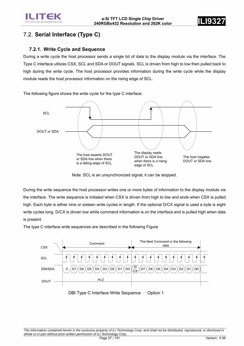
a-Si TFT LCD Single Chip Driver
240RGBx432 Resolution and 262K color ILI9327
The information contained herein is the exclusive property of ILI Technology Corp. and shall not be distributed, reproduced, or disclosed in whole or in part without prior written permission of ILI Technology Corp. Page 27 / 191 Version: 0.06
7.2. Serial Interface (Type C)
7.2.1. Write Cycle and Sequence During a write cycle the host processor sends a single bit of data to the display module via the interface. The
Type C interface utilizes CSX, SCL and SDA or DOUT signals. SCL is driven from high to low then pulled back to
high during the write cycle. The host processor provides information during the write cycle while the display
module reads the host processor information on the rising edge of SCL.
The following figure shows the write cycle for the type C interface.
SCL
DOUT or SDA
The host asserts DOUT or SDA line when there is a falling edge of SCL
The display reads DOUT or SDA line when there is a rising edge of SCL
The host negates DOUT or SDA line
Note: SCL is an unsynchronized signal; it can be stopped.
During the write sequence the host processor writes one or more bytes of information to the display module via
the interface. The write sequence is initiated when CSX is driven from high to low and ends when CSX is pulled
high. Each byte is either nine or sixteen write cycles in length. If the optional D/CX signal is used a byte is eight
write cycles long. D/CX is driven low while command information is on the interface and is pulled high when data
is present.
The type C interface write sequences are described in the following Figure
0 D7 D6 D5 D4 D3 D2 D1 D0 D/CX D7 D6 D5 D4 D3 D2 D1 D0
CSX
SCL
DIN/SDA
DOUT Hi-Z
Command The Next Command or the following data
DBI Type C Interface Write Sequence – Option 1

a-Si TFT LCD Single Chip Driver
240RGBx432 Resolution and 262K color ILI9327
The information contained herein is the exclusive property of ILI Technology Corp. and shall not be distributed, reproduced, or disclosed in whole or in part without prior written permission of ILI Technology Corp. Page 28 / 191 Version: 0.06
D7 D6 D5 D4 D3 D2 D1 D0 D7 D6 D5 D4 D3 D2 D1 D0
CSX
SCL
DIN/SDA
DOUT Hi-Z
Command The Next Command or the following data
DBI Type C Interface Write Sequence – Option 3
D/CX
Note:
1. D7 is MSB and D0 is LSB of byte.
2. When the Interface control register (C6h) SDA_EN is set as ‘1’, the DIN/SDA pin is bi-direction and DOUT pin is not
used.
3. When the Interface control register (C6h) SDA_EN is set as ‘0’, the DIN/SDA pin is uni-direction and DIN and DOUT pins
are used for data write and read.
R[1]r[1]
DB7 DB6 DB5 DB4 DB3 DB2 DB1 DB0R1[0] G1[0] B1[0]
DFM01
Set_pixel_format
3'h13bpp Frame Memory Write
DBI Type C Interface IM[2:0]=101/111
R[3] R[2] R[0]R[3] r[2] r[0]
**
3'h618bpp Frame Memory Read
R[4]r[4]
R[5]r[5]
G[5] G[4] G[3] G[2] G[1] G[0]g[5] g[4] g[3] g[2] g[1] g[0]
B[4] B[3] B[2] B[1] B[0]b[3] b[2] b[1] b[0]b[4]
B[5]b[5]
18bpp Frame Memory Write
R2[0] G2[0] B2[0]R2[0] G2[0] B2[0]
DB7 DB6 DB5 DB4 DB3 DB2 DB1 DB0R3[0] G3[0] B3[0] R4[0] G4[0] B4[0]
DB7 DB6 DB5 DB4 DB3 DB2 DB1 DB0R5[0] G5[0] B5[0] R6[0] G6[0] B6[0]
DB17 DB16 DB15 DB14 DB13 DB12 DB11 DB10 DB9 DB8 DB7 DB6 DB5 DB4 DB3 DB2 DB1 DB0R[5] R[4] R[3] R[2] R[1] R[0] G[5] G[4] G[3] G[2] G[1] G[0] B[5] B[4] B[3] B[2] B[1] B[0]
EPF[1:0]**
Set_pixel_format18bpp3bpp G[0]R[0] B[0]
Frame Memory Data (18bpp)
3/16-bit data extend to 18-bit
R[0]R[0]R[0]R[0]R[0] R[0] G[0]G[0]G[0]G[0]G[0] B[0]B[0]B[0]B[0]B[0]
G1[0]R1[0] B1[0] R3[0] B3[0]G3[0] R4[0] G4[0] B4[0] R5[0] G5[0] B5[0] R6[0] G6[0] B6[0]
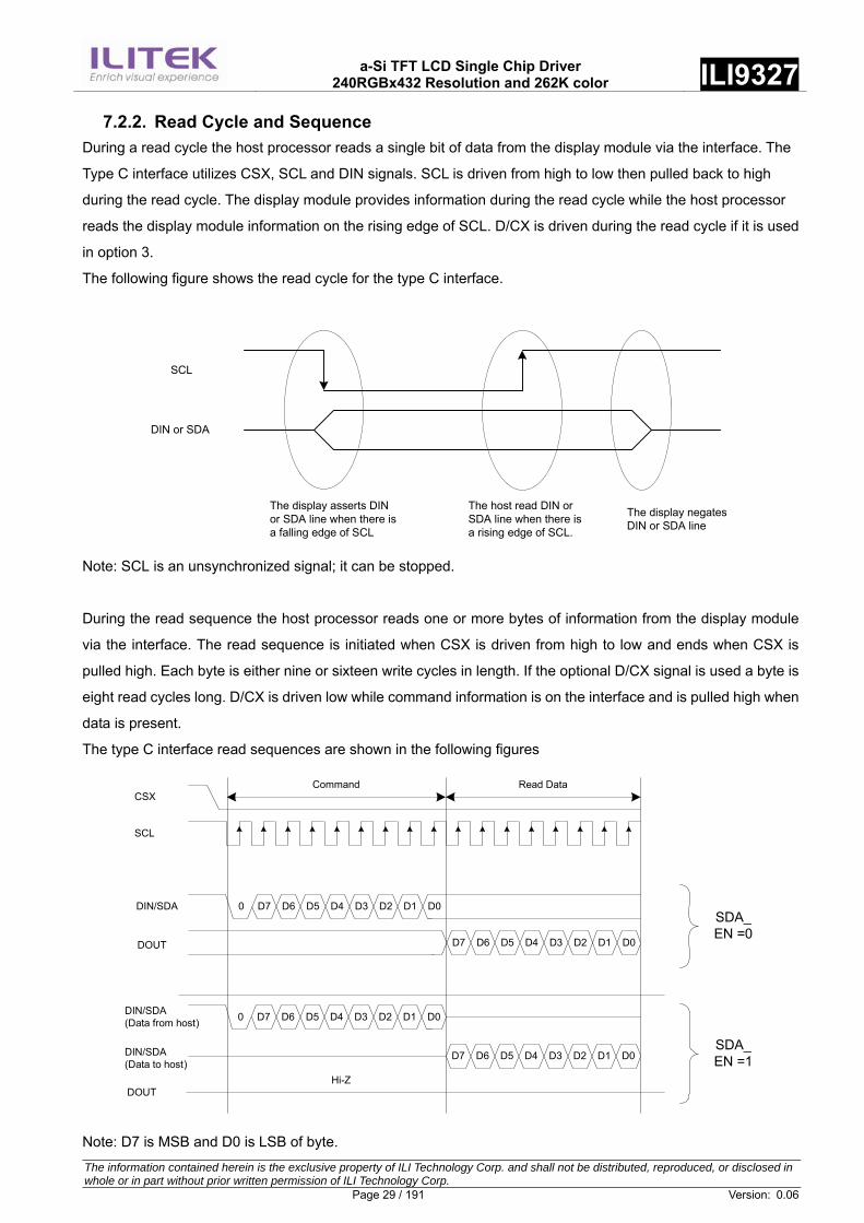
a-Si TFT LCD Single Chip Driver
240RGBx432 Resolution and 262K color ILI9327
The information contained herein is the exclusive property of ILI Technology Corp. and shall not be distributed, reproduced, or disclosed in whole or in part without prior written permission of ILI Technology Corp. Page 29 / 191 Version: 0.06
7.2.2. Read Cycle and Sequence During a read cycle the host processor reads a single bit of data from the display module via the interface. The
Type C interface utilizes CSX, SCL and DIN signals. SCL is driven from high to low then pulled back to high
during the read cycle. The display module provides information during the read cycle while the host processor
reads the display module information on the rising edge of SCL. D/CX is driven during the read cycle if it is used
in option 3.
The following figure shows the read cycle for the type C interface.
SCL
DIN or SDA
The display asserts DIN or SDA line when there is a falling edge of SCL
The host read DIN or SDA line when there is a rising edge of SCL.
The display negates DIN or SDA line
Note: SCL is an unsynchronized signal; it can be stopped.
During the read sequence the host processor reads one or more bytes of information from the display module
via the interface. The read sequence is initiated when CSX is driven from high to low and ends when CSX is
pulled high. Each byte is either nine or sixteen write cycles in length. If the optional D/CX signal is used a byte is
eight read cycles long. D/CX is driven low while command information is on the interface and is pulled high when
data is present.
The type C interface read sequences are shown in the following figures
0 D7 D6 D5 D4 D3 D2 D1 D0
CSX
SCL
DIN/SDA
DOUT
Command Read Data
D7 D6 D5 D4 D3 D2 D1 D0
0 D7 D6 D5 D4 D3 D2 D1 D0DIN/SDA(Data from host)
DIN/SDA(Data to host)
D7 D6 D5 D4 D3 D2 D1 D0SDA_EN =1
SDA_EN =0
DOUTHi-Z
Note: D7 is MSB and D0 is LSB of byte.

a-Si TFT LCD Single Chip Driver
240RGBx432 Resolution and 262K color ILI9327
The information contained herein is the exclusive property of ILI Technology Corp. and shall not be distributed, reproduced, or disclosed in whole or in part without prior written permission of ILI Technology Corp. Page 30 / 191 Version: 0.06
D7 D6 D5 D4 D3 D2 D1 D0
CSX
SCL
DIN/SDA
DOUT
Command Read Data
D7 D6 D5 D4 D3 D2 D1 D0
D7 D6 D5 D4 D3 D2 D1 D0DIN/SDA(Data from host)
DIN/SDA(Data to host)
D7 D6 D5 D4 D3 D2 D1 D0SDA_EN =1
SDA_EN =0
DOUTHi-Z
D/CX
7.2.3. Break and Pause Sequences The host processor can break a read or write sequence by pulling the CSX signal high during a command or
data byte. The display module shall reset its interface so it will be ready to receive the same byte when CSX is
again driven low.
The host processor can pause a read or write sequence by pulling the CSX signal high between command or
data bytes. The display module shall wait for the host processor to drive CSX low before continuing the read or
write sequence at the point where the sequence was paused.

a-Si TFT LCD Single Chip Driver
240RGBx432 Resolution and 262K color ILI9327
The information contained herein is the exclusive property of ILI Technology Corp. and shall not be distributed, reproduced, or disclosed in whole or in part without prior written permission of ILI Technology Corp. Page 31 / 191 Version: 0.06
Break can be e.g. another command or noise pulse.

a-Si TFT LCD Single Chip Driver
240RGBx432 Resolution and 262K color ILI9327
The information contained herein is the exclusive property of ILI Technology Corp. and shall not be distributed, reproduced, or disclosed in whole or in part without prior written permission of ILI Technology Corp. Page 32 / 191 Version: 0.06
7.3. Display Pixel Interface (DPI) In normal operation, systems based on DPI architecture rely on the host processor to continuously provide
complete frames of image data at a sufficient frame rate to avoid flicker or other visible artifacts. The displayed
image, or frame, is comprised of a rectangular array of pixels. The frame is transmitted from the host processor
to a display module as a sequence of pixels, with each horizontal line of the image data sent as a group of
consecutive pixels.
Vsync indicates the beginning of each frame of the displayed image.
Hsync signals the beginning of each horizontal line of pixels.
Each pixel value (16 or 18-bit data) is transferred from the host processor to the display module during one pixel
period. The rising edge of PCLK is used by the display module to capture pixel data. Since PCLK runs
continuously, control signal DE is required to indicate when valid pixel data is being transmitted on the pixel data
signals.
VSYNC
HSYNC
DOTCLK
Moving picture display area
ENABLE
RAM data display area
Back porch period
Display period
Front porch period
DB[17:0]
Note 1: Front porch period continues until the next input of VSYNC.
Note 2: Input DOTCLK throughout the operation.
Note 3: Supply the VSYNC, HSYNC and DOTCLK with frequency that can meet the resolution requirement of panel.

a-Si TFT LCD Single Chip Driver
240RGBx432 Resolution and 262K color ILI9327
The information contained herein is the exclusive property of ILI Technology Corp. and shall not be distributed, reproduced, or disclosed in whole or in part without prior written permission of ILI Technology Corp. Page 33 / 191 Version: 0.06
Hsync HBP HAdr HFP
Vsy
ncVA
drVF
P
(VAdr + HAdr) - Periodwhen valid display data aretransferred from host todisplay module
(Vsync + VBP) - V
ertical interval when no valid
display data is transferred from host to display
(Hsync + HBP) – Horizontal interval when novalid display data is sent from host to display
VFP -- Vertical interval when no valid displaydata is transferred from host to display
HFP - H
orizontal interval when no valid
display data is sent from host to display
VBP
Parameters Symbols Condition Min. Typ. Max. Units
PCLK Cycle PCLKCYC - 88 - ns Horizontal Synchronization Hsync - 10 - PCLK Horizontal Back Porch HBP - 20 - PCLK Horizontal Address HAdr - 320 - PCLK Horizontal Front Porch HFP - 10 - PCLK Vertical Synchronization Vsync - 2 - Line Vertical Back Porch VBP - 2 - Line Vertical Address VAdr - 432 - Line Vertical Front Porch VFP - 4 - Line Vsync setup time VSST - Hz Vsync hold time VSHT - Hz Hsync setup time HSST - Hz Hsync hold time HSHT - Hz Data setup time DST - Hz Data hold time DHT - Hz Vertical Frequency(*) 60 - Hz Horizontal Frequency(*) - 29.282 - KHz PCLK Frequency(*) - 11.42Mhz TBD MHz
Notes:
1. Vertical period (one frame) shall be equal to the sum of Vsync + VBP + VAdr + VFP.
2. Horizontal period (one line) shall be equal to the sum of Hsync + HBP + HAdr + HFP.
3. Control signals PCLK and Hsync shall be transmitted as specified at all times while valid pixels are transferred
between the host processor and the display module.

a-Si TFT LCD Single Chip Driver
240RGBx432 Resolution and 262K color ILI9327
The information contained herein is the exclusive property of ILI Technology Corp. and shall not be distributed, reproduced, or disclosed in whole or in part without prior written permission of ILI Technology Corp. Page 34 / 191 Version: 0.06
DB17 DB16 DB15 DB14 DB13 DB12 DB11 DB10 DB9 DB8 DB7 DB6 DB5 DB4 DB3 DB2 DB1 DB0
R[5] R[4] R[3] R[2] R[1] R[0] G[5] G[4] G[3] G[2] G[1] G[0] B[5] B[4] B[3] B[2] B[1] B[0]
DPI (RGB) Interface
18bit DPI Interface Connection: set_pixel_format D[6:4]=3'h6:18bpp
16bit DPI Interface Connection: set_pixel_format D[6:4]=3'h5:16bpp
DB17 DB16 DB15 DB14 DB13 DB12 DB11 DB10 DB9 DB8 DB7 DB6 DB5 DB4 DB3 DB2 DB1 DB0
R[4] R[3] R[2] R[1] R[0] G[5] G[4] G[3] G[2] G[1] G[0] B[4] B[3] B[2] B[1] B[0]
DPI (RGB) Interface
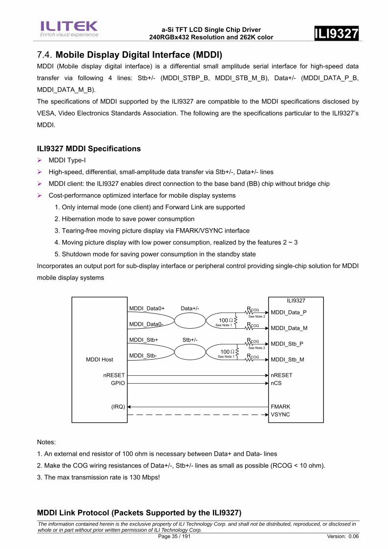
a-Si TFT LCD Single Chip Driver
240RGBx432 Resolution and 262K color ILI9327
The information contained herein is the exclusive property of ILI Technology Corp. and shall not be distributed, reproduced, or disclosed in whole or in part without prior written permission of ILI Technology Corp. Page 35 / 191 Version: 0.06
7.4. Mobile Display Digital Interface (MDDI) MDDI (Mobile display digital interface) is a differential small amplitude serial interface for high-speed data
transfer via following 4 lines: Stb+/- (MDDI_STBP_B, MDDI_STB_M_B), Data+/- (MDDI_DATA_P_B,
MDDI_DATA_M_B).
The specifications of MDDI supported by the ILI9327 are compatible to the MDDI specifications disclosed by
VESA, Video Electronics Standards Association. The following are the specifications particular to the ILI9327’s
MDDI.
ILI9327 MDDI Specifications MDDI Type-I
High-speed, differential, small-amplitude data transfer via Stb+/-, Data+/- lines
MDDI client: the ILI9327 enables direct connection to the base band (BB) chip without bridge chip
Cost-performance optimized interface for mobile display systems
1. Only internal mode (one client) and Forward Link are supported
2. Hibernation mode to save power consumption
3. Tearing-free moving picture display via FMARK/VSYNC interface
4. Moving picture display with low power consumption, realized by the features 2 ~ 3
5. Shutdown mode for saving power consumption in the standby state
Incorporates an output port for sub-display interface or peripheral control providing single-chip solution for MDDI
mobile display systems
MDDI Host
MDDI_Data0+
MDDI_Data0-
MDDI_Stb+
MDDI_Stb-
ILI9327
MDDI_Data_P
MDDI_Stb_P
MDDI_Data_M
MDDI_Stb_M
nRESETnCS
FMARKVSYNC
nRESETGPIO
(IRQ)
Data+/-
Stb+/-
100Ω
RCOG
RCOG
RCOG
RCOG
See Note 2
See Note 2
See Note 1
100ΩSee Note 1
Notes:
1. An external end resistor of 100 ohm is necessary between Data+ and Data- lines
2. Make the COG wiring resistances of Data+/-, Stb+/- lines as small as possible (RCOG < 10 ohm).
3. The max transmission rate is 130 Mbps!
MDDI Link Protocol (Packets Supported by the ILI9327)

a-Si TFT LCD Single Chip Driver
240RGBx432 Resolution and 262K color ILI9327
The information contained herein is the exclusive property of ILI Technology Corp. and shall not be distributed, reproduced, or disclosed in whole or in part without prior written permission of ILI Technology Corp. Page 36 / 191 Version: 0.06
The MDDI Link Protocol of the ILI9327 is in line with the MDDI specifications disclosed by VESA. See the MDDI
specifications by VESA for details on the MDDI Link Protocol.
The MDDI packets supported by the ILI9327 are as follows. Do not send packets not supported by the ILI9327 in
the system incorporating the ILI9327.
Refer to MDDI packet structure, sub-frame header packet is placed in front of a sub-frame and some sub-frame
construct media-frame together. The following table describes 9 types of packet which is supported in ILI9327.
Packet Function Direction
Sub-frame header packet Header of each sub frame Forward Register access packet Register setting Forward Video stream packet Video data transfer Forward Filler packet Fill empty packet space Forward Reverse link encapsulation packet Reverse data packet Reverse Round-trip delay measurement packet Host->client->host delay check Forward/ReverseClient capability packet Capability of client check Reverse Client request and status packet Information about client status Reverse Link shutdown packet End of frame Forward

a-Si TFT LCD Single Chip Driver
240RGBx432 Resolution and 262K color ILI9327
The information contained herein is the exclusive property of ILI Technology Corp. and shall not be distributed, reproduced, or disclosed in whole or in part without prior written permission of ILI Technology Corp. Page 37 / 191 Version: 0.06
Sub-Frame Header Packet 0 1 2 3 4 5 6 7
1 Packet Length 2 (0x0014) 3 Packet Type 4 (0x3bFF) 5 Unique Word 6 (0x005A) 7 Reserved 1 8 (0x0000) 9 Sub-Frame Length 10 11 12 13 Protocol Version 14 (0x0000) 15 Sub-frame Count 16 17 Media-frame Count 18 19 20 21 CRC 22 (0x0000)
Bytes

a-Si TFT LCD Single Chip Driver
240RGBx432 Resolution and 262K color ILI9327
The information contained herein is the exclusive property of ILI Technology Corp. and shall not be distributed, reproduced, or disclosed in whole or in part without prior written permission of ILI Technology Corp. Page 38 / 191 Version: 0.06
Video Stream Packet The ILI9327 writes image data to RAM via Video Stream Packet. The window and RAM addresses are set via
Register Access Packet.
PacketLength
PacketType = 16 bClient ID
Video Data format
Descriptor2 Bytes 2 Bytes 2 Bytes 2 Bytes
Pixel Data Attributes
2 Bytes
X Left Edge
2 Bytes
Y Top Edge
2 Bytes
X RightEdge
2 Bytes
Y BottomEdge
2 Bytes
X Start
2 Bytes
Y Start
2 Bytes
Pixel Count
2 Bytes
Parameter CRC
2 Bytes
Pixel Data
Packet Length - 26Bytes
Pixel Data CRC
2 Bytes
0 1 2 3 4 5 6 7 1 Packet Length 2 3 Packet Type 4 (0x0010) 5 bClient ID 6 (0x0000) 7 Video Data Format Descriptor 8 9 Bit0 Bit1 Pixel Data Attributes 10 11 X Left Edge 12 13 Y Top Edge 14 15 X Right Edge 16 17 Y Bottom Edge 18 19 X Start 20 21 Y Start 22 23 Pixel Count 24 25 Parameter CRC 26
Pixel Data (Packet Length - 26 bytes)
CRC
Note: The parameters colored in gray are not supported by the ILI9327.

a-Si TFT LCD Single Chip Driver
240RGBx432 Resolution and 262K color ILI9327
The information contained herein is the exclusive property of ILI Technology Corp. and shall not be distributed, reproduced, or disclosed in whole or in part without prior written permission of ILI Technology Corp. Page 39 / 191 Version: 0.06
Video Data Format Descriptor: sets the pixel data format. The ILI9327 supports only the following format. Set
the same pixel format (bpp) as selected by DSS[1:0] in Video Data Format Descriptor.
[15:13] [12] [11:8] [7:4] [3:0]
010 1 0x5 0x6 0x5 Packed 16bpp RGB format (R:G:B=5:6:5)
010 1 0x6 0x6 0x6 Packed 18bpp RGB format (R:G:B=6:6:6)
Others Setting disabled
MDDI Bytes n MDDI Bytes (n+1) MDDI Bytes (n+2) 0 1 2 3 4 5 6 7 0 1 2 3 4 5 6 7 0 1 2 3 4 5 6 7
Packet 16bpp
0 1 2 3 4 0 1 2 3 4 5 0 1 2 3 4 0 1 2 3 4 0 1 2Pixel 1 Blue Pixel 1 Green Pixel 1 Red Pixel 2 Blue Pixel 2
Packet 18bpp
0 1 2 3 4 5 0 1 2 3 4 5 0 1 2 3 4 5 0 1 2 3 4 5Pixel 2 Blue Pixel 2 Green Pixel 2 Red Pixel 2 Blue
Pixel Data Attributes: the image data sent vial Video Stream Packet is recognized as either the data for the
main-panel or for the sub-panel according to the setting in [1:0] bits in this field.
Pixel Data Attributes
Bits[1:0] Description
0x0000 00 The Video Stream Packet data is recognized as the sub-panel data. The Video Stream Packet data is
outputted via sub-display interface and not written in the ILI9327.
0x0001 01 Setting disabled 0x0002 10 Setting disabled 0x0003 11 The Video Stream Packet data is recognized as the data written in the ILI9327. The Video Stream Packet
data is written in the ILI9327 and not outputted via sub-display interface. Others
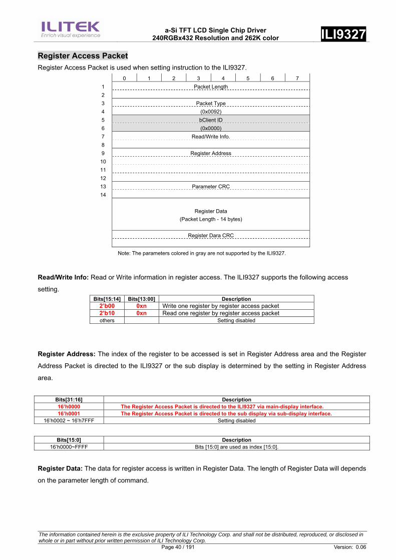
a-Si TFT LCD Single Chip Driver
240RGBx432 Resolution and 262K color ILI9327
The information contained herein is the exclusive property of ILI Technology Corp. and shall not be distributed, reproduced, or disclosed in whole or in part without prior written permission of ILI Technology Corp. Page 40 / 191 Version: 0.06
Register Access Packet Register Access Packet is used when setting instruction to the ILI9327.
0 1 2 3 4 5 6 7 1 Packet Length 2 3 Packet Type 4 (0x0092) 5 bClient ID 6 (0x0000) 7 Read/Write Info. 8 9 Register Address 10 11 12 13 Parameter CRC 14
Register Data (Packet Length - 14 bytes)
Register Dara CRC
Note: The parameters colored in gray are not supported by the ILI9327.
Read/Write Info: Read or Write information in register access. The ILI9327 supports the following access
setting. Bits[15:14] Bits[13:00] Description
2’b00 0xn Write one register by register access packet 2’b10 0xn Read one register by register access packet others Setting disabled
Register Address: The index of the register to be accessed is set in Register Address area and the Register
Address Packet is directed to the ILI9327 or the sub display is determined by the setting in Register Address
area.
Bits[31:16] Description 16’h0000 The Register Access Packet is directed to the ILI9327 via main-display interface. 16’h0001 The Register Access Packet is directed to the sub display via sub-display interface.
16’h0002 ~ 16’h7FFF Setting disabled
Bits[15:0] Description
16’h0000~FFFF Bits [15:0] are used as index [15:0].
Register Data: The data for register access is written in Register Data. The length of Register Data will depends
on the parameter length of command.

a-Si TFT LCD Single Chip Driver
240RGBx432 Resolution and 262K color ILI9327
The information contained herein is the exclusive property of ILI Technology Corp. and shall not be distributed, reproduced, or disclosed in whole or in part without prior written permission of ILI Technology Corp. Page 41 / 191 Version: 0.06
Example of Register Access Packet (e.g. write to the ILI9327) 0 1 2 3 4 5 6 7
1 Packet Length (0x12) 2 (0x00) 3 Packet Type (0x92) 4 (0x00) 5 bClient ID (0x00) 6 (0x00) 7 Read/Write Info. (0x01) 8 (0x00) 9 Register Address (index ID[7:0]) 10 (index ID[15:8])
11 (0x00) Main Panel (ILI9327)
(0x01) Sub panel 12 (0x00) 13 Parameter CRC 14 15 Register Data List (Various Length) 1st Parameter 16 2nd Parameter 17 3rd Parameter 18 0x00 19 Parameter CRC 20
Note: The parameters colored in gray are not supported by the ILI9327.

a-Si TFT LCD Single Chip Driver
240RGBx432 Resolution and 262K color ILI9327
The information contained herein is the exclusive property of ILI Technology Corp. and shall not be distributed, reproduced, or disclosed in whole or in part without prior written permission of ILI Technology Corp. Page 42 / 191 Version: 0.06
Register Access Packet Restrictions
The ILI9327’s internal RAM is accessible via Video Stream Packet. RAM access data is not included in Register
Access Packet.
Link Shutdown Packet
This packet is used to bring Link to the Hibernation state. 0 1 2 3 4 5 6 7
1 Packet Length 2 (0X0014) 3 Packet Type 4 (0x0045) 5 Parameter CRC 6 7
All Zeros
(Type-I: 16 bytes)
22
Note: The parameters colored in gray are not supported by the ILI9327.
Filler Packet 0 1 2 3 4 5 6 7
1 Packet Length 2 3 Packet Type 4 (0x0000)
Filler bytes (all zeros) (Packet Length: 4 bytes)
CRC
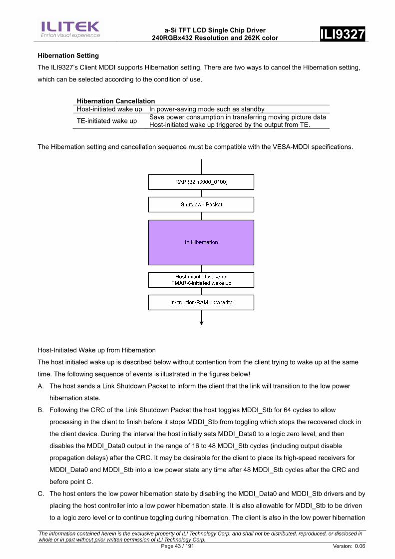
a-Si TFT LCD Single Chip Driver
240RGBx432 Resolution and 262K color ILI9327
The information contained herein is the exclusive property of ILI Technology Corp. and shall not be distributed, reproduced, or disclosed in whole or in part without prior written permission of ILI Technology Corp. Page 43 / 191 Version: 0.06
Hibernation Setting
The ILI9327’s Client MDDI supports Hibernation setting. There are two ways to cancel the Hibernation setting,
which can be selected according to the condition of use.
Hibernation Cancellation Host-initiated wake up In power-saving mode such as standby
TE-initiated wake up Save power consumption in transferring moving picture data Host-initiated wake up triggered by the output from TE.
The Hibernation setting and cancellation sequence must be compatible with the VESA-MDDI specifications.
Host-Initiated Wake up from Hibernation
The host initialed wake up is described below without contention from the client trying to wake up at the same
time. The following sequence of events is illustrated in the figures below!
A. The host sends a Link Shutdown Packet to inform the client that the link will transition to the low power
hibernation state.
B. Following the CRC of the Link Shutdown Packet the host toggles MDDI_Stb for 64 cycles to allow
processing in the client to finish before it stops MDDI_Stb from toggling which stops the recovered clock in
the client device. During the interval the host initially sets MDDI_Data0 to a logic zero level, and then
disables the MDDI_Data0 output in the range of 16 to 48 MDDI_Stb cycles (including output disable
propagation delays) after the CRC. It may be desirable for the client to place its high-speed receivers for
MDDI_Data0 and MDDI_Stb into a low power state any time after 48 MDDI_Stb cycles after the CRC and
before point C.
C. The host enters the low power hibernation state by disabling the MDDI_Data0 and MDDI_Stb drivers and by
placing the host controller into a low power hibernation state. It is also allowable for MDDI_Stb to be driven
to a logic zero level or to continue toggling during hibernation. The client is also in the low power hibernation
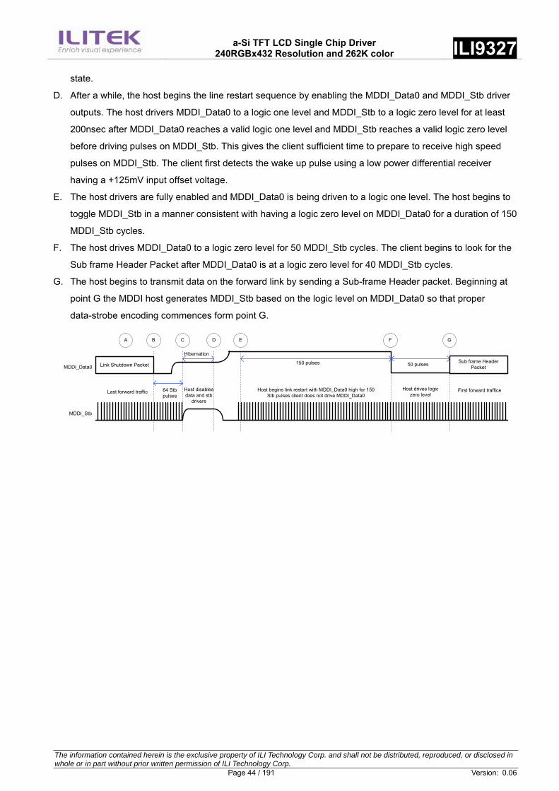
a-Si TFT LCD Single Chip Driver
240RGBx432 Resolution and 262K color ILI9327
The information contained herein is the exclusive property of ILI Technology Corp. and shall not be distributed, reproduced, or disclosed in whole or in part without prior written permission of ILI Technology Corp. Page 44 / 191 Version: 0.06
state.
D. After a while, the host begins the line restart sequence by enabling the MDDI_Data0 and MDDI_Stb driver
outputs. The host drivers MDDI_Data0 to a logic one level and MDDI_Stb to a logic zero level for at least
200nsec after MDDI_Data0 reaches a valid logic one level and MDDI_Stb reaches a valid logic zero level
before driving pulses on MDDI_Stb. This gives the client sufficient time to prepare to receive high speed
pulses on MDDI_Stb. The client first detects the wake up pulse using a low power differential receiver
having a +125mV input offset voltage.
E. The host drivers are fully enabled and MDDI_Data0 is being driven to a logic one level. The host begins to
toggle MDDI_Stb in a manner consistent with having a logic zero level on MDDI_Data0 for a duration of 150
MDDI_Stb cycles.
F. The host drives MDDI_Data0 to a logic zero level for 50 MDDI_Stb cycles. The client begins to look for the
Sub frame Header Packet after MDDI_Data0 is at a logic zero level for 40 MDDI_Stb cycles.
G. The host begins to transmit data on the forward link by sending a Sub-frame Header packet. Beginning at
point G the MDDI host generates MDDI_Stb based on the logic level on MDDI_Data0 so that proper
data-strobe encoding commences form point G.
Link Shutdown PacketSub frame Header
Packet
MDDI_Stb
MDDI_Data0
Hibernation
150 pulses 50 pulses
64 Stb pulses
Last forward traffic Host disables data and stb
drivers
Host begins link restart with MDDI_Data0 high for 150 Stb pulses client does not drive MDDI_Data0
Host drives logic zero level
First forward traffice
A B C D E F G

a-Si TFT LCD Single Chip Driver
240RGBx432 Resolution and 262K color ILI9327
The information contained herein is the exclusive property of ILI Technology Corp. and shall not be distributed, reproduced, or disclosed in whole or in part without prior written permission of ILI Technology Corp. Page 45 / 191 Version: 0.06
8. Command
8.1. Command List Operational Code (Hex)
Command Command(C)
/Read(R) /Write(W)Number Of Parameter
MIPI DCS Type1 Requirement
ILI9327 Implementation
00h nop C 0 Yes Yes 01h soft_reset C 0 Yes Yes 06h get_red_channel R 1 No No 07h get_green_channel R 1 No No 08h get_blue_channel R 1 No No 0Ah get_power_mode R 1 Yes Yes
0Bh get_address_mode R 1 Yes (Bit[7:0]) Yes (Bit[7:3]) ,
Only) 0Ch get_pixel_format R 1 Yes Yes 0Dh get_display_mode R 1 Yes Yes 0Eh get_signal_mode R 1 Yes Yes
0Fh get_diagnostic _result R 1 Bit7/6:Yes
Bit5/4:Optional Yes (Bit7/6 Only)
10h enter_sleep_mode C 0 Yes Yes 11h exit_sleep_mode C 0 Yes Yes 12h enter_partial_mode C 0 Yes Yes 13h enter_normal_mode C 0 Yes Yes 20h exit_invert_mode C 0 Yes Yes 21h enter_invert_mode C 0 Yes Yes 28h set_display_off C 0 Yes Yes 29h set_display_on C 0 Yes Yes 2Ah set_column_address W 4 Yes Yes 2Bh set_page_address W 4 Yes Yes 2Ch write_memory_start W Variable Yes Yes 2Eh read_memory_start R Variable Yes Yes 30h set_partial_area W 4 Yes Yes 33h set_scroll_area W 6 Yes Yes 34h set_tear_off C 0 Yes Yes 35h set_tear_on W 1 Yes Yes
36h set_address_mode W 1 Yes (Bit7-0) Yes (Bit[7:3], Bit[1:0] Only)
37h set_scroll_start W 2 Yes Yes 38h exit_idle_mode C 0 Yes Yes 39h enter_idle_mode C 0 Yes Yes 3Ah set_pixel_format W 1 Yes Yes 3Ch write_memory _continue W Variable Yes Yes 3Eh read_memory _continue R Variable Yes Yes 44h set_tear_scanline W 2 Yes Yes 45h get_scanline R 2 Yes Yes 51h Write Display Brightness W 1 - Yes 52h Read Display Brightness R 1 - Yes 53h Write CTRL Display W 1 - Yes 54h Read CTRL Display R 1 - Yes
55h Write Content Adaptive Brightness Control
W 1 - Yes
56h Read Content Adaptive Brightness Control
R 1 - Yes
5Eh Write CABC Minimum Brightness W 1 - Yes 5Fh Read CABC Minimum Brightness R 1 - Yes

a-Si TFT LCD Single Chip Driver
240RGBx432 Resolution and 262K color ILI9327
The information contained herein is the exclusive property of ILI Technology Corp. and shall not be distributed, reproduced, or disclosed in whole or in part without prior written permission of ILI Technology Corp. Page 46 / 191 Version: 0.06
A1h read_DDB_start R 1 Yes Yes B0h Command Access Protect R/W 1 - Yes B1h Low Power Mode Control R/W 1 - Yes
B3h Frame Memory Access and Interface Setting
R/W 4 - Yes
B4h Display Mode and Frame Memory Write Mode Setting
R/W 1 - Yes
B5h Sub-Panel Control Register R/W 1 - Yes B8h Backlight Control 1 R/W 1 - Yes B9h Backlight Control 2 R/W 1 - Yes BAh Backlight Control 3 R/W 1 - Yes BBh Backlight Control 4 R/W 1 - Yes BCh Backlight Control 5 R/W 1 - Yes BEh Backlight Control 7 R/W 1 - Yes BFh Backlight Control 8 R/W 1 - Yes C0h Panel Driving Setting R/W 6 Yes
C1h Display_Timing_Setting for Normal/Partial Mode
R/W Yes
C3h Display_Timing_Setting for Idle Mode
R/W Yes
C4h Source/VCOM/Gate Timing Setting R/W Yes C5h Frame Rate Control R/W Yes C6h Interface Control R/W Yes C8h Gamma Setting R/W Yes C9h Gamma Setting for Red/Blue Color R/W Yes D0h Power_Setting R/W Yes D1h VCOM Control R/W Yes D2h Power_Setting for Normal Mode R/W Yes D3h Power_Setting for Partial Mode R/W Yes D4h Power_Setting for Idle Mode R/W Yes E0h NV Memory Write R/W Yes E1h NV Memory Control R/W Yes E2h NV Memory Status Read R/W Yes E3h NV Memory Protection R/W Yes EAh 3-Gamma Function Control R/W Yes EFh Device Code Read R/W Yes

a-Si TFT LCD Single Chip Driver
240RGBx432 Resolution and 262K color ILI9327
The information contained herein is the exclusive property of ILI Technology Corp. and shall not be distributed, reproduced, or disclosed in whole or in part without prior written permission of ILI Technology Corp. Page 47 / 191 Version: 0.06
Operational Code (Hex) Function Command(C)
Read(R)/Write(W) Number Of Parameter
B0h Command Access Protect W/R 1 B1h Low Power Mode Control W/R 1 B3h Frame Memory Access and Interface setting W/R 5
B4h Display Mode and Frame Memory Write Mode setting
W/R 1
BFh Device code Read R 4 C0h Panel Driving Setting W/R 7 C1h Display Timing Setting for Normal Mode W/R 3 C2h Display Timing Setting for Partial Mode W/R 3 C3h Display Timing Setting for Idle Mode W/R 3 C5h Frame rate and Inversion Control W/R 1 C6h Interface Control W/R 1 C8h Gamma Setting W/R 12 D0h Power Setting W/R 3 D1h VCOM Control W/R 3 D2h Power Setting for Normal Mode W/R 2 D3h Power Setting for Partial Mode W/R 2 D4h Power Setting for Idle Mode W/R 2 E0h NV Memory Write W/R 1 E1h NV Memory Control W/R 1 E2h NV Memory Status W/R 3 E3h NV Memory Protection W/R 2
B0~FF Except above command
LSI TEST Registers W/R Variable

a-Si TFT LCD Single Chip Driver
240RGBx432 Resolution and 262K color ILI9327
The information contained herein is the exclusive property of ILI Technology Corp. and shall not be distributed, reproduced, or disclosed in whole or in part without prior written permission of ILI Technology Corp. Page 48 / 191 Version: 0.06
8.2. Command Description
8.2.1. NOP (00h) 00H NOP (No Operation)
D/CX RDX WRX D17-D8 D7 D6 D5 D4 D3 D2 D1 D0 HEX
Command 0 1 ↑ X 0 0 0 0 0 0 0 0 00
Parameter NO PARAMETER
Description
This command is an empty command; it does not have any effect on the display module. However it can be used to terminate
Frame Memory Write or Read as described in RAMWR (Memory Write) and RAMRD (Memory Read) Commands.
X = Don’t care.
Restriction None
Register
Availability
Status Availability
Normal Mode On, Idle Mode Off, Sleep Out Yes
Normal Mode On, Idle Mode On, Sleep Out Yes
Partial Mode On, Idle Mode Off, Sleep Out Yes
Partial Mode On, Idle Mode On, Sleep Out Yes
Sleep In Yes
Default
Status Default Value
Power On Sequence N/A
SW Reset N/A
HW Reset N/A
Flow Chart None
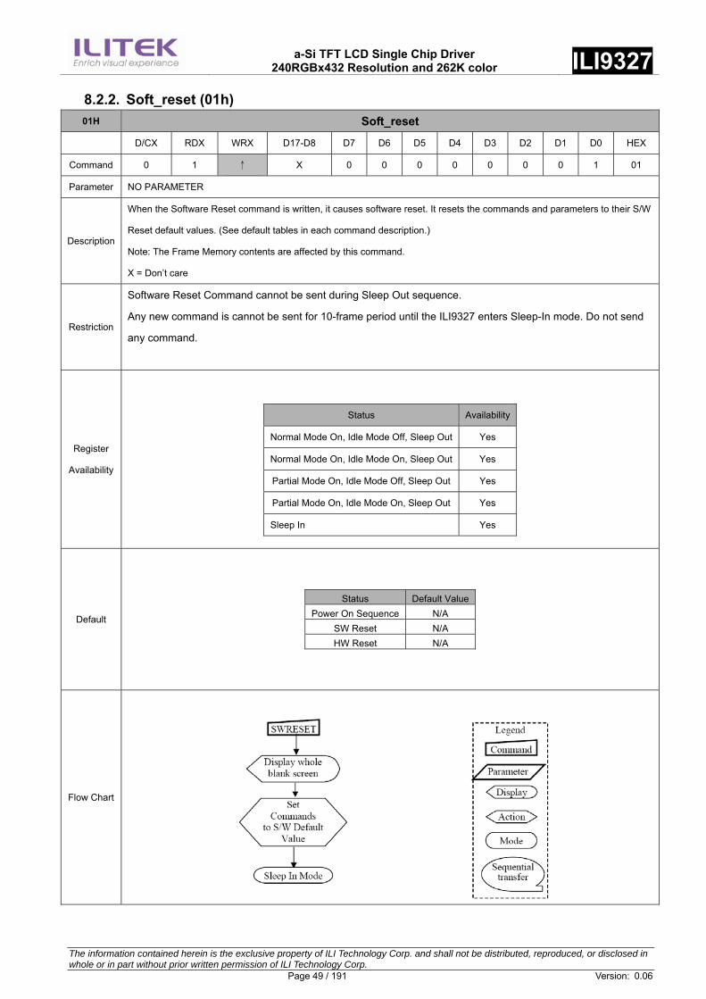
a-Si TFT LCD Single Chip Driver
240RGBx432 Resolution and 262K color ILI9327
The information contained herein is the exclusive property of ILI Technology Corp. and shall not be distributed, reproduced, or disclosed in whole or in part without prior written permission of ILI Technology Corp. Page 49 / 191 Version: 0.06
8.2.2. Soft_reset (01h) 01H Soft_reset
D/CX RDX WRX D17-D8 D7 D6 D5 D4 D3 D2 D1 D0 HEX
Command 0 1 ↑ X 0 0 0 0 0 0 0 1 01
Parameter NO PARAMETER
Description
When the Software Reset command is written, it causes software reset. It resets the commands and parameters to their S/W
Reset default values. (See default tables in each command description.)
Note: The Frame Memory contents are affected by this command.
X = Don’t care
Restriction
Software Reset Command cannot be sent during Sleep Out sequence.
Any new command is cannot be sent for 10-frame period until the ILI9327 enters Sleep-In mode. Do not send
any command.
Register
Availability
Status Availability
Normal Mode On, Idle Mode Off, Sleep Out Yes
Normal Mode On, Idle Mode On, Sleep Out Yes
Partial Mode On, Idle Mode Off, Sleep Out Yes
Partial Mode On, Idle Mode On, Sleep Out Yes
Sleep In Yes
Default
Status Default ValuePower On Sequence N/A
SW Reset N/A HW Reset N/A
Flow Chart
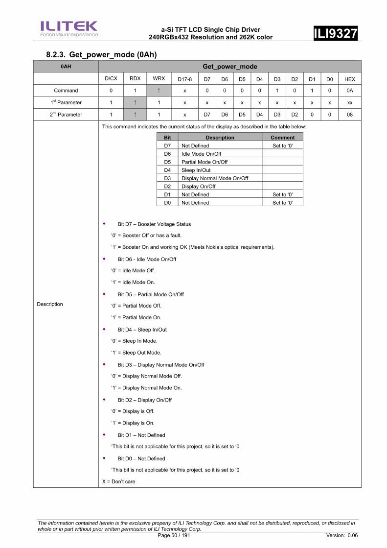
a-Si TFT LCD Single Chip Driver
240RGBx432 Resolution and 262K color ILI9327
The information contained herein is the exclusive property of ILI Technology Corp. and shall not be distributed, reproduced, or disclosed in whole or in part without prior written permission of ILI Technology Corp. Page 50 / 191 Version: 0.06
8.2.3. Get_power_mode (0Ah) 0AH Get_power_mode
D/CX RDX WRX D17-8 D7 D6 D5 D4 D3 D2 D1 D0 HEX
Command 0 1 ↑ x 0 0 0 0 1 0 1 0 0A
1st Parameter 1 ↑ 1 x x x x x x x x x xx
2nd Parameter 1 ↑ 1 x D7 D6 D5 D4 D3 D2 0 0 08
Description
This command indicates the current status of the display as described in the table below:
Bit Description Comment D7 Not Defined Set to ‘0’ D6 Idle Mode On/Off D5 Partial Mode On/Off D4 Sleep In/Out D3 Display Normal Mode On/Off D2 Display On/Off D1 Not Defined Set to ‘0’ D0 Not Defined Set to ‘0’
Bit D7 – Booster Voltage Status
‘0’ = Booster Off or has a fault.
‘1’ = Booster On and working OK (Meets Nokia’s optical requirements).
Bit D6 - Idle Mode On/Off
‘0’ = Idle Mode Off.
‘1’ = Idle Mode On.
Bit D5 – Partial Mode On/Off
‘0’ = Partial Mode Off.
‘1’ = Partial Mode On.
Bit D4 – Sleep In/Out
‘0’ = Sleep In Mode.
‘1’ = Sleep Out Mode.
Bit D3 – Display Normal Mode On/Off
‘0’ = Display Normal Mode Off.
‘1’ = Display Normal Mode On.
Bit D2 – Display On/Off
‘0’ = Display is Off.
‘1’ = Display is On.
Bit D1 – Not Defined
‘This bit is not applicable for this project, so it is set to ‘0’
Bit D0 – Not Defined
‘This bit is not applicable for this project, so it is set to ‘0’
X = Don’t care

a-Si TFT LCD Single Chip Driver
240RGBx432 Resolution and 262K color ILI9327
The information contained herein is the exclusive property of ILI Technology Corp. and shall not be distributed, reproduced, or disclosed in whole or in part without prior written permission of ILI Technology Corp. Page 51 / 191 Version: 0.06
Register Availability
Status Availability Normal Mode On, Idle Mode Off, Sleep Out Yes Normal Mode On, Idle Mode On, Sleep Out Yes Partial Mode On, Idle Mode Off, Sleep Out Yes Partial Mode On, Idle Mode On, Sleep Out Yes Sleep In Yes
Default
Status Default Value Power On Sequence 08HEX
SW Reset 08HEX
HW Reset 08HEX
Flow Chart

a-Si TFT LCD Single Chip Driver
240RGBx432 Resolution and 262K color ILI9327
The information contained herein is the exclusive property of ILI Technology Corp. and shall not be distributed, reproduced, or disclosed in whole or in part without prior written permission of ILI Technology Corp. Page 52 / 191 Version: 0.06
8.2.4. Get_address_mode (0Bh) 0BH Get_address_mode
D/CX RDX WRX D17-0 D7 D6 D5 D4 D3 D2 D1 D0 HEX
Command 0 1 ↑ x 0 0 0 0 1 0 1 1 0B
1st Parameter 1 ↑ 1 x x x x x x x x x x
2nd Parameter 1 ↑ 1 x D7 D6 D5 D4 D3 0 0 0 xx
Description
This command indicates the current status of the display as described in the table below:
Bit Description Comment D7 Page Address Order D6 Column Address Order D5 Page/Column Order D4 Line Address Order D3 RGB/BGR Order D2 Reserved Set to ‘0’ D1 Reserved Set to ‘0’ D0 Reserved Set to ‘0’
Bit D7 – Page Address Order ‘0’ = Top to Bottom ‘1’ = Bottom to Top
Bit D6 – Column Address Order ‘0’ = Left to Right ‘1’ = Right to Left
Bit D5 - Page/Column Order ‘0’ = Normal Mode ‘1’ = Reverse Mode Note: For Bits D7 to D5, also refer to Section 8.2.3 MCU to memory write/read direction.
Bit D4 – Line Address Order ‘0’ = LCD Refresh Top to Bottom ‘1’ = LCD Refresh Bottom to Top
Bit D3 – RGB/BGR Order ‘0’ = RGB ‘1’ = BGR
Register Availability
Status Availability Normal Mode On, Idle Mode Off, Sleep Out Yes Normal Mode On, Idle Mode On, Sleep Out Yes Partial Mode On, Idle Mode Off, Sleep Out Yes Partial Mode On, Idle Mode On, Sleep Out Yes Sleep In Yes
Default
Status Default Value Power On Sequence 00HEX
SW Reset No change HW Reset 00HEX

a-Si TFT LCD Single Chip Driver
240RGBx432 Resolution and 262K color ILI9327
The information contained herein is the exclusive property of ILI Technology Corp. and shall not be distributed, reproduced, or disclosed in whole or in part without prior written permission of ILI Technology Corp. Page 53 / 191 Version: 0.06
Flow Chart

a-Si TFT LCD Single Chip Driver
240RGBx432 Resolution and 262K color ILI9327
The information contained herein is the exclusive property of ILI Technology Corp. and shall not be distributed, reproduced, or disclosed in whole or in part without prior written permission of ILI Technology Corp. Page 54 / 191 Version: 0.06
8.2.5. Get_pixel_format (0Ch) 0CH Get_pixel_format
D/CX RDX WRX D17-8 D7 D6 D5 D4 D3 D2 D1 D0 HEX Command 0 1 ↑ x 0 0 0 0 1 1 0 0 0C
1st Parameter 1 ↑ 1 x x x x x x x x x x 2nd Parameter 1 ↑ 1 x 0 D6 D5 D4 0 D2 D1 D0 66
Description
This command indicates the current status of the display as described in the table below: Bit Description D7
DPI Pixel Format (RGB Interface Color Format)
D6 D5 D4 D3
DBI Pixel Format (Control Interface Color Format)
D2 D1 D0
Pixel Format D6/D2 D5/D1 D4/D0 Reserved 0 0 0
3 bits / pixel 0 0 1 Reserved 0 1 0 Reserved 0 1 1 Reserved 1 0 0
16 bits / pixel 1 0 1 18 bits / pixel 1 1 0
Reserved 1 1 1
Register Availability
Status Availability Normal Mode On, Idle Mode Off, Sleep Out Yes Normal Mode On, Idle Mode On, Sleep Out Yes Partial Mode On, Idle Mode Off, Sleep Out Yes Partial Mode On, Idle Mode On, Sleep Out Yes Sleep In Yes
Default value
Status Default Value Power On Sequence 66HEX
SW Reset 66HEX HW Reset 66HEX

a-Si TFT LCD Single Chip Driver
240RGBx432 Resolution and 262K color ILI9327
The information contained herein is the exclusive property of ILI Technology Corp. and shall not be distributed, reproduced, or disclosed in whole or in part without prior written permission of ILI Technology Corp. Page 55 / 191 Version: 0.06
Flow Chart

a-Si TFT LCD Single Chip Driver
240RGBx432 Resolution and 262K color ILI9327
The information contained herein is the exclusive property of ILI Technology Corp. and shall not be distributed, reproduced, or disclosed in whole or in part without prior written permission of ILI Technology Corp. Page 56 / 191 Version: 0.06
8.2.6. Get_display_mode (0Dh) 0DH Get_display_mode
D/CX RDX WRX D17-8 D7 D6 D5 D4 D3 D2 D1 D0 HEX Command 0 1 ↑ x 0 0 0 0 1 1 0 1 0D
1st Parameter 1 ↑ 1 x x x x x x x x x x 2nd Parameter 1 ↑ 1 x 0 0 0 0 0 0 0 0 00
Description
The display module returns the Display Image Mode status.
Bit Description Symbol D7 Vertical Scrolling Status VSSON D6 Reserved D5 Inversion On/Off DSPINVON D4 Reserved D3 Reserved D2 Gamma Curve Selection D1 Gamma Curve Selection D0 Gamma Curve Selection
This command indicates the current status of the display as described in the table below:
Bit D7 – Vertical Scrolling On/Off
‘0’ = Vertical Scrolling is Off.
‘1’ = Vertical Scrolling is On.
Bit D6 – Reserved
Bit D5 – Inversion On/Off
‘0’ = Inversion is Off.
‘1’ = Inversion is On.
Bit D4 – Reserved
Bit D3 – Reserved
Bits D2, D1, D0 – Gamma Curve Selection
These bits are not applicable for this project, so they are set to ‘000’
Register Availability
Status Availability Normal Mode On, Idle Mode Off, Sleep Out Yes Normal Mode On, Idle Mode On, Sleep Out Yes Partial Mode On, Idle Mode Off, Sleep Out Yes Partial Mode On, Idle Mode On, Sleep Out Yes Sleep In Yes
Default Value
Status Default Value Power On Sequence 00HEX
SW Reset 00HEX HW Reset 00HEX

a-Si TFT LCD Single Chip Driver
240RGBx432 Resolution and 262K color ILI9327
The information contained herein is the exclusive property of ILI Technology Corp. and shall not be distributed, reproduced, or disclosed in whole or in part without prior written permission of ILI Technology Corp. Page 57 / 191 Version: 0.06
Flow Chart

a-Si TFT LCD Single Chip Driver
240RGBx432 Resolution and 262K color ILI9327
The information contained herein is the exclusive property of ILI Technology Corp. and shall not be distributed, reproduced, or disclosed in whole or in part without prior written permission of ILI Technology Corp. Page 58 / 191 Version: 0.06
8.2.7. Get_signal_mode (0Eh) 0EH Get_signal_mode
D/CX RDX WRX D17-8 D7 D6 D5 D4 D3 D2 D1 D0 HEX Command 0 1 ↑ x 0 0 0 0 1 1 1 0 0E
1st Parameter 1 ↑ 1 x x x x x x x x x x 2nd Parameter 1 ↑ 1 x D7 D6 0 0 0 0 0 0 00
Description
The display module returns the Display Signal Mode.
Bit Description Symbol D7 Tearing Effect Line On/Off TEON D6 Tearing Effect Line Output Mode TELOM D5 Reserved D4 Reserved D3 Reserved D2 Reserved D1 Reserved D0 Reserved
This command indicates the current status of the display as described in the table below:
Bit D7 – Tearing Effect Line On/Off ‘0’ = Tearing Effect Line Off. ‘1’ = Tearing Effect On.
Bit D6 – Tearing Effect Line Output Mode, see section 8.3 for mode definitions. ‘0’ = Mode 1. ‘1’ = Mode 2.
Bit D[5:0] – Reserved
Register Availability
Status Availability Normal Mode On, Idle Mode Off, Sleep Out Yes Normal Mode On, Idle Mode On, Sleep Out Yes Partial Mode On, Idle Mode Off, Sleep Out Yes Partial Mode On, Idle Mode On, Sleep Out Yes Sleep In Yes
Register Availability
Status Default Value Power On Sequence 00HEX
SW Reset 00HEX HW Reset 00HEX
Flow Chart

a-Si TFT LCD Single Chip Driver
240RGBx432 Resolution and 262K color ILI9327
The information contained herein is the exclusive property of ILI Technology Corp. and shall not be distributed, reproduced, or disclosed in whole or in part without prior written permission of ILI Technology Corp. Page 59 / 191 Version: 0.06
8.2.8. Get_diagnostic_result (0Fh) 0FH Get_diagnostic_result
D/CX RDX WRX D17-8 D7 D6 D5 D4 D3 D2 D1 D0 HEX Command 0 1 ↑ x 0 0 0 0 1 1 1 1 0F
1st Parameter 1 ↑ 1 x x x x x x x x x x 2nd Parameter 1 ↑ 1 x D7 D6 0 0 0 0 0 0 00
Description
The display module returns the self-diagnostic results following a Sleep Out command.
Bit Description Symbol D7 Register Loading Detection SDR D6 Functionality Detection FUNCD D5 Chip attachment Detection Set ‘0’ D4 Display Glass Break Detection Set ‘0’ D3 Reserved Set ‘0’ D2 Reserved Set ‘0’ D1 Reserved Set ‘0’ D0 Reserved Set ‘0’
Bit D7 – Register Loading Detection
Bit D6 – Functionality Detection
Bit D5 – Chip Attachment Detection
Set to ‘0’ if feature unimplemented.
Bit D4 – Display Glass Break Detection
Set to ‘0’ if feature unimplemented.
Bits D[3:0] – Reserved
Set to ‘0’.
Register Availability
Status Availability Normal Mode On, Idle Mode Off, Sleep Out Yes Normal Mode On, Idle Mode On, Sleep Out Yes Partial Mode On, Idle Mode Off, Sleep Out Yes Partial Mode On, Idle Mode On, Sleep Out Yes Sleep In Yes
Register Availability
Status Default Value Power On Sequence 00HEX
SW Reset 00HEX HW Reset 00HEX
Flow Chart

a-Si TFT LCD Single Chip Driver
240RGBx432 Resolution and 262K color ILI9327
The information contained herein is the exclusive property of ILI Technology Corp. and shall not be distributed, reproduced, or disclosed in whole or in part without prior written permission of ILI Technology Corp. Page 60 / 191 Version: 0.06
8.2.9. Enter_sleep_mode (10h) 10H Enter_sleep_mode
D/CX RDX WRX D17-8 D7 D6 D5 D4 D3 D2 D1 D0 HEX Command 0 1 ↑ x 0 0 0 1 0 0 0 0 10 Parameter No Parameter
Description
This command causes the display module to enter the Sleep mode.
This command causes the LCD module to enter the Sleep mode. In this mode, the DC/DC converter, internal oscillator
and panel scanning stop.
DBI or DSI Command Mode remains operational and the frame memory maintains its contents. The host processor
continues to send PCLK, HS and VS information to Type 2 and Type 3 display modules for two frames after this
command is sent when the display module is in Normal mode.
Restriction
This command has no effect when the display module is already in Sleep mode.
The host processor must wait five milliseconds before sending any new commands to a display module following this
command to allow time for the supply voltages and clock circuits to stabilize.
The host processor must wait 120 milliseconds after sending an exit_sleep_mode command before sending an
enter_sleep_mode command.
Register
Availability
Status Availability Normal Mode On, Idle Mode Off, Sleep Out Yes Normal Mode On, Idle Mode On, Sleep Out Yes Partial Mode On, Idle Mode Off, Sleep Out Yes Partial Mode On, Idle Mode On, Sleep Out Yes Sleep In Yes
Default
Status Default Value Power On Sequence Sleep In Mode
SW Reset Sleep In Mode HW Reset Sleep In Mode

a-Si TFT LCD Single Chip Driver
240RGBx432 Resolution and 262K color ILI9327
The information contained herein is the exclusive property of ILI Technology Corp. and shall not be distributed, reproduced, or disclosed in whole or in part without prior written permission of ILI Technology Corp. Page 61 / 191 Version: 0.06
Flow Chart

a-Si TFT LCD Single Chip Driver
240RGBx432 Resolution and 262K color ILI9327
The information contained herein is the exclusive property of ILI Technology Corp. and shall not be distributed, reproduced, or disclosed in whole or in part without prior written permission of ILI Technology Corp. Page 62 / 191 Version: 0.06
8.2.10. Exit_sleep_mode (11h) 11H Exit_sleep_mode
D/CX RDX WRX D17-8 D7 D6 D5 D4 D3 D2 D1 D0 HEX
Command 0 1 ↑ x 0 0 0 1 0 0 0 1 11
Parameter No Parameter
Description
This command causes the display module to exit Sleep mode. All blocks inside the display module are enabled. The host
processor sends PCLK, HS and VS information to Type 2 and Type 3 display modules two frames before this command is
sent when the display module is in Normal Mode.
Restriction
This command shall not cause any visible effect on the display device when the display module is not in
Sleep mode.
The host processor must wait five milliseconds after sending this command before sending another command. This delay
allows the supply voltages and clock circuits to stabilize.
The host processor must wait 120 milliseconds after sending an exit_sleep_mode command before sending an
enter_sleep_mode command.
The display module loads the display module’s default values to the registers when exiting the Sleep mode.
There shall not be any abnormal visual effect on the display device when loading the registers if the factory default and
register values are the same or when the display module is not in Sleep mode.
The display module runs the self-diagnostic functions after this command is received. See section 5.3 for a description of the
self-diagnostic functions.
Register
Availability
Status Availability Normal Mode On, Idle Mode Off, Sleep Out Yes Normal Mode On, Idle Mode On, Sleep Out Yes Partial Mode On, Idle Mode Off, Sleep Out Yes Partial Mode On, Idle Mode On, Sleep Out Yes Sleep In Yes
Default
Status Default Value Power On Sequence Sleep In Mode
SW Reset Sleep In Mode HW Reset Sleep In Mode

a-Si TFT LCD Single Chip Driver
240RGBx432 Resolution and 262K color ILI9327
The information contained herein is the exclusive property of ILI Technology Corp. and shall not be distributed, reproduced, or disclosed in whole or in part without prior written permission of ILI Technology Corp. Page 63 / 191 Version: 0.06
Flow Chart

a-Si TFT LCD Single Chip Driver
240RGBx432 Resolution and 262K color ILI9327
The information contained herein is the exclusive property of ILI Technology Corp. and shall not be distributed, reproduced, or disclosed in whole or in part without prior written permission of ILI Technology Corp. Page 64 / 191 Version: 0.06
8.2.11. Enter_Partial_mode (12h) 12H Enter_Partial_mode
D/CX RDX WRX D17-8 D7 D6 D5 D4 D3 D2 D1 D0 HEX
Command 0 1 ↑ x 0 0 0 1 0 0 1 0 12
Parameter No Parameter
Description
This command causes the display module to enter the Partial Display Mode. The Partial Display Mode window is
described by the set_partial_area (30h) command.
To leave Partial Display Mode, the enter_normal_mode (13h) command should be written.
The host processor continues to send PCLK, HS and VS information to Type 2 display modules for two frames after
this command is sent when the display module is in Normal Display Mode.
Restriction This command has no effect when Partial Display Mode is already active.
Register Availability
Status Availability Normal Mode On, Idle Mode Off, Sleep Out Yes Normal Mode On, Idle Mode On, Sleep Out Yes Partial Mode On, Idle Mode Off, Sleep Out Yes Partial Mode On, Idle Mode On, Sleep Out Yes Sleep In Yes
Default
Status Default Value Power On Sequence Normal Display Mode On
SW Reset Normal Display Mode On HW Reset Normal Display Mode On
Flow Chart Refer to Partial Area (30h)

a-Si TFT LCD Single Chip Driver
240RGBx432 Resolution and 262K color ILI9327
The information contained herein is the exclusive property of ILI Technology Corp. and shall not be distributed, reproduced, or disclosed in whole or in part without prior written permission of ILI Technology Corp. Page 65 / 191 Version: 0.06
8.2.12. Enter_normal_mode (13h) 13H Enter_normal_mode
D/CX RDX WRX D17-8 D7 D6 D5 D4 D3 D2 D1 D0 HEX Command 0 1 ↑ x 0 0 0 1 0 0 1 1 13 Parameter No Parameter
Description
This command causes the display module to enter the Normal mode.
Normal Mode is defined as Partial Display mode and Scroll mode are off.
The host processor sends PCLK, HS and VS information to Type 2 display modules two frames before this
command is sent when the display module is in Partial Display Mode.
Restriction This command has no effect when Normal Display mode is already active.
Register Availability
Status Availability Normal Mode On, Idle Mode Off, Sleep Out Yes Normal Mode On, Idle Mode On, Sleep Out Yes Partial Mode On, Idle Mode Off, Sleep Out Yes Partial Mode On, Idle Mode On, Sleep Out Yes Sleep In Yes
Default
Status Default Value Power On Sequence Normal Display Mode On
SW Reset Normal Display Mode On HW Reset Normal Display Mode On
Flow Chart Refer to the description of set_partial_area(30h) and set_scroll_area(33h)

a-Si TFT LCD Single Chip Driver
240RGBx432 Resolution and 262K color ILI9327
The information contained herein is the exclusive property of ILI Technology Corp. and shall not be distributed, reproduced, or disclosed in whole or in part without prior written permission of ILI Technology Corp. Page 66 / 191 Version: 0.06
8.2.13. Exit_invert_mode (20h) 20H Exit_invert_mode
D/CX RDX WRX D17-8 D7 D6 D5 D4 D3 D2 D1 D0 HEXCommand 0 1 ↑ x 0 0 1 0 0 0 0 0 20 Parameter No Parameter
Description
This command causes the display module to stop inverting the image data on the display device. The frame
memory contents remain unchanged. No status bits are changed.
Memory Display Panel
Restriction This command has no effect when the display module is not inverting the display image.
Register Availability
Status Availability Normal Mode On, Idle Mode Off, Sleep Out Yes Normal Mode On, Idle Mode On, Sleep Out Yes Partial Mode On, Idle Mode Off, Sleep Out Yes Partial Mode On, Idle Mode On, Sleep Out Yes Sleep In Yes
Default
Status Default Value Power On Sequence Display Inversion Off
SW Reset Display Inversion Off HW Reset Display Inversion Off
Flow Chart

a-Si TFT LCD Single Chip Driver
240RGBx432 Resolution and 262K color ILI9327
The information contained herein is the exclusive property of ILI Technology Corp. and shall not be distributed, reproduced, or disclosed in whole or in part without prior written permission of ILI Technology Corp. Page 67 / 191 Version: 0.06
8.2.14. Enter_invert_mode (21h) 21H Enter_invert_mode
D/CX RDX WRX D17-8 D7 D6 D5 D4 D3 D2 D1 D0 HEX Command 0 1 ↑ x 0 0 1 0 0 0 0 1 21 Parameter No Parameter
Description
This command causes the display module to invert the image data only on the display device. The frame memory
contents remain unchanged. No status bits are changed.
Memory Display Panel
Restriction This command has no effect when module is already in inversion on mode.
Register Availability
Status Availability Normal Mode On, Idle Mode Off, Sleep Out Yes Normal Mode On, Idle Mode On, Sleep Out Yes Partial Mode On, Idle Mode Off, Sleep Out Yes Partial Mode On, Idle Mode On, Sleep Out Yes
Sleep In Yes
Default
Status Default Value Power On Sequence Display Inversion Off
SW Reset Display Inversion Off HW Reset Display Inversion Off
Flow Chart

a-Si TFT LCD Single Chip Driver
240RGBx432 Resolution and 262K color ILI9327
The information contained herein is the exclusive property of ILI Technology Corp. and shall not be distributed, reproduced, or disclosed in whole or in part without prior written permission of ILI Technology Corp. Page 68 / 191 Version: 0.06
8.2.15. Set_display_off (28h) 28H Set_display_off
D/CX RDX WRX D17-8 D7 D6 D5 D4 D3 D2 D1 D0 HEX Command 0 1 ↑ x 0 0 1 0 1 0 0 0 28 Parameter No Parameter
Description
This command causes the display module to stop displaying the image data on the display device. The frame memory
contents remain unchanged. No status bits are changed.
Memory Display Panel
Restriction This command has no effect when module is already in display off mode.
Register Availability
Status Availability Normal Mode On, Idle Mode Off, Sleep Out Yes Normal Mode On, Idle Mode On, Sleep Out Yes Partial Mode On, Idle Mode Off, Sleep Out Yes Partial Mode On, Idle Mode On, Sleep Out Yes Sleep In Yes
Default
Status Default Value Power On Sequence Display Off
SW Reset Display Off HW Reset Display Off
Flow Chart

a-Si TFT LCD Single Chip Driver
240RGBx432 Resolution and 262K color ILI9327
The information contained herein is the exclusive property of ILI Technology Corp. and shall not be distributed, reproduced, or disclosed in whole or in part without prior written permission of ILI Technology Corp. Page 69 / 191 Version: 0.06
8.2.16. Set_display_on (29h) 29H Set_display_on
D/CX RDX WRX D17-8 D7 D6 D5 D4 D3 D2 D1 D0 HEX Command 0 1 ↑ x 0 0 1 0 1 0 0 1 29 Parameter No Parameter
Description
This command causes the display module to start displaying the image data on the display device. The frame
memory contents remain unchanged. No status bits are changed.
Memory Display Panel
Restriction This command has no effect when module is already in display on mode.
Register Availability
Status Availability Normal Mode On, Idle Mode Off, Sleep Out Yes Normal Mode On, Idle Mode On, Sleep Out Yes Partial Mode On, Idle Mode Off, Sleep Out Yes Partial Mode On, Idle Mode On, Sleep Out Yes Sleep In Yes
Default
Status Default Value Power On Sequence Display Off
SW Reset Display Off HW Reset Display Off
Flow Chart

a-Si TFT LCD Single Chip Driver
240RGBx432 Resolution and 262K color ILI9327
The information contained herein is the exclusive property of ILI Technology Corp. and shall not be distributed, reproduced, or disclosed in whole or in part without prior written permission of ILI Technology Corp. Page 70 / 191 Version: 0.06
8.2.17. Set_column_address (2Ah) 2AH Set_column_address
D/CX RDX WRX D17-8 D7 D6 D5 D4 D3 D2 D1 D0 HEX Command 0 1 ↑ x 0 0 1 0 1 0 1 0 2A
1st Parameter 1 1 ↑ x 0 0 0 0 0 0 0 SC8 Note 1 2nd Parameter 1 1 ↑ x SC7 SC6 SC5 SC4 SC3 SC2 SC1 SC0
3rd Parameter 1 1 ↑ x 0 0 0 0 0 0 0 EC8 Note 2 4th Parameter 1 1 ↑ x EC7 EC6 EC5 EC4 EC3 EC2 EC1 EC0
Description
This command is used to define area of frame memory where MCU can access. This command makes no change on the
other driver status.
Each value represents one column line in the Frame
Memory.
SC[8:0] EC[8:0]
SP[8:0]
EP[8:0]
Restriction SC [8:0] always must be equal to or less than EC[8:0]. If SC[8:0] or EC[8:0] is greater than the available frame memory
then the parameter is not updated.
Register Availability
Status Availability Normal Mode On, Idle Mode Off, Sleep Out Yes Normal Mode On, Idle Mode On, Sleep Out Yes Partial Mode On, Idle Mode Off, Sleep Out Yes Partial Mode On, Idle Mode On, Sleep Out Yes Sleep In Yes
Default
Status Default Value Power On Sequence SC[8:0]=0000HEX SE[8:0]=0EFHEX
SW Reset SC[8:0]=0000HEXIf Set_address_mode(36h) B5=0 : EC[8:0]=0EFHEX If Set_address_mode(36h) B5=1 : EC[8:0]=1AFHEX
HW Reset SC[8:0]=0000HEX SE[8:0]=0EFHEX

a-Si TFT LCD Single Chip Driver
240RGBx432 Resolution and 262K color ILI9327
The information contained herein is the exclusive property of ILI Technology Corp. and shall not be distributed, reproduced, or disclosed in whole or in part without prior written permission of ILI Technology Corp. Page 71 / 191 Version: 0.06
Flow Chart

a-Si TFT LCD Single Chip Driver
240RGBx432 Resolution and 262K color ILI9327
The information contained herein is the exclusive property of ILI Technology Corp. and shall not be distributed, reproduced, or disclosed in whole or in part without prior written permission of ILI Technology Corp. Page 72 / 191 Version: 0.06
8.2.18. Set_page_address (2Bh) 2BH Set_page_address
D/CX RDX WRX D17-8 D7 D6 D5 D4 D3 D2 D1 D0 HEXCommand 0 1 ↑ x 0 0 1 0 1 0 1 1 2B
1st Parameter 1 1 ↑ x 0 0 0 0 0 0 0 SP8xxx
2nd Parameter 1 1 ↑ x SP7 SP6 SP5 SP4 SP3 SP2 SP1 SP03rd Parameter 1 1 ↑ x 0 0 0 0 0 0 0 EP8
xxx 4th Parameter 1 1 ↑ x EP7 EP6 EP5 EP4 EP3 EP2 EP1 EP0
Description
This command defines the page extent of the frame memory accessed by the host processor with the
write_memory_continue and read_memory_continue command. No status bits are changed.
SC[8:0] EC[8:0]
SP[8:0]
EP[8:0]
Restriction SP [8:0] always must be equal to or less than EP [8:0].
If SP[8:0] or EP[8:0] is greater than the available frame memory then the parameter is not updated.
Register Availability
Status Availability Normal Mode On, Idle Mode Off, Sleep Out Yes Normal Mode On, Idle Mode On, Sleep Out Yes Partial Mode On, Idle Mode Off, Sleep Out Yes Partial Mode On, Idle Mode On, Sleep Out Yes Sleep In Yes
Default
Status Default Value Power On Sequence SP[8:0]=0000HEX EP[8:0]=1AFHEX
SW Reset SP[8:0]=0000HEXIf Set_address_mode(36h) B5=0 : EP[8:0]=1AFHEX
If Set_address_mode(36h) B5=1 : EP[8:0]=0EFHEX
HW Reset SP8:0]=0000HEX EP[8:0]=1AFHEX

a-Si TFT LCD Single Chip Driver
240RGBx432 Resolution and 262K color ILI9327
The information contained herein is the exclusive property of ILI Technology Corp. and shall not be distributed, reproduced, or disclosed in whole or in part without prior written permission of ILI Technology Corp. Page 73 / 191 Version: 0.06
Flow Chart
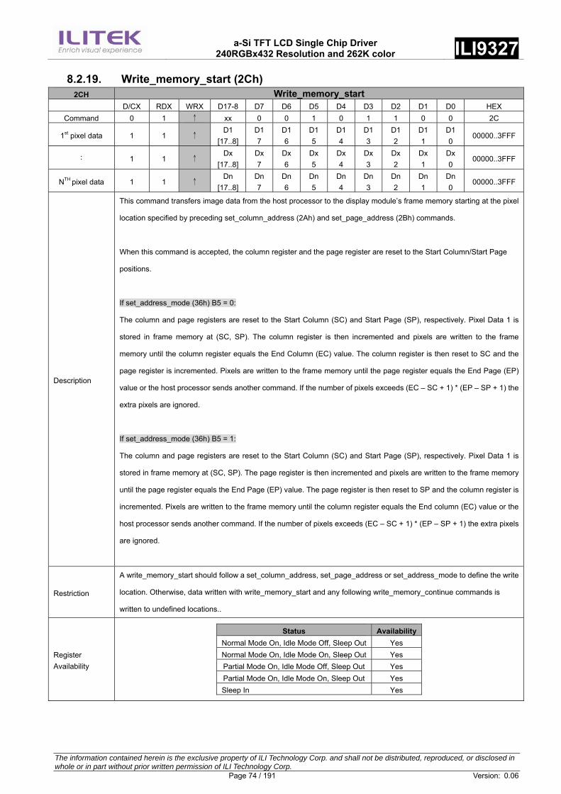
a-Si TFT LCD Single Chip Driver
240RGBx432 Resolution and 262K color ILI9327
The information contained herein is the exclusive property of ILI Technology Corp. and shall not be distributed, reproduced, or disclosed in whole or in part without prior written permission of ILI Technology Corp. Page 74 / 191 Version: 0.06
8.2.19. Write_memory_start (2Ch) 2CH Write_memory_start
D/CX RDX WRX D17-8 D7 D6 D5 D4 D3 D2 D1 D0 HEX Command 0 1 ↑ xx 0 0 1 0 1 1 0 0 2C
1st pixel data 1 1 ↑ D1 [17..8]
D1 7
D1 6
D1 5
D1 4
D1 3
D1 2
D1 1
D1 0
00000..3FFF
︰ 1 1 ↑ Dx [17..8]
Dx 7
Dx 6
Dx 5
Dx 4
Dx 3
Dx 2
Dx 1
Dx 0
00000..3FFF
NTH pixel data 1 1 ↑ Dn [17..8]
Dn 7
Dn 6
Dn 5
Dn 4
Dn 3
Dn 2
Dn 1
Dn 0
00000..3FFF
Description
This command transfers image data from the host processor to the display module’s frame memory starting at the pixel
location specified by preceding set_column_address (2Ah) and set_page_address (2Bh) commands.
When this command is accepted, the column register and the page register are reset to the Start Column/Start Page
positions.
If set_address_mode (36h) B5 = 0:
The column and page registers are reset to the Start Column (SC) and Start Page (SP), respectively. Pixel Data 1 is
stored in frame memory at (SC, SP). The column register is then incremented and pixels are written to the frame
memory until the column register equals the End Column (EC) value. The column register is then reset to SC and the
page register is incremented. Pixels are written to the frame memory until the page register equals the End Page (EP)
value or the host processor sends another command. If the number of pixels exceeds (EC – SC + 1) * (EP – SP + 1) the
extra pixels are ignored.
If set_address_mode (36h) B5 = 1:
The column and page registers are reset to the Start Column (SC) and Start Page (SP), respectively. Pixel Data 1 is
stored in frame memory at (SC, SP). The page register is then incremented and pixels are written to the frame memory
until the page register equals the End Page (EP) value. The page register is then reset to SP and the column register is
incremented. Pixels are written to the frame memory until the column register equals the End column (EC) value or the
host processor sends another command. If the number of pixels exceeds (EC – SC + 1) * (EP – SP + 1) the extra pixels
are ignored.
Restriction
A write_memory_start should follow a set_column_address, set_page_address or set_address_mode to define the write
location. Otherwise, data written with write_memory_start and any following write_memory_continue commands is
written to undefined locations..
Register Availability
Status Availability Normal Mode On, Idle Mode Off, Sleep Out Yes Normal Mode On, Idle Mode On, Sleep Out Yes Partial Mode On, Idle Mode Off, Sleep Out Yes Partial Mode On, Idle Mode On, Sleep Out Yes Sleep In Yes
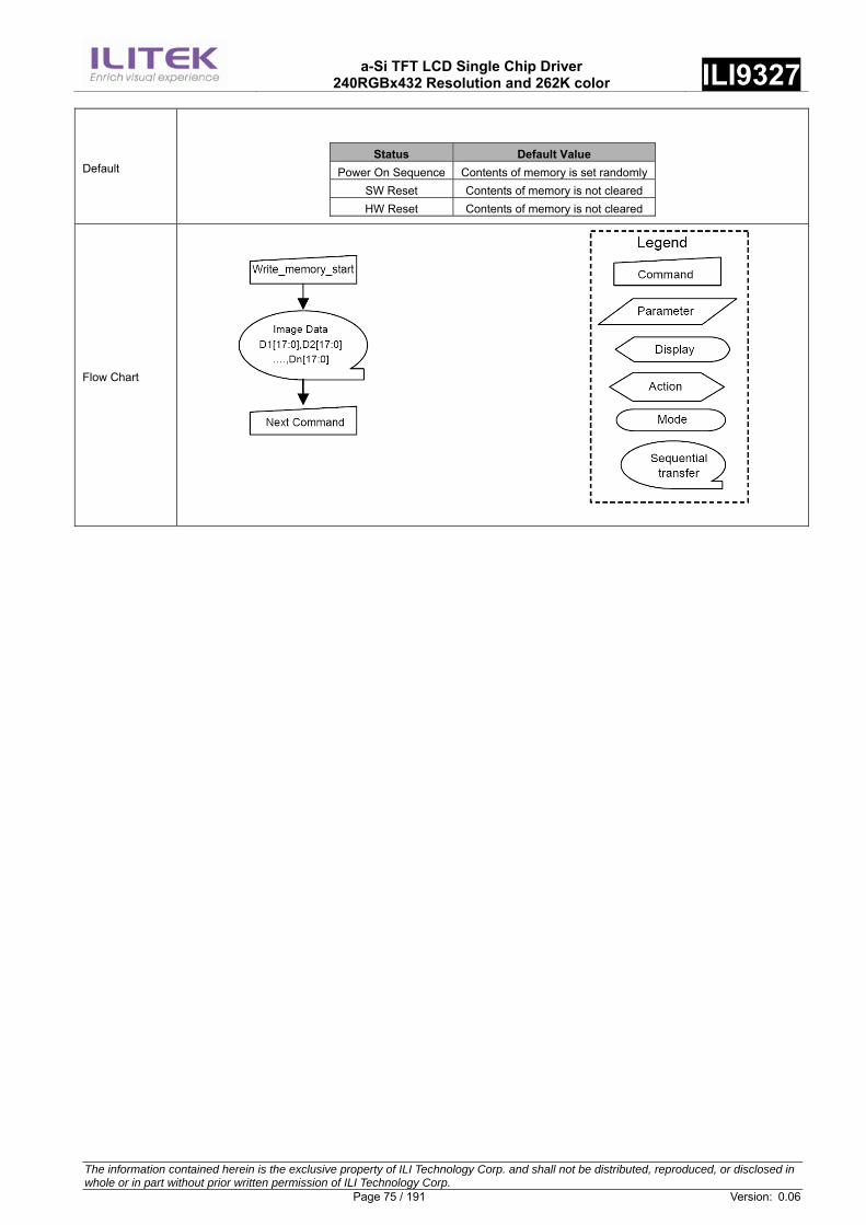
a-Si TFT LCD Single Chip Driver
240RGBx432 Resolution and 262K color ILI9327
The information contained herein is the exclusive property of ILI Technology Corp. and shall not be distributed, reproduced, or disclosed in whole or in part without prior written permission of ILI Technology Corp. Page 75 / 191 Version: 0.06
Default
Status Default Value
Power On Sequence Contents of memory is set randomly SW Reset Contents of memory is not cleared HW Reset Contents of memory is not cleared
Flow Chart

a-Si TFT LCD Single Chip Driver
240RGBx432 Resolution and 262K color ILI9327
The information contained herein is the exclusive property of ILI Technology Corp. and shall not be distributed, reproduced, or disclosed in whole or in part without prior written permission of ILI Technology Corp. Page 76 / 191 Version: 0.06
8.2.20. Read_memory_start (2Eh) 2EH RAMRD (Memory Read)
D/CX RDX WRX D17-8 D7 D6 D5 D4 D3 D2 D1 D0 HEX Command 0 1 ↑ x 0 0 1 0 1 1 1 0 2E
1st Parameter 1 ↑ 1 x x x x x x x x x x
2nd Parameter 1 ↑ 1 D1
[17..8]D1 7
D1 6
D1 5
D1 4
D1 3
D1 2
D1 1
D1 0
00000..3FF
︰ 1 ↑ 1 Dx
[17..8]Dx 7
Dx 6
Dx 5
Dx 4
Dx 3
Dx 2
Dx 1
Dx 0
00000..3FF
(N+1)TH
Parameter 1 ↑ 1
Dn [17..8]
Dn 7
Dn 6
Dn 5
Dn 4
Dn 3
Dn 2
Dn 1
Dn 0
00000..3FF
Description
This command transfers image data from the display module’s frame memory to the host processor starting at the pixel
location specified by preceding set_column_address and set_page_address commands.
If set_address_mode B5 = 0:
The column and page registers are reset to the Start Column (SC) and Start Page (SP), respectively. Pixels are read
from frame memory at (SC, SP). The column register is then incremented and pixels read from the frame memory until
the column register equals the End Column (EC) value. The column register is then reset to SC and the page register is
incremented. Pixels are read from the frame memory until the page register equals the End Page (EP) value or the host
processor sends another command.
If set_address_mode B5 = 1:
The column and page registers are reset to the Start Column (SC) and Start Page (SP), respectively. Pixels are read
from frame memory at (SC, SP). The page register is then incremented and pixels read from the frame memory until the
page register equals the End Page (EP) value. The page register is then reset to SP and the column register is
incremented. Pixels are read from the frame memory until the column register equals the End Column (EC) value or the
host processor sends another command.
Restriction Regardless of the color mode set in set_pixel_format, the pixel format returned by read_memory_continue is always
24-bit so there is no restriction on the length of data.
Register Availability
Status Availability Normal Mode On, Idle Mode Off, Sleep Out Yes Normal Mode On, Idle Mode On, Sleep Out Yes Partial Mode On, Idle Mode Off, Sleep Out Yes Partial Mode On, Idle Mode On, Sleep Out Yes Sleep In Yes
Default
Status Default Value Power On Sequence Contents of memory is set randomly
SW Reset Contents of memory is not cleared HW Reset Contents of memory is not cleared

a-Si TFT LCD Single Chip Driver
240RGBx432 Resolution and 262K color ILI9327
The information contained herein is the exclusive property of ILI Technology Corp. and shall not be distributed, reproduced, or disclosed in whole or in part without prior written permission of ILI Technology Corp. Page 77 / 191 Version: 0.06
Flow Chart

a-Si TFT LCD Single Chip Driver
240RGBx432 Resolution and 262K color ILI9327
The information contained herein is the exclusive property of ILI Technology Corp. and shall not be distributed, reproduced, or disclosed in whole or in part without prior written permission of ILI Technology Corp. Page 78 / 191 Version: 0.06
8.2.21. Set_partial_area (30h) 30H Set_partial_area
D/CX RDX WRX D17-8 D7 D6 D5 D4 D3 D2 D1 D0 HEX Command 0 1 ↑ x 0 0 1 1 0 0 0 0 30
1st Parameter 1 1 ↑ x 0 0 0 0 0 0 0 SR8 000..1DFh
2nd Parameter 1 1 ↑ x SR7 SR6 SR5 SR4 SR3 SR2 SR1 SR0 3rd Parameter 1 1 ↑ x 0 0 0 0 0 0 0 ER8
000..1DFh4th Parameter 1 1 ↑ x ER7 ER6 ER5 ER4 ER3 ER2 ER1 ER0
Description
This command defines the Partial Display mode’s display area. There are two parameters associated with this
command, the first defines the Start Row (SR) and the second the End Row (ER), as illustrated in the following figure.
SR and ER refer to the Frame Memory
If End Row > Start Row and set_address_mode B4 = 0:
SR[8:0]
ER[8:0]
Start Row
End Row
Partial Area
If End Row > Start Row and set_address_mode B4 = 1:
SR[8:0]
ER[8:0]
Start Row
End Row
Partial Area

a-Si TFT LCD Single Chip Driver
240RGBx432 Resolution and 262K color ILI9327
The information contained herein is the exclusive property of ILI Technology Corp. and shall not be distributed, reproduced, or disclosed in whole or in part without prior written permission of ILI Technology Corp. Page 79 / 191 Version: 0.06
End Row < Start Row (set_address_mode(36h) B4=0)
SR[8:0]
ER[8:0]Partial Area
Partial Area
End Row < Start Row (set_address_mode(36h) B4=1)
SR[8:0]
ER[8:0]
End Row
Start Row Partial Area
Partial Area
If End Row = Start Row then the Partial Area will be one row deep.
Restriction SR[15:0] and ER[15:0] cannot be 0000h nor exceed the last vertical line number (01DFh).
Register Availability
Status Availability Normal Mode On, Idle Mode Off, Sleep Out Yes Normal Mode On, Idle Mode On, Sleep Out Yes Partial Mode On, Idle Mode Off, Sleep Out Yes Partial Mode On, Idle Mode On, Sleep Out Yes Sleep In Yes
Default
Status Default Value Power On Sequence SR[8:0]=0000HEX ER[8:0]=1AFHEX
SW Reset SR[8:0]=0000HEX ER[8:0]=1AFHEX HW Reset SR[8:0]=0000HEX ER[8:0]=1AFHEX
Flow Chart 1. To Enter Partial Mode

a-Si TFT LCD Single Chip Driver
240RGBx432 Resolution and 262K color ILI9327
The information contained herein is the exclusive property of ILI Technology Corp. and shall not be distributed, reproduced, or disclosed in whole or in part without prior written permission of ILI Technology Corp. Page 80 / 191 Version: 0.06
2. To Leave Partial Mode
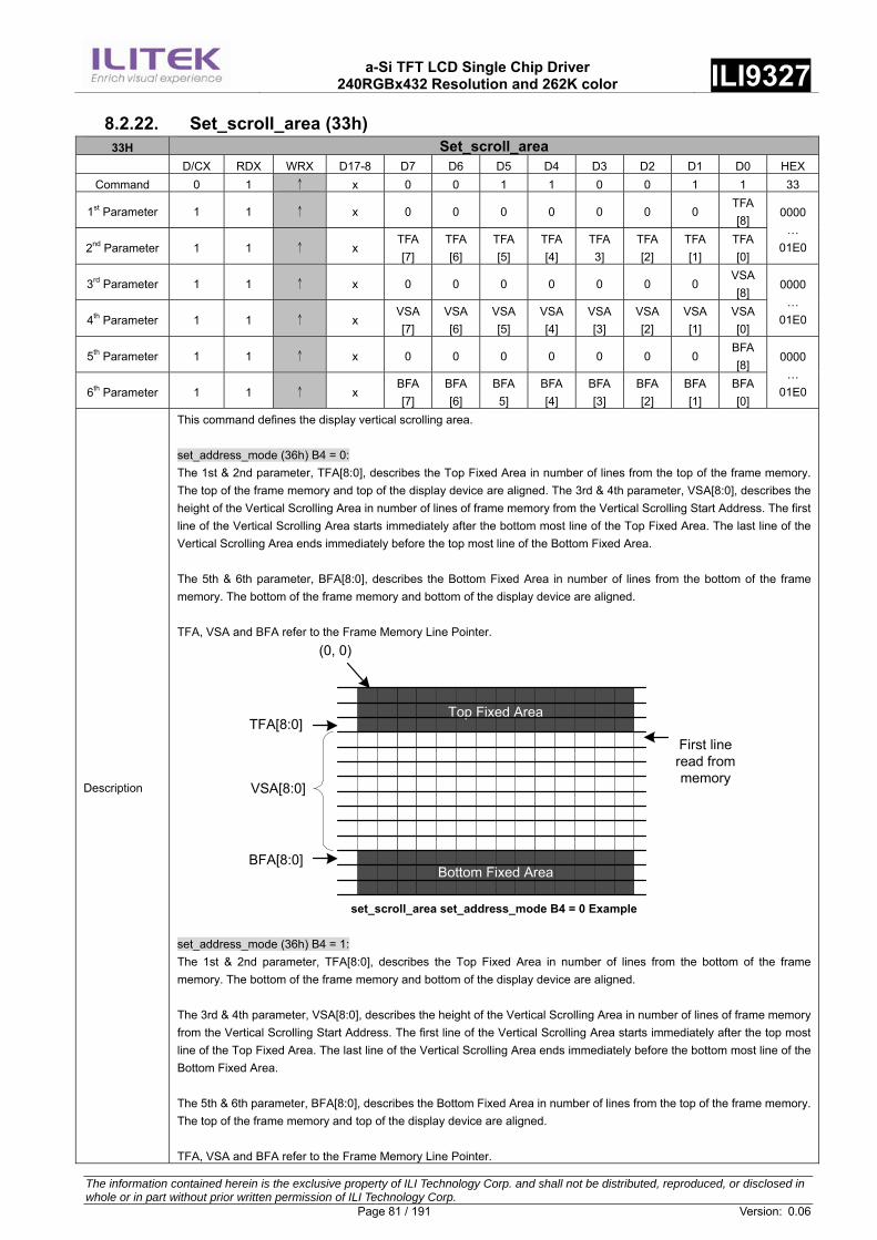
a-Si TFT LCD Single Chip Driver
240RGBx432 Resolution and 262K color ILI9327
The information contained herein is the exclusive property of ILI Technology Corp. and shall not be distributed, reproduced, or disclosed in whole or in part without prior written permission of ILI Technology Corp. Page 81 / 191 Version: 0.06
8.2.22. Set_scroll_area (33h) 33H Set_scroll_area
D/CX RDX WRX D17-8 D7 D6 D5 D4 D3 D2 D1 D0 HEX Command 0 1 ↑ x 0 0 1 1 0 0 1 1 33
1st Parameter 1 1 ↑ x 0 0 0 0 0 0 0 TFA[8]
0000…
01E02nd Parameter 1 1 ↑ x TFA[7]
TFA[6]
TFA[5]
TFA[4]
TFA3]
TFA [2]
TFA [1]
TFA[0]
3rd Parameter 1 1 ↑ x 0 0 0 0 0 0 0 VSA[8]
0000…
01E04th Parameter 1 1 ↑ x VSA[7]
VSA[6]
VSA[5]
VSA[4]
VSA[3]
VSA [2]
VSA [1]
VSA[0]
5th Parameter 1 1 ↑ x 0 0 0 0 0 0 0 BFA[8]
0000…
01E06th Parameter 1 1 ↑ x BFA[7]
BFA[6]
BFA5]
BFA[4]
BFA[3]
BFA [2]
BFA [1]
BFA[0]
Description
This command defines the display vertical scrolling area. set_address_mode (36h) B4 = 0: The 1st & 2nd parameter, TFA[8:0], describes the Top Fixed Area in number of lines from the top of the frame memory. The top of the frame memory and top of the display device are aligned. The 3rd & 4th parameter, VSA[8:0], describes the height of the Vertical Scrolling Area in number of lines of frame memory from the Vertical Scrolling Start Address. The first line of the Vertical Scrolling Area starts immediately after the bottom most line of the Top Fixed Area. The last line of the Vertical Scrolling Area ends immediately before the top most line of the Bottom Fixed Area. The 5th & 6th parameter, BFA[8:0], describes the Bottom Fixed Area in number of lines from the bottom of the frame memory. The bottom of the frame memory and bottom of the display device are aligned. TFA, VSA and BFA refer to the Frame Memory Line Pointer.
Top Fixed Area
Bottom Fixed Area
TFA[8:0]
BFA[8:0]
VSA[8:0]
(0, 0)
First line read from memory
set_scroll_area set_address_mode B4 = 0 Example
set_address_mode (36h) B4 = 1: The 1st & 2nd parameter, TFA[8:0], describes the Top Fixed Area in number of lines from the bottom of the frame memory. The bottom of the frame memory and bottom of the display device are aligned. The 3rd & 4th parameter, VSA[8:0], describes the height of the Vertical Scrolling Area in number of lines of frame memory from the Vertical Scrolling Start Address. The first line of the Vertical Scrolling Area starts immediately after the top most line of the Top Fixed Area. The last line of the Vertical Scrolling Area ends immediately before the bottom most line of the Bottom Fixed Area. The 5th & 6th parameter, BFA[8:0], describes the Bottom Fixed Area in number of lines from the top of the frame memory. The top of the frame memory and top of the display device are aligned. TFA, VSA and BFA refer to the Frame Memory Line Pointer.

a-Si TFT LCD Single Chip Driver
240RGBx432 Resolution and 262K color ILI9327
The information contained herein is the exclusive property of ILI Technology Corp. and shall not be distributed, reproduced, or disclosed in whole or in part without prior written permission of ILI Technology Corp. Page 82 / 191 Version: 0.06
Bottom Fixed Area
Top Fixed AreaTFA[8:0]
BFA[8:0]
VSA[8:0]
(0, 0)
First line read from memory
Top Fixed AreaTop Fixed Area
set_scroll_area set_address_mode B4 = 1 Example
Restriction
The sum of TFA, VSA and BFA must equal the number of the display device’s horizontal lines (pages), otherwise Scrolling
mode is undefined. In Vertical Scroll Mode, set_address_mode B5 should be set to ‘0’ – this only affects the Frame
Memory Write.
Register Availability
Status Availability Normal Mode On, Idle Mode Off, Sleep Out Yes Normal Mode On, Idle Mode On, Sleep Out Yes Partial Mode On, Idle Mode Off, Sleep Out Yes Partial Mode On, Idle Mode On, Sleep Out Yes Sleep In Yes
Default
Status Default Value Power On Sequence TFA[8:0]=0000HEX VSA[8:0]=01B0HEX BFA[8:0]=0000HEX
SW Reset TFA [8:0]=0000HEX VSA[8:0]=01B0HEX BFA[8:0]=0000HEX HW Reset TFA [8:0]=0000HEX VSA[8:0]=01B0HEX BFA[8:0]=0000HEX
Flow Chart
1. To enter Vertical Scroll Mode:
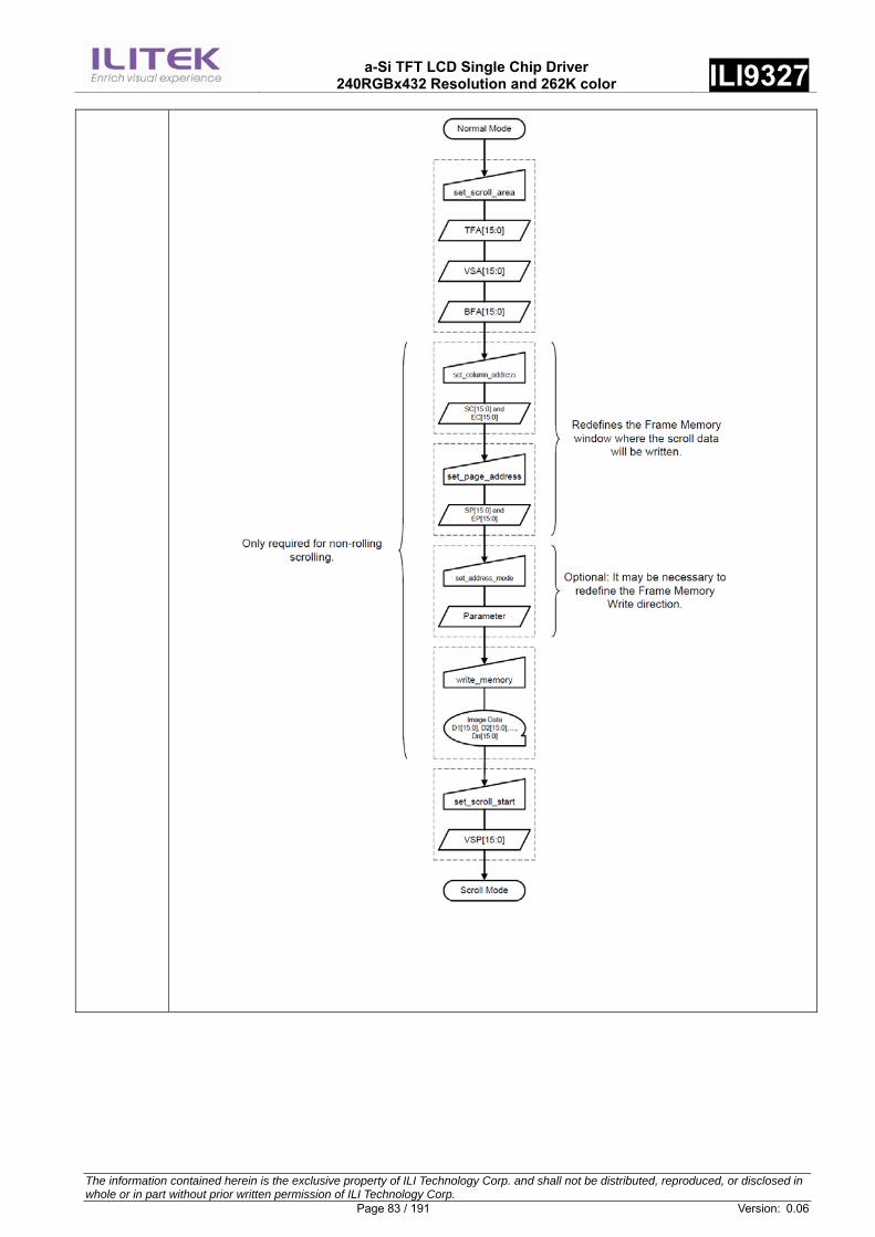
a-Si TFT LCD Single Chip Driver
240RGBx432 Resolution and 262K color ILI9327
The information contained herein is the exclusive property of ILI Technology Corp. and shall not be distributed, reproduced, or disclosed in whole or in part without prior written permission of ILI Technology Corp. Page 83 / 191 Version: 0.06

a-Si TFT LCD Single Chip Driver
240RGBx432 Resolution and 262K color ILI9327
The information contained herein is the exclusive property of ILI Technology Corp. and shall not be distributed, reproduced, or disclosed in whole or in part without prior written permission of ILI Technology Corp. Page 84 / 191 Version: 0.06
8.2.23. Set_tear_off (34h) 34H Set_tear_off
D/CX RDX WRX D17-8 D7 D6 D5 D4 D3 D2 D1 D0 HEX Command 0 1 ↑ x 0 0 1 1 0 1 0 0 34 Parameter NO PARAMETER
Description This command turns off the display module’s Tearing Effect output signal on the TE signal line.
Restriction This command has no effect when the Tearing Effect output is already off.
Register Availability
Status Availability Normal Mode On, Idle Mode Off, Sleep Out Yes Normal Mode On, Idle Mode On, Sleep Out Yes Partial Mode On, Idle Mode Off, Sleep Out Yes Partial Mode On, Idle Mode On, Sleep Out Yes Sleep In Yes
Default
Status Default ValuePower On Sequence OFF SW Reset OFF HW Reset OFF
Flow Chart
8.2.24. Set_tear_on (35h) 35H Set_tear_on
D/CX RDX WRX D17-8 D7 D6 D5 D4 D3 D2 D1 D0 HEX Command 0 1 ↑ x 0 0 1 1 0 1 0 1 35
1st Parameter 1 1 ↑ x x x x x x x x TELOM xx
Description
This command turns on the tearing Effect output signal on the TE signal line. The TE signal is not affected by changing
set_address_mode (36h) bit B4 (Line Address Order).
The Tearing Effect Line On has one parameter that describes the Tearing Effect Output Line mode.
If TELOM = 0:
The Tearing Effect Output line consists of V-Blanking information only.

a-Si TFT LCD Single Chip Driver
240RGBx432 Resolution and 262K color ILI9327
The information contained herein is the exclusive property of ILI Technology Corp. and shall not be distributed, reproduced, or disclosed in whole or in part without prior written permission of ILI Technology Corp. Page 85 / 191 Version: 0.06
tvdl tvdh
Vertical Time Scale
If TELOM = 1:
The Tearing Effect Output Line consists of both V-Blanking and H-Blanking information.
tvdl
V-Sync
tvdh
1st Line 480th
Line
V-SyncInvisible
Line
The Tearing Effect Output line shall be active low when the display module is in Sleep mode.
Restriction This command has no effect when Tearing Effect output is already ON.
Register Availability
Status Availability Normal Mode On, Idle Mode Off, Sleep Out Yes Normal Mode On, Idle Mode On, Sleep Out Yes Partial Mode On, Idle Mode Off, Sleep Out Yes Partial Mode On, Idle Mode On, Sleep Out Yes Sleep In Yes
Default
Status Default ValuePower On Sequence OFF
SW Reset OFF HW Reset OFF
Flow Chart

a-Si TFT LCD Single Chip Driver
240RGBx432 Resolution and 262K color ILI9327
The information contained herein is the exclusive property of ILI Technology Corp. and shall not be distributed, reproduced, or disclosed in whole or in part without prior written permission of ILI Technology Corp. Page 86 / 191 Version: 0.06
8.2.25. Set_address_mode (36h) 36H Set_address_mode
D/CX RDX WRX D17-8 D7 D6 D5 D4 D3 D2 D1 D0 HEX Command 0 1 ↑ x 0 0 1 1 0 1 1 0 36
1st Parameter 1 1 ↑ x B7 B6 B5 B4 B3 0 B1 B0 xx
Description
This command defines read/write scanning direction of frame memory.
This command makes no change on the other driver status.
Bit Description Comment B7 Page Address Order B6 Column Address Order B5 Page/Column Selection B4 Vertical Order B3 RGB/BGR Order B2 Display data latch data order Set to ‘0’ B1 Horizontal Flip B0 Vertical Flip
・Bit B7 – Page Address Order
‘0’ = Top to Bottom
‘1’ = Bottom to Top
・Bit B6 – Column Address Order
‘0’ = Left to Right
‘1’ = Right to Left
・Bit B5 – Page/Column Order
‘0’ = Normal Mode
‘1’ = Reverse Mode
・Bit B4 –Line Address Order
‘0’ = LCD Refresh Top to Bottom
‘1’ = LCD Refresh Bottom to Top
・Bit B3 – RGB/BGR Order
‘0’ = Pixels sent in RGB order
‘1’ = Pixels sent in BGR order
・Bit B2 –Display Data Latch Data Order
This bit is not applicable for this project, so it is set to ‘0’. (Not supported)
・Bit B1 – Horizontal Flip
‘0’ = Normal display
‘1’ = Flipped display
・Bit B0 – Vertical Flip
‘0’ = Normal display
‘1’ = Flipped display
X = Don’t care

a-Si TFT LCD Single Chip Driver
240RGBx432 Resolution and 262K color ILI9327
The information contained herein is the exclusive property of ILI Technology Corp. and shall not be distributed, reproduced, or disclosed in whole or in part without prior written permission of ILI Technology Corp. Page 87 / 191 Version: 0.06
B5 B6 B7 Image in Frame Memory
B
E
000
B
E
B
E
B
E
100
010
110
B5 B6 B7 Image in Frame Memory
001
101
011
111
B
E
B
E
B
E
B
E
R G B R G B
B3 = 0
Sent RGBMemory Display Panel
R G B RGBSent BGR
Memory Display Panel
B3 = 1
Restriction
Register Availability
Status Availability Normal Mode On, Idle Mode Off, Sleep Out Yes Normal Mode On, Idle Mode On, Sleep Out Yes Partial Mode On, Idle Mode Off, Sleep Out Yes Partial Mode On, Idle Mode On, Sleep Out Yes Sleep In Yes

a-Si TFT LCD Single Chip Driver
240RGBx432 Resolution and 262K color ILI9327
The information contained herein is the exclusive property of ILI Technology Corp. and shall not be distributed, reproduced, or disclosed in whole or in part without prior written permission of ILI Technology Corp. Page 88 / 191 Version: 0.06
Default
Status Default Value Power On Sequence 00HEX
SW Reset No Change HW Reset 00HEX
Flow Chart

a-Si TFT LCD Single Chip Driver
240RGBx432 Resolution and 262K color ILI9327
The information contained herein is the exclusive property of ILI Technology Corp. and shall not be distributed, reproduced, or disclosed in whole or in part without prior written permission of ILI Technology Corp. Page 89 / 191 Version: 0.06
8.2.26. Set_scroll_start (37h) 37H Set_scroll_start
D/CX RDX WRX D17-8 D7 D6 D5 D4 D3 D2 D1 D0 HEXCommand 0 1 ↑ x 0 0 1 1 0 1 1 1 37
1st Parameter
1 1 ↑ x 0 0 0 0 0 0 0 VSP[8]
xx
2nd Parameter
1 1 ↑ x VSP[7]
VSP[6]
VSP[5]
VSP[4]
VSP[3]
VSP [2]
VSP [1]
VSP[0]
xx
Description
This command sets the start of the vertical scrolling area in the frame memory. The vertical scrolling area is fully defined when this command is used with the set_scroll_area command The set_scroll_start command has one parameter, the Vertical Scroll Pointer. The VSP defines the line in the frame memory that is written to the display device as the first line of the vertical scroll area. The displayed image also depends on the setting of the Line Address Order bit, B4, in the set_address_mode register. See the examples below.
If set_address_mode (R36h) B4 = 0:
Example:
When Top Fixed Area = Bottom Fixed Area = 0, Vertical Scrolling Area = 432 and VSP = 3.
Frame Memory
(0, 0)
VSP[8:0]
(0, 431)
0
PointerB4=0
1
2
3
4
..
..
429
430
431
Display
If set_address_mode (R36h) B4 = 1:
Example: When Top Fixed Area = Bottom Fixed Area = 00, Vertical Scrolling Area = 432 and VSP=’3’.
Frame Memory
(0, 0)
VSP[8:0]
(0, 431)
0
PointerB4=1
1
2
3
4
..
..
429
430
431
Display
Note: When new Pointer position and Picture Data are sent, the result on the display will happen at the next Panel Scan to avoid
tearing effect. VSP refers to the Frame Memory line Pointer.
Restriction
Since the value of the Vertical Scrolling Start Address is absolute (with reference to the Frame Memory), it must not enter the fixed area (defined by Vertical Scrolling Definition (33h) – otherwise undesirable image will be displayed on the Panel.

a-Si TFT LCD Single Chip Driver
240RGBx432 Resolution and 262K color ILI9327
The information contained herein is the exclusive property of ILI Technology Corp. and shall not be distributed, reproduced, or disclosed in whole or in part without prior written permission of ILI Technology Corp. Page 90 / 191 Version: 0.06
Register Availability
Status Availability Normal Mode On, Idle Mode Off, Sleep Out Yes Normal Mode On, Idle Mode On, Sleep Out Yes Partial Mode On, Idle Mode Off, Sleep Out No Partial Mode On, Idle Mode On, Sleep Out No Sleep In Yes
Default
Status Default ValuePower On Sequence 0000HEX
SW Reset 0000HEX HW Reset 0000HEX
Flow Chart
Refer to the description set_scroll_area (33h)

a-Si TFT LCD Single Chip Driver
240RGBx432 Resolution and 262K color ILI9327
The information contained herein is the exclusive property of ILI Technology Corp. and shall not be distributed, reproduced, or disclosed in whole or in part without prior written permission of ILI Technology Corp. Page 91 / 191 Version: 0.06
8.2.27. Exit_idle_mode (38h) 38H Exit_idle_mode
D/CX RDX WRX D17-8 D7 D6 D5 D4 D3 D2 D1 D0 HEX Command 0 1 ↑ x 0 0 1 1 1 0 0 0 38 Parameter NO PARAMETER
Description This command causes the display module to exit Idle mode.
Restriction This command has no effect when the display module is not in Idle mode.
Register Availability
Status Availability Normal Mode On, Idle Mode Off, Sleep Out Yes Normal Mode On, Idle Mode On, Sleep Out Yes Partial Mode On, Idle Mode Off, Sleep Out Yes Partial Mode On, Idle Mode On, Sleep Out Yes Sleep In Yes
Default
Status Default Value Power On Sequence Idle Mode Off
SW Reset Idle Mode Off HW Reset Idle Mode Off
Flow Chart
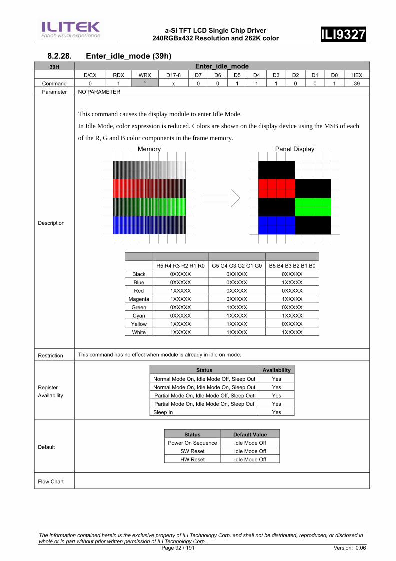
a-Si TFT LCD Single Chip Driver
240RGBx432 Resolution and 262K color ILI9327
The information contained herein is the exclusive property of ILI Technology Corp. and shall not be distributed, reproduced, or disclosed in whole or in part without prior written permission of ILI Technology Corp. Page 92 / 191 Version: 0.06
8.2.28. Enter_idle_mode (39h) 39H Enter_idle_mode
D/CX RDX WRX D17-8 D7 D6 D5 D4 D3 D2 D1 D0 HEX Command 0 1 ↑ x 0 0 1 1 1 0 0 1 39 Parameter NO PARAMETER
Description
This command causes the display module to enter Idle Mode.
In Idle Mode, color expression is reduced. Colors are shown on the display device using the MSB of each
of the R, G and B color components in the frame memory.
Memory Panel Display
R5 R4 R3 R2 R1 R0 G5 G4 G3 G2 G1 G0 B5 B4 B3 B2 B1 B0
Black 0XXXXX 0XXXXX 0XXXXX Blue 0XXXXX 0XXXXX 1XXXXX Red 1XXXXX 0XXXXX 0XXXXX
Magenta 1XXXXX 0XXXXX 1XXXXX Green 0XXXXX 1XXXXX 0XXXXX Cyan 0XXXXX 1XXXXX 1XXXXX
Yellow 1XXXXX 1XXXXX 0XXXXX White 1XXXXX 1XXXXX 1XXXXX
Restriction This command has no effect when module is already in idle on mode.
Register Availability
Status Availability Normal Mode On, Idle Mode Off, Sleep Out Yes Normal Mode On, Idle Mode On, Sleep Out Yes Partial Mode On, Idle Mode Off, Sleep Out Yes Partial Mode On, Idle Mode On, Sleep Out Yes Sleep In Yes
Default
Status Default Value Power On Sequence Idle Mode Off
SW Reset Idle Mode Off HW Reset Idle Mode Off
Flow Chart
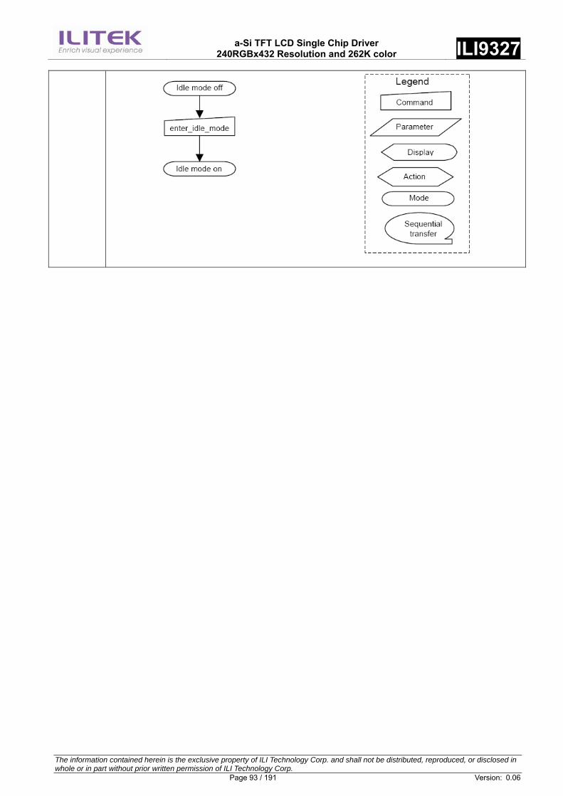
a-Si TFT LCD Single Chip Driver
240RGBx432 Resolution and 262K color ILI9327
The information contained herein is the exclusive property of ILI Technology Corp. and shall not be distributed, reproduced, or disclosed in whole or in part without prior written permission of ILI Technology Corp. Page 93 / 191 Version: 0.06

a-Si TFT LCD Single Chip Driver
240RGBx432 Resolution and 262K color ILI9327
The information contained herein is the exclusive property of ILI Technology Corp. and shall not be distributed, reproduced, or disclosed in whole or in part without prior written permission of ILI Technology Corp. Page 94 / 191 Version: 0.06
8.2.29. Set_pixel_format (3Ah) 3AH Set_pixel_format
D/CX RDX WRX D17-8 D7 D6 D5 D4 D3 D2 D1 D0 HEX Command 0 1 ↑ x 0 0 1 1 1 0 1 0 3A
1st Parameter 1 1 ↑ x x D6 D5 D4 x D2 D1 D0 66
Description
This command sets the pixel format for the RGB image data used by the interface.
Bits D[6:4] – DPI Pixel Format Definition
Bits D[2:0] – DBI Pixel Format Definition
Bits D7 and D3 are not used.
If a particular interface, either DBI or DPI, is not used then the corresponding bits in the parameter
are ignored.
Control Interface Color Format D6/D2 D5/D1 D4/D0 Not defined 0 0 0
3bit/pixel (8 color) 0 0 1 Not defined 0 1 0 Not defined 0 1 1 Not defined 1 0 0
16bit/pixel (65,536 colors) 1 0 1 18bit/pixel (262,144 colors) 1 1 0
Not defined 1 1 1
Restriction There is no visible effect until the Frame Memory is written to.
Register Availability
Status Availability Normal Mode On, Idle Mode Off, Sleep Out Yes Normal Mode On, Idle Mode On, Sleep Out Yes Partial Mode On, Idle Mode Off, Sleep Out Yes Partial Mode On, Idle Mode On, Sleep Out Yes Sleep In Yes
Default
Status Default Value Power On Sequence 66HEX SW Reset 66HEX HW Reset 66HEX

a-Si TFT LCD Single Chip Driver
240RGBx432 Resolution and 262K color ILI9327
The information contained herein is the exclusive property of ILI Technology Corp. and shall not be distributed, reproduced, or disclosed in whole or in part without prior written permission of ILI Technology Corp. Page 95 / 191 Version: 0.06
Flow Chart

a-Si TFT LCD Single Chip Driver
240RGBx432 Resolution and 262K color ILI9327
The information contained herein is the exclusive property of ILI Technology Corp. and shall not be distributed, reproduced, or disclosed in whole or in part without prior written permission of ILI Technology Corp. Page 96 / 191 Version: 0.06
8.2.30. Write_Memory_Continue (3Ch) 3CH Write_Memory_Continue
D/CX RDX WRX D17-8 D7 D6 D5 D4 D3 D2 D1 D0 HEX Command 0 1 ↑ x 0 0 1 1 1 1 0 0 3C
1st Parameter 1 1 ↑ D1 [17..8]
D1 [7]
D1 [6]
D1 [5]
D1 [4]
D1 [3]
D1 [2]
D1 [1]
D1 [0]
000 3FF
xst Parameter 1 1 ↑ Dx [17..8]
Dx [7]
Dx [6]
Dx [5]
Dx [4]
Dx [3]
Dx [2]
Dx [1]
Dx [0]
000 3FF
Nst Parameter 1 1 ↑ Dn [17..8]
Dn [7]
Dn [6]
Dn [5]
Dn [4]
Dn [3]
Dn [2]
Dn [1]
Dn [0]
000 3FF
Description
This command transfers image data from the host processor to the display module’s frame memory continuing from the
pixel location following the previous write_memory_continue or write_memory_start command.
If set_address_mode B5 = 0:
Data is written continuing from the pixel location after the write range of the previous write_memory_start or
write_memory_continue. The column register is then incremented and pixels are written to the frame memory until the
column register equals the End Column (EC) value. The column register is then reset to SC and the page register is
incremented. Pixels are written to the frame memory until the page register equals the End Page (EP) value and the
column register equals the EC value, or the host processor sends another command. If the number of pixels exceeds (EC –
SC + 1) * (EP – SP + 1) the extra pixels are ignored.
If set_address_mode B5 = 1:
Data is written continuing from the pixel location after the write range of the previous write_memory_start or
write_memory_continue. The page register is then incremented and pixels are written to the frame memory until the page
register equals the End Page (EP) value. The page register is then reset to SP and the column register is incremented.
Pixels are written to the frame memory until the column register equals the End column (EC) value and the page register
equals the EP value, or the host processor sends another command. If the number of pixels exceeds (EC – SC + 1) * (EP –
SP + 1) the extra pixels are ignored.
Sending any other command can stop frame Write.
Frame Memory Access and Interface setting (B3h), WEMODE=0
When the transfer number of data exceeds (EC-SC+1)*(EP-SP+1), the exceeding data will be ignored.
Frame Memory Access and Interface setting (B3h), WEMODE=1
When the transfer number of data exceeds (EC-SC+1)*(EP-SP+1), the column and page number will be reset, and the
exceeding data will be written into the following column and page.
Restriction A write_memory_start should follow a set_column_address, set_page_address or set_address_mode to define the write
address. Otherwise, data written with write_memory_continue is written to undefined addresses.

a-Si TFT LCD Single Chip Driver
240RGBx432 Resolution and 262K color ILI9327
The information contained herein is the exclusive property of ILI Technology Corp. and shall not be distributed, reproduced, or disclosed in whole or in part without prior written permission of ILI Technology Corp. Page 97 / 191 Version: 0.06
Register Availability
Status Availability Normal Mode On, Idle Mode Off, Sleep Out Yes Normal Mode On, Idle Mode On, Sleep Out Yes Partial Mode On, Idle Mode Off, Sleep Out Yes Partial Mode On, Idle Mode On, Sleep Out Yes Sleep In No
Default
Status Default Value Power On Sequence Random value SW Reset No change HW Reset No change
Flow Chart
a-Si TFT LCD Single Chip Driver
240RGBx432 Resolution and 262K color ILI9327
The information contained herein is the exclusive property of ILI Technology Corp. and shall not be distributed, reproduced, or disclosed in whole or in part without prior written permission of ILI Technology Corp. Page 98 / 191 Version: 0.06
8.2.31. Read_Memory_Continue (3Eh) 3EH Read_Memory_Continue
D/CX RDX WRX D17-8 D7 D6 D5 D4 D3 D2 D1 D0 HEX Command 0 1 ↑ x 0 0 1 1 1 1 1 0 3E
1st Parameter 1 ↑ 1 x x x x x x x x x x
2nd Parameter 1 ↑ 1 D1
[17..8] D1 [7]
D1 [6]
D1 [5]
D1 [4]
D1 [3]
D1 [2]
D1 [1]
D1 [0]
000 3FF
xst Parameter 1 ↑ 1 Dx
[17..8] Dx [7]
Dx [6]
Dx [5]
Dx [4]
Dx [3]
Dx [2]
Dx [1]
Dx [0]
000 3FF
Nst Parameter 1 ↑ 1 Dn
[17..8] Dn [7]
Dn [6]
Dn [5]
Dn [4]
Dn [3]
Dn [2]
Dn [1]
Dn [0]
000 3FF
Description
This command transfers image data from the display module’s frame memory to the host processor continuing from the
location following the previous read_memory_continue (3Eh) or read_memory_start (2Eh) command.
If set_address_mode B5 = 0:
Pixels are read continuing from the pixel location after the read range of the previous read_memory_start or
read_memory_continue. The column register is then incremented and pixels are read from the frame memory until the
column register equals the End Column (EC) value. The column register is then reset to SC and the page register is
incremented. Pixels are read from the frame memory until the page register equals the End Page (EP) value and the
column register equals the EC value, or the host processor sends another command.
If set_address_mode B5 = 1:
Pixels are read continuing from the pixel location after the read range of the previous read_memory_start or
read_memory_continue. The page register is then incremented and pixels are read from the frame memory until the page
register equals the End Page (EP) value. The page register is then reset to SP and the column register is incremented.
Pixels are read from the frame memory until the column register equals the End Column (EC) value and the page register
equals the EP value, or the host processor sends another command.
This command makes no change to the other driver status.
Restriction A read_memory_start should follow a set_column_address, set_page_address or set_address_mode to define the read
location. Otherwise, data read with read_memory_continue is undefined.
Register Availability
Status Availability Normal Mode On, Idle Mode Off, Sleep Out Yes Normal Mode On, Idle Mode On, Sleep Out Yes Partial Mode On, Idle Mode Off, Sleep Out Yes Partial Mode On, Idle Mode On, Sleep Out Yes Sleep In Yes
Default
Status Default Value Power On Sequence Random data SW Reset No change HW Reset No change

a-Si TFT LCD Single Chip Driver
240RGBx432 Resolution and 262K color ILI9327
The information contained herein is the exclusive property of ILI Technology Corp. and shall not be distributed, reproduced, or disclosed in whole or in part without prior written permission of ILI Technology Corp. Page 99 / 191 Version: 0.06
Flow Chart
8.2.32. Set_Tear_Scanline (44h) 44H Set_Tear_Scanline
D/CX RDX WRX D17-8 D7 D6 D5 D4 D3 D2 D1 D0 HEX Command 0 1 ↑ x 0 1 0 0 0 1 0 0 44
1st Parameter 1 1 ↑ xx 0 0 0 0 0 0 0 STS[8]
0x
2nd Parameter 1 1 ↑ xx STS[7]
STS[6]
STS[5]
STS[4]
STS [3]
STS [2]
STS [1]
STS[0]
xx
Description
This command turns on the display Tearing Effect output signal on the TE signal line when the display reaches line N. The
TE signal is not affected by changing set_address_mode bit B4. The Tearing Effect Line On has one parameter that
describes the Tearing Effect Output Line mode.
tvdl tvdh
Vertical Time Scale
The Tearing Effect Output line shall be active low when the display module is in Sleep mode.
Restriction -
Register Availability
Status Availability Normal Mode On, Idle Mode Off, Sleep Out Yes Normal Mode On, Idle Mode On, Sleep Out Yes Partial Mode On, Idle Mode Off, Sleep Out Yes Partial Mode On, Idle Mode On, Sleep Out Yes Sleep In Yes

a-Si TFT LCD Single Chip Driver
240RGBx432 Resolution and 262K color ILI9327
The information contained herein is the exclusive property of ILI Technology Corp. and shall not be distributed, reproduced, or disclosed in whole or in part without prior written permission of ILI Technology Corp. Page 100 / 191 Version: 0.06
Default
Status Default Value Power On Sequence 00HEX SW Reset 00HEX HW Reset 00HEX
Flow Chart

a-Si TFT LCD Single Chip Driver
240RGBx432 Resolution and 262K color ILI9327
The information contained herein is the exclusive property of ILI Technology Corp. and shall not be distributed, reproduced, or disclosed in whole or in part without prior written permission of ILI Technology Corp. Page 101 / 191 Version: 0.06
8.2.33. Get_Scanline (45h) 45H Get_Scanline
D/CX RDX WRX D17-8 D7 D6 D5 D4 D3 D2 D1 D0 HEX Command 0 1 ↑ x 0 1 0 0 0 1 0 1 45
1st Parameter 1 ↑ 1 x x x x x x x x x x
2nd Parameter 1 ↑ 1 xx 0 0 0 0 0 0 0 GTS[8]
0x
3rd Parameter 1 ↑ 1 xx GTS[7]
GTS[6]
GTS[5]
GTS[4]
GTS [3]
GTS [2]
GTS [1]
GTS[0]
xx
Description
The display returns the current scan line, N, used to update the display device. The total number of scan lines on a display
device is defined as VSYNC + VBP + VACT + VFP. The first scan line is defined as the first line of V-Sync and is denoted
as Line 0.
When in Sleep Mode, the value returned by get_scanline is undefined.
Restriction None
Register Availability
Status Availability Normal Mode On, Idle Mode Off, Sleep Out Yes Normal Mode On, Idle Mode On, Sleep Out Yes Partial Mode On, Idle Mode Off, Sleep Out Yes Partial Mode On, Idle Mode On, Sleep Out Yes Sleep In Yes
Default
Status Default Value Power On Sequence 00HEX SW Reset 00HEX HW Reset 00HEX
Flow Chart

a-Si TFT LCD Single Chip Driver
240RGBx432 Resolution and 262K color ILI9327
The information contained herein is the exclusive property of ILI Technology Corp. and shall not be distributed, reproduced, or disclosed in whole or in part without prior written permission of ILI Technology Corp. Page 102 / 191 Version: 0.06
8.2.34. Write Display Brightness (51h) 51H WRDISBV (Write Display Brightness)
D/CX RDX WRX D17-8 D7 D6 D5 D4 D3 D2 D1 D0 HEX Command 0 1 ↑ x 0 1 0 1 0 0 0 1 51
1st Parameter 1 ↑ 1 xx DBV[7]
DBV[6]
DBV[5]
DBV[4]
DBV [3]
DBV [2]
DBV [1]
DBV[0]
00 ..
FF
Description
This command is used to adjust the brightness value of the display.
It should be checked what is the relationship between this written value and output brightness of the display. This
relationship is defined on the display module specification.
In principle relationship is that 00h value means the lowest brightness and FFh value means the highest brightness.
Restriction None
Register Availability
Status Availability Normal Mode On, Idle Mode Off, Sleep Out Yes Normal Mode On, Idle Mode On, Sleep Out Yes Partial Mode On, Idle Mode Off, Sleep Out Yes Partial Mode On, Idle Mode On, Sleep Out Yes Sleep In Yes
Default
Status Default Value Power On Sequence 00HEX
SW Reset 00HEX HW Reset 00HEX
Flow Chart

a-Si TFT LCD Single Chip Driver
240RGBx432 Resolution and 262K color ILI9327
The information contained herein is the exclusive property of ILI Technology Corp. and shall not be distributed, reproduced, or disclosed in whole or in part without prior written permission of ILI Technology Corp. Page 103 / 191 Version: 0.06
8.2.35. Read Display Brightness (52h) 52H RDDISBV (Read Display Brightness Value)
D/CX RDX WRX D17-8 D7 D6 D5 D4 D3 D2 D1 D0 HEX Command 0 1 ↑ x 0 1 0 1 0 0 1 0 52
1st Parameter 1 ↑ 1 xx x x x x x x x x x
2nd Parameter 1 ↑ 1 xx DBV[7]
DBV[6]
DBV[5]
DBV[4]
DBV [3]
DBV [2]
DBV [1]
DBV[0]
xx
Description
This command returns the brightness value of the display.
It should be checked what the relationship between this returned value and output brightness of the display. This
relationship is defined on the display module specification.
In principle the relationship is that 00h value means the lowest brightness and FFh value means the highest brightness.
This command can be used to read the brightness value of the display also when Display brightness control is in automatic
mode.
Write CTRL Display (53h)” bit DB = ‘1’.
DBV[7:0] is reset when display is in sleep-in mode.
DBV[7:0] is ‘0’ when bit BCTRL of “Write CTRL Display (53h)” command is ‘0’.
DBV[7:0] is manual set brightness specified with “Write CTRL Display (53h)” command when bit BCTRL is ‘1’ and bit A of
“Write CTRL Display (53h)” command is ‘0’.
Restriction
The display module is sending 2nd parameter value on the data lines if the MCU wants to read more than one parameter (=
more than 2 RDX cycle) on DBI Mode.
Only 2nd parameter is sent on DSI (The 1st parameter is not sent).
Register Availability
Status Availability Normal Mode On, Idle Mode Off, Sleep Out Yes Normal Mode On, Idle Mode On, Sleep Out Yes Partial Mode On, Idle Mode Off, Sleep Out Yes Partial Mode On, Idle Mode On, Sleep Out Yes Sleep In Yes
Default
Status Default Value Power On Sequence 00HEX
SW Reset 00HEX HW Reset 00HEX

a-Si TFT LCD Single Chip Driver
240RGBx432 Resolution and 262K color ILI9327
The information contained herein is the exclusive property of ILI Technology Corp. and shall not be distributed, reproduced, or disclosed in whole or in part without prior written permission of ILI Technology Corp. Page 104 / 191 Version: 0.06
Flow Chart

a-Si TFT LCD Single Chip Driver
240RGBx432 Resolution and 262K color ILI9327
The information contained herein is the exclusive property of ILI Technology Corp. and shall not be distributed, reproduced, or disclosed in whole or in part without prior written permission of ILI Technology Corp. Page 105 / 191 Version: 0.06
8.2.36. Write CTRL Display (53h) 53H WRCTRLD (Write Control Display)
D/CX RDX WRX D17-8 D7 D6 D5 D4 D3 D2 D1 D0 HEX Command 0 1 ↑ x 0 1 0 1 0 0 1 1 53
1st Parameter 1 ↑ 1 xx 0 0 BCTRL 0 DD BL 0 0 xx
Description
This command is used to control display brightness.
BCTRL: Brightness Control Block On/Off, This bit is always used to switch brightness for display.
0 = Off (Brightness registers are 00h, DBV[7..0])
1 = On (Brightness registers are active, according to the other parameters.)
Display Dimming (DD): (Only for manual brightness setting)
DD = 0: Display Dimming is off
DD = 1: Display Dimming is on
BL: Backlight Control On/Off
0 = Off (Completely turn off backlight circuit. Control lines must be low. )
1 = On
Dimming function is adapted to the brightness registers for display when bit BCTRL is changed at DD=1, e.g. BCTRL: 0
1 or 1 0.
When BL bit change from “On” to “Off”, backlight is turned off without gradual dimming, even if dimming-on (DD=1) are
selected.
Restriction None
Register Availability
Status Availability Normal Mode On, Idle Mode Off, Sleep Out Yes Normal Mode On, Idle Mode On, Sleep Out Yes Partial Mode On, Idle Mode Off, Sleep Out Yes Partial Mode On, Idle Mode On, Sleep Out Yes Sleep In Yes
Default
Status Default Value Power On Sequence BCTRL=0, DD=0, BL=0
SW Reset BCTRL=0, DD=0, BL=0 HW Reset BCTRL=0, DD=0, BL=0

a-Si TFT LCD Single Chip Driver
240RGBx432 Resolution and 262K color ILI9327
The information contained herein is the exclusive property of ILI Technology Corp. and shall not be distributed, reproduced, or disclosed in whole or in part without prior written permission of ILI Technology Corp. Page 106 / 191 Version: 0.06
Flow Chart

a-Si TFT LCD Single Chip Driver
240RGBx432 Resolution and 262K color ILI9327
The information contained herein is the exclusive property of ILI Technology Corp. and shall not be distributed, reproduced, or disclosed in whole or in part without prior written permission of ILI Technology Corp. Page 107 / 191 Version: 0.06
8.2.37. Read CTRL Display (54h) 54H RDCTRLD (Read Control Display)
D/CX RDX WRX D17-8 D7 D6 D5 D4 D3 D2 D1 D0 HEX Command 0 1 ↑ x 0 1 0 1 0 1 0 0 54
1st Parameter 1 ↑ 1 xx x x x x x x x x xx 2nd Parameter 1 ↑ 1 xx 0 0 BCTRL 0 DD BL 0 0 xx
Description
This command is used to return brightness setting.
BCTRL: Brightness Control Block On/Off,
‘0’ = Off (Brightness registers are 00h)
‘1’ = On (Brightness registers are active, according to the DBV[7..0] parameters.)
DD: Display Dimming
‘0’ = Display Dimming is off
‘1’ = Display Dimming is on
BL: Backlight On/Off
‘0’ = Off (Completely turn off backlight circuit. Control lines must be low. )
‘1’ = On
Restriction
The display module is sending 2nd parameter value on the data lines if the MCU wants to read more than one parameter
(= more than 2 RDX cycle) on DBI.
Only 2nd parameter is sent on DSI (The 1st parameter is not sent).
Register Availability
Status Availability Normal Mode On, Idle Mode Off, Sleep Out Yes Normal Mode On, Idle Mode On, Sleep Out Yes Partial Mode On, Idle Mode Off, Sleep Out Yes Partial Mode On, Idle Mode On, Sleep Out Yes Sleep In Yes
Default
Status Default Value Power On Sequence BCTRL=0, DD=0, BL=0, DB=0
SW Reset BCTRL=0, DD=0, BL=0, DB=0 HW Reset BCTRL=0, DD=0, BL=0, DB=0

a-Si TFT LCD Single Chip Driver
240RGBx432 Resolution and 262K color ILI9327
The information contained herein is the exclusive property of ILI Technology Corp. and shall not be distributed, reproduced, or disclosed in whole or in part without prior written permission of ILI Technology Corp. Page 108 / 191 Version: 0.06
Flow Chart

a-Si TFT LCD Single Chip Driver
240RGBx432 Resolution and 262K color ILI9327
The information contained herein is the exclusive property of ILI Technology Corp. and shall not be distributed, reproduced, or disclosed in whole or in part without prior written permission of ILI Technology Corp. Page 109 / 191 Version: 0.06
8.2.38. Write Content Adaptive Brightness Control (55h) 55H WRCABC (Write Content Adaptive Brightness Control)
D/CX RDX WRX D17-8 D7 D6 D5 D4 D3 D2 D1 D0 HEX Command 0 1 ↑ x 0 1 0 1 0 1 0 1 55
1st Parameter 1 ↑ 1 xx 0 0 0 0 0 0 C[1] C[0] xx
Description
This command is used to set parameters for image content based adaptive brightness control functionality.
There is possible to use 4 different modes for content adaptive image functionality, which are defined on a table
below.
C[1:0] Default Value 2’b00 Off 2’b01 User Interface Image 2’b10 Still Picture 2’b11 Moving Image
Restriction None
Register Availability
Status Availability Normal Mode On, Idle Mode Off, Sleep Out Yes Normal Mode On, Idle Mode On, Sleep Out Yes Partial Mode On, Idle Mode Off, Sleep Out Yes Partial Mode On, Idle Mode On, Sleep Out Yes Sleep In Yes
Default
Status Default Value Power On Sequence C[1:0]=00HEX
SW Reset C[1:0]=00HEX HW Reset C[1:0]=00HEX
Flow Chart

a-Si TFT LCD Single Chip Driver
240RGBx432 Resolution and 262K color ILI9327
The information contained herein is the exclusive property of ILI Technology Corp. and shall not be distributed, reproduced, or disclosed in whole or in part without prior written permission of ILI Technology Corp. Page 110 / 191 Version: 0.06
8.2.39. Read Content Adaptive Brightness Control (56h) 56H RDCABC (Read Content Adaptive Brightness Control)
D/CX RDX WRX D17-8 D7 D6 D5 D4 D3 D2 D1 D0 HEX Command 0 1 ↑ x 0 1 0 1 0 1 1 0 56
1st Parameter 1 ↑ 1 xx x x x x x x x x xx 2nd Parameter 1 ↑ 1 xx 0 0 0 0 0 0 C[1] C[0] xx
Description
This command is used to read the settings for image content based adaptive brightness control functionality.
It is possible to use 4 different modes for content adaptive image functionality, which are defined on a table below.
C[1:0] Default Value 2’b00 Off 2’b01 User Interface Image 2’b10 Still Picture 2’b11 Moving Image
Restriction
The display module is sending 2nd parameter value on the data lines if the MCU wants to read more than one parameter
(= more than 2 RDX cycle) on DBI.
Only 2nd parameter is sent on DSI (The 1st parameter is not sent).
Register Availability
Status Availability Normal Mode On, Idle Mode Off, Sleep Out Yes Normal Mode On, Idle Mode On, Sleep Out Yes Partial Mode On, Idle Mode Off, Sleep Out Yes Partial Mode On, Idle Mode On, Sleep Out Yes Sleep In Yes
Default
Status Default Value Power On Sequence C[1:0]=00HEX
SW Reset C[1:0]=00HEX HW Reset C[1:0]=00HEX
Flow Chart

a-Si TFT LCD Single Chip Driver
240RGBx432 Resolution and 262K color ILI9327
The information contained herein is the exclusive property of ILI Technology Corp. and shall not be distributed, reproduced, or disclosed in whole or in part without prior written permission of ILI Technology Corp. Page 111 / 191 Version: 0.06
8.2.40. Write CABC Minimum Brightness (5Eh) B8H Backlight Control 1
D/CX RDX WRX D17-8 D7 D6 D5 D4 D3 D2 D1 D0 HEXCommand 0 1 ↑ xx 1 0 1 1 1 0 0 0 B8
1st parameter 0 ↑ 1 xx CMB[7] CMB[6] CMB[5] CMB[4] CMB[3] CMB[2] CMB[1 CMB[7] FF
Description
This command is used to set the minimum brightness value of the display for CABC function.
CMB[7:0]: CABC minimum brightness control, this parameter is used to avoid too much brightness reduction.
When CABC is active, CABC cannot reduce the display brightness to less than CABC minimum brightness setting. Image
processing function is worked as normal, even if the brightness cannot be changed.
This function does not affect to the other function, manual brightness setting. Manual brightness can be set the display
brightness to less than CABC minimum brightness. Smooth transition and dimming function can be worked as normal.
When display brightness is turned off (BCTRL=0 of “Write CTRL Display (53h)”), CABC minimum brightness setting is
ignored.
In principle relationship is that 00h value means the lowest brightness for CABC and FFh value means the highest brightness
for CABC.
Register Availability
Status Availability Normal Mode On, Idle Mode Off, Sleep Out Yes Normal Mode On, Idle Mode On, Sleep Out Yes Partial Mode On, Idle Mode Off, Sleep Out Yes Partial Mode On, Idle Mode On, Sleep Out Yes Sleep In Yes
Default
Status Default Value Power On Sequence 00h
SW Reset No Change HW Reset 00h

a-Si TFT LCD Single Chip Driver
240RGBx432 Resolution and 262K color ILI9327
The information contained herein is the exclusive property of ILI Technology Corp. and shall not be distributed, reproduced, or disclosed in whole or in part without prior written permission of ILI Technology Corp. Page 112 / 191 Version: 0.06
8.2.41. Read CABC Minimum Brightness (5Fh) B8H Backlight Control 1
D/CX RDX WRX D17-8 D7 D6 D5 D4 D3 D2 D1 D0 HEXCommand 0 1 ↑ xx 1 0 1 1 1 0 0 0 B8
1st parameter 0 ↑ 1 xx CMB[7] CMB[6] CMB[5] CMB[4] CMB[3] CMB[2] CMB[1 CMB[7] FF
Description
This command returns the minimum brightness value of CABC function.
In principle the relationship is that 00h value means the lowest brightness and FFh value means the highest brightness.
CMB[7:0] is CABC minimum brightness specified with “Write CABC minimum brightness (5Eh)” command. In principle
relationship is that 00h value means the lowest brightness for CABC and FFh value means the highest brightness for CABC.
Register Availability
Status Availability Normal Mode On, Idle Mode Off, Sleep Out Yes Normal Mode On, Idle Mode On, Sleep Out Yes Partial Mode On, Idle Mode Off, Sleep Out Yes Partial Mode On, Idle Mode On, Sleep Out Yes Sleep In Yes
Default
Status Default Value Power On Sequence 00h
SW Reset No Change HW Reset 00h

a-Si TFT LCD Single Chip Driver
240RGBx432 Resolution and 262K color ILI9327
The information contained herein is the exclusive property of ILI Technology Corp. and shall not be distributed, reproduced, or disclosed in whole or in part without prior written permission of ILI Technology Corp. Page 113 / 191 Version: 0.06
8.2.42. Read_DDB_Start (A1h) A1H Read_DDB_Start
D/CX RDX WRX D17-8 D7 D6 D5 D4 D3 D2 D1 D0 HEX Command 0 1 ↑ x 1 0 1 0 0 0 0 1 A1
1st Parameter 1 ↑ 1 x x x x x x x x x x 2nd Parameter 1 ↑ 1 xx ID[7] ID[6] ID[5] ID[4] ID[3] ID[2] ID[1] ID[0] xx 3rd Parameter 1 ↑ 1 xx 1 1 1 1 1 1 1 1 FF
Description
This 1st parameter: Dummy read 2nd parameter: ID code[7:0] 3th parameter: Exit code (FFh).
Restriction
Register Availability
Status Availability Normal Mode On, Idle Mode Off, Sleep Out Yes Normal Mode On, Idle Mode On, Sleep Out Yes Partial Mode On, Idle Mode Off, Sleep Out Yes Partial Mode On, Idle Mode On, Sleep Out Yes Sleep In Yes
Default
Status Default Value Power On Sequence ID[7:0]=00HEX
SW Reset ID[7:0]=00HEX HW Reset ID[7:0]=00HEX
Flow Chart

a-Si TFT LCD Single Chip Driver
240RGBx432 Resolution and 262K color ILI9327
The information contained herein is the exclusive property of ILI Technology Corp. and shall not be distributed, reproduced, or disclosed in whole or in part without prior written permission of ILI Technology Corp. Page 114 / 191 Version: 0.06
8.2.43. Command Access Protect (B0h) B0H Command Access Protect
D/CX RDX WRX D17-8 D7 D6 D5 D4 D3 D2 D1 D0 HEX Command 0 1 ↑ xx 1 0 1 1 0 0 0 0 B0
1st parameter 0 1 ↑ xx 0 0 0 0 0 0 MCAP[1] MCAP[0] 00
Description
MCAP[1:0] User Command Protect command Manufacturer Command 00h ~ AFh B0h B1h ~ DFh E0h~EFh F0h~FFh
2’b00 Yes Yes Yes Yes Yes 2’b01 Yes Yes Yes Yes No 2’b10 Yes Yes Yes No No 2’b11 Yes Yes No No No
Register Availability
Status Availability Normal Mode On, Idle Mode Off, Sleep Out Yes Normal Mode On, Idle Mode On, Sleep Out Yes Partial Mode On, Idle Mode Off, Sleep Out Yes Partial Mode On, Idle Mode On, Sleep Out Yes Sleep In Yes
Default
Status Default Value Power On Sequence MCAP[1:0]=2’h0
SW Reset No change HW Reset MCAP[1:0]=2’h0
Flow Chart

a-Si TFT LCD Single Chip Driver
240RGBx432 Resolution and 262K color ILI9327
The information contained herein is the exclusive property of ILI Technology Corp. and shall not be distributed, reproduced, or disclosed in whole or in part without prior written permission of ILI Technology Corp. Page 115 / 191 Version: 0.06
8.2.44. Low Power Mode Control (B1h) B1H Low Power Mode Control
D/CX RDX WRX D17-8 D7 D6 D5 D4 D3 D2 D1 D0 HEX Command 0 1 ↑ xx 1 0 1 1 0 0 0 1 B1
1st parameter 0 1 ↑ xx 0 0 0 0 0 0 0 DSTB 0
Description
DSTB
The driver enters the deep standby mode when DSTB=1. Internal logic power supply circuit is turned down enabling low
power consumption. In the deep standby mode, data stored in the Frame Memory and the Instructions are not retained.
Re-write them after the deep standby mode is necessary.
There are two ways to wake up deep standby mode,
1. Reset the ILI9327 and re-write the initial code
2. Toggle CSX pin High Low High 6 times to quit the deep standby mode.
Basic operation
The basic operation modes of 9327 are as shown in the following diagram.
CPU interface transition setting sequences

a-Si TFT LCD Single Chip Driver
240RGBx432 Resolution and 262K color ILI9327
The information contained herein is the exclusive property of ILI Technology Corp. and shall not be distributed, reproduced, or disclosed in whole or in part without prior written permission of ILI Technology Corp. Page 116 / 191 Version: 0.06
MDDI interface transition setting sequences

a-Si TFT LCD Single Chip Driver
240RGBx432 Resolution and 262K color ILI9327
The information contained herein is the exclusive property of ILI Technology Corp. and shall not be distributed, reproduced, or disclosed in whole or in part without prior written permission of ILI Technology Corp. Page 117 / 191 Version: 0.06
The timing requirement of the pulse is shown as below.

a-Si TFT LCD Single Chip Driver
240RGBx432 Resolution and 262K color ILI9327
The information contained herein is the exclusive property of ILI Technology Corp. and shall not be distributed, reproduced, or disclosed in whole or in part without prior written permission of ILI Technology Corp. Page 118 / 191 Version: 0.06
Register Availability
Status Availability Normal Mode On, Idle Mode Off, Sleep Out Yes Normal Mode On, Idle Mode On, Sleep Out Yes Partial Mode On, Idle Mode Off, Sleep Out Yes Partial Mode On, Idle Mode On, Sleep Out Yes Sleep In Yes
Default
Status Default Value Power On Sequence DSTB=1’b0
SW Reset No change HW Reset DSTB=1’b0
Flow Chart

a-Si TFT LCD Single Chip Driver
240RGBx432 Resolution and 262K color ILI9327
The information contained herein is the exclusive property of ILI Technology Corp. and shall not be distributed, reproduced, or disclosed in whole or in part without prior written permission of ILI Technology Corp. Page 119 / 191 Version: 0.06
8.2.45. Frame Memory Access and Interface Setting (B3h) B3H Frame Memory Access and Interface Setting
D/CX RDX WRX D17-8 D7 D6 D5 D4 D3 D2 D1 D0 HEX Command 0 1 ↑ xx 1 0 1 1 0 0 1 1 B3
1st parameter 0 1 ↑ xx 0 0 0 0 0 0 WEMODE 0 02 1st parameter 0 1 ↑ xx 0 0 0 0 0 TEI[2] TEI[10] TEI[0] 00 2nd parameter 0 1 ↑ xx 0 0 0 0 0 DENC[2] DENC[1] DENC[0] 00 4th parameter 0 1 ↑ xx 0 0 EPF[1] EPF[0] 0 0 0 DFM 20
Description
WEMODE: Memory write control
WEMODE=0: When the transfer number of data exceeds (EC-SC+1)*(EP-SP+1), the exceeding data will be ignored.
WEMODE=1: When the transfer number of data exceeds (EC-SC+1)*(EP-SP+1), the column and page number will be
reset, and the exceeding data will be written into the following column and page.
TEI[2:0]: ILI9327 starts to output TE signal in the output interval set by TEI[2:0] bits.
TEI[2:0] Output Interval 3’b000 1 frame 3’b001 2 frame 3’b011 4 frame 3’b101 6 frame Others Setting Prohibited
DENC[2:0]: Set the GRAM write cycle through the RGB interface
DENC[2:0] GRAM Write Cycle (Frame periods) 000 1 Frame 001 2 Frames 010 3 Frames 011 4 Frames 100 5 Frames 101 6 Frames 110 7 Frames 111 8 Frames
DFM: The bit is used to define image data write/read format to the Frame Memory in DBI Type B (16bit bus interface) and
DBI Type C serial interface operation.
EPF[1:0] Set the data format when 16bbp (R,G,B) to 18 bbp (r, g, b) is stored in the internal GRAM.
EPF[1:0] Expand 16bbp (R,G,B) to 18 bbp (R, G, B)
00
“0” is inputted to LSB r[5:0] = {R[4:0], 0} g[5:0] = {G[5:0]} b[5:0] = {B[4:0], 0} Exception: R[4:0], B[4:0]=5’h1F r[5:0], b[5:0] = 6’h3F
01
“1” is inputted to LSB r[5:0] = {R[4:0], 1} g[5:0] = {G[5:0]} b[5:0] = {B[4:0], 1}

a-Si TFT LCD Single Chip Driver
240RGBx432 Resolution and 262K color ILI9327
The information contained herein is the exclusive property of ILI Technology Corp. and shall not be distributed, reproduced, or disclosed in whole or in part without prior written permission of ILI Technology Corp. Page 120 / 191 Version: 0.06
Exception: R[4:0], B[4:0]=5’h00 r[5:0], b[5:0] = 6’h00
10
MSB is inputted to LSB r[5:0] = {R[4:0], R[4]} g[5:0] = {G[5:0]} b[5:0] = {B[4:0], B[4]}
11
Compare R[4:0], G[5:1], B[4:0] case: Case 1: R=G=B r[5:0] = {R[4:0], G[0]}, g[5:0] = {G[5:0]}, b[5:0] = {B[4:0], G[0]} Case 2: R=B≠G r[5:0] = {R[4:0], R[4]}, g[5:0] = {G[5:0]}, b[5:0] = {B[4:0], B[4]} Case 3: R=G≠B r[5:0] = {R[4:0], G[0]}, g[5:0] = {G[5:0]}, b[5:0] = {B[4:0], B[4]} Case 4: B=G≠R r[5:0] = {R[4:0], R[4]}, g[5:0] = {G[5:0]}, b[5:0] = {B[4:0], G[0]}
Register Availability
Status Availability Normal Mode On, Idle Mode Off, Sleep Out Yes Normal Mode On, Idle Mode On, Sleep Out Yes Partial Mode On, Idle Mode Off, Sleep Out Yes Partial Mode On, Idle Mode On, Sleep Out Yes Sleep In Yes
Default
Status Default Value Power On Sequence WEMODE=1, TEI[2:0]=3’h0, DENC[2:0]=3’h0,
DFM=1’h0, EPF[1:0]=2’h2 SW Reset No change HW Reset WEMODE=1, TEI[2:0]=3’h0, DENC[2:0]=3’h0,
DFM=1’h0, EPF[1:0]=2’h2

a-Si TFT LCD Single Chip Driver
240RGBx432 Resolution and 262K color ILI9327
The information contained herein is the exclusive property of ILI Technology Corp. and shall not be distributed, reproduced, or disclosed in whole or in part without prior written permission of ILI Technology Corp. Page 121 / 191 Version: 0.06
8.2.46. Display Mode and Frame Memory Write Mode Setting (B4h) B4H Display Mode and Frame Memory Write Mode Setting
D/CX RDX WRX D17-8 D7 D6 D5 D4 D3 D2 D1 D0 HEX Command 0 1 ↑ xx 1 0 1 1 0 1 0 0 B4
1st parameter 0 1 ↑ xx 0 0 0 RM 0 0 0 DM 00
Description
DM Select the display operation mode.
DM0 Display Interface
0 Internal system clock
1 DPI (RGB) interface
The DM[1:0] setting allows switching between internal clock operation mode and external display interface operation
mode.
RM Select the interface to access the GRAM.
Set RM to “1” when writing display data by the RGB interface.
RM Interface for RAM Access 0 DBI Interface (CPU) 1 DPI Interface (RGB)
Register Availability
Status Availability Normal Mode On, Idle Mode Off, Sleep Out Yes Normal Mode On, Idle Mode On, Sleep Out Yes Partial Mode On, Idle Mode Off, Sleep Out Yes Partial Mode On, Idle Mode On, Sleep Out Yes Sleep In Yes
Default
Status Default Value Power On Sequence DM=0, RM=0
SW Reset No change HW Reset DM=0, RM=0
a-Si TFT LCD Single Chip Driver
240RGBx432 Resolution and 262K color ILI9327
The information contained herein is the exclusive property of ILI Technology Corp. and shall not be distributed, reproduced, or disclosed in whole or in part without prior written permission of ILI Technology Corp. Page 122 / 191 Version: 0.06
8.2.47. Sub-Panel Control Register (B5h) B5H Sub-Panel Control Register
D/CX RDX WRX D17-8 D7 D6 D5 D4 D3 D2 D1 D0 HEXCommand 0 1 ↑ xx 1 0 1 1 0 1 0 1 B5
1st parameter 0 1 ↑ xx 0 0 0 STN_EN 0 0 0 Sub_IM[0] 00
Description
Sub_IM[1:0]: Sub-panel interface selection.
Sub_IM Display Interface 0 8-bit interface (default) 1 9-bit interface
STN_EN[1:0]:panel type selection.
STN_EN Display Interface 0 TFT Type sub-panel 1 STN Type sub-panel
Register Availability
Status Availability Normal Mode On, Idle Mode Off, Sleep Out Yes Normal Mode On, Idle Mode On, Sleep Out Yes Partial Mode On, Idle Mode Off, Sleep Out Yes Partial Mode On, Idle Mode On, Sleep Out Yes Sleep In Yes
Default
Status Default Value Power On Sequence Sub_IM=0, STN_EN=0
SW Reset No change HW Reset Sub_IM=0, STN_EN=0

a-Si TFT LCD Single Chip Driver
240RGBx432 Resolution and 262K color ILI9327
The information contained herein is the exclusive property of ILI Technology Corp. and shall not be distributed, reproduced, or disclosed in whole or in part without prior written permission of ILI Technology Corp. Page 123 / 191 Version: 0.06
8.2.48. Backlight Control 1 (B8h) B8H Backlight Control 1
D/CX RDX WRX D17-8 D7 D6 D5 D4 D3 D2 D1 D0 HEXCommand 0 1 ↑ xx 1 0 1 1 1 0 0 0 B8
2nd parameter 0 ↑ 1 xx 0 0 0 0 TH_UI[3] TH_UI[2] TH_UI[1] TH_UI[0] 04
Description
TH_UI[3:0]: These bits are used to set the percentage of grayscale data accumulate histogram value in the user interface
(UI) mode. This ratio of maximum number of pixels that makes display image white (=data “255”) to the total of
pixels by image processing.
TH_UI[3:0] Description TH_UI[3:0] Description 4’0h 99% 4’8h 84% 4’1h 98% 4’9h 82% 4’2h 96% 4’Ah 80% 4’3h 94% 4’Bh 78% 4’4h 92% 4’Ch 76% 4’5h 90% 4’Dh 74% 4’6h 88% 4’Eh 72% 4’7h 86% 4’Fh 70%
Register Availability
Status Availability Normal Mode On, Idle Mode Off, Sleep Out Yes Normal Mode On, Idle Mode On, Sleep Out Yes Partial Mode On, Idle Mode Off, Sleep Out Yes Partial Mode On, Idle Mode On, Sleep Out Yes Sleep In Yes
Default
Status Default Value Power On Sequence TH_UI[3:0]=4’h04
SW Reset No change HW Reset TH_UI[3:0]=4’h04

a-Si TFT LCD Single Chip Driver
240RGBx432 Resolution and 262K color ILI9327
The information contained herein is the exclusive property of ILI Technology Corp. and shall not be distributed, reproduced, or disclosed in whole or in part without prior written permission of ILI Technology Corp. Page 124 / 191 Version: 0.06
8.2.49. Backlight Control 2 (B9h) B8H Backlight Control 2
D/CX RDX WRX D17-8 D7 D6 D5 D4 D3 D2 D1 D0 HEXCommand 0 1 ↑ xx 1 0 1 1 1 0 0 1 B9
2nd parameter 0 ↑ 1 xx TH_MV
[3] TH_MV
[2] TH_MV
[1] TH_MV
[0] TH_ST
[3] TH_ST
[2] TH_ST
[1] TH_ST
[0] B8
Description
TH_ST[3:0]: These bits are used to set the percentage of grayscale data accumulate histogram value in the still picture
mode. This ratio of maximum number of pixels that makes display image white (=data “255”) to the total of pixels
by image processing.
TH_ST[3:0] Description TH_ST[3:0] Description 4’0h 99% 4’8h 84% 4’1h 98% 4’9h 82% 4’2h 96% 4’Ah 80% 4’3h 94% 4’Bh 78% 4’4h 92% 4’Ch 76% 4’5h 90% 4’Dh 74% 4’6h 88% 4’Eh 72% 4’7h 86% 4’Fh 70%
TH_MV[3:0]: These bits are used to set the percentage of grayscale data accumulate histogram value in the moving image
mode. This ratio of maximum number of pixels that makes display image white (=data “255”) to the total of pixels
by image processing.
TH_MV[3:0] Description TH_MV[3:0] Description 4’0h 99% 4’8h 84% 4’1h 98% 4’9h 82% 4’2h 96% 4’Ah 80% 4’3h 94% 4’Bh 78% 4’4h 92% 4’Ch 76% 4’5h 90% 4’Dh 74% 4’6h 88% 4’Eh 72% 4’7h 86% 4’Fh 70%

a-Si TFT LCD Single Chip Driver
240RGBx432 Resolution and 262K color ILI9327
The information contained herein is the exclusive property of ILI Technology Corp. and shall not be distributed, reproduced, or disclosed in whole or in part without prior written permission of ILI Technology Corp. Page 125 / 191 Version: 0.06
100%
Histogram
TH_MV[3:0]TH_ST[3:0]TH_UI[3:0]
Dth 255Gray Scales
Register Availability
Status Availability Normal Mode On, Idle Mode Off, Sleep Out Yes Normal Mode On, Idle Mode On, Sleep Out Yes Partial Mode On, Idle Mode Off, Sleep Out Yes Partial Mode On, Idle Mode On, Sleep Out Yes Sleep In Yes
Default
Status Default Value Power On Sequence TH_MV[3:0]=4’h0B, TH_ST[3:0]=4’h08
SW Reset No change HW Reset TH_MV[3:0]=4’h0B, TH_ST[3:0]=4’h08
a-Si TFT LCD Single Chip Driver
240RGBx432 Resolution and 262K color ILI9327
The information contained herein is the exclusive property of ILI Technology Corp. and shall not be distributed, reproduced, or disclosed in whole or in part without prior written permission of ILI Technology Corp. Page 126 / 191 Version: 0.06
8.2.50. Backlight Control 3 (BAh) B8H Backlight Control 3
D/CX RDX WRX D17-8 D7 D6 D5 D4 D3 D2 D1 D0 HEXCommand 0 1 ↑ xx 1 0 1 1 1 0 1 0 BA
2nd parameter 0 ↑ 1 xx 0 0 0 0 DTH_UI[3] DTH_UI[2] DTH_UI[1] DTH_UI[0] 04
Description
DTH_UI[3:0]: This parameter is used set the minimum limitation of grayscale threshold value in User Icon (UI) image mode.
This register setting will limit the minimum Dth value to prevent the display image from being too white and
the display quality is not acceptable.
DTH_UI[3:0] Description DTH_UI[3:0] Description 4’0h 252 4’8h 220 4’1h 248 4’9h 216 4’2h 244 4’Ah 212 4’3h 240 4’Bh 208 4’4h 236 4’Ch 204 4’5h 232 4’Dh 200 4’6h 228 4’Eh 196 4’7h 224 4’Fh 192
Register Availability
Status Availability Normal Mode On, Idle Mode Off, Sleep Out Yes Normal Mode On, Idle Mode On, Sleep Out Yes Partial Mode On, Idle Mode Off, Sleep Out Yes Partial Mode On, Idle Mode On, Sleep Out Yes Sleep In Yes
Default
Status Default Value Power On Sequence DTH_UI[3:0]=4’h04
SW Reset No change HW Reset DTH_UI[3:0]=4’h04

a-Si TFT LCD Single Chip Driver
240RGBx432 Resolution and 262K color ILI9327
The information contained herein is the exclusive property of ILI Technology Corp. and shall not be distributed, reproduced, or disclosed in whole or in part without prior written permission of ILI Technology Corp. Page 127 / 191 Version: 0.06
8.2.51. Backlight Control 4 (BBh) B8H Backlight Control 4
D/CX RDX WRX D17-8 D7 D6 D5 D4 D3 D2 D1 D0 HEX Command 0 1 ↑ xx 1 0 1 1 1 0 1 1 BB
2nd parameter 0 ↑ 1 xx DTH_MV
[3] DTH_MV
[2] DTH_MV
[1] DTH_MV
[0] DTH_ST
[3] DTH_ST
[2] DTH_ST
[1] DTH_ST
[0] C9
Description
DTH_ST[3:0]/DTH_MV[3:0]: This parameter is used set the minimum limitation of grayscale threshold value. This register
setting will limit the minimum Dth value to prevent the display image from being too white and the
display quality is not acceptable.
DTH_ST[3:0] Description DTH_ST[3:0] Description 4’0h 224 4’8h 192 4’1h 220 4’9h 188 4’2h 216 4’Ah 184 4’3h 212 4’Bh 180 4’4h 208 4’Ch 176 4’5h 204 4’Dh 172 4’6h 200 4’Eh 168 4’7h 196 4’Fh 164
DTH_MV[3:0] Description DTH_MV[3:0] Description 4’0h 224 4’8h 192 4’1h 220 4’9h 188 4’2h 216 4’Ah 184 4’3h 212 4’Bh 180 4’4h 208 4’Ch 176 4’5h 204 4’Dh 172 4’6h 200 4’Eh 168 4’7h 196 4’Fh 164
Transmittance
DTH 255Gray Scales

a-Si TFT LCD Single Chip Driver
240RGBx432 Resolution and 262K color ILI9327
The information contained herein is the exclusive property of ILI Technology Corp. and shall not be distributed, reproduced, or disclosed in whole or in part without prior written permission of ILI Technology Corp. Page 128 / 191 Version: 0.06
Register Availability
Status Availability Normal Mode On, Idle Mode Off, Sleep Out Yes Normal Mode On, Idle Mode On, Sleep Out Yes Partial Mode On, Idle Mode Off, Sleep Out Yes Partial Mode On, Idle Mode On, Sleep Out Yes Sleep In Yes
Default
Status Default Value Power On Sequence DTH_MV[3:0]=4’h0C, DTH_ST[3:0]=4’h09
SW Reset No change HW Reset DTH_MV[3:0]=4’h0C, DTH_ST[3:0]=4’h09

a-Si TFT LCD Single Chip Driver
240RGBx432 Resolution and 262K color ILI9327
The information contained herein is the exclusive property of ILI Technology Corp. and shall not be distributed, reproduced, or disclosed in whole or in part without prior written permission of ILI Technology Corp. Page 129 / 191 Version: 0.06
8.2.52. Backlight Control 5 (BCh) B8H Backlight Control 5
D/CX RDX WRX D17-8 D7 D6 D5 D4 D3 D2 D1 D0 HEXCommand 0 1 ↑ xx 1 0 1 1 1 1 0 0 BC
2nd parameter 0 ↑ 1 xx DIM2[3] DIM2[2] DIM2[1] DIM2[0] 0 DIM1[2] DIM1[1] DIM1[0] 44
Description
DIM1[2:0]: This parameter is used to set the transition time of brightness level to avoid the sharp brightness transition on
vision.
DIM1[2:0] Description 3’0h 1 frame
3’1h 1 frame
3’2h 2 frames
3’3h 4 frames
3’4h 8 frames
3’5h 16 frames
3’6h 32 frames
3’7h 64 frames
Time
DIM1[2:0] DIM1[2:0]
Brightness =A
Brightness =B
Brightness =C
Transitiontime
Transitiontime
DIM2[2:0]
DIM2[3:0]: This parameter is used to set the threshold of brightness change.
When the brightness transition difference is smaller than DIM2[3:0], the brightness transition will be ignored.
For example:
If | brightness B – brightness A| < DIM2[2:0], the brightness transition will be ignored and keep the brightness A.
Register Availability
Status Availability Normal Mode On, Idle Mode Off, Sleep Out Yes Normal Mode On, Idle Mode On, Sleep Out Yes Partial Mode On, Idle Mode Off, Sleep Out Yes Partial Mode On, Idle Mode On, Sleep Out Yes Sleep In Yes

a-Si TFT LCD Single Chip Driver
240RGBx432 Resolution and 262K color ILI9327
The information contained herein is the exclusive property of ILI Technology Corp. and shall not be distributed, reproduced, or disclosed in whole or in part without prior written permission of ILI Technology Corp. Page 130 / 191 Version: 0.06
Default
Status Default Value Power On Sequence DIM2[3:0]=4’h04, DIM1[2:0]=4’h04
SW Reset No change HW Reset DIM2[3:0]=4’h04, DIM1[2:0]=4’h04

a-Si TFT LCD Single Chip Driver
240RGBx432 Resolution and 262K color ILI9327
The information contained herein is the exclusive property of ILI Technology Corp. and shall not be distributed, reproduced, or disclosed in whole or in part without prior written permission of ILI Technology Corp. Page 131 / 191 Version: 0.06
8.2.53. Backlight Control 7 (BEh) B9H Backlight Control 7
D/CX RDX WRX D17-8 D7 D6 D5 D4 D3 D2 D1 D0 HEXCommand 0 1 ↑ xx 1 0 1 1 1 1 1 0 BE
1st parameter 0 ↑ 1 xx PWM_DIV[7]
PWM_DIV[6]
PWM_DIV[5]
PWM_DIV[4]
PWM_DIV[3]
PWM_ DIV[2]
PWM_ DIV[1]
PWM_DIV[0] 0F
Description
PWM_DIV[7:0]: PWM_OUT output frequency control. This command is used to adjust the PWM waveform frequency of
PWM_OUT. The PWM frequency can be calculated by using the following equation.
fpwm_out = 255)1]0:7[_(
8×+DIVPWM
MHz
PWM_DIV[7:0] fPWM_OUT 8’h0 31.37 KHz
8’h1 15.69 KHz
8’h2 10.46KHz
8’h3 7.843 KHz
8’h4 6.27 KHz
… … 8’hFB 124.49Hz
8’hFC 124Hz
8’hFD 123.51Hz
8’hFE 123.03Hz
8’hFF 122.55Hz
PWM_OUT
fPWM_OUT
tON tOFF
Note: The output frequency tolerance of internal frequency divider in CABC is ±10%
Register Availability
Status Availability Normal Mode On, Idle Mode Off, Sleep Out Yes Normal Mode On, Idle Mode On, Sleep Out Yes Partial Mode On, Idle Mode Off, Sleep Out Yes Partial Mode On, Idle Mode On, Sleep Out Yes Sleep In Yes
Default
Status Default Value Power On Sequence PWM_DIV[7:0]=8’h0F
SW Reset No change HW Reset PWM_DIV[7:0]=8’h0F

a-Si TFT LCD Single Chip Driver
240RGBx432 Resolution and 262K color ILI9327
The information contained herein is the exclusive property of ILI Technology Corp. and shall not be distributed, reproduced, or disclosed in whole or in part without prior written permission of ILI Technology Corp. Page 132 / 191 Version: 0.06
8.2.54. Backlight Control 8 (BFh) B9H Backlight Control 2
D/CX RDX WRX D17-8 D7 D6 D5 D4 D3 D2 D1 D0 HEXCommand 0 1 ↑ xx 1 0 1 1 1 1 1 1 BF
1st parameter 0 ↑ 1 xx 0 0 0 0 0 LEDONR LEDONPOL LEDPWMPOL 00
Description
LEDPWMPOL: The bit is used to define polarity of LEDPWM signal.
BL LEDPWMPOL LEDPWM pin 0 0 0 0 1 1 1 0 Original polarity of PWM signal 1 1 Inversed polarity of PWM signal
LEDONPOL: This bit is used to control LEDON pin.
BL LEDONPOL LEDON pin 0 0 0 0 1 1 1 0 LEDONR 1 1 Inversed LEDONR
LEDONR: This bit is used to control LEDON pin.
LEDONR Description 0 Low 1 High
Register Availability
Status Availability Normal Mode On, Idle Mode Off, Sleep Out Yes Normal Mode On, Idle Mode On, Sleep Out Yes Partial Mode On, Idle Mode Off, Sleep Out Yes Partial Mode On, Idle Mode On, Sleep Out Yes Sleep In Yes
Default
Status Default Value Power On Sequence LEDPWMPOL=0, LEDONPOL=0, LEDONR=0
SW Reset No change HW Reset LEDPWMPOL=0, LEDONPOL=0, LEDONR=0

a-Si TFT LCD Single Chip Driver
240RGBx432 Resolution and 262K color ILI9327
The information contained herein is the exclusive property of ILI Technology Corp. and shall not be distributed, reproduced, or disclosed in whole or in part without prior written permission of ILI Technology Corp. Page 133 / 191 Version: 0.06
8.2.55. Panel Driving Setting (C0h) C0H Panel Driving Setting
D/CX RDX WRX D17-8 D7 D6 D5 D4 D3 D2 D1 D0 HEXCommand 0 1 ↑ x 1 1 0 0 0 0 0 0 C0
1st Parameter
1 1 ↑ 0 0 0 0 REV SM GS BGR SS 00
2nd Parameter
1 1 ↑ 0 0 0 NL[5]
NL[4]
NL[3]
NL [2]
NL [1]
NL [0]
35
3rd Parameter
1 1 ↑ 0 0SCN[6]
SCN[5]
SCN[4]
SCN[3]
SCN [2]
SCN [1]
SCN [0]
00
4th Parameter
1 1 ↑ 0 0 0 0 0 0 0 PTS [1]
PTS [0]
00
5th Parameter
1 1 ↑ 0 0 0 0 PTGISC[3]
ISC [2]
ISC [1]
ISC [0]
01
6th Parameter
1 1 ↑ 0 0 0 0 0 0 0 DIVE
[1] DIVE
[0] 02
Description
SS
The bit is used to select the shifting direction of the source driver output.
SS=0: S1 to S720 (Default)
SS=1: S720 to S1
BGR
The bit is used to reverse 18-bit write data in the Frame Memory from RGB to BGR. Set in accordance with arrangement of
color filters.
BGR=0: Display data is in RGB sequence. (Default)
BGR=1: Display data is in BGR sequence.
REV: Enables the grayscale inversion of the image by setting REV=1.
REV GRAM DataSource Output in Display Area Positive polarity negative polarity
0 18’h00000
︰ 18’h3FFFF
V63 ︰ V0
V0 ︰
V63
1 18’h00000
︰ 18’h3FFFF
V0 ︰
V63
V63 ︰ V0
SM: Sets the gate driver pin arrangement in combination with the GS bit to select the optimal scan mode for the module.
a-Si TFT LCD Single Chip Driver
240RGBx432 Resolution and 262K color ILI9327
The information contained herein is the exclusive property of ILI Technology Corp. and shall not be distributed, reproduced, or disclosed in whole or in part without prior written permission of ILI Technology Corp. Page 134 / 191 Version: 0.06
SM GS Scan Direction Gate Output Sequence
0 0
IC
Odd-numberEven-number
G1 to G
431
G2 to G
432
TFT Panel
G2
G4
G430
G432
G1
G3
G429
G431
G1, G2, G3, G4, …,G428
G429, G430, G431, G432
0 1
G1
G3
G429
G431
G2
G4
G430
G432
IC
Odd-numberEven-number
G431 to G
1
G432 to G
2
TFT Panel
G432, G431, G430, …, G9
G7, G5, G4, G3, G2, G1
1 0
G1
G431
G432
IC
Odd-number
Even-number G1 to G
431
G2 to G
432
G2
TFT Panel G1, G3, G5, G7, …,G423
G425, G427, G429, G431
G2, G4, G6, G8, …,G424
G426, G428, G430, G432
1 1
G1
G431
G432
IC
Odd-number
Even-number G1 to G
431
G2 to G
432
G2
TFT Panel G432, G430, G428, …,G14
G12, G10, G8, G6, G4, G2
G431, G429, G427,…,G13
G11, G9, G7, G5, G3, G1
NL[5:0]: Sets the number of lines to drive the LCD at an interval of 8 lines. The GRAM address mapping is not affected by the
number of lines set by NL[5:0]. The number of lines must be the same or more than the number of lines necessary for
the size of the liquid crystal panel.
NL[5:0] LCD Drive Line 6’h00 ~ 6’h35 8 * (NL5:0]+1) lines Others Setting inhibited
SCN[6:0]: Specifies the gate line where the gate driver starts scan

a-Si TFT LCD Single Chip Driver
240RGBx432 Resolution and 262K color ILI9327
The information contained herein is the exclusive property of ILI Technology Corp. and shall not be distributed, reproduced, or disclosed in whole or in part without prior written permission of ILI Technology Corp. Page 135 / 191 Version: 0.06
SCN[6:0] Scanning Start Position
SM=0 SM=1 GS=0 GS=1 GS=0 GS=1
00h ~ 35h G[1+SCN[6:0]*4 ] G[432 - SCN[6:0]*4 ] G[ 1+SCN[6:0]*8 ] G[ 432 - SCN[6:0]*8 ] 36h ~ 6Bh G[1+SCN[6:0]*4 ] G[432 - SCN[6:0]*4 ] G[2+(SCN[6:0]-36h)*8] G[431 – (SCN[6:0]-36h)*8]
Others Setting disabled Setting disabled Setting disabled Setting disabled
PTG: Sets the scan mode in non-display area. Select frame-inversion when interval-scan is selected.
PTG Scan Mode in non-display area 0 Normal Scan 1 Interval Scan
ISC[3:0]: Set the scan cycle when PTG selects interval scan in non-display area drive period. The scan cycle is defined by n
frame periods, where n is an odd number from 3 to 31. The polarity of liquid crystal drive voltage from the gate driver is
inverted in the same timing as the interval scan cycle.
ISC[3:0] Scan cycle (fFRAME)=60Hz 4’h0 Setting inhibited ─
4’h1 3 frames 50ms 4’h2 5 frames 84ms 4’h3 7 frames 117ms 4’h4 9 frames 150ms 4’h5 11 frames 184ms 4’h6 13 frames 217ms 4’h7 15 frames 251ms 4’h8 17 frames 284ms 4’h9 19 frames 317ms 4’hA 21 frames 351ms 4’hB 23 frames 384ms 4’hC 25 frames 418ms 4’hD 27 frames 451ms 4’hE 29 frames 484ms 4’hF 31 frames 518ms
PTS[2:0]:
Set the source output level in non-display area drive period (front/back porch period and blank area between partial
displays).
When PTS[2] = 1, the operation of amplifiers which generates the grayscales other than V0 and V63 are halted and
the step-up clock frequency becomes half the normal frequency in non-display drive period in order to reduce
power consumption.
PTS[1:0]Source output level Grayscale amplifier
in operation Step-up clock frequency
Positive polarity Negative polarity00 V63 V0 V63 and V0 Register Setting(DC1, DC0)01 V0 V63 - - 10 GND GND V63 and V0 Register Setting(DC1, DC0)11 Hi-Z Hi-Z V63 and V0 Register Setting(DC1, DC0)
DIVE[1:0]: DIVE[1:0] is used to set division ratio of PCLK clock frequency when the DPI interface is selected.
The divided PCLK will be used as internal clock for the source driver pre-charge, VCOM equalizing, etc.

a-Si TFT LCD Single Chip Driver
240RGBx432 Resolution and 262K color ILI9327
The information contained herein is the exclusive property of ILI Technology Corp. and shall not be distributed, reproduced, or disclosed in whole or in part without prior written permission of ILI Technology Corp. Page 136 / 191 Version: 0.06
DIVE[1:0] Division Ratio 2’h0 1/1 2’h1 1/2 2’h2 1/4 2’h3 1/8
Restriction -
Register Availability
Status Availability Normal Mode On, Idle Mode Off, Sleep Out Yes Normal Mode On, Idle Mode On, Sleep Out Yes Partial Mode On, Idle Mode Off, Sleep Out Yes Partial Mode On, Idle Mode On, Sleep Out Yes Sleep In Yes
Default
Status Default Value Power On Sequence SS=0, BGR=0, GS=0, SM=0, REV=0, NL[5:0]=6’h35, SCN[6:0]=7’h0,
PTS[2:0]=3’h0, ISC[3:0]=4’h1, PTG=0, DIVE[1:0]=2’h2 SW Reset No change HW Reset SS=0, BGR=0, GS=0, SM=0, REV=0, NL[5:0]=6’h35, SCN[6:0]=7’h0,
PTS[2:0]=3’h0, ISC[3:0]=4’h1, PTG=0, DIVE[1:0]=2’h2

a-Si TFT LCD Single Chip Driver
240RGBx432 Resolution and 262K color ILI9327
The information contained herein is the exclusive property of ILI Technology Corp. and shall not be distributed, reproduced, or disclosed in whole or in part without prior written permission of ILI Technology Corp. Page 137 / 191 Version: 0.06
8.2.56. Display_Timing_Setting for Normal/Partial Mode (C1h)
C1H Display_Timing_Setting for Normal/Partial Mode D/CX RDX WRX D17-8 D7 D6 D5 D4 D3 D2 D1 D0 HEX
Command 0 1 ↑ x 1 1 0 0 0 0 0 1 C11st
Parameter 1 1 ↑ 0 0 0 0 BC0 0 0 DIV0[1] DIV0[0] 10
2nd Parameter
1 1 ↑ 0 0 0 0 RTN0[4] RTN0[3] RTN0[2] RTN0[1] RTN0[0] 10
3rd Parameter
1 1 ↑ 0 BP0[7] BP0[6] BP0[5] BP0[4] BP0[3] BP0[2] BP0[1] BP0[0] 02
4th Parameter
1 1 ↑ 0 FP0[7] FP0[6] FP0[5] FP0[4] FP0[3] FP0[2] FP0[1] FP0[0] 02
Description
BC0: BC0 is used to select VCOM liquid crystal drive waveform.
BC0 = 0: Frame inversion waveform is selected.
BC0 = 1: Line inversion waveform is selected.
DIV0[1:0]: DIV0[1:0] is used to set division ratio of internal clock frequency.
The internal operation is synchronized with the frequency divided internal clock. When DIV0 setting is changed, the
width of the reference clock for liquid crystal control signals is changed.
The frame frequency can be adjusted by register setting (RTN and DIV bits). When number of lines to drive is changed,
adjust the frame frequency too.
DIV0[1:0] Division Ratio 2’h0 1/1 2’h1 1/2 2’h2 1/4 2’h3 1/8
Frame Frequency = fosc. / [Clocks per line x division ratio x (Line +BP+FP)]
fosc. : internal oscillator frequency
clocks per line : RTNn setting
division ratio: DIVn setting
Line: total driving line number
BP: back porch line number
FP: front porch line number
RTN0[4:0]: RTN0[4:0] is used to set 1H (line) period.
RTN[4:0] Clocks per line RTN[4:0] Clocks per line RTN[4:0] Clocks per line5’h00~0F Setting prohibited 5’h15 21 clocks 5’h1B 27 clocks
5’h10 16 clocks 5’h16 22 clocks 5’h1C 28 clocks 5’h11 17 clocks 5’h17 23 clocks 5’h1D 29 clocks 5’h12 18 clocks 5’h18 24 clocks 5’h1E 30 clocks 5’h13 19 clocks 5’h19 25 clocks 5’h1F 31 clocks 5’h14 20 clocks 5’h1A 26 clocks

a-Si TFT LCD Single Chip Driver
240RGBx432 Resolution and 262K color ILI9327
The information contained herein is the exclusive property of ILI Technology Corp. and shall not be distributed, reproduced, or disclosed in whole or in part without prior written permission of ILI Technology Corp. Page 138 / 191 Version: 0.06
FP0[7:0], BP0[7:0]
FP0[7:0] is used to set the number of lines for a front porch period (a blank period following the end of display).
BP0[7:0] is used to set the number of lines for a back porch period (a blank period made before the beginning of
display).
FP0[7:0]BP0[7:0]
Front and back porch period (line period)
8’h0 Setting prohibited 8’h1 Setting prohibited 8’h2 2 lines 8’h3 3 lines 8’h4 4 lines 8’h5 5 lines 8’h6 6 lines … …
8’h7E 126 lines 8’h7F 127 lines 8’h80 128 lines Others Setting Prohibited
Note to Setting BP0 and FP0
The condition in setting BP0 and FP0 bits are: BP0≧2 lines and FP0≧2 lines, FP0+BP0 ≤ 256 lines
Restriction
Register Availability
Status Availability Normal Mode On, Idle Mode Off, Sleep Out Yes Normal Mode On, Idle Mode On, Sleep Out Yes Partial Mode On, Idle Mode Off, Sleep Out Yes Partial Mode On, Idle Mode On, Sleep Out Yes Sleep In Yes
Default
Status Default Value Power On Sequence BC0=1’h1, DIV0=2’h0, RTN0=5’h10, FP0=8’h2, BP=8’h2 SW Reset No change HW Reset BC0=1’h1, DIV0=2’h0, RTN0=5’h10, FP0=8’h2, BP0=8’h2

a-Si TFT LCD Single Chip Driver
240RGBx432 Resolution and 262K color ILI9327
The information contained herein is the exclusive property of ILI Technology Corp. and shall not be distributed, reproduced, or disclosed in whole or in part without prior written permission of ILI Technology Corp. Page 139 / 191 Version: 0.06
8.2.57. Display_Timing_Setting for Idle Mode (C3h) C3H Display_Timing_Setting for Idle Mode
D/CX RDX WRX D17-8 D7 D6 D5 D4 D3 D2 D1 D0 HEXCommand 0 1 ↑ x 1 1 0 0 0 0 1 1 C3
1st Parameter
1 1 ↑ 0 0 0 0 BC2 0 0 DIV2[1] DIV2[0] 00
2nd Parameter
1 1 ↑ 0 0 0 0 RTN2
[4] RTN2
[3] RTN2
[2] RTN2
[1] RTN2
[0] 10
3rd Parameter
1 1 ↑ 0 BP2 [7]
BP2[6]
BP2[5]
BP2 [4]
BP2 [3]
BP2 [2]
BP2 [1]
BP2 [0]
02
4th Parameter
1 1 ↑ 0 FP2 [7]
FP2[6]
FP2[5]
FP2 [4]
FP2 [3]
FP2 [2]
FP0 [1]
FP2 [0]
02
Description
BC2: BC2 is used to select VCOM liquid crystal drive waveform.
BC2 = 0: Frame inversion waveform is selected.
BC2 = 1: Line inversion waveform is selected.
DIV2[1:0]: DIV2[1:0] is used to set division ratio of internal clock frequency.
The internal operation is synchronized with the frequency divided internal clock. When DIV2 setting is changed, the
width of the reference clock for liquid crystal control signals is changed.
The frame frequency can be adjusted by register setting (RTN and DIV bits). When number of lines to drive is
changed, adjust the frame frequency too.
DIV2[1:0] Division Ratio 2’h0 1/1 2’h1 1/2 2’h2 1/4 2’h3 1/8
Frame Frequency = fosc. / [Clocks per line x division ratio x (Line +BP+FP)]
fosc. : internal oscillator frequency
clocks per line : RTNn setting
division ratio: DIVn setting
Line: total driving line number
BP: back porch line number
FP: front porch line number
RTN2[4:0]: RTN2[4:0] is used to set 1H (line) period.
RTN2[4:0]
Clocks per line RTN2[4:0]
Clocks per line RTN2[4:0]
Clocks per line
5’h00~0F Setting prohibited 5’h15 21 clocks 5’h1B 27 clocks 5’h10 16 clocks 5’h16 22 clocks 5’h1C 28 clocks 5’h11 17 clocks 5’h17 23 clocks 5’h1D 29 clocks 5’h12 18 clocks 5’h18 24 clocks 5’h1E 30 clocks 5’h13 19 clocks 5’h19 25 clocks 5’h1F 31 clocks 5’h14 20 clocks 5’h1A 26 clocks

a-Si TFT LCD Single Chip Driver
240RGBx432 Resolution and 262K color ILI9327
The information contained herein is the exclusive property of ILI Technology Corp. and shall not be distributed, reproduced, or disclosed in whole or in part without prior written permission of ILI Technology Corp. Page 140 / 191 Version: 0.06
FP2[7:0], BP2[7:0]
FP2[7:0] is used to set the number of lines for a front porch period (a blank period following the end of display).
BP2[7:0] is used to set the number of lines for a back porch period (a blank period made before the beginning of
display).
FP2[7:0]BP2[7:0]
Front and back porch period (line period)
8’h0 Setting prohibited 8’h1 Setting prohibited 8’h2 2 lines 8’h3 3 lines 8’h4 4 lines 8’h5 5 lines 8’h6 6 lines … …
8’h7E 126 lines 8’h7F 127 lines 8’h80 128 lines Others Setting Prohibited
Note to Setting BP2 and FP2
The condition in setting BP2 and FP2 bits are: BP2≧2 lines and FP2≧2 lines, FP2+BP2 ≤ 256 lines
Restriction
Register Availability
Status Availability Normal Mode On, Idle Mode Off, Sleep Out Yes Normal Mode On, Idle Mode On, Sleep Out Yes Partial Mode On, Idle Mode Off, Sleep Out Yes Partial Mode On, Idle Mode On, Sleep Out Yes Sleep In Yes
Default
Status Default Value Power On Sequence BC2=1’h1, DIV2=2’h0, RTN2=5’h10, FP2=4’h2, BP2=4’h2 SW Reset No change HW Reset BC2=1’h1, DIV2=2’h0, RTN2=5’h10, FP2=4’h2, BP2=4’h2

a-Si TFT LCD Single Chip Driver
240RGBx432 Resolution and 262K color ILI9327
The information contained herein is the exclusive property of ILI Technology Corp. and shall not be distributed, reproduced, or disclosed in whole or in part without prior written permission of ILI Technology Corp. Page 141 / 191 Version: 0.06
8.2.58. Source/VCOM/Gate Timing Setting (C4h) C4H Frame Rate Control
D/CX RDX WRX D17-8 D7 D6 D5 D4 D3 D2 D1 D0 HEXCommand 0 1 ↑ 1 1 1 0 0 0 1 0 0 C4
1st Parameter 1 1 ↑ 0 0 SDT[2] SDT[1] SDT[0] 0 NOW[2] NOW[1] NOW[0] 06
Description
SDT[2:0]
The bit is used to set the source output alternating position in 1H period.
SDT[2:0] Source Output Position 000 1 clock 001 2 clocks 010 3 clocks 011 4 clocks 100 5 clocks 101 6 clocks 110 7 clocks 111 8 clocks
Note: The unit clock here is the frequency divided clock, which is set according to the division ratio set by DIVn (C1h, and
C3h).
NOW[2:0]
These bits set the gate output start position (non-overlap period).
NOW[2:0] Gate Output Start Position 000 Setting prohibited 001 1 clock 010 2 clocks 011 3 clocks 100 4 clocks 101 5 clocks 110 6 clocks 111 7 clocks
Note: The unit clock here is the frequency divided clock, which is set according to the division ratio set by DIVn (C1h, and
C3h).
Restriction
Register Availability
Status Availability Normal Mode On, Idle Mode Off, Sleep Out Yes Normal Mode On, Idle Mode On, Sleep Out Yes Partial Mode On, Idle Mode Off, Sleep Out Yes Partial Mode On, Idle Mode On, Sleep Out Yes
Sleep In Yes
Default
Status Default Value
Power On Sequence NOW[2:0]=3’h6, SDT[2:0]=3’h0 SW Reset No change HW Reset NOW[2:0]=3’h6, SDT[2:0]=3’h0

a-Si TFT LCD Single Chip Driver
240RGBx432 Resolution and 262K color ILI9327
The information contained herein is the exclusive property of ILI Technology Corp. and shall not be distributed, reproduced, or disclosed in whole or in part without prior written permission of ILI Technology Corp. Page 142 / 191 Version: 0.06
8.2.59. Frame Rate Control (C5h) C5H Frame Rate Control
D/CX RDX WRX D17-8 D7 D6 D5 D4 D3 D2 D1 D0 HEXCommand 0 1 ↑ 1 1 1 0 0 0 1 0 1 C5
1st Parameter 1 1 ↑ 0 0 0 0 0 0 FRA[2] FRA[1] FRA[0] 04
Description
Set the frame frequency of display.
Frame Rate=16MHz
RTN[4:0] x (Display Line+Back porch+Front Porch) x (FRA[2:0]+12) x 2
FRA[2:0] Frame Rate (Hz) 3’h0 96 3’h1 88 3’h2 82 3’h3 76 3’h4 72 (default) 3’h5 67 3’h6 64 3’h7 60
The above table is based on back/front porch equal to 2 lines and 16 clocks per display line and the total
display lines are 432. When any parameter is changed, the frame rate will also be changed.
Restriction
Register Availability
Status Availability Normal Mode On, Idle Mode Off, Sleep Out Yes Normal Mode On, Idle Mode On, Sleep Out Yes Partial Mode On, Idle Mode Off, Sleep Out Yes Partial Mode On, Idle Mode On, Sleep Out Yes
Sleep In Yes
Default
Status Default Value Power On Sequence FRA=3’h4
SW Reset No change HW Reset FRA=3’h4

a-Si TFT LCD Single Chip Driver
240RGBx432 Resolution and 262K color ILI9327
The information contained herein is the exclusive property of ILI Technology Corp. and shall not be distributed, reproduced, or disclosed in whole or in part without prior written permission of ILI Technology Corp. Page 143 / 191 Version: 0.06
8.2.60. Interface Control (C6h) C6H Interface Control
D/CX RDX WRX D17-8 D7 D6 D5 D4 D3 D2 D1 D0 HEXCommand 0 1 ↑ x 1 1 0 0 0 1 1 0 C6
1st Parameter 1 1 ↑ x SDA_EN 0 0 VSPL HSPL 0 EPL DPL 02
Description
DPL: Sets the signal polarity of the PCLK pin.
DPL = “0” The data is input on the rising edge of PCLK.
DPL = “1” The data is input on the falling edge of PCLK.
EPL: Sets the signal polarity of the ENABLE pin.
EPL = “0” The data DB[17:0] is written when ENABLE = “0”.
EPL = “1” The data DB[17:0] is written when ENABLE = “1”.
HSPL: Sets the signal polarity of the HSYNC pin.
HSPL = “0” Low active
HSPL = “1” High active
VSPL: Sets the signal polarity of the VSYNC pin.
VSPL = “0” Low active
VSPL = “1” High active
SDA_EN: DBI type C interface selection
SDA_EN = “0”, DIN and DOUT pins are used for DBI type C interface mode.
SDA_EN = “1”, DIN/SDA pin is used for DBI type C interface mode and DOUT pin is not used.
Register Availability
Status Availability Normal Mode On, Idle Mode Off, Sleep Out Yes Normal Mode On, Idle Mode On, Sleep Out Yes Partial Mode On, Idle Mode Off, Sleep Out Yes Partial Mode On, Idle Mode On, Sleep Out Yes Sleep In Yes
Default
Status Default Value Power On Sequence DPL=1’h0, EPL=1’h1, VSPL=1’h0, HSPL=:1’h0,SDA_EN=1’h0 SW Reset No change HW Reset DPL=1’h0, EPL=1’h1, VSPL=1’h0, HSPL=:1’h0,SDA_EN=1’h0
a-Si TFT LCD Single Chip Driver
240RGBx432 Resolution and 262K color ILI9327
The information contained herein is the exclusive property of ILI Technology Corp. and shall not be distributed, reproduced, or disclosed in whole or in part without prior written permission of ILI Technology Corp. Page 144 / 191 Version: 0.06
8.2.61. Gamma Setting (C8h) C8H Gamma Setting
D/CX RDX WRX D17-8 D7 D6 D5 D4 D3 D2 D1 D0 HEXCommand 0 1 ↑ x 1 1 0 0 1 0 0 0 C8
1st Parameter 1 1 ↑ x 0 KP1 [2]
KP1 [1]
KP1 [0]
0 KP0 [2]
KP0 [1]
KP0 [0]
44
2nd Parameter 1 1 ↑ x 0 KP3 [2]
KP3 [1]
KP3 [0]
0 KP2 [2]
KP2 [1]
KP2 [0]
44
3rd Parameter 1 1 ↑ x 0 KP5 [2]
KP5 [1]
KP5 [0]
0 KP4 [2]
KP4 [1]
KP4 [0]
44
4th Parameter 1 1 ↑ x 0 RP1 [2]
RP1 [1]
RP1 [0]
0 RP0 [2]
RP0 [1]
RP0 [0]
44
5th Parameter 1 1 ↑ x 0 0 0 0 VRP0
[3] VRP0
[2] VRP0
[1] VRP0
[0] 08
6th Parameter 1 1 ↑ x 0 0 0 VRP1
[4] VRP1
[3] VRP1
[2] VRP1
[1] VRP1
[0] 10
7th Parameter 1 1 ↑ x 0 KN1 [2]
KN1 [1]
KN1 [0]
0 KN0 [2]
KN0 [1]
KN0 [0]
44
8th Parameter 1 1 ↑ x 0 KN3 [2]
KN3 [1]
KN3 [0]
0 KN2 [2]
KN2 [1]
KN2 [0]
44
9th Parameter 1 1 ↑ x 0 KN5 [2]
KN5 [1]
KN5 [0]
0 KN4 [2]
KN4 [1]
KN4 [0]
44
10th Parameter 1 1 ↑ x 0 RN1 [2]
RN1 [1]
RN1 [0]
0 RN0 [2]
RN0 [1]
RN0 [0]
44
11th Parameter 1 1 ↑ x 0 0 0 0 VRN0
[3] VRN0
[2] VRN0
[1] VRN0
[0] 08
12th Parameter 1 1 ↑ x 0 0 0 VRN1
[4] VRN1
[3] VRN1
[2] VRN1
[1] VRN1
[0] 10
13th Parameter 1 1 ↑ x VREP1
[3] VREP1
[2] VREP1
[1] VREP1
[0] VREP0
[3] VREP0
[2] VREP0
[1] VREP0
[0] 88
14th Parameter 1 1 ↑ x VREN0
[3] VREN0
[2] VREN0
[1] VREN0
[0] VREP2
[3] VREP2
[2] VREP2
[1] VREP2
[0] 88
15th Parameter 1 1 ↑ x VREN2
[3] VREN2
[2] VREN2
[1] VREN2
[0] VREN1
[3] VREN1
[2] VREN1
[1] VREN1
[0] 88
Description
KP5-0[2:0] : γ fine adjustment register for positive polarity
RP1-0[2:0] : γ gradient adjustment register for positive polarity
VRP1-0[4:0] : γ amplitude adjustment register for positive polarity
KN5-0[2:0] : γ fine adjustment register for negative polarity
RN1-0[2:0] : γ gradient adjustment register for negative polarity
VRN1-0[4:0] : γ amplitude adjustment register for negative polarity
Register Availability
Status Availability Normal Mode On, Idle Mode Off, Sleep Out Yes Normal Mode On, Idle Mode On, Sleep Out Yes Partial Mode On, Idle Mode Off, Sleep Out Yes Partial Mode On, Idle Mode On, Sleep Out Yes Sleep In Yes

a-Si TFT LCD Single Chip Driver
240RGBx432 Resolution and 262K color ILI9327
The information contained herein is the exclusive property of ILI Technology Corp. and shall not be distributed, reproduced, or disclosed in whole or in part without prior written permission of ILI Technology Corp. Page 145 / 191 Version: 0.06
Default Value
Status Default Value
Power On Sequence KPx/KNx[2:0]=3’h4, RPx/RNx[2:0]=3’h4, VRP0/VRN0[3:0]=4’h8, VRP1/VRN1[4:0]=5’h10, VREP0/VREP1/VREP2=4’h8, VREN0/VREN1/VREN2=4’h8,
SW Reset No Change
HW Reset KPx/KNx[2:0]=3’h4, RPx/RNx[2:0]=3’h4, VRP0/VRN0[3:0]=4’h8, VRP1/VRN1[4:0]=5’h10 VREP0/VREP1/VREP2=4’h8, VREN0/VREN1/VREN2=4’h8,

a-Si TFT LCD Single Chip Driver
240RGBx432 Resolution and 262K color ILI9327
The information contained herein is the exclusive property of ILI Technology Corp. and shall not be distributed, reproduced, or disclosed in whole or in part without prior written permission of ILI Technology Corp. Page 146 / 191 Version: 0.06
8.2.62. Gamma Setting for Red/Blue Color (C9h) C9h Gamma Setting for Red/Blue Color
D/CX RDX WRX D17-8 D7 D6 D5 D4 D3 D2 D1 D0 HEXCommand 0 1 ↑ x 1 1 0 0 1 0 0 1 C9
1st Parameter 1 1 ↑ x 0 0 0 0 RV0[3] RV0[2] RV0[1] RV0[0] 00 2nd Parameter 1 1 ↑ x 0 0 0 0 RV1[3] RV1[2] RV1[1] RV1[0] 00 3rd Parameter 1 1 ↑ x 0 0 0 0 RV2[3] RV2[2] RV2[1] RV2[0] 00 4th Parameter 1 1 ↑ x 0 0 0 0 RV3[3] RV3[2] RV3[1] RV3[0] 00
… … … … … … … … … … … … … … 61th Parameter 1 1 ↑ x 0 0 0 0 RV60[3] RV60[2] RV60[1] RV60[0] 00 62th Parameter 1 1 ↑ x 0 0 0 0 RV61[3] RV61[2] RV61[1] RV61[0] 00 63th Parameter 1 1 ↑ x 0 0 0 0 RV62[3] RV62[2] RV62[1] RV62[0] 00 64th Parameter 1 1 ↑ x 0 0 0 0 RV63[3] RV63[2] RV63[1] RV63[0] 00 65th Parameter 1 1 ↑ x 0 0 0 0 BV0[3] BV0[2] BV0[1] BV0[0] 00 66th Parameter 1 1 ↑ x 0 0 0 0 BV1[3] BV1[2] BV1[1] BV1[0] 00 67th Parameter 1 1 ↑ x 0 0 0 0 BV2[3] BV2[2] BV2[1] BV2[0] 00 68th Parameter 1 1 ↑ x 0 0 0 0 BV3[3] BV3[2] BV3[1] BV3[0] 00
… … … … … … … … … … … … … … 125th Parameter 1 1 ↑ x 0 0 0 0 BV60[3] BV60[2] BV60[1] BV60[0] 00 126th Parameter 1 1 ↑ x 0 0 0 0 BV61[3] BV61[2] BV61[1] BV61[0] 00 127th Parameter 1 1 ↑ x 0 0 0 0 BV62[3] BV62[2] BV62[1] BV62[0] 00 128th Parameter 1 1 ↑ x 0 0 0 0 BV63[3] BV63[2] BV63[1] BV63[0] 00
Description
This register is used to fine tune the red/blue color gamma mapping.
Note: Please disable the 3-gamma function (EAh register) before setting this gamma table.
RVn[3:0]n=0~63
Red color gamma level (relative to green color )
BVn[3:0]n=0~63
Blue color gamma level (relative to green color)
4’h0 +0 4’h0 +0 4’h1 +1 4’h1 +1 4’h2 +2 4’h2 +2 4’h3 +3 4’h3 +3 4’h4 +4 4’h4 +4 4’h5 +5 4’h5 +5 4’h6 +6 4’h6 +6 4’h7 +7 4’h7 +7 4’h8 -8 4’h8 -8 4’h9 -7 4’h9 -7 4’hA -6 4’hA -6 4’hB -5 4’hB -5 4’hC -4 4’hC -4 4’hD -3 4’hD -3 4’hE -2 4’hE -2 4’hF -1 4’hF -1
Register Availability
Status Availability Normal Mode On, Idle Mode Off, Sleep Out Yes Normal Mode On, Idle Mode On, Sleep Out Yes Partial Mode On, Idle Mode Off, Sleep Out Yes Partial Mode On, Idle Mode On, Sleep Out Yes Sleep In Yes

a-Si TFT LCD Single Chip Driver
240RGBx432 Resolution and 262K color ILI9327
The information contained herein is the exclusive property of ILI Technology Corp. and shall not be distributed, reproduced, or disclosed in whole or in part without prior written permission of ILI Technology Corp. Page 147 / 191 Version: 0.06
Default
Status Default Value
Power On Sequence All the parameters are 00h
SW Reset No change
HW Reset All the parameters are 00h

a-Si TFT LCD Single Chip Driver
240RGBx432 Resolution and 262K color ILI9327
The information contained herein is the exclusive property of ILI Technology Corp. and shall not be distributed, reproduced, or disclosed in whole or in part without prior written permission of ILI Technology Corp. Page 148 / 191 Version: 0.06
8.2.63. Power_Setting (D0h) D0H Power_Setting
D/CX RDX WRX D17-8 D7 D6 D5 D4 D3 D2 D1 D0 HEXCommand 0 1 ↑ x 1 1 0 1 0 0 0 0 D0
1st Parameter 1 1 ↑ x 0 0 0 0 0 VC[2] VC[1] VC[0] 07 2nd Parameter 1 1 ↑ x 0 0 0 0 0 BT[2] BT[1] BT[0] 04 3rd Parameter 1 1 ↑ x VCIRE 0 0 VRH[4] VRH[3] VRH[2] VRH[1] VRH[0] 8C
Description
VC[2:0] Sets the ratio factor of Vci to generate the reference voltages Vci1.
VC[2:0] Vci1 voltage
3’h0 0.95 x Vci 3’h1 090 x Vci 3’h2 0.85 x Vci 3’h3 0.80 x Vci 3’h4 0.75 x Vci 3’h5 0.70 x Vci 3’h6 Setting Prohibited 3’h7 1.0 x Vci
BT[2:0] Sets the Step up factor and output voltage level from the reference voltages Vci1.
BT[2:0] DDVDH VCL VGH VGL 3’h0 Vci1 x 2 - Vci1
Vci1 x 6 - Vci1 x 5
3’h1 Vci1 x 2 - Vci1
- Vci1 x 4 3’h2 - Vci1 x 3 3’h3
Vci1 x 2 - Vci1 Vci1 x 5 - Vci1 x 5
3’h4 - Vci1 x 4 3’h5 - Vci1 x 3 3’h6
Vci1 x 2 - Vci1 Vci1 x 4 - Vci1 x4
3’h7 - Vci1 x3 Note 1: Connect capacitors where required when using DDVDH, VGH, VGL and VCL voltages. Note 2: Set following voltages within the respective ranges:
DDVDH = 6.0V (max) VGH = 18.0V (max) VGL= -15.0V (max) VCL= -3.0V (max).
VCIRE: Select the external reference voltage VciLVL or internal reference voltage VCIR.
VCIRE=0 External reference voltage VciLVL VCIRE =1 Internal reference voltage 2.5V (default)
VRH[4:0]: Sets the factor to generate VREG1OUT from VCI
VRH[4:0] VREG1OUT VRH[4:0] VREG1OUT
5’h0 VciLVL x 1.600 5’h0 2.5 x 1.600 = 4.0000 5’h1 VciLVL x 1.625 5’h1 2.5 x 1.625 = 4.0625 5’h2 VciLVL x 1.650 5’h2 2.5 x 1.650 = 4.1250 5’h3 VciLVL x 1.675 5’h3 2.5 x 1.675 = 4.1875 5’h4 VciLVL x 1.700 5’h4 2.5 x 1.700 = 4.2500 5’h5 VciLVL x 1.725 5’h5 2.5 x 1.725 = 4.3125 5’h6 VciLVL x 1.750 5’h6 2.5 x 1.750 = 4.3750 5’h7 VciLVL x 1.775 5’h7 2.5 x 1.775 = 4.4375 5’h8 VciLVL x 1.800 5’h8 2.5 x 1.800 = 4.5000 5’h9 VciLVL x 1.825 5’h9 2.5 x 1.825 = 4.5625 5’hA VciLVL x 1.850 5’hA 2.5 x 1.850 = 4.6250
a-Si TFT LCD Single Chip Driver
240RGBx432 Resolution and 262K color ILI9327
The information contained herein is the exclusive property of ILI Technology Corp. and shall not be distributed, reproduced, or disclosed in whole or in part without prior written permission of ILI Technology Corp. Page 149 / 191 Version: 0.06
5’hB VciLVL x 1.875 5’hB 2.5 x 1.875 = 4.6875 5’hC VciLVL x 1.900 5’hC 2.5 x 1.900 = 4.7500 5’hD VciLVL x 1.925 5’hD 2.5 x 1.925 = 4.8125 5’hE VciLVL x 1.950 5’hE 2.5 x 1.950 = 4.8750 5’hF VciLVL x 1.975 5’hF 2.5 x 1.975 = 4.9375 5’h10 Setting prohibited 5’h10 2.5 x 2.000 = 5.0000 5’h11 Setting prohibited 5’h11 2.5 x 2.025 = 5.0625 5’h12 Setting prohibited 5’h12 2.5 x 2.050 = 5.1250 5’h13 Setting prohibited 5’h13 2.5 x 2.075 = 5.1875 5’h14 Setting prohibited 5’h14 2.5 x 2.100 = 5.2500 5’h15 Setting prohibited 5’h15 2.5 x 2.125 = 5.3125 5’h16 Setting prohibited 5’h16 2.5 x 2.150 = 5.3750 5’h17 Setting prohibited 5’h17 2.5 x 2.175 = 5.4375 5’h18 Setting prohibited 5’h18 2.5 x 2.200 = 5.5000 Others Setting prohibited Others Setting prohibited
When VCI<2.5V, Internal reference voltage will be same as VCI.
Make sure that VC[2:0] and VRH[3:0] setting restriction: VREG1OUT ≦ (DDVDH - 0.2)V.
Register Availability
Status Availability Normal Mode On, Idle Mode Off, Sleep Out Yes Normal Mode On, Idle Mode On, Sleep Out Yes Partial Mode On, Idle Mode Off, Sleep Out Yes Partial Mode On, Idle Mode On, Sleep Out Yes Sleep In Yes
Default
Status Default Value Power On Sequence VC[2:0]=3’h7, BT[2:0]=3’h4, VRH[3:0]=4’hC, VCIRE=1’h1 SW Reset No change HW Reset VC[2:0]=3’h7, BT[2:0]=3’h4, VRH[3:0]=4’hC, VCIRE=1’h1

a-Si TFT LCD Single Chip Driver
240RGBx432 Resolution and 262K color ILI9327
The information contained herein is the exclusive property of ILI Technology Corp. and shall not be distributed, reproduced, or disclosed in whole or in part without prior written permission of ILI Technology Corp. Page 150 / 191 Version: 0.06
8.2.64. VCOM Control (D1h) D1H VCOM Control
D/CX RDX WRX D17-8 D7 D6 D5 D4 D3 D2 D1 D0 HEXCommand 0 1 ↑ x 1 1 0 1 0 0 0 1 D1
1st Parameter 1 1 ↑ x 0 0 0 0 0 0 0 SEL VCM
00
2nd Parameter 1 1 ↑ x 0 VCM[6] VCM[5] VCM[4] VCM[3] VCM[2] VCM[1] VCM[0] 40 3rd Parameter 1 1 ↑ x 0 0 0 VDV[4] VDV[3] VDV[2] VDV[1] VDV[0] 0F
Description
SELVCM: Selection the VCM setting. When the NV memory is programmed, the SELVCM will be set as ‘1’
automatically.
SELVCM =0 Register D1h for VCM setting SELVCM =1 NV Memory selected for VCM setting
VCM [6:0] is used to set factor to generate VCOMH voltage from the reference voltage VREG1OUT.
Note: VCOMH must be set as higher than Vci.
VCM[6:0] VCOMH VCM[6:0] VCOMH 7'h00 VREG1OUT x 0.492 7'h40 VREG1OUT x 0.748 7'h01 VREG1OUT x 0.496 7'h41 VREG1OUT x 0.752 7'h02 VREG1OUT x 0.500 7'h42 VREG1OUT x 0.756 7'h03 VREG1OUT x 0.504 7'h43 VREG1OUT x 0.760 7'h04 VREG1OUT x 0.508 7'h44 VREG1OUT x 0.764 7'h05 VREG1OUT x 0.512 7'h45 VREG1OUT x 0.768 7'h06 VREG1OUT x 0.516 7'h46 VREG1OUT x 0.772 7'h07 VREG1OUT x 0.520 7'h47 VREG1OUT x 0.776 7'h08 VREG1OUT x 0.524 7'h48 VREG1OUT x 0.780 7'h09 VREG1OUT x 0.528 7'h49 VREG1OUT x 0.784 7'h0A VREG1OUT x 0.532 7'h4A VREG1OUT x 0.788 7'h0B VREG1OUT x 0.536 7'h4B VREG1OUT x 0.792 7'h0C VREG1OUT x 0.540 7'h4C VREG1OUT x 0.796 7'h0D VREG1OUT x 0.544 7'h4D VREG1OUT x 0.800 7'h0E VREG1OUT x 0.548 7'h4E VREG1OUT x 0.804 7'h0F VREG1OUT x 0.552 7'h4F VREG1OUT x 0.808 7'h10 VREG1OUT x 0.556 7'h50 VREG1OUT x 0.812 7'h11 VREG1OUT x 0.560 7'h51 VREG1OUT x 0.816 7'h12 VREG1OUT x 0.564 7'h52 VREG1OUT x 0.820 7'h13 VREG1OUT x 0.568 7'h53 VREG1OUT x 0.824 7'h14 VREG1OUT x 0.572 7'h54 VREG1OUT x 0.828 7'h15 VREG1OUT x 0.576 7'h55 VREG1OUT x 0.832 7'h16 VREG1OUT x 0.580 7'h56 VREG1OUT x 0.836 7'h17 VREG1OUT x 0.584 7'h57 VREG1OUT x 0.840 7'h18 VREG1OUT x 0.588 7'h58 VREG1OUT x 0.844 7'h19 VREG1OUT x 0.592 7'h59 VREG1OUT x 0.848 7'h1A VREG1OUT x 0.596 7'h5A VREG1OUT x 0.852 7'h1B VREG1OUT x 0.600 7'h5B VREG1OUT x 0.856 7'h1C VREG1OUT x 0.604 7'h5C VREG1OUT x 0.860 7'h1D VREG1OUT x 0.608 7'h5D VREG1OUT x 0.864 7'h1E VREG1OUT x 0.612 7'h5E VREG1OUT x 0.868 7'h1F VREG1OUT x 0.616 7'h5F VREG1OUT x 0.872 7'h20 VREG1OUT x 0.620 7'h60 VREG1OUT x 0.876 7'h21 VREG1OUT x 0.624 7'h61 VREG1OUT x 0.880 7'h22 VREG1OUT x 0.628 7'h62 VREG1OUT x 0.884 7'h23 VREG1OUT x 0.632 7'h63 VREG1OUT x 0.888 7'h24 VREG1OUT x 0.636 7'h64 VREG1OUT x 0.892 7'h25 VREG1OUT x 0.640 7'h65 VREG1OUT x 0.896

a-Si TFT LCD Single Chip Driver
240RGBx432 Resolution and 262K color ILI9327
The information contained herein is the exclusive property of ILI Technology Corp. and shall not be distributed, reproduced, or disclosed in whole or in part without prior written permission of ILI Technology Corp. Page 151 / 191 Version: 0.06
7'h26 VREG1OUT x 0.644 7'h66 VREG1OUT x 0.900 7'h27 VREG1OUT x 0.648 7'h67 VREG1OUT x 0.904 7'h28 VREG1OUT x 0.652 7'h68 VREG1OUT x 0.908 7'h29 VREG1OUT x 0.656 7'h69 VREG1OUT x 0.912 7'h2A VREG1OUT x 0.660 7'h6A VREG1OUT x 0.916 7'h2B VREG1OUT x 0.664 7'h6B VREG1OUT x 0.920 7'h2C VREG1OUT x 0.668 7'h6C VREG1OUT x 0.924 7'h2D VREG1OUT x 0.672 7'h6D VREG1OUT x 0.928 7'h2E VREG1OUT x 0.676 7'h6E VREG1OUT x 0.932 7'h2F VREG1OUT x 0.680 7'h6F VREG1OUT x 0.936 7'h30 VREG1OUT x 0.684 7'h70 VREG1OUT x 0.940 7'h31 VREG1OUT x 0.688 7'h71 VREG1OUT x 0.944 7'h32 VREG1OUT x 0.692 7'h72 VREG1OUT x 0.948 7'h33 VREG1OUT x 0.696 7'h73 VREG1OUT x 0.952 7'h34 VREG1OUT x 0.700 7'h74 VREG1OUT x 0.956 7'h35 VREG1OUT x 0.704 7'h75 VREG1OUT x 0.960 7'h36 VREG1OUT x 0.708 7'h76 VREG1OUT x 0.964 7'h37 VREG1OUT x 0.712 7'h77 VREG1OUT x 0.968 7'h38 VREG1OUT x 0.716 7'h78 VREG1OUT x 0.972 7'h39 VREG1OUT x 0.720 7'h79 VREG1OUT x 0.976 7'h3A VREG1OUT x 0.724 7'h7A VREG1OUT x 0.980 7'h3B VREG1OUT x 0.728 7'h7B VREG1OUT x 0.984 7'h3C VREG1OUT x 0.732 7'h7C VREG1OUT x 0.988 7'h3D VREG1OUT x 0.736 7'h7D VREG1OUT x 0.992 7'h3E VREG1OUT x 0.740 7'h7E VREG1OUT x 0.996 7'h3F VREG1OUT x 0.744 7'h7F VREG1OUT x 1.000
VDV[4:0] is used to set the VCOM alternating amplitude in the range of VREG1OUT x 0.70 to VREG1OUT x
1.32.
VDV[4:0] VCOM amplitude VDV[4:0] VCOM amplitude 5'h00 VREG1OUT x 0.70 5'h10 VREG1OUT x 1.02 5'h01 VREG1OUT x 0.72 5'h11 VREG1OUT x 1.04 5'h02 VREG1OUT x 0.74 5'h12 VREG1OUT x 1.06 5'h03 VREG1OUT x 0.76 5'h13 VREG1OUT x 1.08 5'h04 VREG1OUT x 0.78 5'h14 VREG1OUT x 1.10 5'h05 VREG1OUT x 0.80 5'h15 VREG1OUT x 1.12 5'h06 VREG1OUT x 0.82 5'h16 VREG1OUT x 1.14 5'h07 VREG1OUT x 0.84 5'h17 VREG1OUT x 1.16 5'h08 VREG1OUT x 0.86 5'h18 VREG1OUT x 1.18 5'h09 VREG1OUT x 0.88 5'h19 VREG1OUT x 1.20 5'h0A VREG1OUT x 0.90 5'h1A VREG1OUT x 1.22 5'h0B VREG1OUT x 0.92 5'h1B VREG1OUT x 1.24 5'h0C VREG1OUT x 0.94 5'h1C VREG1OUT x 1.26 5'h0D VREG1OUT x 0.96 5'h1D VREG1OUT x 1.28 5'h0E VREG1OUT x 0.98 5'h1E VREG1OUT x 1.30 5'h0F VREG1OUT x 1.00 5'h1F VREG1OUT x 1.32
Set VDV[4:0] to let VCOM amplitude less than 6V.

a-Si TFT LCD Single Chip Driver
240RGBx432 Resolution and 262K color ILI9327
The information contained herein is the exclusive property of ILI Technology Corp. and shall not be distributed, reproduced, or disclosed in whole or in part without prior written permission of ILI Technology Corp. Page 152 / 191 Version: 0.06
Register Availability
Status Availability Normal Mode On, Idle Mode Off, Sleep Out Yes Normal Mode On, Idle Mode On, Sleep Out Yes Partial Mode On, Idle Mode Off, Sleep Out Yes Partial Mode On, Idle Mode On, Sleep Out Yes Sleep In Yes
Default
Status Default Value
Power On Sequence VCM[5:0]=6’h40, VDV[4:0]=5’h0F, SELVCM=1’h0
SW Reset No change
HW Reset VCM[5:0]=6’h40, VDV[4:0]=5’h0F, SELVCM=1’h0

a-Si TFT LCD Single Chip Driver
240RGBx432 Resolution and 262K color ILI9327
The information contained herein is the exclusive property of ILI Technology Corp. and shall not be distributed, reproduced, or disclosed in whole or in part without prior written permission of ILI Technology Corp. Page 153 / 191 Version: 0.06
8.2.65. Power_Setting for Normal Mode (D2h) D2H Power_Setting for Normal Mode
D/CX RDX WRX D17-8 D7 D6 D5 D4 D3 D2 D1 D0 HEXCommand 0 1 ↑ x 1 1 0 1 0 0 1 0 D2
1st Parameter
1 1 ↑ x 0 0 0 0 0 AP0[2] AP0[1] AP0[0] 01
2nd Parameter
1 1 ↑ x 0 DC10[2] DC10[1] DC10[0] 0 DC00[2] DC00[1] DC00[0] 44
Description
AP0[2:0]
AP0 bit is used to adjust the constant current in the operational amplifier circuit in the LCD power supply circuit. Larger constant current enhances the drivability of the LCD, but it also increases the current consumption. Adjust the constant current taking the trade-off between the display quality and the current consumption into account. In no-display period, set AP=3’h0 to halt the operational amplifier circuit and the step-up circuits to reduce current consumption.
AP0[2:0] Gamma Driver Amplifier Source Driver Amplifier 3’h0 Halt operation Halt operation 3’h1 1.00 1.00 3’h2 1.00 0.75 3’h3 1.00 0.50 3’h4 0.75 1.00 3’h5 0.75 0.75 3’h6 0.75 0.50 3’h7 0.50 0.50
DC00[2:0], DC10[2:0]
DC00/DC10 are used to select the charge-pump frequency of circuit and circuit2.
DC00[1:0] Step-up circuit 1 clock frequency (fDCDC1) 2’h0 Fosc 2’h1 Fosc / 2 2’h2 Fosc / 4 2’h3 Fosc / 8 2’h4 Fosc / 16 2’h5 Fosc / 32 2’h6 Fosc / 64 2’h7 Setting inhibited
DC10[1:0] Step-up circuit 2 clock frequency (fDCDC2) 2’h0 Fosc / 16 2’h1 Fosc / 32 2’h2 Fosc / 64 2’h3 Fosc / 128 2’h4 Fosc / 256 2’h5 Fosc / 512 2’h6 Setting inhibited 2’h7 Setting inhibited
Register Availability
Status Availability Normal Mode On, Idle Mode Off, Sleep Out Yes Normal Mode On, Idle Mode On, Sleep Out Yes Partial Mode On, Idle Mode Off, Sleep Out Yes Partial Mode On, Idle Mode On, Sleep Out Yes Sleep In Yes

a-Si TFT LCD Single Chip Driver
240RGBx432 Resolution and 262K color ILI9327
The information contained herein is the exclusive property of ILI Technology Corp. and shall not be distributed, reproduced, or disclosed in whole or in part without prior written permission of ILI Technology Corp. Page 154 / 191 Version: 0.06
Default
Status Default Value Power On Sequence AP0[2:0]=3’h1, DC10[2:0]=3’h4, DC00[2:0]=3’h4 SW Reset No change HW Reset AP0[2:0]=3’h1, DC10[2:0]=3’h4, DC00[2:0]=3’h4

a-Si TFT LCD Single Chip Driver
240RGBx432 Resolution and 262K color ILI9327
The information contained herein is the exclusive property of ILI Technology Corp. and shall not be distributed, reproduced, or disclosed in whole or in part without prior written permission of ILI Technology Corp. Page 155 / 191 Version: 0.06
8.2.66. Power_Setting for Partial Mode (D3h) D3H Power_Setting for Partial Mode
D/CX RDX WRX D17-8 D7 D6 D5 D4 D3 D2 D1 D0 HEXCommand 0 1 ↑ x 1 1 0 1 0 0 1 1 D3
1st Parameter
1 1 ↑ x 0 0 0 0 0 AP1[2] AP1[1] AP1[0] 01
2nd Parameter
1 1 ↑ x 0 DC11[2] DC11[1] DC11[0] 0 DC01[2] DC01[1] DC01[0] 44
Description
AP1[2:0]
AP1 bit is used to adjust the constant current in the operational amplifier circuit in the LCD power supply circuit. Larger constant current enhances the drivability of the LCD, but it also increases the current consumption. Adjust the constant current taking the trade-off between the display quality and the current consumption into account. In no-display period, set AP1=3’h0 to halt the operational amplifier circuit and the step-up circuits to reduce current consumption.
AP1[2:0] Gamma Driver Amplifier Source Driver Amplifier 3’h0 Halt operation Halt operation 3’h1 1.00 1.00 3’h2 1.00 0.75 3’h3 1.00 0.50 3’h4 0.75 1.00 3’h5 0.75 0.75 3’h6 0.75 0.50 3’h7 0.50 0.50
DC01[2:0], DC11[2:0]
DC01/DC11 are used to select the charge-pump frequency of circuit and circuit2.
DC01[1:0] Step-up circuit 1 clock frequency (fDCDC1) 2’h0 Fosc 2’h1 Fosc / 2 2’h2 Fosc / 4 2’h3 Fosc / 8 2’h4 Fosc / 16 2’h5 Fosc / 32 2’h6 Fosc / 64 2’h7 Setting inhibited
DC11[1:0] Step-up circuit 2 clock frequency (fDCDC2) 2’h0 Fosc / 16 2’h1 Fosc / 32 2’h2 Fosc / 64 2’h3 Fosc / 128 2’h4 Fosc / 256 2’h5 Fosc / 512 2’h6 Setting inhibited 2’h7 Setting inhibited
Register Availability
Status Availability Normal Mode On, Idle Mode Off, Sleep Out Yes Normal Mode On, Idle Mode On, Sleep Out Yes Partial Mode On, Idle Mode Off, Sleep Out Yes Partial Mode On, Idle Mode On, Sleep Out Yes Sleep In Yes

a-Si TFT LCD Single Chip Driver
240RGBx432 Resolution and 262K color ILI9327
The information contained herein is the exclusive property of ILI Technology Corp. and shall not be distributed, reproduced, or disclosed in whole or in part without prior written permission of ILI Technology Corp. Page 156 / 191 Version: 0.06
Default
Status Default Value Power On Sequence AP1[2:0]=3’h1, DC11[2:0]=3’h4, DC01[2:0]=3’h4 SW Reset No change HW Reset AP1[2:0]=3’h1, DC11[2:0]=3’h4, DC01[2:0]=3’h4

a-Si TFT LCD Single Chip Driver
240RGBx432 Resolution and 262K color ILI9327
The information contained herein is the exclusive property of ILI Technology Corp. and shall not be distributed, reproduced, or disclosed in whole or in part without prior written permission of ILI Technology Corp. Page 157 / 191 Version: 0.06
8.2.67. Power_Setting for Idle Mode (D4h) D4H Power_Setting for Idle Mode
D/CX RDX WRX D17-8 D7 D6 D5 D4 D3 D2 D1 D0 HEXCommand 0 1 ↑ x 1 1 0 1 0 1 0 0 D4
1st Parameter
1 1 ↑ x 0 0 0 0 0 AP2[2] AP2[1] AP2[0] 01
2nd Parameter
1 1 ↑ x 0 DC12[2] DC12[1] DC12[0] 0 DC02[2] DC02[1] DC02[0] 44
Description
AP2[2:0]
AP2 bit is used to adjust the constant current in the operational amplifier circuit in the LCD power supply circuit. Larger constant current enhances the drivability of the LCD, but it also increases the current consumption. Adjust the constant current taking the trade-off between the display quality and the current consumption into account. In no-display period, set AP2=3’h0 to halt the operational amplifier circuit and the step-up circuits to reduce current consumption.
AP2[2:0] Gamma Driver Amplifier Source Driver Amplifier 3’h0 Halt operation Halt operation 3’h1 1.00 1.00 3’h2 1.00 0.75 3’h3 1.00 0.50 3’h4 0.75 1.00 3’h5 0.75 0.75 3’h6 0.75 0.50 3’h7 0.50 0.50
DC02[2:0], DC12[2:0]
DC01/DC11 are used to select the charge-pump frequency of circuit and circuit2.
DC02[1:0] Step-up circuit 1 clock frequency (fDCDC1) 2’h0 Fosc 2’h1 Fosc / 2 2’h2 Fosc / 4 2’h3 Fosc / 8 2’h4 Fosc / 16 2’h5 Fosc / 32 2’h6 Fosc / 64 2’h7 Setting inhibited
DC12[1:0] Step-up circuit 2 clock frequency (fDCDC2) 2’h0 Fosc / 16 2’h1 Fosc / 32 2’h2 Fosc / 64 2’h3 Fosc / 128 2’h4 Fosc / 256 2’h5 Fosc / 512 2’h6 Setting inhibited 2’h7 Setting inhibited
Register Availability
Status Availability Normal Mode On, Idle Mode Off, Sleep Out Yes Normal Mode On, Idle Mode On, Sleep Out Yes Partial Mode On, Idle Mode Off, Sleep Out Yes Partial Mode On, Idle Mode On, Sleep Out Yes Sleep In Yes

a-Si TFT LCD Single Chip Driver
240RGBx432 Resolution and 262K color ILI9327
The information contained herein is the exclusive property of ILI Technology Corp. and shall not be distributed, reproduced, or disclosed in whole or in part without prior written permission of ILI Technology Corp. Page 158 / 191 Version: 0.06
Default
Status Default Value Power On Sequence AP2[2:0]=3’h1, DC12[2:0]=3’h4, DC02[2:0]=3’h4 SW Reset No change HW Reset AP2[2:0]=3’h1, DC11[2:0]=3’h4, DC02[2:0]=3’h4

a-Si TFT LCD Single Chip Driver
240RGBx432 Resolution and 262K color ILI9327
The information contained herein is the exclusive property of ILI Technology Corp. and shall not be distributed, reproduced, or disclosed in whole or in part without prior written permission of ILI Technology Corp. Page 159 / 191 Version: 0.06
8.2.68. NV Memory Write (E0h) E0H NV Memory Write
D/CX RDX WRX D17-8 D7 D6 D5 D4 D3 D2 D1 D0 HEXCommand 0 1 ↑ x 1 1 1 0 0 0 0 0 E0
1st Parameter 1 1 ↑ x VM_D
[7] VM_D
[6] VM_D
[5] VM_D
[4] VM_D
[3] VM_D
[2] VM_D
[1] VM_D
[0] 00
Description
This command is used to program the NV memory data.
VM_D[7:0]: Use to write the data (including VCM and ID code) into the NV memory data.
Restriction
Register Availability
Status Availability Normal Mode On, Idle Mode Off, Sleep Out Yes Normal Mode On, Idle Mode On, Sleep Out Yes Partial Mode On, Idle Mode Off, Sleep Out Yes Partial Mode On, Idle Mode On, Sleep Out Yes
Sleep In Yes
Default
Status Default Value Power On Sequence VM_D[7:0]=8’h00 SW Reset No change HW Reset VM_D[7:0]=8’h00

a-Si TFT LCD Single Chip Driver
240RGBx432 Resolution and 262K color ILI9327
The information contained herein is the exclusive property of ILI Technology Corp. and shall not be distributed, reproduced, or disclosed in whole or in part without prior written permission of ILI Technology Corp. Page 160 / 191 Version: 0.06
8.2.69. NV Memory Control (E1h) E1H NV Memory Control
D/CX RDX WRX D17-8 D7 D6 D5 D4 D3 D2 D1 D0 HEXCommand 0 1 ↑ x 1 1 1 0 0 0 0 1 E1
1st Parameter 1 1 ↑ x 0 0ID_
PGM_ENVCM_
PGM_EN 0 0 0 0 00
Description
This command is used to control the NV memory programming.
VCM_PGM_EN: VCM OTP programming enable. When writing the VCOMH NV memory, the bit must be set as ‘1’.
When the VCOMH NV memory is programmed, the SELVCM bit of RD1h register will be set
as ‘1’ automatically.
Note that: VCM OTP can be written 3 times.
ID_PGM_EN: ID OTP programming enable. When writing the ID code NV memory, the bit must be set as ‘1’.
Note that: ID OTP can be only written 1 time.
ID_PGM_EN VCM_PGM_EN OTP Programming Selection 0 0 NV Memory programming disabled 0 1 VCM (VCOMH) NV Memory programming enable 1 0 ID code NV Memory programming enable 1 1 Setting Prohibited
Restriction
Register Availability
Status Availability Normal Mode On, Idle Mode Off, Sleep Out Yes Normal Mode On, Idle Mode On, Sleep Out Yes Partial Mode On, Idle Mode Off, Sleep Out Yes Partial Mode On, Idle Mode On, Sleep Out Yes
Sleep In Yes
Default
Status Default Value Power On Sequence ID_PGM_EN=1’h0; VCM_PGM_EN=1’h0 SW Reset No change HW Reset ID_PGM_EN=1’h0; VCM_PGM_EN=1’h0

a-Si TFT LCD Single Chip Driver
240RGBx432 Resolution and 262K color ILI9327
The information contained herein is the exclusive property of ILI Technology Corp. and shall not be distributed, reproduced, or disclosed in whole or in part without prior written permission of ILI Technology Corp. Page 161 / 191 Version: 0.06
8.2.70. NV Memory Status Read (E2h) E2H NV Memory Status Read
D/CX RDX WRX D17-8 D7 D6 D5 D4 D3 D2 D1 D0 HEXCommand 0 1 ↑ x 1 1 1 0 0 0 1 0 E2
1st Parameter 1 ↑ 1 x x x x x x x x x x
2nd Parameter 1 ↑ 1 x 0 0 0 0 0 0 PGM_ CNT1
PGM_CNT0 00
3rd Parameter 1 ↑ 1 x 0 NV_ VCM[6]
NV_ VCM[5]
NV_ VCM[4]
NV_ VCM[3]
NV_ VCM[2]
NV_ VCM[1]
NV_ VCM[0] 00
Description
PGM_CNT[1:0]: NV memory programmed record. The bit will increase “+1” automatically when writing the NV_VCM [5:0].
PGM_CNT[1:0] Description 00 NV Memory clean 01 NV Memory programmed 1 time 10 NV Memory programmed 2 times 11 NV Memory programmed 3 times
These bits are read only.
NV_VCM [6:0]: NV memory VCM data read value. These bits are read only.
Restriction
Register Availability
Status Availability Normal Mode On, Idle Mode Off, Sleep Out Yes Normal Mode On, Idle Mode On, Sleep Out Yes Partial Mode On, Idle Mode Off, Sleep Out Yes Partial Mode On, Idle Mode On, Sleep Out Yes
Sleep In Yes
Default
Status Default Value Power On Sequence PGM_CNT[1:0]=2’h0, NV_VCM[6:0]=7’h0 SW Reset No change HW Reset PGM_CNT[1:0]=2’h0, NV_VCM[6:0]=7’h0

a-Si TFT LCD Single Chip Driver
240RGBx432 Resolution and 262K color ILI9327
The information contained herein is the exclusive property of ILI Technology Corp. and shall not be distributed, reproduced, or disclosed in whole or in part without prior written permission of ILI Technology Corp. Page 162 / 191 Version: 0.06
8.2.71. NV Memory Protection (E3h) E3H NV Memory Protection
D/CX RDX WRX D17-8 D7 D6 D5 D4 D3 D2 D1 D0 HEXCommand 0 1 ↑ -- 1 1 1 0 0 0 1 1 E3
1st Parameter
1 1 ↑ -- KEY[15]
KEY[14]
KEY[13]
KEY[12]
KEY[11]
KEY [10]
KEY [9]
KEY[8] 00
2nd Parameter
1 1 ↑ -- KEY[7]
KEY[6]
KEY[5]
KEY[4]
KEY[3]
KEY [2]
KEY [1]
KEY[0] 00
Description
KEY[15:0]: NV memory programming protection key. When writing OTP data C8h, this register must be set as 0xAA55 to
enable OTP programming. If C8h register is not written with 0xAA55, NV Memory programming will fail.
Restriction
Register Availability
Status Availability Normal Mode On, Idle Mode Off, Sleep Out Yes Normal Mode On, Idle Mode On, Sleep Out Yes Partial Mode On, Idle Mode Off, Sleep Out Yes Partial Mode On, Idle Mode On, Sleep Out Yes
Sleep In Yes
Default
Status Default Value Power On Sequence KEY[15:0]=16’h0000 SW Reset No change HW Reset KEY[15:0]=16’h0000

a-Si TFT LCD Single Chip Driver
240RGBx432 Resolution and 262K color ILI9327
The information contained herein is the exclusive property of ILI Technology Corp. and shall not be distributed, reproduced, or disclosed in whole or in part without prior written permission of ILI Technology Corp. Page 163 / 191 Version: 0.06
8.2.72. 3-Gamma Function Control (EAh) EAH 3-gamma function control
D/CX RDX WRX D17-8 D7 D6 D5 D4 D3 D2 D1 D0 HEXCommand 0 1 ↑ -- 1 1 1 0 1 0 1 0 EA
1st Parameter 1 1 ↑ -- 3_GAM_EN reserved 00 1st Parameter 1 1 ↑ -- GON DTE NW[5:0] C0
Description
3_GAM_EN: This bit is used to control the digital 3-gamma function.
3_GAM_EN Description 0 3 gamma function is disabled 1 3 gamma function is enabled
NW[5:0]: Set “n” for the number of lines for the VCOM inverting. n=(NW[5:0]+1);
DTE, GON: control the gate output level from G1 to G432 as follows.
GON DTE Gate Output Level 0 0 VGH 0 1 VGH 1 0 VGL 1 1 VGH/VGL
Restriction
Register Availability
Status Availability Normal Mode On, Idle Mode Off, Sleep Out Yes Normal Mode On, Idle Mode On, Sleep Out Yes Partial Mode On, Idle Mode Off, Sleep Out Yes Partial Mode On, Idle Mode On, Sleep Out Yes
Sleep In Yes
Default
Status Default Value Power On Sequence 3_GAM_EN=1’b0, DTE=1’b1, GON=1’b1 SW Reset No change HW Reset 3_GAM_EN=1’b0, DTE=1’b1, GON=1’b1

a-Si TFT LCD Single Chip Driver
240RGBx432 Resolution and 262K color ILI9327
The information contained herein is the exclusive property of ILI Technology Corp. and shall not be distributed, reproduced, or disclosed in whole or in part without prior written permission of ILI Technology Corp. Page 164 / 191 Version: 0.06
8.2.73. Device Code Read (EFh) BFH Device Code Read
D/CX RDX WRX D17-8 D7 D6 D5 D4 D3 D2 D1 D0 HEXCommand 0 1 ↑ xx 1 1 1 0 1 1 1 1 EF
1st parameter 1 ↑ 1 x x x x x x x x x x 2nd parameter 1 ↑ 1 xx 0 0 0 0 0 0 1 0 02 3rd parameter 1 ↑ 1 xx 0 0 0 0 0 1 0 0 04 4th parameter 1 ↑ 1 xx 1 0 0 1 0 1 0 0 93 5th parameter 1 ↑ 1 xx 1 0 0 0 0 0 0 1 27 6th parameter 1 ↑ 1 xx 1 1 1 1 1 1 1 1 FF
Description
1st parameter : dummy read
2nd parameter : MIPI Alliance code
3rd parameter : MIPI Alliance code
4th parameter : Device ID code of ILI9327
5th parameter : Device ID code of ILI9327
6th parameter : Exit code (FFh)
Register Availability
Status Availability Normal Mode On, Idle Mode Off, Sleep Out Yes Normal Mode On, Idle Mode On, Sleep Out Yes Partial Mode On, Idle Mode Off, Sleep Out Yes Partial Mode On, Idle Mode On, Sleep Out Yes Sleep In Yes

a-Si TFT LCD Single Chip Driver
240RGBx432 Resolution and 262K color ILI9327
The information contained herein is the exclusive property of ILI Technology Corp. and shall not be distributed, reproduced, or disclosed in whole or in part without prior written permission of ILI Technology Corp. Page 165 / 191 Version: 0.06
9. Display Data RAM
9.1. Configuration The display data RAM stores display dots and consists of 1,866,240bits (240 x 18 x 432 bits). There is no
restriction on access to the RAM even when the display data on the same address is loaded to DAC.
There will be no abnormal visible effect on the display when there is a simultaneous Panel Read and Interface
Read or Write to the same location of the frame memory.
240 x 432 x 18 bitsFrame Memory
Column Counter
Page Counter
MCU Interface
Line Latch (240 ch)
Color Inversion
DAC (240ch)
Amp (240 ch)
Line Pointer
Panel Side
Interface Side
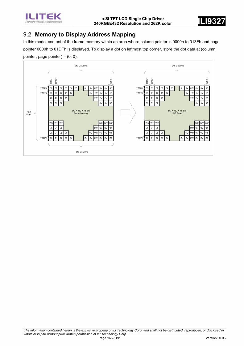
a-Si TFT LCD Single Chip Driver
240RGBx432 Resolution and 262K color ILI9327
The information contained herein is the exclusive property of ILI Technology Corp. and shall not be distributed, reproduced, or disclosed in whole or in part without prior written permission of ILI Technology Corp. Page 166 / 191 Version: 0.06
9.2. Memory to Display Address Mapping In this mode, content of the frame memory within an area where column pointer is 0000h to 013Fh and page
pointer 0000h to 01DFh is displayed. To display a dot on leftmost top corner, store the dot data at (column
pointer, page pointer) = (0, 0).
0Z0Y0X0W0V0U
1Z1Y1X1W1V
2Z2Y2X2W
3Z3Y3X
WZWYWX
XZXYXXXW
YYYXYWYV
ZZZYZXZWZVZU
YZ
Z0 Z1 Z2 Z3 Z4
Y0 Y1 Y2 Y3
X0 X1 X2
W0 W1 W2
240 X 432 X 18 BitsFrame Memory
050403020100
1413121110
23222120
323130
000h
001h
0EFh
000h
001h
1AFh
432 Lines
240 Columns
240 Columns
0Z0Y0X0W0V0U
1Z1Y1X1W1V
2Z2Y2X2W
3Z3Y3X
WZWYWX
XZXYXXXW
YYYXYWYV
ZZZYZXZWZVZU
YZ
Z0 Z1 Z2 Z3 Z4
Y0 Y1 Y2 Y3
X0 X1 X2
W0 W1 W2
240 X 432 X 18 BitsLCD Panel
050403020100
1413121110
23222120
323130
000h
001h
0EFh
000h
001h
1AFh
240 Columns

a-Si TFT LCD Single Chip Driver
240RGBx432 Resolution and 262K color ILI9327
The information contained herein is the exclusive property of ILI Technology Corp. and shall not be distributed, reproduced, or disclosed in whole or in part without prior written permission of ILI Technology Corp. Page 167 / 191 Version: 0.06
9.3. Vertical Scroll Mode There is a vertical scrolling mode, which is described by the commands “set_scroll_area”(33h) and
“set_scroll_start”(37h).
(1)Normal Display On or Partial Mode On, Vertical Scroll Off
0Z0Y0X0W0V0U
1Z1Y1X1W1V
2Z2Y2X2W
3Z3Y3X
WZWYWX
XZXYXXXW
YYYXYWYV
ZZZYZXZWZVZU
YZ
Z0 Z1 Z2 Z3 Z4
Y0 Y1 Y2 Y3
X0 X1 X2
W0 W1 W2
240 X 432 X 18 BitsFrame Memory
050403020100
1413121110
23222120
323130
000h
001h
0EFh
000h
001h
1AFh
432 Lines
240 Columns
0Z0Y0X0W0V0U
1Z1Y1X1W1V
2Z2Y2X2W
3Z3Y3X
WZWYWX
XZXYXXXW
YYYXYWYV
ZZZYZXZWZVZU
YZ
Z0 Z1 Z2 Z3 Z4
Y0 Y1 Y2 Y3
X0 X1 X2
W0 W1 W2
240 X 432 X 18 BitsLCD Panel
050403020100
1413121110
23222120
323130
000h
001h
0EFh
000h
001h
1AFh
240 Columns
(2) Vertical Scroll Mode
“set_scroll_area(33h)”and ”set_scroll_start(37h)” setting define the scroll area.
Example1: TFA=2, VSA=430, BFA=0 (set_address_mode(36h) B4=0), VSP=3
0Z0Y0X0W0V0U
1Z1Y1X1W1V
2Z2Y2X2W
3Z3Y3X
WZWYWX
XZXYXXXW
YYYXYWYV
ZZZYZXZWZVZU
YZ
Z0 Z1 Z2 Z3 Z4
Y0 Y1 Y2 Y3
X0 X1 X2
W0 W1 W2
050403020100
1413121110
23222120
323130
000h
001h
0EFh
0EEh
EDh
000h
001h
1AFh
Top fixed Area
0Z0Y0X0W0V0U
1Z1Y1X1W1V
3Z3Y3X
XZXYXXXW
YYYXYWYV
ZZZYZXZWZVZU
YZ
Z0 Z1 Z2 Z3 Z4
Y0 Y1 Y2 Y3
X0 X1 X2
050403020100
1413121110
323130
000h
001h
000h
001h
Scroll Area
Scroll pointerVSP=03h
1AEh
1ADh
2Z2Y2X2W2V2U20 21 22 23 24 25
Scroll Area
1AFh
1AEh
1ADh
34 3W
4Y4X424140 4Z
240 X 432 X 18 BitsFrame Memory
240 X 432 X 18 BitsLCD Panel
0EFh
0EEh
EDh

a-Si TFT LCD Single Chip Driver
240RGBx432 Resolution and 262K color ILI9327
The information contained herein is the exclusive property of ILI Technology Corp. and shall not be distributed, reproduced, or disclosed in whole or in part without prior written permission of ILI Technology Corp. Page 168 / 191 Version: 0.06
Example2: TFA=2,VSA=428,BFA=2 (set_address_mode(36h) B4=0), VSP=3
0Z0Y0X0W0V0U
1Z1Y1X1W1V
2Z2Y2X2W
3Z3Y3X
WZWYWX
XZXYXXXW
YYYXYWYV
ZZZYZXZWZVZU
YZ
Z0 Z1 Z2 Z3 Z4
Y0 Y1 Y2 Y3
X0 X1 X2
W0 W1 W2
050403020100
1413121110
23222120
323130
000h
001h
000h
001hTop fixed Area
0Z0Y0X0W0V0U
1Z1Y1X1W1V
3Z
XZXYXX
YYYXYWYV
ZZZYZXZWZVZU
YZ
Z0 Z1 Z2 Z3 Z4
Y0 Y1 Y2 Y3
X0 X1 X2
050403020100
1413121110
000h
001h
000h
001h
Scroll Area
Scroll pointerVSP=03h
2Z2Y2X2W20 21 22 23
Scroll Area
WYWXW0 W1 W2 WZ
Bottom fixed Area
3Y3X323130 34 3W
4Y4X424140
3Z
4Z
240 X 432 X 18 BitsFrame Memory
240 X 432 X 18 BitsLCD Panel
1AFh
1AEh
1ADh0E
Fh
0EEh
EDh
0EFh
0EEh
EDh
1AFh
1AEh
1ADh
Example3: TFA=2,VSA=428,BFA=2 (set_address_mode(36h) B4=0), VSP=5
0Z0Y0X0W0V0U
1Z1Y1X1W1V
2Z2Y2X2W
3Z3Y3X
WZWYWX
XZXYXXXW
YYYXYWYV
ZZZYZXZWZVZU
YZ
Z0 Z1 Z2 Z3 Z4
Y0 Y1 Y2 Y3
X0 X1 X2
W0 W1 W2
050403020100
1413121110
23222120
323130
000h
001h
000h
001hTop fixed Area
0Z0Y0X0W0V0U
1Z1Y1X1W1V
5Z5Y5X5W
6Z6Y6X
XZXY
YYYXYWYV
ZZZYZXZWZVZU
YZ
Z0 Z1 Z2 Z3 Z4
Y0 Y1 Y2 Y3
X0 X1
050403020100
1413121110
53525150
626160
000h
001h
000h
001h
Scroll Area
Scroll pointerVSP=03h
2Z2Y20 21
Scroll Area
Bottom fixed Area
4Z
5Z
4140
50
3Y3X30 31 32
4Y4X4W40 41 42 43
3Z
4Z
240 X 432 X 18 BitsFrame Memory
240 X 432 X 18 BitsLCD Panel
0EFh
0EEh
EDh
1AFh
1AEh
1ADh
1AFh
1AEh
1ADh
0EFh
0EEh
EDh

a-Si TFT LCD Single Chip Driver
240RGBx432 Resolution and 262K color ILI9327
The information contained herein is the exclusive property of ILI Technology Corp. and shall not be distributed, reproduced, or disclosed in whole or in part without prior written permission of ILI Technology Corp. Page 169 / 191 Version: 0.06
10. Tearing Effect Output The tearing effect output line supplies to the MCU a Panel synchronization signal. This signal can be enabled or
disabled by the set_tear_off (34h) and set_tear_on (35h) commands. The mode of the tearing effect signal is
defined by the parameter of the set_tear_on (35h) and set_tear_scanline (44h) commands.
The signal can be used by the MCU to synchronize Frame Memory Writing when displaying video images.
10.1. Tearing Effect Line Modes Mode 1 (set_tear_on, TELOM=0) , the Tearing Effect Output signal consists of V-Sync information only:
tvdl tvdh
Vertical Time Scale
tvdh = The LCD display is not updated from the Frame Memory.
tvdl = The LCD display is updated from the Frame Memory (except Invisible Line – see below).
Mode 2 (set_tear_on, TELOM=1), the tearing effect output signal consists of V-Sync and H-Sync information;
there is one V-sync and 432 H-sync pulses per field:
tvdl
V-Sync
tvdh
1st Line 480th
Line
V-SyncInvisible
Line
thdh = The LCD display is not updated from the Frame Memory.
thdl = The LCD display is updated from the Frame Memory (except Invisible Line – see above).
Bottom Line
2nd Line
1st Line
TE (mode 2)
TE (mode 1)
Note: During Sleep In Mode, the Tearing Effect Output Pin is active Low.

a-Si TFT LCD Single Chip Driver
240RGBx432 Resolution and 262K color ILI9327
The information contained herein is the exclusive property of ILI Technology Corp. and shall not be distributed, reproduced, or disclosed in whole or in part without prior written permission of ILI Technology Corp. Page 170 / 191 Version: 0.06
10.2. Tearing Effect Line Timings The tearing effect signal is described below:
tvdh
Vertical Timing
Horizontal Timing
thdl thdh
tvdl
AC characteristics of Tearing Effect Signal (Frame Rate = 60.5Hz)
Symbol Parameter Min. Max. Unit Description
tvdl Vertical timing low duration TBD ms
tvdh Vertical timing high duration TBD us
thdl Horizontal timing low duration TBD us
thdh Horizontal timing high duration TBD us
Notes:
1. The timings in Table 8.3.1 apply when MADCTL B4=0 and B4=1
2. The signal’s rise and fall times (tf, tr) are stipulated to be equal to or less than 15ns.
tr tf
80%
20%
80%
20%
The Tearing Effect Output Line is fed back to the MCU and should be used as shown below to avoid
Tearing Effect:
The Tearing Effect output line supplies to the MCU a Panel synchronization signal. This signal can be enabled or
disabled by the set_tear_off(34h), set_tear_on(35h) commands. The mode of the Tearing Effect Signal is
defined by the Parameter of the Tearing Effect Line On command. The signal can be used by the MCU to
synchronize Frame Memory Writing when displaying video images.
TEON (35h) TELOM (35h, 1st bit) TE signal Output
0 * GND 1 0 TE (Mode 1) 1 1 TE (Mode 2)

a-Si TFT LCD Single Chip Driver
240RGBx432 Resolution and 262K color ILI9327
The information contained herein is the exclusive property of ILI Technology Corp. and shall not be distributed, reproduced, or disclosed in whole or in part without prior written permission of ILI Technology Corp. Page 171 / 191 Version: 0.06
11. Sub-panel Control
TFT type sub panel timing
A. Register data transfer timing
If TFT type sub panel is selected (STN_EN=0), register setting is executed like below figure. Register data is
transferred through S_DB[8:0] in 9/8 bit type. Please refer to the MDDI section for the register address direction
to sub panel.
In this mode, data is transferred at two times. First transfer is MSB 8bit and second transfer is LSB 8bit.
HeaderRegisterAddress(1234h)
CRC
RegisterData
(0304h)
CRC
MDDI Register Access Packet
12h(MSB)
34h(MSB)
03h(MSB)
04h(MSB)S_DB[8:1]
S_CS
S_RS
S_WR
Write Index Write Parameter

a-Si TFT LCD Single Chip Driver
240RGBx432 Resolution and 262K color ILI9327
The information contained herein is the exclusive property of ILI Technology Corp. and shall not be distributed, reproduced, or disclosed in whole or in part without prior written permission of ILI Technology Corp. Page 172 / 191 Version: 0.06
B. Video data transfer timing
In TFT type sub panel, the 9/8-bit mode is selected as setting SUB_IM register.
This figure shows 9-bit sub-panel data bus with 18-bpp video data transfer.
Header Pixel Data #1(01ABCh)
CRC
1 Video Stream Packet (18-bpp)
Pixel Data #2(100FFh)
Pixel Data #3(0FF00h)
Pixel Data #4(000FFh)
Pixel Data #5(00001h)
CRC
S_DB[8:0] 00Dh(MSB)
0BCh(LSB)
080h(MSB)
0FFh(LSB)
07Fh(MSB)
100h(LSB)
000h(MSB)
0FFh(LSB)
000h(MSB)
001h(LSB)
S_CS
S_RS
S_WR
This figure shows 8-bit sub-panel data bus with 16-bpp video data transfer.
Header Pixel Data #1(1ABCh)
CRC
1 Video Stream Packet (16-bpp)
Pixel Data #2(00FFh)
Pixel Data #3(FF00h)
Pixel Data #4(01FFh)
Pixel Data #5(0001h)
CRC
S_DB[8:1] 1Ah(MSB)
BCh(LSB)
00h(MSB)
FFh(LSB)
FFh(MSB)
00h(LSB)
01h(MSB)
FFh(LSB)
00h(MSB)
01h(LSB)
S_CS
S_RS
S_WR

a-Si TFT LCD Single Chip Driver
240RGBx432 Resolution and 262K color ILI9327
The information contained herein is the exclusive property of ILI Technology Corp. and shall not be distributed, reproduced, or disclosed in whole or in part without prior written permission of ILI Technology Corp. Page 173 / 191 Version: 0.06
STN type sub panel timing
A. Register data transfer timing
This figure shows conventional type STN mode register data setting. Conventional type does not include
parameter. Instruction type is only 8bit. To use STN type, STN_EN is set to “1”. In STN type, ILI9327 controls
S_RS pin using register address[0] in register access packet. Register address[0] is “0”, then S_RS is set to “0”,
and register address[0] is “1”, S_RS is set to “1”.
HeaderRegisterAddress(0000h)
CRC
RegisterData
(0055h)
CRC
MDDI Register Access Packet Header
RegisterAddress(0000h)
CRC
RegisterData
(0012h)
CRC
Header
55h(Index)
12h(Parameter)
Write Index Write Parameter
S_DB[8:1]
S_CS
S_RS
S_WR
1 Register Access Packet 1 Register Access Packet
This type is used to include parameter. When instruction is transferred, S_RS is zero, and when parameter is
transferred, S_RS is “1”. S_RS is controlled using register address[0] of register access packet.
HeaderRegisterAddress(0000h)
CRC
RegisterData
(0055h)
CRC
MDDI Register Access Packet Header
RegisterAddress(0001h)
CRC
RegisterData
(0012h)
CRC
Header
55h(Index)
12h(Parameter)
Write Index Write Parameter
S_DB[8:1]
S_CS
S_RS
S_WR
1 Register Access Packet 1 Register Access Packet

a-Si TFT LCD Single Chip Driver
240RGBx432 Resolution and 262K color ILI9327
The information contained herein is the exclusive property of ILI Technology Corp. and shall not be distributed, reproduced, or disclosed in whole or in part without prior written permission of ILI Technology Corp. Page 174 / 191 Version: 0.06
B. Video data transfer timing
In STN mode, video data start register (like 22H in TFT mode) generally is not necessary. But some STN type
needs video data start register. If that type STN DDI is used, user has to set the register index.
This figure shows STN 9 bit mode video data transfer.
Header Pixel Data #1(01ABCh)
CRC
1 Video Stream Packet (18-bpp)
Pixel Data #2(100FFh)
Pixel Data #3(0FF00h)
Pixel Data #4(000FFh)
Pixel Data #5(00001h)
CRC
S_DB[8:0] 00Dh(MSB)
0BCh(LSB)
080h(MSB)
0FFh(LSB)
07Fh(MSB)
100h(LSB)
000h(MSB)
0FFh(LSB)
000h(MSB)
001h(LSB)
S_CS
S_RS
S_WR
This figure shows STN 8bit mode video data transfer. If STN video data is 16bit mode, data transfer is executed
during 2 times. Fist transfer is MSB 8bits, and second is LSB 8bits.
Header Pixel Data #1(1ABCh)
CRC
1 Video Stream Packet (16-bpp)
Pixel Data #2(00FFh)
Pixel Data #3(FF00h)
Pixel Data #4(01FFh)
Pixel Data #5(0001h)
CRC
S_DB[8:1] 1Ah(MSB)
BCh(LSB)
00h(MSB)
FFh(LSB)
FFh(MSB)
00h(LSB)
01h(MSB)
FFh(LSB)
00h(MSB)
01h(LSB)
S_CS
S_RS
S_WR

a-Si TFT LCD Single Chip Driver
240RGBx432 Resolution and 262K color ILI9327
The information contained herein is the exclusive property of ILI Technology Corp. and shall not be distributed, reproduced, or disclosed in whole or in part without prior written permission of ILI Technology Corp. Page 175 / 191 Version: 0.06
12. NV Memory Programming Flow Start
Reset ILI9327
CheckPGM_CNT (RE2h P1)
= 2b’11 (VCM)
Supply External Power7.0Volt to DDVDH pin
Wait 50ms
Cut Off External7.0V Power
Reset
End
Y
Set Control RegisterRE1h P1 = 0x10 (VCM)
RE1h P1 = 0x20 (ID)
Set NV Programming Value
RE0h P1 = xx
Set ID KeyRE3h P1 = 0xAARE3h P2 = 0x55
N
Set RE7h P1 = 0x0ASet RE7h P2 = 0x7F
Confirm OTP valueRead RE2h P1, P2 (VCM)
Read RA1h P1 (ID)

a-Si TFT LCD Single Chip Driver
240RGBx432 Resolution and 262K color ILI9327
The information contained herein is the exclusive property of ILI Technology Corp. and shall not be distributed, reproduced, or disclosed in whole or in part without prior written permission of ILI Technology Corp. Page 176 / 191 Version: 0.06
13. Gamma Correction ILI9327 incorporates the γ-correction function to display 262,144 colors for the LCD panel. The γ-correction is
performed with 3 groups of registers determining eight reference grayscale levels, which are gradient
adjustment, amplitude adjustment and fine-adjustment registers for positive and negative polarities, to make
ILI9327 available with liquid crystal panels of various characteristics.

a-Si TFT LCD Single Chip Driver
240RGBx432 Resolution and 262K color ILI9327
The information contained herein is the exclusive property of ILI Technology Corp. and shall not be distributed, reproduced, or disclosed in whole or in part without prior written permission of ILI Technology Corp. Page 177 / 191 Version: 0.06
VgP79
VP1VP2VP3VP4VP5VP6VP7VP8
RP1RP2RP3RP4RP5RP6RP7
RP15
VP25VP26VP27VP28VP29VP30VP31VP32
RP24RP25RP26RP27RP28RP29RP30
RP23
VP33VP34VP35VP36VP37VP38VP39VP40
RP31
RP46
RP47
8 to
1
Sele
ctio
n8
to 1
Se
lect
ion
VP9VP10VP11VP12VP13VP14VP15VP16
RP8RP9
RP10RP11RP12RP13RP14
VgP70
VgP63
VP17VP18VP19VP20VP21VP22VP23VP24
RP16RP17RP18RP19RP20RP21RP22
REP00 ~ 15R
PKP0[2:0]
PKP1[2:0]
8 to
1
Sele
ctio
n
VgP51
PKP2[2:0]
8 to
1
Sele
ctio
n
VgP28
PKP3[2:0]
RCP00 ~ 28R
5R5R
{4Rx7=28R
{Rx7=7R
{
{{
VREP0[3:0]
PRP0[2:0]
PRP1[2:0]
VRP1[4:0]
RP33RP34RP35RP36RP37RP38
RP32
8 to
1
Sele
ctio
n
VgP16
PKP4[2:0]
VP41VP42VP43VP44VP45VP46VP47VP48
RP40RP41RP42RP43RP44RP45
RP39
8 to
1
Sele
ctio
n
VgP9
PKP5[2:0]
VgP4
5R
8R
ROP10 ~ 31R
VREG1OUT
VGS
RP0
RCP10 ~ 28R
1uF/6VREP1
0 ~ 15R VREP1[3:0]
ROP00 ~ 30R VRP0[3:0] VgP75
5R
Rx7=7R
16R
{Rx7=7R
5R
Rx7=7R
4Rx7=28R
VREP2[3:0]REP20 ~ 15R
VgP0
VgN79
VN1VN2VN3VN4VN5VN6VN7VN8
RN1RN2RN3RN4RN5RN6RN7
RP15
VN25VN26VN27VN28VN29VN30VN31VN32
RN24RN25RN26RN27RN28RN29RN30
RN23
VN33VN34VN35VN36VN37VN38VN39VN40
RN31
RN46
RN47
8 to
1
Sele
ctio
n8
to 1
Se
lect
ion
VN9VN10VN11VN12VN13VN14VN15VN16
RN8RN9
RN10RN11RN12RN13RN14
VgN70
VgN63
VN17VN18VN19VN20VN21VN22VN23VN24
RN16RN17RN18RN19RN20RN21RN22
REN00 ~ 15R
PKN0[2:0]
PKN1[2:0]
8 to
1
Sele
ctio
n
VgN51
PKN2[2:0]
8 to
1
Sele
ctio
n
VgN28
PKN3[2:0]
RCN00 ~ 28R
5R5R
{4Rx7=28R
{Rx7=7R
{
{{
PRN0[2:0]
PRN1[2:0]
VRN1[4:0]
RN33RN34RN35RN36RN37RN38
RN32
8 to
1
Sele
ctio
n
VgN16
PKN4[2:0]
VN41VN42VN43VN44VN45VN46VN47VN48
RN40RN41RN42RN43RN44RN45
RN39
8 to
1
Sele
ctio
n
VgN9
PKN5[2:0]
VgN4
5R
8R
RON10 ~ 31R
RN0
RCN10 ~ 28R
REN10 ~ 15R
RON00 ~ 30R VRN0[3:0] VgN75
5R
Rx7=7R
16R
{Rx7=7R
5R
Rx7=7R
4Rx7=28R
REN20 ~ 15R
VgN0
VREN0[3:0]
VREN1[3:0]
VREN2[3:0]
Gamma63
Gamma62
Gamma55
Gamma43
Gamma20
Gamma8
Gamma1
Gamma0
Gamma63
Gamma62
Gamma55
Gamma43
Gamma20
Gamma8
Gamma1
Gamma0
Figure 1 Grayscale Voltage Adjustment

a-Si TFT LCD Single Chip Driver
240RGBx432 Resolution and 262K color ILI9327
The information contained herein is the exclusive property of ILI Technology Corp. and shall not be distributed, reproduced, or disclosed in whole or in part without prior written permission of ILI Technology Corp. Page 178 / 191 Version: 0.06
8 to
1
sele
ctio
n
8 to
1
sele
ctio
n
8 to
1
sele
ctio
n
8 to
1
sele
ctio
n
8 to
1
sele
ctio
n
8 to
1
sele
ctio
n
PRP/N0
Gradient Adjustment Register
PRP/N1 VRP/N0
Amplitude Adjustment Register
VRP/N1PKP/N5
Fine Adjustment Registers ( 6 x 3 bits)
VREG1OUT
VGS
PKP/N4 PKP/N3 PKP/ N2 PKP/N1 PKP/N0 VREG1 OUT
V75
VGS
VgP4/ VgN4
VgP9/VgN9
VgP16/ VgN16
VgP28/ VgN28
VgP75/ VgN75
VgP51/ VgN51
VgP70/ VgN70
VgP63/ VgN63
VgP0/ VgN0
VgP79/ VgN79
VREP/N0
EEMAdjustment Register
VREP/N1 VREP/N2
V79V78
……
……
V70
……
V63
……
……
……
……
……
V51
V28
V16
V9
V4
……
V0
1. Gradient adjustment registers
The gradient adjustment registers are used to adjust the gradient of the curve representing the relationship
between the grayscale and the grayscale reference voltage level. To adjust the gradient, the resistance values
of variable resistors in the middle of the ladder resistor are adjusted by registers PRP0[2:0]/PRN0[2:0],
PRP1[2:0]/PRN1[2:0]. The registers consist of positive and negative polarity registers, allowing asymmetric
drive.
2. Amplitude adjustment registers
The amplitude adjustment registers, VRP0[3:0]/VRN0[3:0], VRP1[4:0]/VRN1[4:0], are used to adjust the

a-Si TFT LCD Single Chip Driver
240RGBx432 Resolution and 262K color ILI9327
The information contained herein is the exclusive property of ILI Technology Corp. and shall not be distributed, reproduced, or disclosed in whole or in part without prior written permission of ILI Technology Corp. Page 179 / 191 Version: 0.06
amplitude of grayscale voltages. To adjust the amplitude, the resistance values of variable resistors at the top
and bottom of the ladder resistor are adjusted. Same as the gradient registers, the amplitude adjustment
registers consist of positive and negative polarity registers.
3. Fine adjustment registers
The fine adjustment registers are used to fine-adjust grayscale voltage levels. To fine-adjust grayscale voltage
levels, fine adjustment registers adjust the reference voltage levels, 8 levels for each register generated from the
ladder resistor, in respective 8-to-1 selectors. Same with other registers, the fine adjustment registers consist of
positive and negative polarity registers.
Gradient adjustment
Gra
ysca
le v
olta
ge
Amplitude adjustment
Gra
ysca
le v
olta
ge
Fine adjustment
Gra
ysca
le v
olta
ge
Figure 2 Gamma Curve Adjustment
Register Groups Positive Polarity Negative Polarity Description Gradient adjustment
PRP0 [2:0] PRN0 [2:0] Variable resistor VRCP0, VRCN0 PRP1 [2:0] PRN1 [2:0] Variable resistor VRCP1, VRCN1
Amplitude adjustment
VRP0 [3:0] VRN0 [3:0] Variable resistor VROP0, VRON0 VRP1 [4:0] VRN1 [4:0] Variable resistor VROP1, VRON1
Fine adjustment
KP0 [2:0] KN0 [2:0] 8-to-1 selector (voltage level of grayscale 1) KP1 [2:0] KN1 [2:0] 8-to-1 selector (voltage level of grayscale 8) KP2 [2:0] KN2 [2:0] 8-to-1 selector (voltage level of grayscale 20) KP3 [2:0] KN3 [2:0] 8-to-1 selector (voltage level of grayscale 43) KP4 [2:0] KN4 [2:0] 8-to-1 selector (voltage level of grayscale 55) KP5 [2:0] KN5 [2:0] 8-to-1 selector (voltage level of grayscale 62)
Ladder resistors and 8-to-1 selector Block configuration
The reference voltage generating block consists of two ladder resistor units including variable resistors and
8-to-1 selectors. Each 8-to-1 selector selects one of the 8 voltage levels generated from the ladder resistor unit
to output as a grayscale reference voltage. Both variable resistors and 8-to-1 selectors are controlled according
to the γ-correction registers. This unit has pins to connect a volume resistor externally to compensate
differences in various characteristics of panels.
Variable resistors
ILI9327 uses variable resistors of the following three purposes: gradient adjustment (VRCP(N)0/VRCP(N)1);
amplitude adjustment (1) (VROP(N)0); and the amplitude adjustment (2) (VROP(N)1). The resistance values of
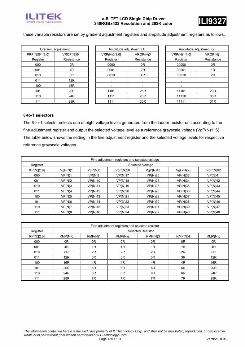
a-Si TFT LCD Single Chip Driver
240RGBx432 Resolution and 262K color ILI9327
The information contained herein is the exclusive property of ILI Technology Corp. and shall not be distributed, reproduced, or disclosed in whole or in part without prior written permission of ILI Technology Corp. Page 180 / 191 Version: 0.06
these variable resistors are set by gradient adjustment registers and amplitude adjustment registers as follows.
Gradient adjustment Amplitude adjustment (1) Amplitude adjustment (2) PRP(N)0/1[2:0]
Register VRCP(N)0/1 Resistance
VRP(N)0[3:0] Register
VROP(N)0 Resistance
VRP(N)1[4:0] Register
VROP(N)1 Resistance
000 0R 0000 0R 00000 0R 001 4R 0001 2R 00001 1R 010 8R 0010 4R 00010 2R 011 12R : : : : 100 16R : : : : 101 20R 1101 26R 11101 29R 110 24R 1111 28R 11110 30R 111 28R 1111 30R 11111 31R
8-to-1 selectors
The 8-to-1 selector selects one of eight voltage levels generated from the ladder resistor unit according to the
fine adjustment register and output the selected voltage level as a reference grayscale voltage (VgP(N)1~6).
The table below shows the setting in the fine adjustment register and the selected voltage levels for respective
reference grayscale voltages.
Fine adjustment registers and selected voltage Register Selected Voltage
KP(N)[2:0] VgP(N)1 VgP(N)8 VgP(N)20 VgP(N)43 VgP(N)55 VgP(N)62 000 VP(N)1 VP(N)9 VP(N)17 VP(N)25 VP(N)33 VP(N)41 001 VP(N)2 VP(N)10 VP(N)18 VP(N)26 VP(N)34 VP(N)42 010 VP(N)3 VP(N)11 VP(N)19 VP(N)27 VP(N)35 VP(N)43 011 VP(N)4 VP(N)12 VP(N)20 VP(N)28 VP(N)36 VP(N)44 100 VP(N)5 VP(N)13 VP(N)21 VP(N)29 VP(N)37 VP(N)45 101 VP(N)6 VP(N)14 VP(N)22 VP(N)30 VP(N)38 VP(N)46 110 VP(N)7 VP(N)15 VP(N)23 VP(N)31 VP(N)39 VP(N)47 111 VP(N)8 VP(N)16 VP(N)24 VP(N)32 VP(N)40 VP(N)48
Fine adjustment registers and selected resistor Register Selected Resistor
KP(N)[2:0] RMP(N)0 RMP(N)1 RMP(N)2 RMP(N)3 RMP(N)4 RMP(N)5 000 0R 0R 0R 0R 0R 0R 001 4R 1R 1R 1R 1R 4R 010 8R 2R 2R 2R 2R 8R 011 12R 3R 3R 3R 3R 12R 100 16R 4R 4R 4R 4R 16R 101 20R 5R 5R 5R 5R 20R 110 24R 6R 6R 6R 6R 24R 111 28R 7R 7R 7R 7R 28R

a-Si TFT LCD Single Chip Driver
240RGBx432 Resolution and 262K color ILI9327
The information contained herein is the exclusive property of ILI Technology Corp. and shall not be distributed, reproduced, or disclosed in whole or in part without prior written permission of ILI Technology Corp. Page 181 / 191 Version: 0.06
VP 1VP 2VP 3VP 4
VP 5VP 6
VP 7VP 8
RP1
RP2
RP3
RP4
RP5
RP6
RP7
VgP1=VP3
KP0[2:0]=010
{4Rx7=28R
{RMP0=8R
Figure 3 Example of RMP(N)0~5 definition
Code Positive polarity output voltage Negative polarity output voltage
4Fh VP79 (VgP79) VN79 (VgN79) 4Eh VP78 (VP75+(VP79-VP75)*(48/64)) VN78 (VN75+(VN79-VN75)*(48/64)) 4Dh VP77 (VP75+(VP79-VP75)*(32/64)) VN77 (VN75+(VN79-VN75)*(32/64)) 4Ch VP76 (VP75+(VP79-VP75)*(16/64)) VN76 (VN75+(VN79-VN75)*(16/64)) 4Bh VP75 (VgP75) VN75 (VgN75) 4Ah VP74 (VP70+(VP75-VP70)*(36/45)) VN74 (VN70+(VN75-VN70)*(36/45)) 49h VP73 (VP70+(VP75-VP70)*(27/45)) VN73 (VN70+(VN75-VN70)*(27/45)) 48h VP72 (VP70+(VP75-VP70)*(18/45)) VN72 (VN70+(VN75-VN70)*(18/45)) 47h VP71 (VP70+(VP75-VP70)*(9/45)) VN71 (VN70+(VN75-VN70)*(9/45)) 46h VP70 (VgP70) VN70 (VgN70) 45h VP69 (VP63+(VP70-VP63)*(30/48)) VN69 (VN63+(VN70-VN63)*(30/48)) 44h VP68 (VP63+(VP70-VP63)*(23/48)) VN68 (VN63+(VN70-VN63)*(23/48)) 43h VP67 (VP63+(VP70-VP63)*(16/48)) VN67 (VN63+(VN70-VN63)*(16/48)) 42h VP66 (VP63+(VP70-VP63)*(12/48)) VN66 (VN63+(VN70-VN63)*(12/48)) 41h VP65 (VP63+(VP70-VP63)*(8/48)) VN65 (VN63+(VN70-VN63)*(8/48)) 40h VP64 (VP63+(VP70-VP63)*(4/48)) VN64 (VN63+(VN70-VN63)*(4/48)) 3Fh VP63 (VgP63) VN63 (VgN63) 3Eh VP62 (VP51+(VP63-VP51)*(22/24)) VN62 (VN51+(VN63-VN51)*(22/24)) 3Dh VP61 (VP51+(VP63-VP51)*(20/24)) VN61 (VN51+(VN63-VN51)*(20/24)) 3Ch VP60 (VP51+(VP63-VP51)*(18/24)) VN60 (VN51+(VN63-VN51)*(18/24)) 3Bh VP59 (VP51+(VP63-VP51)*(16/24)) VN59 (VN51+(VN63-VN51)*(16/24)) 3Ah VP58 (VP51+(VP63-VP51)*(14/24)) VN58 (VN51+(VN63-VN51)*(14/24)) 39h VP57 (VP51+(VP63-VP51)*(12/24)) VN57 (VN51+(VN63-VN51)*(12/24)) 38h VP56 (VP51+(VP63-VP51)*(10/24)) VN56 (VN51+(VN63-VN51)*(10/24)) 37h VP55 (VP51+(VP63-VP51)*(8/24)) VN55 (VN51+(VN63-VN51)*(8/24)) 36h VP54 (VP51+(VP63-VP51)*(6/24)) VN54 (VN51+(VN63-VN51)*(6/24)) 35h VP53 (VP51+(VP63-VP51)*(4/24)) VN53 (VN51+(VN63-VN51)*(4/24)) 34h VP52 (VP51+(VP63-VP51)*(2/24)) VN52 (VN51+(VN63-VN51)*(2/24)) 33h VP51 (VgP51) VN51 (VgN51) 32h VP50 (VP28+(VP51-VP28)*(22/23)) VN50 (VN28+(VN51-VN28)*(22/23)) 31h VP49 (VP28+(VP51-VP28)*(21/23)) VN49 (VN28+(VN51-VN28)*(21/23)) 30h VP48 (VP28+(VP51-VP28)*(20/23)) VN48 (VN28+(VN51-VN28)*(20/23))
2Fh VP47 (VP28+(VP51-VP28)*(19/23)) VN47 (VN28+(VN51-VN28)*(19/23)) 2Eh VP46 (VP28+(VP51-VP28)*(18/23)) VN46 (VN28+(VN51-VN28)*(18/23)) 2Dh VP45 (VP28+(VP51-VP28)*(17/23)) VN45 (VN28+(VN51-VN28)*(17/23)) 2Ch VP44 (VP28+(VP51-VP28)*(16/23)) VN44 (VN28+(VN51-VN28)*(16/23)) 2Bh VP43 (VP28+(VP51-VP28)*(15/23)) VN43 (VN28+(VN51-VN28)*(15/23)) 2Ah VP42 (VP28+(VP51-VP28)*(14/23)) VN42 (VN28+(VN51-VN28)*(14/23)) 29h VP41 (VP28+(VP51-VP28)*(13/23)) VN41 (VN28+(VN51-VN28)*(13/23)) 28h VP40 (VP28+(VP51-VP28)*(12/23)) VN40 (VN28+(VN51-VN28)*(12/23)) 27h VP39 (VP28+(VP51-VP28)*(11/23)) VN39 (VN28+(VN51-VN28)*(11/23)) 26h VP38 (VP28+(VP51-VP28)*(10/23)) VN38 (VN28+(VN51-VN28)*(10/23)) 25h VP37 (VP28+(VP51-VP28)*(9/23)) VN37 (VN28+(VN51-VN28)*(9/23))

a-Si TFT LCD Single Chip Driver
240RGBx432 Resolution and 262K color ILI9327
The information contained herein is the exclusive property of ILI Technology Corp. and shall not be distributed, reproduced, or disclosed in whole or in part without prior written permission of ILI Technology Corp. Page 182 / 191 Version: 0.06
24h VP36 (VP28+(VP51-VP28)*(8/23)) VN36 (VN28+(VN51-VN28)*(8/23)) 23h VP35 (VP28+(VP51-VP28)*(7/23)) VN35 (VN28+(VN51-VN28)*(7/23)) 22h VP34 (VP28+(VP51-VP28)*(6/23)) VN34 (VN28+(VN51-VN28)*(6/23)) 21h VP33 (VP28+(VP51-VP28)*(5/23)) VN33 (VN28+(VN51-VN28)*(5/23)) 20h VP32 (VP28+(VP51-VP28)*(4/23)) VN32 (VN28+(VN51-VN28)*(4/23)) 1Fh VP31 (VP28+(VP51-VP28)*(3/23)) VN31 (VN28+(VN51-VN28)*(3/23)) 1Eh VP30 (VP28+(VP51-VP28)*(2/23)) VN30 (VN28+(VN51-VN28)*(2/23)) 1Dh VP29 (VP28+(VP51-VP28)*(1/23)) VN29 (VN28+(VN51-VN28)*(1/23)) 1Ch VP28 (VgP28) VN28 (VgN28) 1Bh VP27 (VP16+(VP28-VP16)*(22/24)) VN27 (VN16+(VN28-VN16)*(22/24)) 1Ah VP26 (VP16+(VP28-VP16)*(20/24)) VN26 (VN16+(VN28-VN16)*(20/24)) 19h VP25 (VP16+(VP28-VP16)*(18/24)) VN25 (VN16+(VN28-VN16)*(18/24)) 18h VP24 (VP16+(VP28-VP16)*(16/24)) VN24 (VN16+(VN28-VN16)*(16/24)) 17h VP23 (VP16+(VP28-VP16)*(14/24)) VN23 (VN16+(VN28-VN16)*(14/24)) 16h VP22 (VP16+(VP28-VP16)*(12/24)) VN22 (VN16+(VN28-VN16)*(12/24)) 15h VP21 (VP16+(VP28-VP16)*(10/24)) VN21 (VN16+(VN28-VN16)*(10/24)) 14h VP20 (VP16+(VP28-VP16)*(8/24)) VN20 (VN16+(VN28-VN16)*(8/24)) 13h VP19 (VP16+(VP28-VP16)*(6/24)) VN19 (VN16+(VN28-VN16)*(6/24)) 12h VP18 (VP16+(VP28-VP16)*(4/24)) VN18 (VN16+(VN28-VN16)*(4/24)) 11h VP17 (VP16+(VP28-VP16)*(2/24)) VN17 (VN16+(VN28-VN16)*(2/24)) 10h VP16 (VgP16) VN16 (VgN16) 0Fh VP15 (VP9+(VP16-VP9)*(44/48)) VN15 (VN9+(VN16-VN9)*(44/48)) 0Eh VP14 (VP9+(VP16-VP9)*(40/48)) VN14 (VN9+(VN16-VN9)*(40/48)) 0Dh VP13 (VP9+(VP16-VP9)*(36/48)) VN13 (VN9+(VN16-VN9)*(36/48)) 0Ch VP12 (VP9+(VP16-VP9)*(32/48)) VN12 (VN9+(VN16-VN9)*(32/48)) 0Bh VP11 (VP9+(VP16-VP9)*(25/48)) VN11 (VN9+(VN16-VN9)*(25/48)) 0Ah VP10 (VP9+(VP16-VP9)*(18/48)) VN10 (VN9+(VN16-VN9)*(18/48)) 09h VP9 (VgP9) VN9 (VgN9) 08h VP8 (VP4+(VP9-VP4)*(36/45)) VN8 (VN4+(VN9-VN4)*(36/45)) 07h VP7 (VP4+(VP9-VP4)*(27/45)) VN7 (VN4+(VN9-VN4)*(27/45)) 06h VP6 (VP4+(VP9-VP4)*(18/45)) VN6 (VN4+(VN9-VN4)*(18/45)) 05h VP5 (VP4+(VP9-VP4)*(9/45)) VN5 (VN4+(VN9-VN4)*(9/45)) 04h VP4 (VgP4) VN4 (VgN4) 03h VP3 (VP0+(VP4-VP0)*(48/64)) VN3 (VN0+(VN4-VN0)*(48/64)) 02h VP2 (VP0+(VP4-VP0)*(32/64)) VN2 (VN0+(VN4-VN0)*(32/64)) 01h VP1 (VP0+(VP4-VP0)*(16/64)) VN1 (VN0+(VN4-VN0)*(16/64)) 00h VP0 (VgP0) VN0 (VgN0)
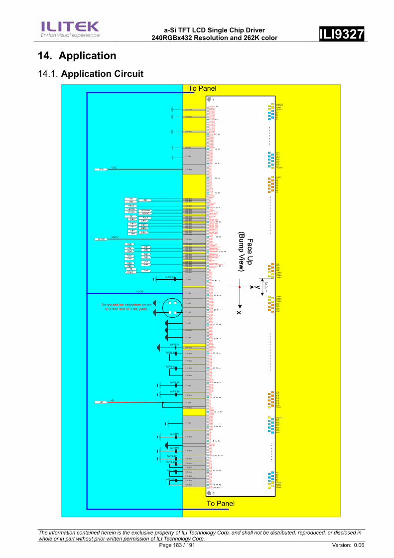
a-Si TFT LCD Single Chip Driver
240RGBx432 Resolution and 262K color ILI9327
The information contained herein is the exclusive property of ILI Technology Corp. and shall not be distributed, reproduced, or disclosed in whole or in part without prior written permission of ILI Technology Corp. Page 183 / 191 Version: 0.06
14. Application 14.1. Application Circuit
< 60 ohm
< 5 ohm
< 10 ohm
< 60 ohm
< 60 ohm< 60 ohm< 60 ohm
< 60 ohm
< 60 ohm< 60 ohm
< 60 ohm< 60 ohm< 60 ohm< 60 ohm
< 60 ohm< 60 ohm
< 60 ohm< 60 ohm< 60 ohm< 60 ohm< 60 ohm< 60 ohm< 60 ohm
< 60 ohm< 60 ohm< 60 ohm< 60 ohm
< 60 ohm< 60 ohm< 60 ohm< 60 ohm
< 60 ohm
< 60 ohm< 60 ohm< 60 ohm< 60 ohm
< 60 ohm< 60 ohm
< 10 ohm
< 10 ohm
< 10 ohm
< 5 ohm
< 5 ohm
< 10 ohm
< 20 ohm
< 20 ohm
< 20 ohm
< 20 ohm
< 20 ohm
< 20 ohm
< 5 ohm
< 5 ohm
< 5 ohm
< 60 ohm
< 10 ohm
<60 ohm
< 60 ohm
< 20 ohm
< 10 ohm
< 60 ohm
< 5 ohm
< 10 ohm
< 10 ohm
< 5 ohm
< 60 ohm
< 5 ohm
< 5 ohm
< 60 ohm
TE
CSXDCXWRX
RDX
DINDOUT
DB0 DB1DB2
DB3DB4 DB5DB6 DB7DB8
DB9 DB10DB11
DB12DB13
DB14DB15DB16
DB17 PCLKDEHSYNC
IM0
To Panel
To Panel
Face Up
(Bump View
)
DUMMYDUMMYDUMMYDUMMYS361S362S363S364S365S366
x
y
S356S357S358S359S360DUMMYDUMMYDUMMYDUMMY
……
……
……
……
.
G12G10G8G6G4G2VGLDMY1DUMMYDUMMYDUMMY
VGLDMY2G432G430G428G426G424G422G420G418G416
S712S713S714S715S716S717S718S719S720DUMMY
……
……
DUMMYR4DUMMYR3DUMMYVGLDMY4G1G3G5G7G9G11
G415G417G419G421G423G425G427G429G431VGLDMY3
DUMMYS1S2S3S4S5S6S7S8S9
……
……
……
……
……
……
.
DUMMYR1 DUMMYR2 GNDDUMTESTO[1]TESTO[2]TESTO[3]TESTO[4]GNDDUMTESTO[5]TESTO[6]TESTO[7] TESTO[8] TESTO[9] TESTO[10]TESTO[11]TESTO[12]TESTO[13]GNDDUM TESTO[14]TESTO[15]DUMMYDUMMYDUMMYDUMMYDUMMYDUMMYDUMMYDUMMYGNDDUM DGND DGNDDGNDDGNDDGNDDGNDDGNDDGNDDGNDDGNDDGNDVCC VCC VCC VCC VCC VCC VCC TS[8]TS[7]TS[6]TS[5]TS[4]TS[3]TS[2]TS[1]TS[0]TEST5TEST4TEST3TEST2TEST1 GNDDUM DUMMY IM2 IM1 IM0 IOVCCDUMDUMMY RESX GNDDUM LEDON LEDPWM VSYNC (S_CS) HSYNC (S_RS) IOVCCDUM DE (S_WR) PCLK DB[17] (S_DB[8])DB[16] (S_DB[7])DGNDDUM DB[15] (S_DB[6])DB[14] (S_DB[5])DB[13] (S_DB[4])DB[12] (S_DB[3])DGNDDUMDB[11] (S_DB[2])DB[10] (S_DB[1])DB[9] (S_DB[0]) IOVCCIOVCC
VDD VDD VDD DUMMYVCOM VCOM VCOM VCOM VCOM VCOM VCOM VCOM VCOMHVCOMHVCOMHVCOMHVCOMHVCOMHVCOMLVCOMLVCOMLVCOMLVCOMLVCOMLAGND AGND AGND AGND AGND AGND AGNDAGNDAGNDVGS AGNDAGNDAGNDAGNDAGNDAGNDAGND AGND AGND DUMMYDUMMYVREG1OUTDUMMYC11A C11A C11A C11A C11A C11B C11B C11B C11B C11B C12A C12A C12A C12A C12A C12B C12B C12B C12B C12B DDVDHDDVDHDDVDHDDVDHDDVDHDDVDHDDVDHDDVDHDDVDHVCI1 VCI1 VCI1 VCI1 VCI VCI VCI VCI VCI VCI VCILVLDUMMYDUMMYDUMMY
VGL GNDDUMGNDDUMVGH VGH VGH VGH VGH VGH GNDDUM
DUMMYDUMMYAGND AGND AGND AGND AGND AGND AGND AGND AGNDAGNDVGL VGL VGL VGL VGL VGL VGL VGL
110
2030
4050
6070
8090
100
110120
130
140
150
160
170
180
190
200
210
220
230
240250
260
262
VCL VCL VCL C13AC13AC13AC13BC13BC13BC21AC21AC21AC21BC21BC21BC22AC22AC22AC22BC22BC22BDUMMY
840um
A1A2
GNDDUMTE DIN DOUT VDD VDD VDD VDD VDD VDD
GNDDUM DB[3]/MDDIGND DB[2]/MDDI_STB_P DB[1]/MDDIGND DB[0] GNDDUM CSX DCX/MDDIGND WRX/SCL/MDDI_STB_MRDX/MDDIGND
IOVCC IOVCC IOVCC IOVCC DB[8]/MDDIGND DGNDDUM DB[7]/MDDI_DATA_PDB[6]/MDDIGND DB[5]/MDDI_DATA_MDB[4]/MDDIGND
1uF/25V
1uF/10V
1uF/10V
1uF/6.3V
1uF/6.3V
1uF/25V
1uF/6.3V
1uF/6.3V
1uF/6.3V
1uF/6.3V
1uF/6.3V
1uF/6.3V
IM2 IM1
RESXLEDONVSYNC LEDPWM
VCOM
VCI
IOVCC
VCCVCC
IOVCC
VCI
Do not add the capacitors on the VCOMH and VCOML pads.

a-Si TFT LCD Single Chip Driver
240RGBx432 Resolution and 262K color ILI9327
The information contained herein is the exclusive property of ILI Technology Corp. and shall not be distributed, reproduced, or disclosed in whole or in part without prior written permission of ILI Technology Corp. Page 184 / 191 Version: 0.06
14.2. Power Supply Configuration
Power Supply ON (VCC, VCI, IOVCC)VCI IOVCC
GNDVCI IOVCC
or VCI, IOVCC any sequence
Power On Reset
Registers setting before power supply
startup
1ms or more
10ms or moreOscillator
Stabilizing time
Set exit_sleep_mode (R11h)
command
Power supply operation Step-up circuits start to boost
Set display register
40ms or more Step-up circuit stabilizing time
Write Memory Data
Set_display_on(R29h)
Power ON Sequence
Normal Display
Set_display_off(R28h)
Enter_sleep_mode(R10h)
Power Supply OFF (VCC, VCI, IOVCC)
VCIIOVCC
GNDIOVCC VCI
Or IOVCC, VCI any sequence
Power OFF Sequence
Power supply operation setting Set BT[2:0], VC[2:0], VRH[4:0], PON, VCIRESet SELVCM, VCM[6:0], VDV[4:0]Set Apn[2:0], DCnn[2:0]
Display Environment Setting1. set normal/partial mode2. set line/fame inversion3. set interface pixel format4. set idle mode on/off5. set row/column direction6. set row/column address7. etc.
More than 120ms after reset
Wait for more than 2 frame

a-Si TFT LCD Single Chip Driver
240RGBx432 Resolution and 262K color ILI9327
The information contained herein is the exclusive property of ILI Technology Corp. and shall not be distributed, reproduced, or disclosed in whole or in part without prior written permission of ILI Technology Corp. Page 185 / 191 Version: 0.06
15. Electrical Characteristics 15.1. Absolute Maximum Ratings The absolute maximum rating is listed on following table. When ILI9327 is used out of the absolute maximum
ratings, ILI9327 may be permanently damaged. To use the ILI9327 within the following electrical characteristics
limit is strongly recommended for normal operation. If these electrical characteristic conditions are exceeded
during normal operation, the ILI9327 will malfunction and cause poor reliability.
Item Symbol Unit Value NotePower supply voltage IOVCC V -0.3 ~ + 4.6 1,2 Power supply voltage VCI - GND V -0.3 ~ + 4.6 1,3 Power supply voltage DDVDH - GND V -0.3 ~ + 6.0 1,4 Power supply voltage GND -VCL V -0.3 ~ + 4.6 1 Power supply voltage DDVDH - VCL V -0.3 ~ + 9.0 1,5 Power supply voltage VGH - GND V -0.3 ~ + 18 1,6 Power supply voltage GND - VGL V -0.3 ~ + 18 1,7 Power supply voltage VGH - VGL V 0.3 ~ + 30 Input voltage Vt V -0.3 ~ IOVCC+ 0.3 1 Operating temperature Topr °C -40 ~ + 85 8, 9 Storage temperature Tstg °C -55 ~ + 110 8, 9 Notes: 1. GND must be maintained 2. (High) (VCC = VCC) ≥ GND (Low), (High) IOVCC ≥ GND (Low). 3. Make sure (High) VCI ≥ GND (Low). 4. Make sure (High) DDVDH ≥ GND (Low). 5. Make sure (High) DDVDH ≥ VCL (Low). 6. Make sure (High) VGH ≥ GND (Low). 7. Make sure (High) GND ≥ VGL (Low). 8. For die and wafer products, specified up to 85°C. 9. This temperature specifications apply to the TCP package

a-Si TFT LCD Single Chip Driver
240RGBx432 Resolution and 262K color ILI9327
The information contained herein is the exclusive property of ILI Technology Corp. and shall not be distributed, reproduced, or disclosed in whole or in part without prior written permission of ILI Technology Corp. Page 186 / 191 Version: 0.06
15.2. DC Characteristics (VCC=VCI=2.50 ~ 3.3V, IOVCC = 1.65 ~ 3.3V, Ta= -40 ~ 85 °C)
Parameter Symbol Condition Min. Typ. Max. UnitAnalog Power Supply Voltage VCI Analog Operation Voltage 2.5 2.8 3.6 V I/O pin Power Supply Voltage IOVCC I/O pin Operation Voltage 1.65 2.8 3.6 V Input high voltage VIH IOVCC = 1.65V ~ 3.3V 0.7*IOVCC - IOVCC V Input low voltage VIL IOVCC = 1.65V ~ 3.3V 0.0 - 0.3*IOVCC V Output high voltage VOH Iout = -0.1 mA 0.8*IOVCC - IOVCC V Output low voltage VOL Iout = +0.1 mA 0.0 - 0.2*IOVCC V I/O leakage current ILI Vin=0 ~ IOVCC -0.1 0.1 uA Current consumption during normal operation (VCC, VCI, IOVCC)
IOP VCC=VCI=IOVCC=2.8V,Ta=25°C, GRAM data=0000h, Frame rate=60Hz, line inversion
- TBD - mA
Current consumption during standby operation (VCC, VCI, IOVCC)
IST VCC=VCI=IOVCC=2.8V, Ta=25°C, CPU interface
- 50 TBD uA
LCD Drive Power Supply Current (DDVDH-GND)
ILCD VCC=VCI=IOVCC=2.8V,Ta=25°C, GRAM data=0000h, Frame rate=60Hz, line inversion
7.0 - mA
LCD Drive voltage DDVDH 4.5 6 VoltOutput deviation voltage IDEV 20 mVOutput offset voltage IOFFSET Note1 35 mV
Note 1: The Max. value is between with measure point and gamma setting value.

a-Si TFT LCD Single Chip Driver
240RGBx432 Resolution and 262K color ILI9327
The information contained herein is the exclusive property of ILI Technology Corp. and shall not be distributed, reproduced, or disclosed in whole or in part without prior written permission of ILI Technology Corp. Page 187 / 191 Version: 0.06
15.3. AC Characteristics
15.3.1. DBI Type B (18/16/9/8 bit) Interface Timing Characteristics
tast
D/CX
CSX
WRX
D[17:0](Write)
RDX
D[17:0](Read)
tcs
twrl
tcsf
twrh
twc
taht
tdst tdht
tast trcs / trcsfmtrc / trcfmtrdl / trdlfm
trdh / trdhfm
taht
trat / tratfm trodh
tchw tchw
tcsf
Signal Symbol Parameter min max Unit Description
D/CX tast Address setup time 0 - ns taht Address hold time (Write/Read) 10 - ns
CSX
tchw CSX “H” Pulse Width 0 - ns tcs Chip Select setup time (Write) 20 - ns trcs Chip Select setup time (Read ID) 45 - ns
trcsfm Chip Select setup time (Read FM) 355 - ns tcsf Chip Select Wait time (Write/Read) 10 - ns
WRX twc Write cycle 80 - ns twrh Write Control pulse H duration 25 - ns twrl Write Control pulse L duration 25 - ns
RDX (ID) trc Read cycle (ID) 160 - ns
trdh Read Control pulse H duration (ID) 90 - ns trdl Read Control pulse L duration (ID) 45 - ns
RDX (FM) trcfm Read cycle (FM) 450 - ns
trdhfm Read Control pulse H duration (FM) 90 - ns trdlfm Read Control pulse L duration (FM) 355 - ns
DB[17:0], DB[15:0], DB[8:0], DB[7:0]
tdst Data setup time 10 - ns
For maximum CL=30pF For minimum CL=8pF
tdht Data hold time 10 - ns trat Read access time (ID) - 40 ns
tratfm Read access time (FM) - 340 ns todh Output disable time 20 - ns
Note: Ta = -30 to 70 °C, VDDI=1.65V to 3.3V, VDD=2.5V to 3.0V, DGND=0V
tr≦15ns
70%
30%
70%
30%
tf≦15ns
CSX timings:
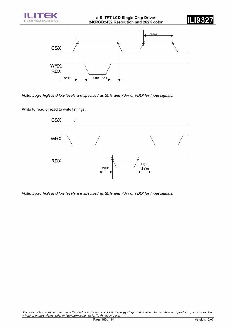
a-Si TFT LCD Single Chip Driver
240RGBx432 Resolution and 262K color ILI9327
The information contained herein is the exclusive property of ILI Technology Corp. and shall not be distributed, reproduced, or disclosed in whole or in part without prior written permission of ILI Technology Corp. Page 188 / 191 Version: 0.06
CSX
WRX,RDX
Min. 5nstcsf
tchw
Note: Logic high and low levels are specified as 30% and 70% of VDDI for Input signals.
Write to read or read to write timings:
twrhtrdh
tdhfm
CSX
WRX
RDX
`0'
Note: Logic high and low levels are specified as 30% and 70% of VDDI for Input signals.

a-Si TFT LCD Single Chip Driver
240RGBx432 Resolution and 262K color ILI9327
The information contained herein is the exclusive property of ILI Technology Corp. and shall not be distributed, reproduced, or disclosed in whole or in part without prior written permission of ILI Technology Corp. Page 189 / 191 Version: 0.06
15.3.2. DBI Type C (SPI) Interface Timing Characteristics
tccs
CSX
D/CX
SCL
DIN/SDA
DOUT
tcsh
tdcs tdch
tslw/tslr tshw/tshr
tscycw/tscycr
tacc toh
tsdhtsds
tchw tchw
Signal Symbol Parameter min max Unit Description
CSX
tcss CSX-SCL time (Write) 15 - ns tcsh CSX-SCL time (Write) 15 - ns tcss CSX-SCL time (Read) 60 - ns tcsh CSX-SCL time (Read) 60 - ns tchw CSX “H” pulse time 40 - ns
SCL
tscycw Serial clock cycle (Write) 60 - ns tshw SCL “H” pulse width (Write) 15 - ns tslw SCL “L” pulse width (Write) 15 - ns
tscycr Serial clock cycle (Read GRAM) 300 - ns tshr SCL “H” pulse width (Read GRAM) 110 - ns tslr SCL “L” pulse width (Read GRAM) 110 - ns
tscycr Serial clock cycle (Read ID) 150 - ns tshr SCL “H” pulse width (Read GRAM) 54 - ns tslr SCL “L” pulse width (Read GRAM) 54 - ns
D/CX tdcs D/CX setup time 7 - ns tdch D/CX hold time 7 - ns
SDA (Input)
(Output)
tacc Access time 10 50 ns For maximum CL=30pF For minimum CL=8pF toh Output disable time 15 50 ns
tsds Data setup time 7 - tsdh Data hold time 7 -
Note: Ta = -30 to 70 °C, VDDI=1.65V to 3.3V, VDD=2.5V to 3.0V, AGND=DGND=0V
tr≦15ns
70%
30%
70%
30%
tf≦15ns

a-Si TFT LCD Single Chip Driver
240RGBx432 Resolution and 262K color ILI9327
The information contained herein is the exclusive property of ILI Technology Corp. and shall not be distributed, reproduced, or disclosed in whole or in part without prior written permission of ILI Technology Corp. Page 190 / 191 Version: 0.06
15.3.3. DPI Interface Timing Characteristics
trgbftrgbr
tSYNCS
VIHVIL
tENS tENH
trgbrtrgbf
tPDHtPDStCYCD
PWDL PWDH
VIH
VIH
VIH VIH
VIH VIH
VIHVIL VIL
VIL
VIL
VIL
VIL
VSYNCHSYNC
ENABLE
Write Data
DOTCLK
D[17:0]
Signal Symbol Parameter min max Unit Description VSYNC / HSYNC
tSYNCS VSYNC/HSYNC setup time 15 - ns
18/16-bit bus RGB interface mode
tSYNCH VSYNC/HSYNC hold time 15 - ns
ENABLE tENS ENABLE setup time 15 - ns tENH ENABLE hold time 15 - ns
D[17:0] tPOS Data setup time 15 - ns tPDH Data hold time 15 - ns
DOTCLK
PWDH DOTCLK high-level period 15 - ns PWDL DOTCLK low-level period 15 - ns tCYCD DOTCLK cycle time 100 - ns
trgbr , trgbf DOTCLK,HSYNC,VSYNC rise/fall time - 15 ns VSYNC / HSYNC
tSYNCS VSYNC/HSYNC setup time 15 - ns
6-bit bus RGB interface mode
tSYNCH VSYNC/HSYNC hold time 15 - ns
ENABLE tENS ENABLE setup time 15 - ns tENH ENABLE hold time 15 - ns
D[17:0] tPOS Data setup time 15 - ns tPDH Data hold time 15 - ns
DOTCLK
PWDH DOTCLK high-level pulse period 15 - ns PWDL DOTCLK low-level pulse period 15 - ns tCYCD DOTCLK cycle time 100 - ns
trgbr , trgbf DOTCLK,HSYNC,VSYNC rise/fall time - 15 ns
Note: Ta = -30 to 70 °C, VDDI=1.65V to 3.3V, VDD=2.5V to 3.0V, AGND=DGND=0V
tr≦15ns
70%
30%
70%
30%
tf≦15ns

a-Si TFT LCD Single Chip Driver
240RGBx432 Resolution and 262K color ILI9327
The information contained herein is the exclusive property of ILI Technology Corp. and shall not be distributed, reproduced, or disclosed in whole or in part without prior written permission of ILI Technology Corp. Page 191 / 191 Version: 0.06
16. Revision History Version No. Date Page Description
0.00 2008/11/24 New Create 0.01 2009/03/03 13~18 Modify pad coordinates
2009/03/09 12, 18 Modify alignment mark coordinate y=-251 -217 13 Pad 166 modification: VREG VREG1OUT 2009/03/09 120~122 Add DSTB description 44~45 Add MDDI description and move DSTB description to page 120~122
0.02 2009/03/13 36 Add MDDI max transmit rate 130Mbps 0.03 2009/03/23 149, 181 Modify the gamma register RC8h and gamma adjustment.
7~9 Modify the pin description for the shared pins for sub-panel control 186, 187 Add the application circuit and power on/off sequence.
120 Modify the EPF definition. 0.04 2009/05/06 183 Remove the capacitors of VCOMH and VCOML. 0.05 2009/06/12 34
141 163 131
Modify the DPI (RGB) interface data bus arrangement. Modify the calculation formula of frame rate. Add GON/DTE/NW[5:0] description in register EAh. Update PWM output frequence
0.06 2009/06/15 117 Modify wait time after reset (31ms 100 msec)
With collaboration of https://www.displayfuture.com


