Download - ALICE Silicon Tracker Upgrade
ALICE SILICON TRACKER UPGRADEG. Contin – Universita` di Trieste & INFN Trieste
for the ALICE Collaboration
2
ALICE ITS Upgrade - G. Contin
• The present ALICE Inner Tracking System• ALICE Silicon Tracker Upgrade motivations• Detector requirements• Technology implementation
• Hybrid Pixel Detectors• Monolithic Pixel Detectors• Strip Detectors
• Conclusions
Summary
26/03/2012
3
The ALICE experiment
26/03/2012
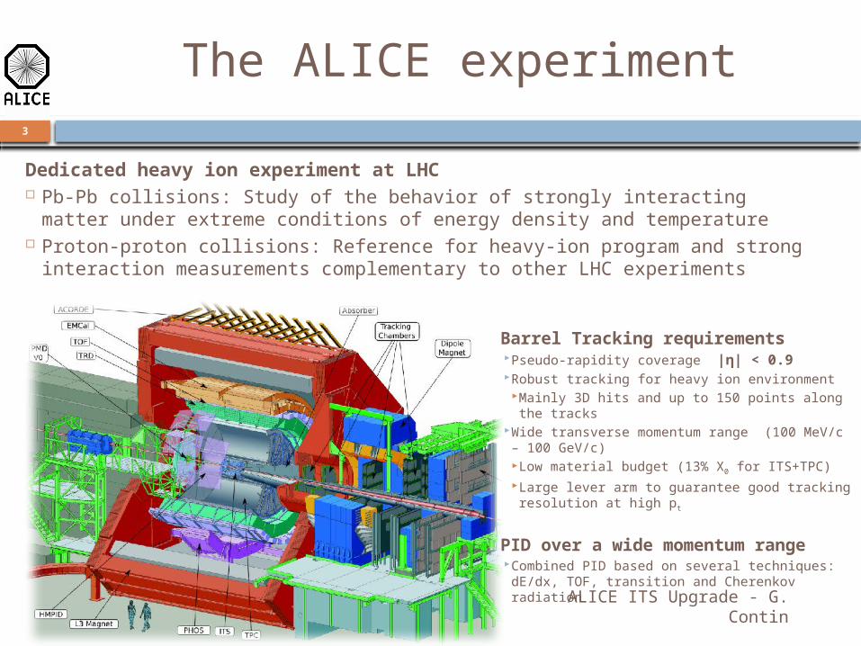
Dedicated heavy ion experiment at LHC Pb-Pb collisions: Study of the behavior of strongly interacting matter
under extreme conditions of energy density and temperature Proton-proton collisions: Reference for heavy-ion program and strong
interaction measurements complementary to other LHC experiments
Barrel Tracking requirements Pseudo-rapidity coverage |η| < 0.9 Robust tracking for heavy ion environment
Mainly 3D hits and up to 150 points along the tracks
Wide transverse momentum range (100 MeV/c – 100 GeV/c) Low material budget (13% X0 for ITS+TPC) Large lever arm to guarantee good tracking
resolution at high pt
PID over a wide momentum range Combined PID based on several techniques:
dE/dx, TOF, transition and Cherenkov radiationALICE ITS Upgrade - G. Contin
4
The present Inner Tracking System
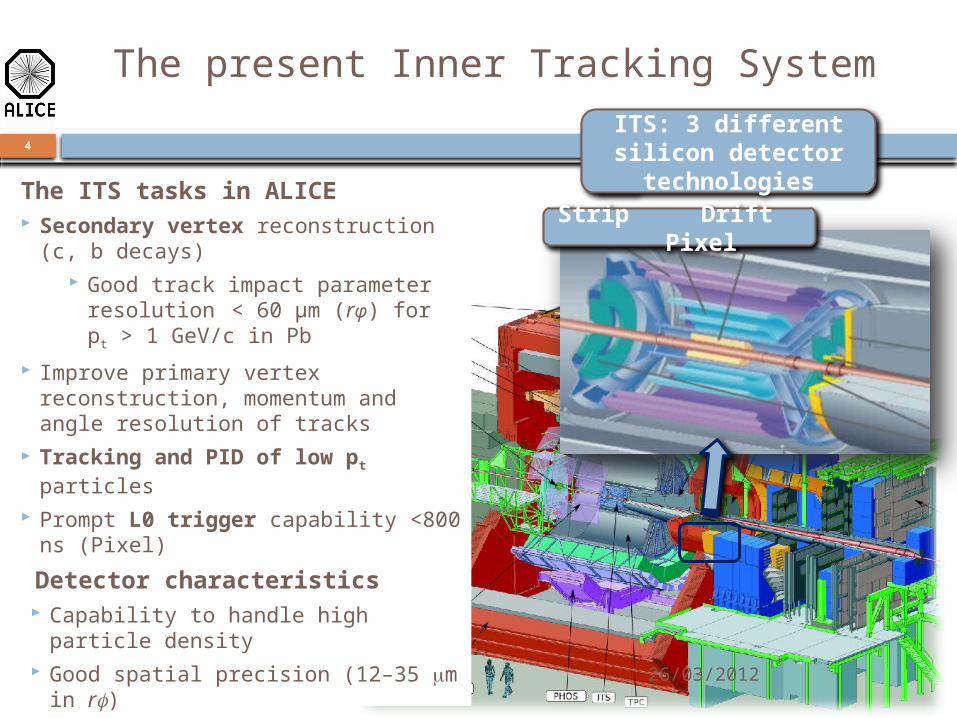
The ITS tasks in ALICE Secondary vertex reconstruction (c,
b decays) Good track impact parameter
resolution < 60 µm (rφ) for pt > 1 GeV/c in Pb
Improve primary vertex reconstruction, momentum and angle resolution of tracks
Tracking and PID of low pt particles
Prompt L0 trigger capability <800 ns (Pixel)
Detector characteristics Capability to handle high particle
density Good spatial precision (12–35 mm in
rf) High granularity (≈ few % occupancy) Small distance of innermost layer
from beam axis (mean radius ≈ 3.9 cm)
Limited material budget (7.2% X0)
Analogue information in 4 layers (Drift and Strip) for particle identification
ITS: 3 different silicon detector technologies
Strip Drift Pixel
26/03/2012
5
Physics Motivations for the Upgrade
26/03/2012ALICE ITS Upgrade - G.
Contin
Quark mass dependence of in-medium energy loss Thermalization of heavy quarks in the medium
Improve the charmed baryonic sector studies Access the exclusive measurement of beauty hadrons
Reconstruct displaced decay vertices Track charged particles with high resolution at all momenta Identify charged particles down to low transverse
momentum Implement a topological trigger functionality
Motivations
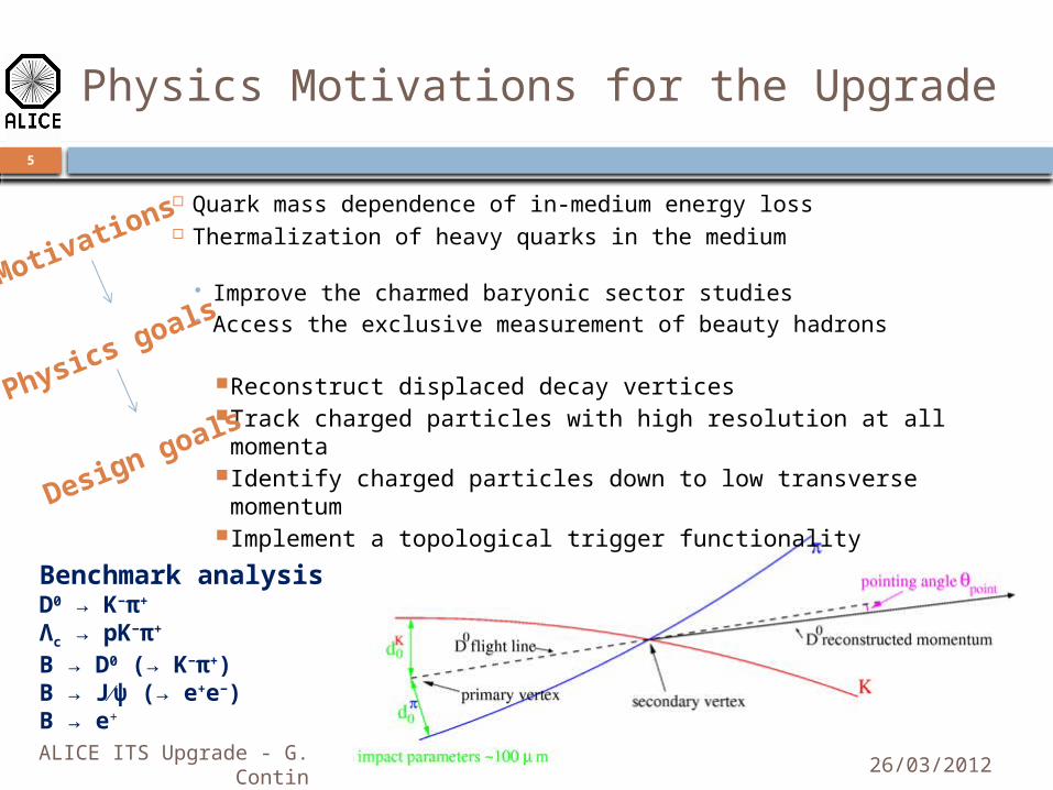
Benchmark analysisD0 → K−π+
Λc → pK−π+
B → D0 (→ K−π+)B → J∕ψ (→ e+e−)B → e+
Physics goals
Design goals

6
From Design Goals to Detector Requirements
Impact parameter resolution improvement by a factor 3 Distance from interaction vertex Material budget Spatial precision
Standalone tracking efficiency and transverse momentum resolution Granularity Radial extension Layer grouping
Experimental environment: 685 krad, 80 part/cm2
Radiation hardness, granularity Interaction rates: 50 kHz in Pb-Pb, 2 MHz in pp
Fast readout Particle identification capability
Energy loss measurement resolution and range Expected detector lifetime
Detector accessibility and modularity
Geometry and technology for innermost layers
dE/dx, ToT techniques
Position of the outermost layersStrip cell size reduction for intermediate radii
Pixel cell size reduction for inner layers
Layout, supports, services
Technology for innermost layers
Readout architecture
26/03/2012ALICE ITS Upgrade - G. Contin
7
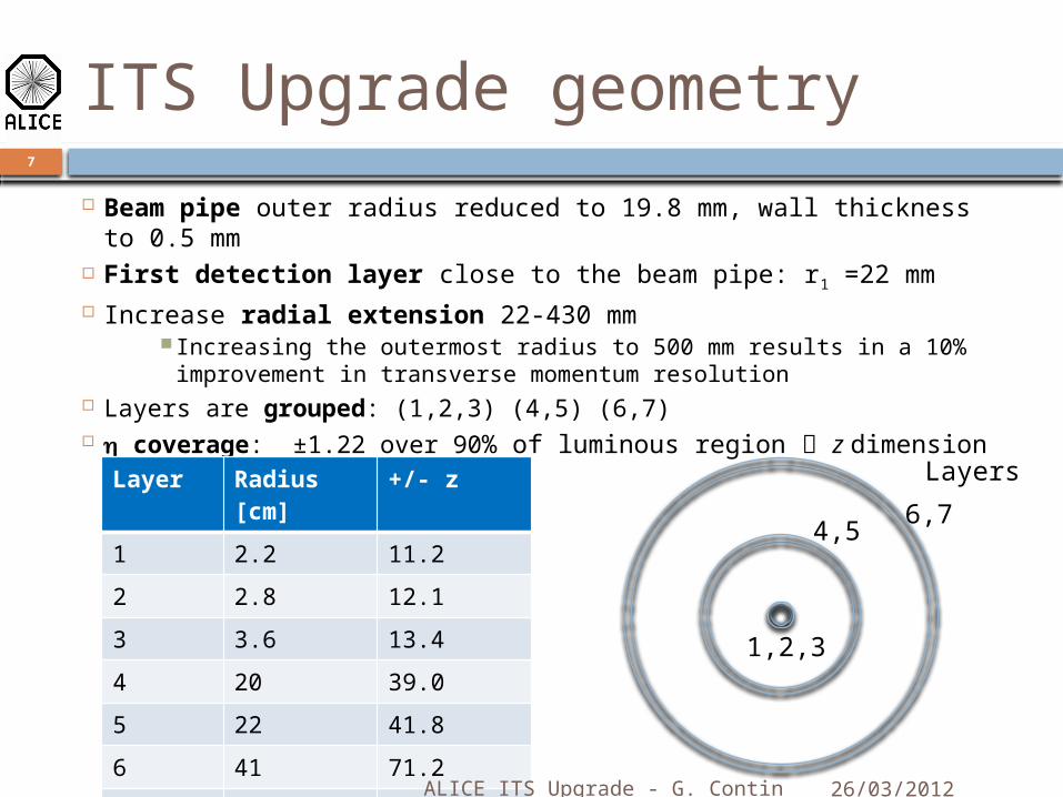
ITS Upgrade geometry
Beam pipe outer radius reduced to 19.8 mm, wall thickness to 0.5 mm
First detection layer close to the beam pipe: r1 =22 mm Increase radial extension 22-430 mm
Increasing the outermost radius to 500 mm results in a 10% improvement in transverse momentum resolution
Layers are grouped: (1,2,3) (4,5) (6,7) h coverage: ±1.22 over 90% of luminous region z dimension
Layer Radius [cm]
+/- z
1 2.2 11.2
2 2.8 12.1
3 3.6 13.4
4 20 39.0
5 22 41.8
6 41 71.2
7 43 74.3
6,74,5
1,2,3
Layers
26/03/2012ALICE ITS Upgrade - G. Contin

8
How Detector Requirements drive Technology Choices
rf & z spatial precision: 4 mm Pixel size (rf , z): 20-30 , 20-50
mm Material budget per layer: 0.3-
0.5% X0
0.1% X0 under study for Layer 1
Radiation env: 685 krad/ 1013 neq per year
Granularity: 80 cm-2 particle density
rf spatial precision: < 20 mm Larger pixel size Strip pitch 95 mm, stereo angle 35
mrad Material budget per layer: 0.5-
0.8% X0
Radiation env: 10 krad/ 3*1011 neq per year
Granularity: 1 cm-2 particle density Low cost per m2
26/03/2012ALICE ITS Upgrade - G. Contin
Targets for Inner Layers (1, 2, 3)
Targets for Outer Layers (4, 5, 6, 7)
Monolithic pixelHybrid pixel
Monolithic pixelMicro-strip

9
2 layout options
26/03/2012ALICE ITS Upgrade - G.
Contin
A. 7 layers of monolithic pixel detectors Better standalone tracking efficiency and transverse momentum
resolution Worse PID or no PID
B. 3 innermost layers of hybrid pixel + 4 layers of micro strip detectors
Worse standalone tracking efficiency and transverse momentum resolution
Optimal PID
7 layers of pixels
Option A
3 layers of pixels
4 layers of strips
Option B
Pixels: O( 20 µm x 20 µm )Pixels: O( 20x20µm2 – 50 x 50µm2)Strips: 95 µm x 2 cm, double sided
685 krad/ 1013 neq per year

ALICE ITS Upgrade - G. Contin
10
Monolithic Pixel technology
26/03/2012
Features: Made significant progress, soon to be installed in STAR All-in-one, detector-connection-readout Sensing layer (moderate resistivity ~1 kWcm epitaxial
layer) included in the CMOS chip Charge collection mostly by diffusion (MAPS), but some
development based on charge collection by drift Small pixel size: 20 mm x 20 mm target size Small material budget: 0.3% X0 per layer
To be evaluated Radiation tolerance
Options under study:• MIMOSA• INMAPS• LePIX

ALICE ITS Upgrade - G. Contin
11
Monolithic: MIMOSA (IPHC)
26/03/2012
CMOS sensors with rolling-shutter readout architecture
MIMOSA series for STAR Continuous charge collection (mostly by diffusion) inside the
pixel Charge collection time ~200 ns
Pixel matrix read periodically row by row: column parallel readout with end of column discriminators Integration time readout period ~100 ms Low power consumption (150-250 mW/cm2): only one row
is powered at time Pixel size 20 mm Total material budget x ~ 0.3% X0
0.35 mm technology node ULTIMATE sensor for STAR HFT
ALICE ITS Upgrade - G. Contin
12
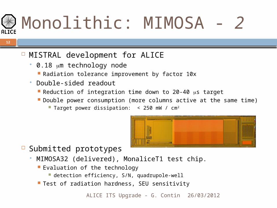
Monolithic: MIMOSA - 2
26/03/2012
MISTRAL development for ALICE 0.18 mm technology node
Radiation tolerance improvement by factor 10x Double-sided readout
Reduction of integration time down to 20-40 ms target Double power consumption (more columns active at the same time)
Target power dissipation: < 250 mW / cm2
Submitted prototypes MIMOSA32 (delivered), MonaliceT1 test chip.
Evaluation of the technology detection efficiency, S/N, quadrupole-well
Test of radiation hardness, SEU sensitivity
ALICE ITS Upgrade - G. Contin
13
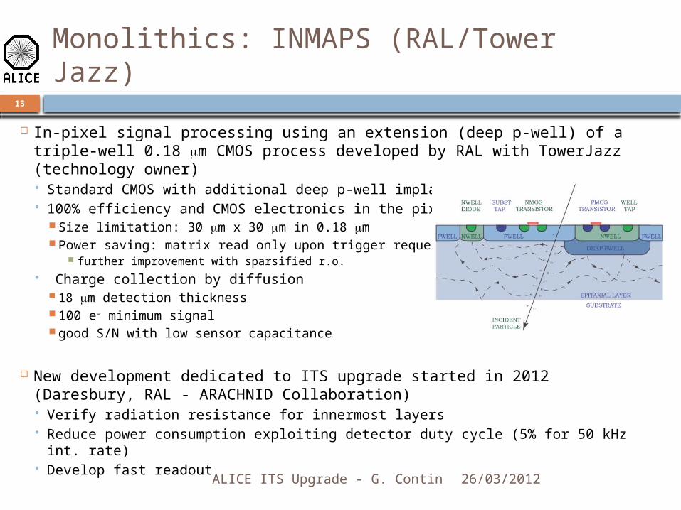
Monolithics: INMAPS (RAL/Tower Jazz)
26/03/2012
In-pixel signal processing using an extension (deep p-well) of a triple-well 0.18 mm CMOS process developed by RAL with TowerJazz (technology owner) Standard CMOS with additional deep p-well implant 100% efficiency and CMOS electronics in the pixel
Size limitation: 30 mm x 30 mm in 0.18 mm Power saving: matrix read only upon trigger request
further improvement with sparsified r.o. Charge collection by diffusion
18 mm detection thickness 100 e- minimum signal good S/N with low sensor capacitance
New development dedicated to ITS upgrade started in 2012 (Daresbury, RAL - ARACHNID Collaboration)
Verify radiation resistance for innermost layers Reduce power consumption exploiting detector duty cycle (5% for 50 kHz int.
rate) Develop fast readout

14
Monolithics: LePIX
26/03/2012ALICE ITS Upgrade - G. Contin
Monolithic pixel detectors integrating readout and detecting elements with: 90 nm CMOS technology Moderate resistivity wafers
Low power consumption (target < 30mW / cm2) Large depletion region (tens of mm) Fast processing: full matrix readout at 40MHz Moderate bias voltage (< 100 V)
Tests on standard resistivity prototypes Large breakdown voltage (>30 V) 50 mm depletion is achievable Small collection capacitance (<1 fF) high S/N, small power
consumption Qualification for radiation hardness
Charge collected by drift Reduce irradiation bulk damage Control charge sharing Improve charge collection speed
Large Signal-to-Noise ratio PID with large depletion region
ALICE ITS Upgrade - G. Contin
15
Hybrid Pixels and Ongoing R&D
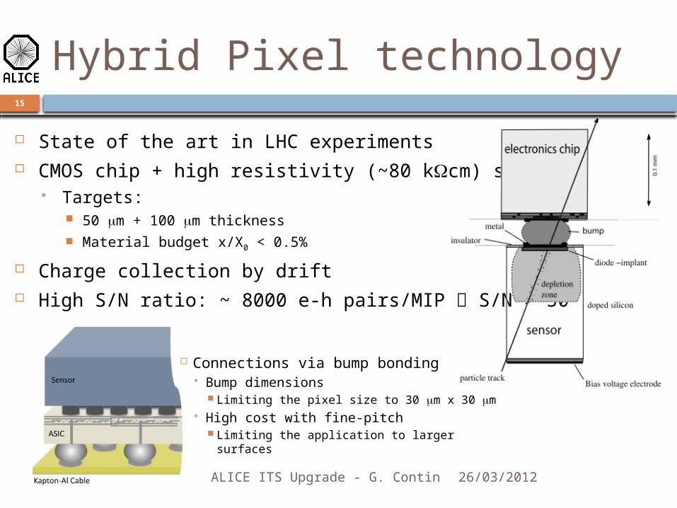
Hybrid Pixel technology
State of the art in LHC experiments CMOS chip + high resistivity (~80 kWcm) sensor
Targets: 50 mm + 100 mm thickness Material budget x/X0 < 0.5%
Charge collection by drift High S/N ratio: ~ 8000 e-h pairs/MIP S/N > 50
Connections via bump bonding Bump dimensions
Limiting the pixel size to 30 mm x 30 mm High cost with fine-pitch
Limiting the application to larger surfaces
26/03/2012
ALICE ITS Upgrade - G. Contin
16
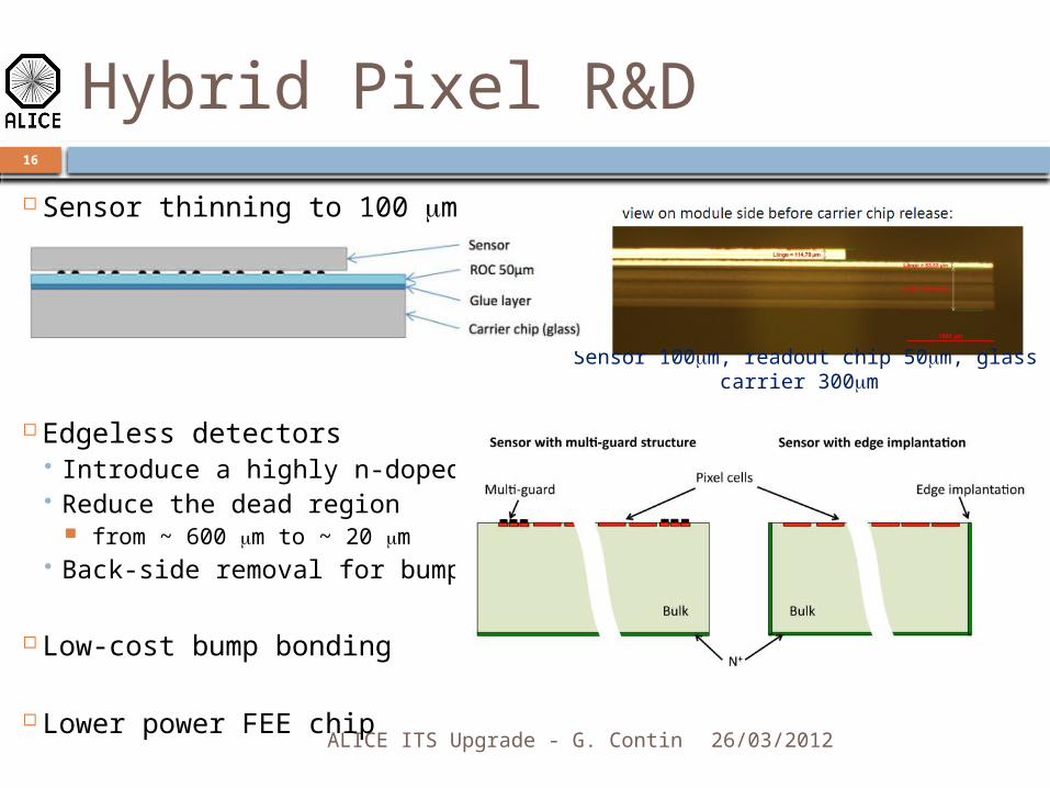
Hybrid Pixel R&D
26/03/2012
Sensor thinning to 100 mm
Edgeless detectors Introduce a highly n-doped trench Reduce the dead region
from ~ 600 mm to ~ 20 mm Back-side removal for bumping
Low-cost bump bonding
Lower power FEE chip
Sensor 100mm, readout chip 50mm, glass carrier 300mm
17
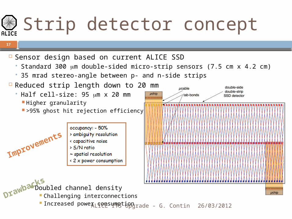
Strip detector concept
26/03/2012ALICE ITS Upgrade - G. Contin
Sensor design based on current ALICE SSD Standard 300 mm double-sided micro-strip sensors (7.5 cm x 4.2 cm) 35 mrad stereo-angle between p- and n-side strips
Reduced strip length down to 20 mm Half cell-size: 95 mm x 20 mm
Higher granularity >95% ghost hit rejection efficiency
Doubled channel density Challenging interconnections Increased power consumption
Improvements
Drawbacks
18
Strip detector development
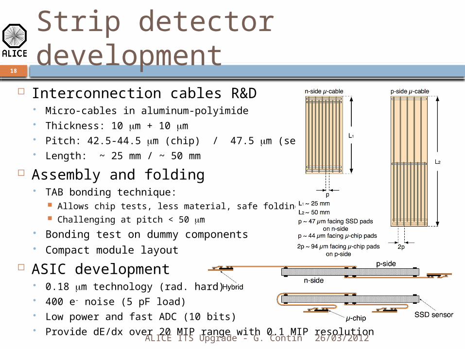
Interconnection cables R&D Micro-cables in aluminum-polyimide Thickness: 10 mm + 10 mm Pitch: 42.5-44.5 mm (chip) / 47.5 mm (sensor) Length: ~ 25 mm / ~ 50 mm
Assembly and folding TAB bonding technique:
Allows chip tests, less material, safe folding Challenging at pitch < 50 mm
Bonding test on dummy components Compact module layout
ASIC development 0.18 mm technology (rad. hard) 400 e- noise (5 pF load) Low power and fast ADC (10 bits) Provide dE/dx over 20 MIP range with 0.1 MIP resolution26/03/2012ALICE ITS Upgrade - G. Contin
19
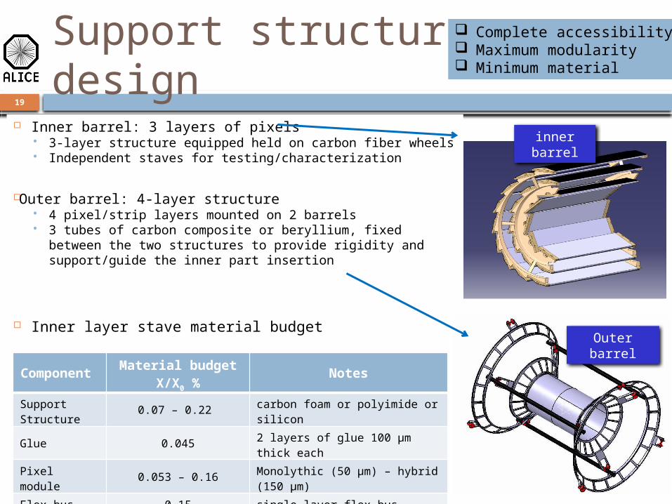
Support structure design
26/03/2012
Inner barrel: 3 layers of pixels 3-layer structure equipped held on carbon fiber
wheels Independent staves for testing/characterization
Outer barrel: 4-layer structure 4 pixel/strip layers mounted on 2 barrels 3 tubes of carbon composite or beryllium, fixed
between the two structures to provide rigidity and support/guide the inner part insertion
Inner layer stave material budget Outer barrel
inner barrel
ALICE ITS Upgrade - G. Contin
Complete accessibility Maximum modularity Minimum material
Component Material budget X/X0 % Notes
Support Structure 0.07 – 0.22 carbon foam or polyimide or silicon
Glue 0.045 2 layers of glue 100 µm thick each
Pixel module 0.053 – 0.16 Monolythic (50 µm) – hybrid (150 µm)
Flex bus 0.15 single layer flex bus
Total 0.32 – 0.58
ALICE ITS Upgrade - G. Contin
20
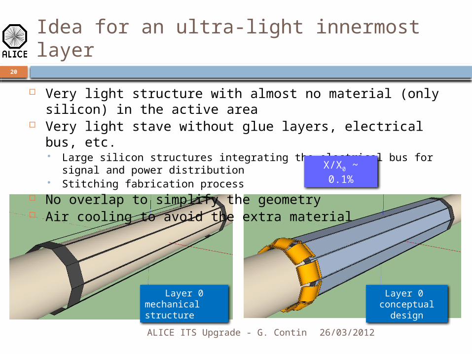
Idea for an ultra-light innermost layer
26/03/2012
Very light structure with almost no material (only silicon) in the active area
Very light stave without glue layers, electrical bus, etc. Large silicon structures integrating the electrical bus for signal and
power distribution Stitching fabrication process
No overlap to simplify the geometry Air cooling to avoid the extra material
Layer 0mechanical structure
Layer 0 conceptual design
X/X0 ~ 0.1%
ALICE ITS Upgrade - G. Contin
21
Conclusions
26/03/2012
The ALICE Silicon Tracker Upgrade is required to study: Quark mass dependence of in-medium energy loss Thermalization of heavy quarks in the medium
New Tracker composed of 7 silicon layers characterized by: Impact parameter resolution improved by factor 3x First detecting layer @20 mm from the beam line Material budget x/X0 ~ 0.3-0.5 % in the first layers High spatial precision (~ 4 mm in the first layers) Very high standalone tracking efficiency down to low pt (> 95% for pt > 200 MeV/c) PID capability Fast access for maintenance
Detector technologies considered for the Upgrade Monolithic Pixel Detectors Hybrid Pixel Detectors Micro-Strip Detectors
Low material budget supports allowing access and repair To be built and installed by 2019!!!

22
ALICE ITS Upgrade - G. Contin
Backup slides
26/03/2012
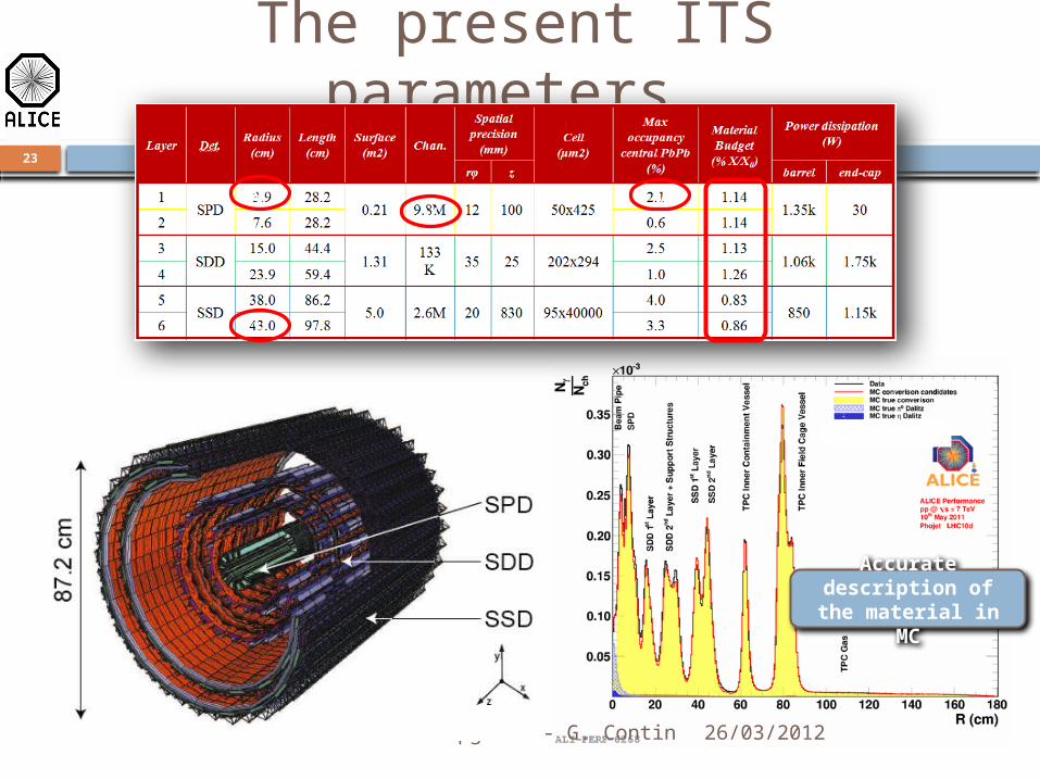
The present ITS parameters
26/03/2012ALICE ITS Upgrade - G. Contin
23
v
v
vv
Accurate description of the
material in MC

24
Layout 1: “All New” – Pixels (7 pixel layers)• Resolutions: srf = 4 mm, sz = 4 mm for all layers • Material budget: X/X0 = 0.3% for all layers Layout 2: Pixel/Strips (3 layers of pixels + 4 layers of strips)• Resolutions: srf = 12 mm, sz = 12 mm for pixels srf = 20 mm, sz = 830 mm for strips • Material budget: X/X0 = 0.5% for pixels X/X0 = 0.83% for strips
radial positions (cm): 2.2, 2.8, 3.6, 20, 22, 41, 43
Same for both layouts
Simulations for two upgrade layouts HYBRID PIXELS (state-of-the-art) and comparison with MAPS
Improvement of impact parameter resolution & tracking efficiency
ALICE ITS Upgrade - G. Contin
25
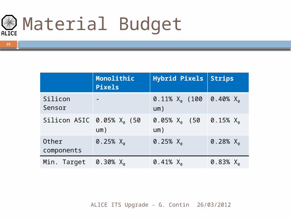
Material Budget
26/03/2012
Monolithic Pixels
Hybrid Pixels Strips
Silicon Sensor - 0.11% X0 (100 um)
0.40% X0
Silicon ASIC 0.05% X0 (50 um)
0.05% X0 (50 um)
0.15% X0
Other components
0.25% X0 0.25% X0 0.28% X0
Min. Target 0.30% X0 0.41% X0 0.83% X0
26
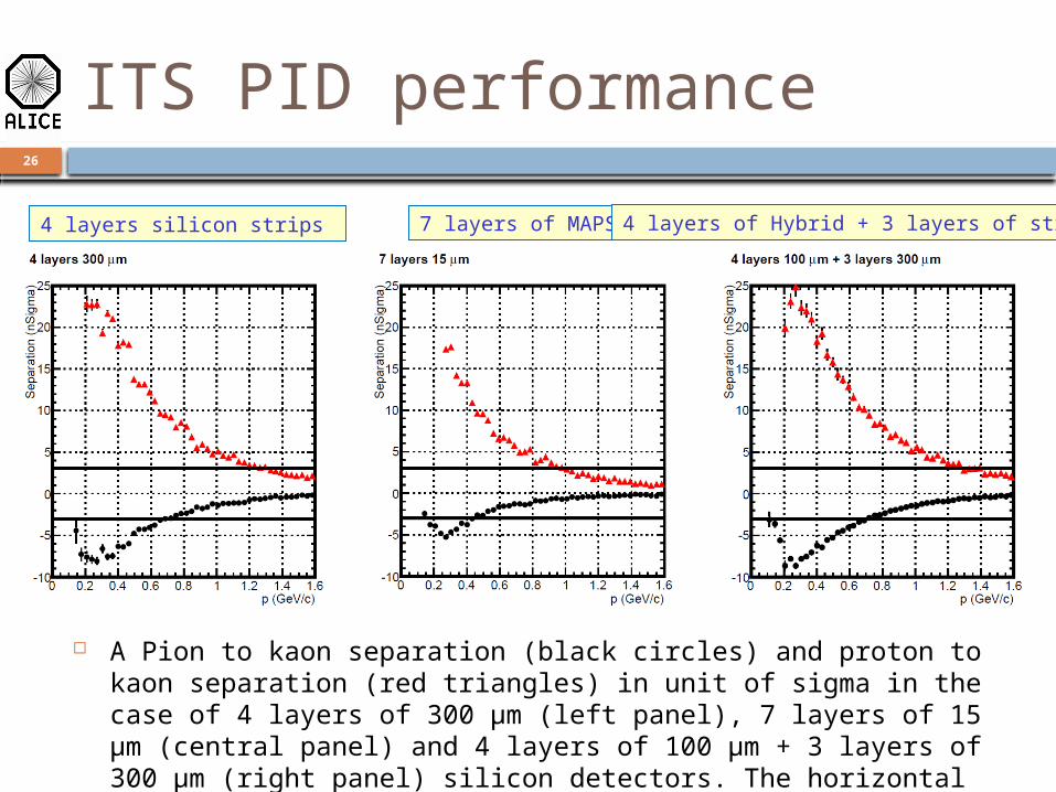
4 layers silicon strips 7 layers of MAPS 4 layers of Hybrid + 3 layers of strips
ITS PID performance
A Pion to kaon separation (black circles) and proton to kaon separation (red triangles) in unit of sigma in the case of 4 layers of 300 μm (left panel), 7 layers of 15 μm (central panel) and 4 layers of 100 μm + 3 layers of 300 μm (right panel) silicon detectors. The horizontal lines correspond to a 3 sigma separation.