Download - ANALYSIS AND DESIGN OF BROADBAND MICROWAVE …
ANALYSIS AND DESIGN OF BROADBAND MICROWAVE DISTRIBUTED
AMPLIFIERS
REYHAN YURT
JUNE 2017

ANALYSIS AND DESIGN OF BROADBAND MICROWAVE DISTRIBUTED
AMPLIFIERS
A THESIS SUBMITTED TO
THE GRADUATE SCHOOL OF NATURAL AND APPLIED
SCIENCES OF
ÇANKAYA UNIVERSITY
BY
REYHAN YURT
IN PARTIAL FULFILLMENT OF THE REQUIREMENTS FOR THE
DEGREE OF
MASTER OF SCIENCE
IN
THE DEPARTMENT OF
ELECTRONIC AND COMMUNICATION ENGINEERING
JUNE 2017


iv
ABSTRACT
Analysis and design broadband microwave distributed amplifiers
YURT, Reyhan
M.Sc., Department of Electronic and Communication Engineering
Supervisor: Prof. Dr. Halil Tanyer EYYUBOĞLU
June 2017, 78 pages
In this thesis, microwave amplifier design techniques are analyzed and especially
distributed technique is applied for broadband amplifier in L-S band according to the
IEEE radar-frequency band. Conventional distributed amplifier (CDA) design
topology is implied at 1-3 GHz frequency range. Available gain is obtained 14+2.5
dB with flatness. Optimum number of stages of amplifier is investigated and the
result is evaluated as restriction of this topology so amplifier is designed with one
stage. To increase gain performance cascaded single stage distributed amplifier
(CSSDA) topology is analyzed and designed as 2-CSSDA at 1-3 GHz. In this design,
almost 26 dB is obtained as peak value of available gain near 2.7 GHz and available
gain is observed as 23.9+2 dB with simulations. CSSDA designed topology can be
integrated with breakthrough circuit and approach so that more qualified distributed
amplifier (DA) may be improved.
Keywords: Broadband Microwave Amplifier, Distributed Amplifier, Conventional
Distributed Amplifier, CSSDA
v
ÖZ
Mikrodalga Geniş Bantlı Dağıtılmış Yükselteçlerin Analizi ve Tasarımı
YURT, Reyhan
Yüksek Lisans, Elektronik ve Haberleşme Mühendisliği Anabilim Dalı
Tez Yöneticisi: Prof. Dr. Halil Tanyer EYYUBOĞLU
Haziran 2017, 78 sayfa
Bu tezde, mikrodalga yükselteç teknikleri incelenmiş ve IEEE radar frekans bandına
göre özellikle dağıtılmış yükselteç tekniği L-S bantta geniş bantlı mikrodalga
yükselteç için uygulanmıştır. Geleneksel dağıtılmış yükselteç tasarım topolojisi 1-3
GHz frekans aralığında uygulanmıştır. Mevcut kazanç 14+2.5 dB düzgün olarak elde
edilmiştir. Yükseltecin en uygun aşama sayısı araştırılmış ve sonuç bu topolojinin bir
sınırlaması olarak değerlendirilmiştir ve bu yuzden yükselteç bir aşama ile
tasarlanmıştır. Kazanç performansını arttırmak için, seri bağlı tek aşamalı dağıtılmış
yükselteç topolojisi incelenmiştir ve 1-3 GHz ‘de 2-SBTADY olarak tasarlanmıştır.
Bu tasarımda, simulasyonlar ile yaklaşık 26 dB mecvut kazancın en yüksek değeri
olarak 2.7 GHz civarında elde edilmiştir ve mevcut kazanç 23.9+2 dB olarak
gözlemlenmiştir. Tasarlanan SBTADY topolojisi, büyük yenilik içeren devre ve
yaklaşımla entegre edilebilir böylece daha nitelikli DY geliştirilebilir.
Anahtar Kelimeler: Geniş Bantlı Mikrodalga Yükselteç, Dağıtılmış Yükselteç,
Geleneksel Dağıtılmış Yükselteç, Seri Bağlı Tek Aşamalı Dağıtılmış Yükselteç

vi
to my parents and nephew Ömer Asaf,

vii
ACKNOWLEDGEMENTS
I would like to thank my supervisor Prof. Dr. Halil Tanyer EYYUBOĞLU for his
guidance and suggestions throughout this thesis study.
I would like to express special thanks to Doç. Dr. Mehmet YÜCEER. I am really
thankful to him because I started to study at this field with just one course and he was
so helpful for my first studies in microwave amplifier world as instructor of this
course. Moreover, he helped me to develop myself and gain a point of view in
designing microwave amplifier.
I would like to thank the jury members for their valuable comments on the thesis.
I am really thankful to Dean of Engineering Faculty of Yalova University Prof. Dr.
Mustafa ÖZTAŞ for their valuable support.
I am grateful to my family for their support and their unfailing encouragement during
this study.

viii
TABLE OF CONTENTS
STATEMENT OF NON PLAGIARISM................................................................. iii
ABSTRACT.............................................................................................................. iv
ÖZ………………………………………………………………………………….. v
ACKNOWLEDGEMENTS……………………………………………………….. vii
TABLE OF CONTENTS………………………………………………………….. viii
LIST OF FIGURES……………………………………………………………….. x
LIST OF TABLES…………………………………………………………………. xiii
LIST OF ABBREVIATIONS……………………………………………………... xiv
CHAPTERS:
1. INTRODUCTION........................................................................................ 1
1.1. RF and Microwave Amplifiers …..................................................... 1
1.2. Two Ports Network……………........................................................ 2
1.3. Impedance Matching and Main Parameters....................................... 5
1.4. Organization of Thesis………………………..……………………. 11
2. BROADBAND AMPLIFICATION…........................................................ 12
2.1. Overview of Broadband Amplifiers ………………………............. 12
2.2. Methods of Broadband Amplifiers………………………………… 12
2.3. Distributed Amplification…….…………......................................... 16
3. ANALYSIS OF DISTRIBUTED AMPLIFIER.......................................... 19
3.1. Principles of Distributed Amplifier………………………………… 19
3.2. Analytical Analysis of Distributed Amplifier................................... 21
3.3. About Transistors Used in Case Study……...................................... 24
3.4. Stability Analysis……………………………………….…….......... 25
3.5. Bias Circuit of Used Transistor……………………………………. 27
3.6. Input and Output Matching Circuits………………………………. 28
ix
4. DESIGN OF THE DISTRIBUTED AMPLIFIER…………………………… 32
4.1. Design and Simulation Results of Conventional Distributed Single
Stage Distributed Amplifier…………………………………………...
32
4.2 Proposed Design of Single Stage Distributed Amplifier……………… 42
4.3 2- Cascaded Single Stage Distributed Amplifier……………………… 49
5. CONCLUSION……...................................................................................... 55
REFERENCES............................................................................................................ 58
APPENDICES………………………………………………………………………. 61
A. DIE MODEL OF ATF-54143……………………………………………….. 61
B. TOUCHSTONE FILE OF ATF-54143 FOR Vds= 3V, Ids= 60mA………… 62
x
LIST OF FIGURES
FIGURES
Figure 1 Basic block diagram of microwave transistor amplifier [3]…… 2
Figure 2 Two port network……………………………………………… 3
Figure 3 Incident and emerging waves...................................................... 4
Figure 4 Input matching on Smith Chart………………………………... 6
Figure 5 Output matching on Smith Chart………………………………. 7
Figure 6 Input and output matching networks (left-input, right-output) ... 7
Figure 7 WithImpedanceMatching and WithoutImpedanceMatching
circuit schematics……………………………………………… 8
Figure 8 Comparison between matched and unmatched network………. 9
Figure 9 Lossy matched amplifier topology (given in [15])…………….. 13
Figure 10 Balanced amplifier topology (given in [9])……………………. 14
Figure 11 Feedback amplifier topology (given in [15]) …………………. 16
Figure 12 Basic diagram of N-stage distributed amplifier (given in [9])… 18
Figure 13 Simplified schematic of 2 – DA with lumped elements [21]….. 19
Figure 14 Basic concept of conventional distributed amplifier…...…...... 20
Figure 15 The equivalent circuit of a single unit cell of the gate line [9]… 21
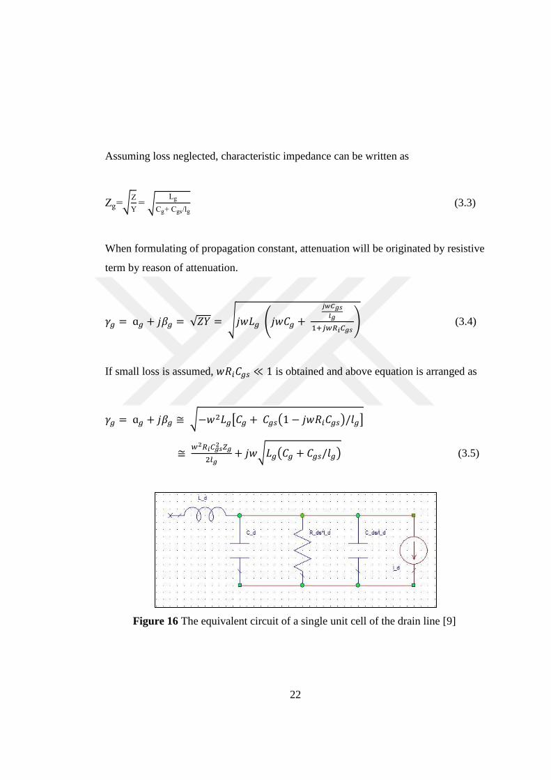
Figure 16 The equivalent circuit of a single unit cell of the drain line [9].. 22
Figure 17 Stability analysis of ATF-54143 at operating frequency range
for Vds=3V and Ids=60 mA s…………………………………. 25
Figure 18 Stability circuit schematic…………………............................... 26
Figure 19 Stability analysis after the connecting stability circuit............... 26

xi
Figure 20 Bias circuit schematic…………………………………………. 27
Figure 21 Input matching on Smith Chart ………………………………. 30
Figure 22 Output matching on Smith Chart………..................................... 31
Figure 23 Input and output impedance matching circuits (left -input
matching, right –output matching)…………………………….. 31
Figure 24 Basic schematics of T type and L type artificial transmission
lines [25]……………………………………………………….. 34
Figure 25 Conventional single stage distributed amplifier schematic……. 35
Figure 26 Available gain single stage distributed amplifier……………… 36
Figure 27 S parameters in logarithmic magnitude (in dB) of conventional
SSDA…………………………………………………………. 37
Figure 28 Input matching on Smith Chart……………………………….. 38
Figure 29 Output matching on Smith Chart.…………………………….. 39
Figure 30 Input and output matching circuits of conventional SSDA….. 39
Figure 31 Schematic of impedance matched conventional SSDA……… 40
Figure 32 Available gains of SSDA and impedance matched SSDA….. 41
Figure 33 Stability control of conventional single stage distributed
amplifier………………………………………………………. 42
Figure 34 Optimized single stage distributed amplifier…………………. 45
Figure 35 Gain performance of optimized SSDA and conventional SSDA
amplifier designs ……………………………………………… 46
Figure 36 Stability Analysis of optimized single stage distributed
amplifier……………………………………………………….. 47
Figure 37 S parameters (in dB) of optimized single stage distributed
amplifier……………………………………………………….. 48
Figure 38 Designed 2-CSSDA schematic………………………………… 49
Figure 39 Stability analysis of 2-CSSDA ………………………………... 50
Figure 40 Gain performance of 2-Cascaded SSDA ……………………… 51
Figure 41 S Parameters of 2-Cascaded SSDA ………………………….... 52

xii
Figure 42 Gain analyses of 2-CSSDA and conventional SSDAs ………... 53
Figure 43 Noise figure comparison of conventional DAs and CSSDA ….. 54

xiii
LIST OF TABLES
TABLES
Table 1
Input and output impedances of unconditionally stable
transistor at 1.6-2.4 GHz………………………………………..
6
Table 2
Input and output impedances of biased circuit for impedance
matching circuits………………………………………………..
31
Figure 3 Input and output impedances of biased circuit at 1-3 GHz……. 39
xiv
LIST OF ABBREVIATIONS
RF Radio Frequency
DA Distributed Amplifier
TWT Traveling Wave Tube
S-
Parameters Scattering Parameters
MTA Microwave Transistor Amplifier
CAD Computer-Aided Design
BJT Bipolar Junction Transistor
FET Field Effect Transistor
PHEMT Pseudormphic High Electron Mobility Transistor
CDA Conventional Distributed Amplifier
CSSDA Cascaded Single Stage Distributed Amplifier
SSDA Single Stage Distributed Amplifier

1
CHAPTER 1
INTRODUCTION
1.1 RF and Microwave Amplifiers
In radio frequency and microwave communication systems, amplifier is one of the
most significant components. Signal amplification is required to transfer message
signal with determined power gain or and noise figure. Moreover, amplifier can be
designed for transmitter and receiver antenna to achieve transmission with
undistorted signal, high gain and low noise figure thanks to low design approaches.
In the past, amplification function was carried out with Klystron, traveling-wave
tubes (TWT) and magnetrons [1]. However, today developing semi-conductor
technologies has provided opportunities to use transistors. Therefore, solid state
amplifiers [2] can be designed for systems which need approximately at most 100
watts.
According to the system which includes amplifier in, design criteria varies. High-
gain, bandwidth and low noise are the most important amplifier requirements for
microwave engineering areas such as radars, satellite communication and optical
communication also, point to point, point to multipoint and multipoint to multipoint
radio links. In addition, transistor amplifiers are commonly preferred in today
wireless communication technologies because of these basic requirements.
MTA (Microwave Transistor Amplifier) fundamentally consists of input and output
matching circuits, bias circuit and stability, gain-flatness and low noise networks can
be made available if these features are placed in system requirements. 50Ω, 75Ω or

2
100Ω system impedances are matched to active device input and output port
according to its scattering parameters which is determined based on frequency.
In this study, 50Ω system impedance is matched with transistor according to its gate
to source and drain to source capacitances by drawing artificial inductive
transmission lines for all configurations of distributed amplifier. After that, by
helping AWR Microwave Office CAD tool simulations are carried out. Also,
simulation results are used to analyze designed amplifier circuit by using AWR
Microwave Office CAD tool as design environment. Moreover, schematics are
drawn to explain topologies in thesis in AWR Microwave Office Project-Circuit
Schematics part such as in Fig.1 represents basic transistor amplifier diagram.
Figure 1 Basic block diagram of microwave transistor amplifier [3]
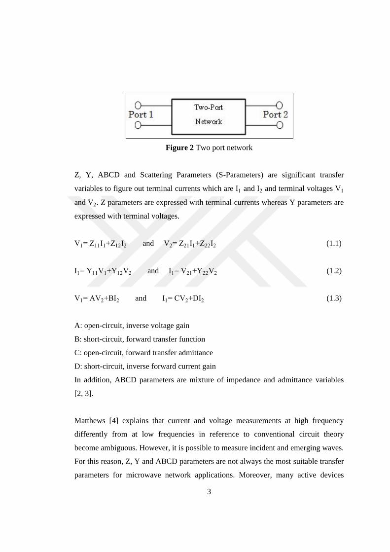
1.2 Two Port Network
System ports which have one or more ports are accepted as networks. They
correspond to a pair of electrical terminals describe electrical behavior of active and
passive devices. As in Fig.2 these ports are named “Port 1” and “Port 2” or input and
output ports. When designing amplifier mostly input and output ports are used.
3
Figure 2 Two port network
Z, Y, ABCD and Scattering Parameters (S-Parameters) are significant transfer
variables to figure out terminal currents which are I1 and I2 and terminal voltages V1
and V2. Z parameters are expressed with terminal currents whereas Y parameters are
expressed with terminal voltages.
V1= Z11I1+Z12I2 and V2= Z21I1+Z22I2 (1.1)
I1= Y11V1+Y12V2 and I1= V21+Y22V2 (1.2)
V1= AV2+BI2 and I1= CV2+DI2 (1.3)
A: open-circuit, inverse voltage gain
B: short-circuit, forward transfer function
C: open-circuit, forward transfer admittance
D: short-circuit, inverse forward current gain
In addition, ABCD parameters are mixture of impedance and admittance variables
[2, 3].
Matthews [4] explains that current and voltage measurements at high frequency
differently from at low frequencies in reference to conventional circuit theory
become ambiguous. However, it is possible to measure incident and emerging waves.
For this reason, Z, Y and ABCD parameters are not always the most suitable transfer
parameters for microwave network applications. Moreover, many active devices

4
become unstable when they are terminated with open and short circuits so S
parameters provide an advantage for active network.
Wave propagation is considered in short-wave length circuit at high frequencies.
Incident and emerging waves affect many dimensions such as power, phase,
reflection coefficients from load to source [4, 5, 6]. Therefore, physical terminal
behaviors such as reflection coefficient, return loss, gain and the numbers of incident
and emerging waves are expressed by means of complex S- parameters based upon
frequency. In Fig.3, there is a diagram which represents basically incident and
emerging wave’s relation with network.
Figure 3 Incident and emerging waves
an:Incident wave
bn:Emerging wave
Z0:Characteristic impedance
Vn+:Potential toward network
Vn- :Potential outward network
The following equations define the wave numbers and S-parameters for two port
network [2, 3, 4, 6] :
𝑎𝑛 = 𝑉𝑛
+
√𝑍0 and bn=
Vn-
√Z0 (1.4)
b1 = S11a1+S12a2 and b2= S21a1+S22a2 (1.5)

5
S11 parameter of an amplifier express input reflection coefficient [3] and its
logarithmic magnitude defines input return loss. In other words, input return loss
shows input impedance of the two port network and system impedance relation.
𝑖𝑛𝑝𝑢𝑡 𝑟𝑒𝑡𝑢𝑟𝑛 𝑙𝑜𝑠𝑠 = |20 𝑙𝑜𝑔||𝑆11| 𝑖𝑛 𝑑𝐵 (1.6)
S22 parameter is similar with S11 and represents output reflection coefficient [3],
logarithmic magnitude measures the output return loss. S22 parameter shows
approximation output impedance of the network to system impedance.
𝑜𝑢𝑡𝑝𝑢𝑡 𝑟𝑒𝑡𝑢𝑟𝑛 𝑙𝑜𝑠𝑠 = |20 𝑙𝑜𝑔||𝑆22| (1.7)
Lower return losses provide higher performance for an amplifier owing to low loss of
amplifier. Moreover S12 parameter (backward transmission coefficient) [3] express
reverse gain and it is preferred very low values to obtain high S21 parameter, high
gain.
1.3 Impedance Matching and Main Parameters
Impedance matching plays an important role to transfer maximum power from input
port to output port. Source and load reflection coefficients are matched with
respectively input and output network of active network so that, propagating wave
power is absorbed by the load and high signal-to-noise (SNR) ratio is obtained [ 2, 3,
7]. Impedance matching especially broadband impedance matching configurations
will be explained in detail in next chapters.
Matching network importance for gain is showed with integrating matching networks
to active device at 1.6-2.4 GHz frequency band which is selected to illustration of
matching circuits design. It is used that ATF54143 Avago Technologies transistor as
6
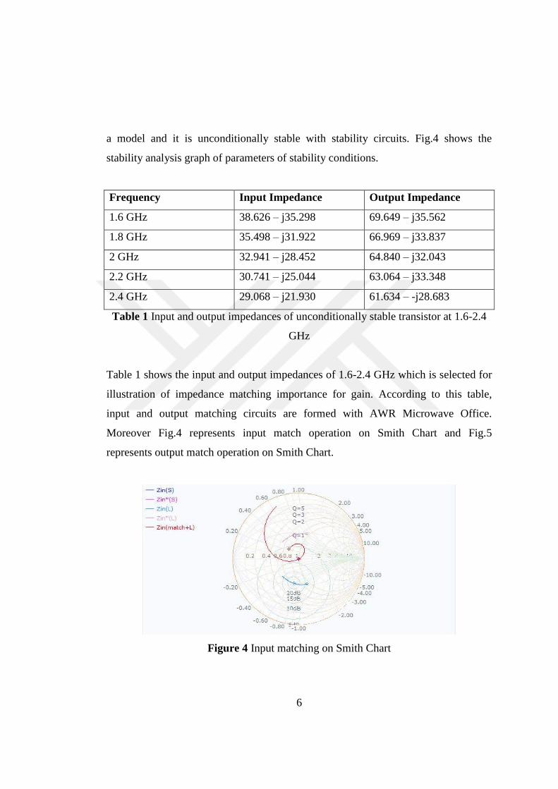
a model and it is unconditionally stable with stability circuits. Fig.4 shows the
stability analysis graph of parameters of stability conditions.
Frequency Input Impedance Output Impedance
1.6 GHz 38.626 – j35.298 69.649 – j35.562
1.8 GHz 35.498 – j31.922 66.969 – j33.837
2 GHz 32.941 – j28.452 64.840 – j32.043
2.2 GHz 30.741 – j25.044 63.064 – j33.348
2.4 GHz 29.068 – j21.930 61.634 – -j28.683
Table 1 Input and output impedances of unconditionally stable transistor at 1.6-2.4
GHz
Table 1 shows the input and output impedances of 1.6-2.4 GHz which is selected for
illustration of impedance matching importance for gain. According to this table,
input and output matching circuits are formed with AWR Microwave Office.
Moreover Fig.4 represents input match operation on Smith Chart and Fig.5
represents output match operation on Smith Chart.
Figure 4 Input matching on Smith Chart
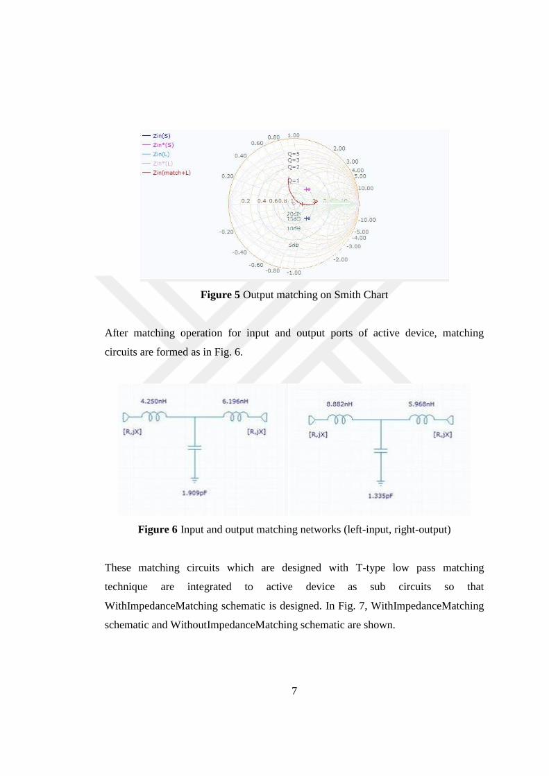
7
Figure 5 Output matching on Smith Chart
After matching operation for input and output ports of active device, matching
circuits are formed as in Fig. 6.
Figure 6 Input and output matching networks (left-input, right-output)
These matching circuits which are designed with T-type low pass matching
technique are integrated to active device as sub circuits so that
WithImpedanceMatching schematic is designed. In Fig. 7, WithImpedanceMatching
schematic and WithoutImpedanceMatching schematic are shown.

8
Figure 7 WithImpedanceMatching and WithoutImpedanceMatching circuit
schematics
Transistor available gain which is calculated with reference to its S-parameters for its
entire operating frequency band and results are expressed with
WithoutImpedanceMatching line. Other side, WithImpedanceMatching line shows
available gain for 1.6-2.4 GHz band. Therefore, unmatched circuits decrease gain of
network. Fig.8 which is explicitly explained impedance matching network function.
.

9
Figure 8 Comparison between matched and unmatched network
The following parameters and equations to design and analysis microwave transistor
amplifier are defined in detail in literature [2, 3] :
Γin (gamma_in) and Γout (gamma_out) as shown in Fig.1 express respectively
reflection coefficients measured from input port to device and from output port to
device.
Γin= S11+S12S21ΓL
1-S22ΓL and Γout= S22+
S12S21ΓS
1-S11ΓS (1.8)
ΓL=ZL-Z0
ZL+Z0 and ΓS=
ZS-Z0
ZS+Z0 (1.9)
Z0 is the characteristic impedance of the two port network. Source and load
reflection coefficients which are found with solution of Eq.1.9 are also parameters of
Eq.1.8.
𝐺𝑇 transducer power gain, 𝐺𝑃 the power gain (also called operating power gain) and
𝐺𝐴 are called as following equations:

10
GT=PL
PAVS=
power delivered to the load
power available from the source (1.10)
GP=PL
PIN=
power delivered to the load
power input to the network (1.11)
GA=PAVN
PAVS=
power available from the network
power available from the source (1.12)
Moreover, one of the most important requirements is stability analysis to design
without oscillations throughout operating frequency band [8, 9]. If Rollet’s condition
and auxiliary condition is provided, amplifier will be unconditionally stable [3, 9]. K
and Δ parameters, also their test condition to ensure unconditional stability are
defined as below equations [3, 9] :
K= 1-|S11|2-|S22|2+|Δ|2
2|S12S21| > 1 (1.13)
|Δ|= |S11S22-S12S21|<1 (1.14)
A single parameter µ has been defined in Ref. [8] for unconditionally stable two or
more networks and its condition is followed as:
µ=1- |S11|2
|S22-ΔS11* |+|S12S21|
>1 (1.15)
As a result, if µ > 1, the transistor is unconditionally stable. In design process, µ will
be investigated through whole frequency band for source and load.

11
1.4 Organization of the Thesis
This thesis is divided into five chapters. All studies include microwave transistor
amplifier analysis and design techniques. Especially, broadband distributed amplifier
technique is investigated and example designs are analyzed.
Chapter 1 consists of introduction with general explanation, microwave amplifier
main parameters, impedance matching and design equations belong to common
theory for microwave transistor amplifier.
Chapter 2 involves broadband design approaches and basically distributed amplifier
theory and its equations.
In Chapter 3, distributed amplifier design requirements and its analytical analysis
also, design process is investigated in detail.
In Chapter 4, conventional single stage distributed amplifier at 1-3 GHz frequency
band and cascaded single stage distributed amplifier are designed and their
simulation results are evaluated.
Chapter 5 is the conclusion part which involves comparisons between designed
distributed amplifiers according to gain, noise figure and return losses according to S
parameters.

12
CHAPTER 2
BROADBAND AMPLIFICATION
2.1 Overview of Broadband Amplifiers
Common design methods of broadband amplifiers to obtain more bandwidth are
briefly mentioned in this chapter. Moreover, distributed amplification as proposed
method is discussed. In literature, many works have done to increase bandwidth and
gain in order to cover demand high data rate and capacity in different frequency
bands for different applications and standards.
For 1-13 GHz bandwidth, Traveling-Wave Amplifier [10] approach was
implemented with GaAs FET and 9 dB±1dB gain was obtained. Another study from
literature [11] demonstrated four-cascaded single stage distributed amplifier
(CSSDA) by using HJ-FET as an active device with internal characteristic
impedance consideration and achieved 36.7±1 dB gain in 1-10 GHz bandwidth.
Finally, one of the important configurations from the literature is cascaded reactively
terminated single stage distributed amplifier (CRTSSDA) for 2-18 GHz operating
frequency range. In this paper [12], a solution was investigated to improve gain
performance of distributed amplifier configurations.
2.2 Methods of Broadband Amplifiers
According to Pozar [9], |𝑆21| decreases with at the rate of 6 dB/octave so broadband
matching networks require corresponding different 𝑆21 parameters versus operating
frequency band. Fundamentally, gain-bandwidth amplifier design [3] comprises

13
some difficulties as a result of the fact that some common methods are improved to
overcome complexities. They are listed as:
Compensating Matching (Lossy Matched):
Compensating matching technique is also implied lossy matched in literature. To aim
is compensating the variation of |𝑆21| in inversely proportion to frequency. As the
operating frequency increases the magnitude of 𝑆21 (gain performance) decreases by
reason of transistor characterization [13].
It is mentioned in this paper [14], lossy matched amplifier is similar with L-C
matched amplifier at high frequencies and C-R coupled amplifier at low frequencies.
L-C components do not have effect at low frequencies in a similar manner; R-C
coupling effect is negligible at high frequencies [14]. Another lossy matched circuit
configuration includes resistances.
Figure 9 Lossy matched amplifier topology (given in [15])
Fig.9 represents a basic circuit diagram which uses R1 and R2 resistors respectively
for input port and output port. These resistances provide gain-flatness over operating
frequency thanks to high attenuation at low frequencies and low attenuation at high
frequencies [15].
14
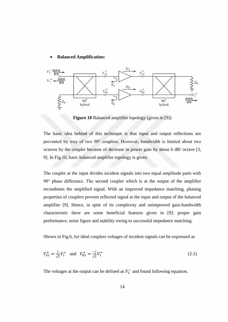
Balanced Amplification:
Figure 10 Balanced amplifier topology (given in [9])
The basic idea behind of this technique is that input and output reflections are
prevented by way of two 90° couplers. However, bandwidth is limited about two
octaves by the coupler because of decrease in power gain by about 6 dB/ octave [3,
9]. In Fig.10, basic balanced amplifier topology is given.
The coupler at the input divides incident signals into two equal amplitude parts with
90° phase difference. The second coupler which is at the output of the amplifier
recombines the amplified signal. With an improved impedance matching, phasing
properties of couplers prevent reflected signal at the input and output of the balanced
amplifier [9]. Hence, in spite of its complexity and unimproved gain-bandwidth
characteristic there are some beneficial features given in [9]: proper gain
performance, noise figure and stability owing to successful impedance matching.
Shown in Fig.6, for ideal couplers voltages of incident signals can be expressed as
𝑉𝐴1+ =
1
√2𝑉1
+ and 𝑉𝐵1+ =
−𝑗
√2𝑉1
+ (2.1)
The voltages at the output can be defined as 𝑉2− and found following equation.

15
𝑉2− =
−𝑗
√2𝑉𝐴2
+ +1
√2𝑉𝐵2
+ =−𝑗
√2𝐺𝐴𝑉𝐴1
+ + 1
√2𝐺𝐵𝑉𝐵1
+ (2.2)
Where 𝐺𝐴 and 𝐺𝐵 is the gain of amplifiers respectively A and B and output voltage
can be written briefly as
𝑉2− =
−𝑗
2𝑉1
+(𝐺𝐴 + 𝐺𝐵) (2.3)
𝑆21 extracted from equation (2.3) which represents the gain of whole balanced
amplifier can be written as
𝑆21 = 𝑉2
−
𝑉1+ =
−𝑗
2(𝐺𝐴 + 𝐺𝐵) (2.4)
When amplifiers are identical in other words 𝐺𝐴 = 𝐺𝐵 and 𝛤𝐴 = 𝛤𝐵 (reflection
coefficients are equal) [9]. This is a special case and figures 𝑆11 = 0 so that perfectly
matched couplers are obtained in balanced amplifier design [9].
Feedback Amplification :
Niclas, et al. [16] is mentioned that parasitic elements of active devices limit the
bandwidth of amplifier. Feedback amplifier is developed to minimize these effects
on extension bandwidth [16] and this topology was proposed in this paper.
16
Figure 11 Feedback amplifier topology (given in [15])
Lfb , Cfb and Rfb are the elements of feedback topology which is shown in Fig. 11.
𝐿𝑓𝑏 can define the operating frequency with drain and gate lines inductance. Its
adjustments provide flat gain while increasing frequency. Another component of
feedback route is Cfb which eliminates DC biasing effects on gate and drain lines.
Feedback resistance is obtained 𝑅𝑓𝑏 which decreases gain at lower frequencies and
designates the gain and bandwidth of the amplifier [15]. Feedback resistor 𝑅𝑓𝑏 can
also be used alone in hybrid topologies to obtain gain-flatness.
The last broadband amplification method is distributed amplification which is used in
this thesis designed amplifier. It will be explained in next section.
2.3 Distributed Amplification
Thermionic valve circuit was described to obtain voltage amplification by Percival
[17] and his invention is based on using an amplifying path to bypass cathode
follower valve in wide frequencies. In other words, he described [17] that input
circuit capacitance and resistance of the valve defines the bandwidth. Thereafter,
Ginzton [18] named this new amplification technique (theory) as distributed
amplification and defined basic principles of distributed amplification. The traveling-
wave concept was followed in his design and a new technique was developed for

17
wide band amplifiers at both low frequencies and microwaves [18]. Fundamental
idea of this configuration is that two artificial transmission lines are designed by
absorbing tube capacitances [18]. Therefore, transmission lines overcome the
challenge which capacitances of active device bound the bandwidth of amplifier.
In development process of distributed amplification techniques, BJTs and FETs are
used for many studies in literature. Jutzi [19] designed 2 GHz bandwidth distributed
amplifier with MESFETs and in this study characteristic impedances of lines are
chosen as 50Ω. In this configuration, approximately 6 dB gain was obtained and
noise figure was between 5 - 7 dB at nearly 2 GHz. Afterwards, a monolithic GaAs
FET traveling-wave amplifier at 1-13 GHz operating frequency band was designed
and manufactured [10]. Ayasli [10] showed that increase in active device (transistor)
did not increase the gain also; gain performance got near zero with large number of
stages on the contrary early conventional amplifiers theories. New insights have been
provided to broadband microwave amplifier world with developed new transistors.
Moreover, power added efficiency (PAE) and gain flatness have increased in
distributed amplification with these new insights.
The basic configuration of conventional distributed amplifier with N identical FETs
is shown in Fig. 12. At the same time, configuration in this figure works in a special
case which is unilateral version (𝐶𝑔𝑑 = 0) [9]. Their gate and drain poles are
connected to separate terminated artificial transmission lines which have
characteristic impedances respectively Zg and Zd [9]. Artificial transmission lines
may be formed of both lumped elements and micro strip lines. Transmission lines
absorb the input and output capacitances of transistor and the bandwidth of this
configuration is determined by the transmission line.

18
Figure 12 Basic diagram of N-stage distributed amplifier (given in [9])
DA equations and principles will be discussed in next chapter in detail. Moreover,
using DA technique 1-3 GHz (L-S Band) will be designed with AWR microwave
Office CAD tool and stages of design process will be explained. After that,
simulation results and main parameters of the amplifier will be evaluated.
19
CHAPTER 3
ANALYSIS OF THE DISTRIBUTED AMPLIFIER
3.1 Principles of Distributed Amplifier
Distributed amplifier is known as one of the most common and well-established
broadband amplifier techniques [20] owing to high wideband performance, low
voltage standing wave ratio (VSWR) over operation frequency range, noise figure
and low cost.
Cut off frequency is defined by inductance of artificial transmission lines and gate to
source capacitor 𝐶𝑔𝑠 of the transistor [20]. If gate to source capacitor value is high,
cut off frequency will be low.
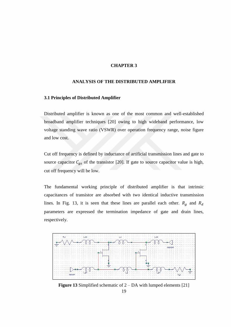
The fundamental working principle of distributed amplifier is that intrinsic
capacitances of transistor are absorbed with two identical inductive transmission
lines. In Fig. 13, it is seen that these lines are parallel each other. 𝑅𝑔 and 𝑅𝑑
parameters are expressed the termination impedance of gate and drain lines,
respectively.
Figure 13 Simplified schematic of 2 – DA with lumped elements [21]

20
The basic concept of conventional distributed amplifier is paralleling number of
ideally similar transistor with connected two artificial transmission lines. These lines
have the constant characteristic impedances as Zg for gate line and Zd for drain line
and they are matched with the characteristic impedance of whole circuit Z0. Their
strategy is that the gate to source capacitance 𝐶𝑔𝑠of the transistor regarded as input
capacitance is a part of the transmission lines and cancelled with the inductive
artificial lines. It is similar with for output capacitance. In shown Fig. 14, basic
configuration of conventional distributed amplifier works as a RF input travelling
from left to right and terminating with a resistance circuit.
Amplifying process in this configuration begins at first stage with a RF input going
out from the gate of transistor and traveling from the left to right and at the end of
line terminating in a resistance and biased circuit. Then, a portion of amplified signal
at the drain of transistor wants to travel right and another portion of the signal wants
to travel left. All other stages are similar with the first stage. It is considered in this
working principle that transmission lines are adjusted signals at opposite direction
cancelling each other at the interstage of the transistor. It is not perfectly matched yet
reasonably close. Hence, backward waves are not considered.
Figure 14 Basic concept of conventional distributed amplifier

21
3.2 Analytical Analysis of Distributed Amplifier
Pozar [9] analyzed N-stage conventional distributed amplifier theory analytically.
Fig.15 shows equivalent circuit for unit stage of the gate line. Zg is defined as
characteristic impedance of the gate line and Lg expresses the whole gate line length,
𝑙𝑔 means per unit length [9]. 𝑅𝑖 is the input resistance of FET, according to
Advanced Curtice-2 Die Model it is defined as gate to source resistance as well.
Also, parasitic elements in this die model of ATF-54143 transistor are used in the
thesis.
Figure 15 The equivalent circuit of a single unit cell of the gate line [9]
Z=jwLg (3.1)
𝑌 = 𝑗𝑤𝐶𝑔 +
𝑗𝑤𝐶𝑔𝑠𝑙𝑔
⁄
1+𝑗𝑤𝑅𝑖𝐶𝑔𝑠 (3.2)
Impedance of the gate line and shunt admittance per unit length [9] is expressed with
respectively equations (3.1) and (3.2).
22
Assuming loss neglected, characteristic impedance can be written as
Zg=√Z
Y= √
Lg
Cg+ Cgs/lg (3.3)
When formulating of propagation constant, attenuation will be originated by resistive
term by reason of attenuation.
𝛾𝑔 = ɑ𝑔 + 𝑗𝛽𝑔 = √𝑍𝑌 = √𝑗𝑤𝐿𝑔 (𝑗𝑤𝐶𝑔 +
𝑗𝑤𝐶𝑔𝑠
𝑙𝑔
1+𝑗𝑤𝑅𝑖𝐶𝑔𝑠) (3.4)
If small loss is assumed, 𝑤𝑅𝑖𝐶𝑔𝑠 ≪ 1 is obtained and above equation is arranged as
𝛾𝑔 = ɑ𝑔 + 𝑗𝛽𝑔 ≅ √−𝑤2𝐿𝑔[𝐶𝑔 + 𝐶𝑔𝑠(1 − 𝑗𝑤𝑅𝑖𝐶𝑔𝑠)/𝑙𝑔]
≅ 𝑤2𝑅𝑖𝐶𝑔𝑠
2 𝑍𝑔
2𝑙𝑔+ 𝑗𝑤√𝐿𝑔(𝐶𝑔 + 𝐶𝑔𝑠/𝑙𝑔) (3.5)
Figure 16 The equivalent circuit of a single unit cell of the drain line [9]

23
Fig.16 shows equivalent circuit for unit stage of the drain line which is similar with
gate line, characteristic impedance of drain line and shunt admittance per unit length
are calculated as
𝑍 = 𝑗𝑤𝐿𝑑 (3.6)
𝑌 = 1
𝑅𝑑𝑠𝑙𝑑+ 𝑗𝑤(𝐶𝑑 + 𝐶𝑑𝑠/𝑙𝑑) (3.7)
𝑍𝑑 = √𝑍
𝑌= √
𝐿𝑑
𝐶𝑑+ 𝐶𝑑𝑠/𝑑 (3.8)
Propagation constant of the drain line is expressed with some negligence as
𝛾𝑑 = ɑ𝑑 + 𝑗𝛽𝑑 = √𝑍𝑌 = √𝑗𝑤𝐿𝑑 (1
𝑅𝑑𝑠𝑙𝑑+ 𝑗𝑤(𝐶𝑑 + 𝐶𝑑𝑠/𝑙𝑔)) (3.9)
≅ 𝑍𝑑
2𝑅𝑑𝑠𝑙𝑑+ 𝑗𝑤√𝐿𝑑(𝐶𝑑 + 𝐶𝑑𝑠/𝑙𝑑) (3.10)
Phase differences are not considered in distributed amplification owing to 𝛽𝑔𝑙𝑔 =
𝛽𝑑𝑙𝑑 condition [9, 10] and this is obtained thanks to equal transmission lines. It is
assumed that drain and gate line impedances are approximately equal the
characteristic impedance. Hence, it is written gain equation in a simple way.
𝐺 =𝑃𝑜𝑢𝑡
𝑃𝑖𝑛=
𝑔𝑚2 𝑍𝑑𝑍𝑔
4
(𝑒−𝑁𝑎𝑔𝑙𝑔−𝑒−𝑁𝑎𝑑𝑙𝑑)2
(𝑒−𝑎𝑔𝑙𝑔−𝑒−𝑎𝑑𝑙𝑑)2 (3.11)
Because of 𝑍𝑑 = 𝑍𝑔 and, small divider part of equation (3.11) gain is written as
24
𝐺 = 𝑔𝑚
2 𝑍𝑑𝑍𝑔𝑁2
4 (3.12)
𝑁𝑜𝑝𝑡 = 𝑙𝑛(𝑎𝑔𝑙𝑔/𝑎𝑑𝑙𝑑)
𝑎𝑔𝑙𝑔−𝑎𝑑𝑙𝑑 (3.13)
Number of stages depend on the losses in the amplifier gate and drain line, so when
the number of transistors is in increase gain approaches to zero [9, 10]. Starting
travel from the gate to drain input signal attenuated each line and amplified signal
cannot come in the output at the last drain pole if the number of transistor approaches
infinity [9, 10]. The most optimal number of transistors is calculated with equation
(3.13).
3.3 About Transistors Used in Case Study
Avago Technologies ATF-54143 model transistor which has Low Noise
Enhancement Mode Pseudomorphic High Electron Mobility Transistor (E-PHEMT)
technology is used in the thesis for all analyses and designs. Operation frequency
range of ATF-54143 is 450 MHz to 6 GHz. Common usage fields are low noise
applications [22]. It is preferred since less noisy design is obtained.
It is biased with 3.6 V from drain and gate poles. Transistor operating conditions are
chosen 𝑉𝑑𝑠 = 3𝑉 and 𝐼𝑑𝑠 = 60 𝑚𝐴 for case studies. At 2 GHz frequency, 3V and 60
mA noise figure 0.5 dB, associated gain is 16.6 are stated in datasheet of ATF-54143
[22]. Also, advanced curtice-2 die model and scattering parameters according to
chosen bias condition are presented at appendices section. Moreover, transistor 𝐶𝑔𝑠
gate to source capacitance value is 1.73 pF and 𝐶𝑑𝑠 drain to source capacitance value
is 0.27 pF. These intrinsic capacitances of transistor is defined inductive artificial
transmission line parameters according to cut off frequency in distributed amplifier
design procedures.

25
3.4 Stability Analysis
Stability is one of the most important requirements for designing amplifier. It is
analyzed to prevent low-frequency oscillations because of internal, external and
thermal feedback [23]. Conditionally stable and unstable active devices have
negative effects on amplifier such as gain performance, noise figure and efficiency.
To overcome these problems, Rollet’s condition and auxiliary condition is applied
with using equations (1.11) and (1.12). In this design, stability analysis is done by
help of CAD tool.
Figure 17 Stability analysis of ATF-54143 at operating frequency range for
Vds=3V and Ids=60 mA
Fig. 17 shows that transistor is not unconditionally stable at determined conditions
and operating frequency of so stability circuit is added to provide unconditionally
stability for the designed amplifier. This circuit generally comprises of a resistor and
a capacitor like Fig. 18; so that electrical behavior of transistor is improved as
unconditionally stable.

26
Figure 18 Stability circuit schematic
After the connection of stability circuit which is represented in Fig.18 to active
device, unconditionally stability requirements are fulfilled. According to the results
of Stability Analysis graph, stability circuit is designed and optimized. Stability
Check graph is obtained with using 22 Ω resistors and 2 pF capacitors. All stability
parameters are bigger than 1 so, transistor is unconditionally stable.
Figure 19 Stability analysis after the connecting stability circuit
Stability circuit is provided unconditionally stability at amplifier operating frequency
range which is 1-3 GHz and as seen in Fig. 19.

27
3.5 Bias Circuit of Used Transistor
In the thesis, passive biased circuit is designed with 3.6V supply. Vds=3V and
Ids=60 mA biasing condition is made up. Fig. 16 shows bias circuit schematic of the
design amplifier in case study. In this bias circuit, Vds=3V and Ids=62.4 mA is
measured from analyzing on AWR Microwave Office.
Figure 20 Bias circuit schematic
For microwave amplifiers, there are several configurations to design bias network
and voltage divider bias technique is used to design bias circuit and simulation
results are also given Fig.20. Moreover, ATF-54143 is defined with CURTICE2
Model and its die model parameters are given at APPENDIX A.

28
3.6 Input and Output Matching Circuits
Impedance matching is a way to transfer maximum power from the source to the
load. Impedance matching network are designed by conjugate matching reflection
coefficients of source and load with input and output reflection coefficients of the
active device [3, 9] to obtain the maximum gain stable single stage transistor
amplifier. To calculate these reflection coefficients for simultaneous conjugate match
some formulas are defined as:
𝛤𝑠 = 𝐵1±√𝐵1
2−4|𝐶1|2
2𝐶1 (3.14)
𝛤𝐿 = 𝐵2±√𝐵2
2−4|𝐶2|2
2𝐶2 (3.15)
Above equations express reflection coefficient of source and load and variables used
in (3.14) and (3.15) is found with following formulas.
𝐵1 = 1 + |𝑆11|2 − |𝑆22|2 − |∆|2 (3.16)
𝐵2 = 1 + |𝑆22|2 − |𝑆11|2 − |∆|2 (3.17)
𝐶1 = 𝑆11 − ∆𝑆22∗ (3.18)
𝐶2 = 𝑆22 − ∆𝑆11∗ (3.19)
𝛤𝑖𝑛 and 𝛤𝑜𝑢𝑡 are input and output matched circuit reflection coefficients of the
transistor. And they are equal conjugate of the source and load reflection coefficients
as defined with below equations.

29
𝛤𝑖𝑛 = 𝛤𝑠∗ and 𝛤𝑜𝑢𝑡 = 𝛤𝐿
∗ (3.20)
Conjugate matching approach is the optimum matching technique for narrowband
single stage transistor amplifier to transfer maximum power from source to load.
However, matching networks may not cover whole frequency band for broadband
amplifiers. If the impedances are close to each other, center frequency can be chosen
by using equation (3.21) and then matching circuit elements can be optimized to
increase available gain of amplifier.
It is required that matching network covers whole bandwidth with minimum
reflection coefficient [23], and this is a problem to solve. By Bode-Fano criterion, to
approach optimum matching network requirements are defined [23]. According to
that criterion, center frequency of lossless matching network versions [23] is
calculated as:
𝑓0 = √𝑓𝐿𝑓𝐻 (3.21)
𝑓0 is the center frequency between high and low cut off frequencies. This equation is
simplified from
𝑤0 = √𝑤𝐿𝑤𝐻 (3.22)
It is required that matching network covers whole bandwidth with minimum
reflection coefficient [23], and this is a problem to solve. By Bode-Fano criterion, to
approach optimum matching network requirements are defined [23].
In the thesis, matching networks are design with CAD tools with bandpass filtering
and bandpass impedance matching methods. By using (3.21) and (3.22) center

30
frequency is calculated with 1 GHz low frequency and 3 GHz high frequency. As a
result center frequency is found approximately 1.7 GHz. For 1-3 GHz frequency
range center frequency is approximately 1.7 GHz yet, matching circuits are designed
center frequency based on 2 GHz since gain performance is higher at low frequencies
then at high frequencies because of transistor characteristic. Hence, center frequency
is chosen closer to high cut off frequency.
Frequency Input Impedance Output Impedance
1 GHz 7.764 - j49.854 8.371 - j1.979
1.25 GHz 5.445 - j39.617 8.192 - j1.801
1.5 GHz 4.175- j32.610 8.051 - j1.665
1.75 GHz 3.407 - j27.487 7.940 - j1.556
2 GHz 2.908 - j23.558 7.854 - j1.468
2.25 GHz 2.566 - j20.430 7.786 - j1.397
2.5 GHz 2.323 - j17.866 7.732 - j1.341
2.75 GHZ 2.144 - j15.715 7.689 - j1.295
3 GHz 2.010 - j13.873 7.653 - j1.260
Table 2 Input and output impedances of biased circuit for impedance matching
circuits
Figure 21 Input matching on Smith Chart

31
In Fig. 21 and Fig. 22 shows input and output matching studies on Smith Chart.
Figure 22 Output matching on Smith Chart
Fig. 23 represents input and output matching circuits for center frequency 2 GHz
respectively. The left schematic shows the input matching circuit and the right
schematic shows the output matching circuit.
Figure 23 Input and output impedance matching circuits (left -input matching, right
–output matching)

32
CHAPTER 4
DESIGN OF DISTRIBUTED AMPLIFIER
4.1 Design and Simulation Results of Conventional Single Stage Distributed
Amplifier
In previous chapter, it is mentioned that the significant point of the distributed
amplification is absorbing internal parasitic capacitances at the transistor [25]. There
are two artificial transmission lines are required to realize the main principle of
distributed amplification. Also, input and output capacitances of the transistor with
gate and drain transmission lines are matched to characteristic impedance with
following equations.
𝑓𝑐 ≅1
𝜋√𝐿𝐶 (3.23)
𝑍0 = √𝐿/𝐶 (3.24)
When cut off frequency is defined, inductor value of the transmission line can be
calculated by using equation (3.23). After that, according to characteristic impedance
by using equation (3.24) capacitance value is found and T type or L type artificial
line can be designed [25]. T type and L type transmission lines are designed for the
gate in this single stage conventional distributed amplifier. Therefore, transistor is
included as a part of 50 Ω system with inductive artificial transmission lines. Thanks
to these principles of distributed amplification operation frequency band is increased
for broadband amplifiers.
33
Calculations for Conventional SSDA:
DA configuration of ATF-54143 transmission line has 50 Ω characteristic impedance
cut off frequency can be written as [23]
𝑓𝑐 =1
𝜋𝑍0𝐶𝑔𝑠 (3.25)
According to principles of distributed amplification concept cut off frequency is
determined 3 GHz and by using equation (3.23)
𝑓𝑐 ≅1
𝜋√𝐿𝐶≅ 3 𝐺𝐻𝑧 ≅ 3𝑥109 𝐻𝑧
C represents 𝐶𝑔𝑠 (gate to source) parameter of transistor and its value is 1.73 pF.
3𝑥109 ≅1
𝜋√𝐿𝑥1.73𝑥10−12
9𝑥1018 ≅1
𝜋2𝑥𝐿𝑥1.73𝑥10−12
𝐿 =10−6
9𝑥1.73𝑥𝜋2 = 6.50𝑥10−9𝐻
Inductor value of artificial transmission lines is found 6.5 nH from calculations.
After that, L/2 value is found as 3.25 nH.
Capacitance value which is used in T type and L type transmission lines is calculated
to provide matching with system characteristic impedance as 50 Ω by following
equation (3.24).
34
50 = √6.5 𝑛𝐻/𝐶
2500 =6.5𝑥10−9
𝐶
𝐶 =6.5𝑥10−11
25= 2.6𝑥10−12
Capacitance value of matching part is calculated as 2.6 pF.
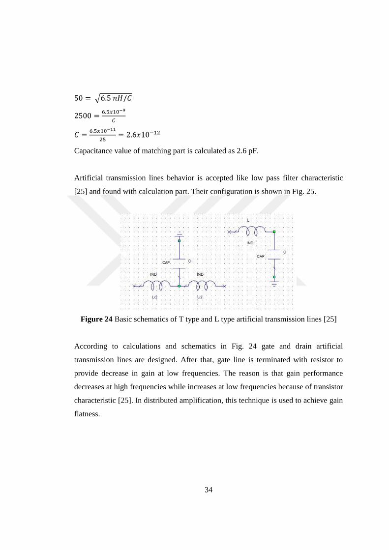
Artificial transmission lines behavior is accepted like low pass filter characteristic
[25] and found with calculation part. Their configuration is shown in Fig. 25.
Figure 24 Basic schematics of T type and L type artificial transmission lines [25]
According to calculations and schematics in Fig. 24 gate and drain artificial
transmission lines are designed. After that, gate line is terminated with resistor to
provide decrease in gain at low frequencies. The reason is that gain performance
decreases at high frequencies while increases at low frequencies because of transistor
characteristic [25]. In distributed amplification, this technique is used to achieve gain
flatness.

35
Figure 25 Conventional single stage distributed amplifier schematic
As seen in Fig. 25, gate and drain artificial transmission lines are integrated with
biased active device according to results of calculations for conventional distributed
amplifier. Also, gate artificial transmission line is terminated with resistance to
decrease gain performance at low frequencies. Simulation of available gain is shown
in Fig. 26. At design frequency range, gain is changeable between approximately
14.3 and almost 8.9 dB. At the end of operation frequency band available gain is
dramatically decreased.

36
Figure 26 Available gain single stage distributed amplifier
Single stage distributed amplifier gain performance is affected from drawn equal
transmission lines for gate and drain port of transistor and selected cut off frequency
to obtain gain flatness at 1-3 GHz operation frequency band. Moreover, cut off
frequency is selected as the end of frequency band 3 GHz and this leads to dramatic
decrease in available gain so, in next section cut off frequency is moved to right to
prevent dramatic decrease in gain at the end of frequencies.

37
Figure 27 S parameters in logarithmic magnitude (in dB) of conventional SSDA
S parameters in logarithmic magnitude gives information about input return loss,
output return loss and gain. In Fig. 27, S parameters simulation is shown. Input
return loss value is almost -8.9 dB at the beginning of frequency band and
approximately -0.5 dB at the end of the frequency band as seen in Fig. 27. If input
and output return loss value is low, losses are low in amplifier. Output return loss
line is starting from -4 dB at 1 GHz and it is in increase almost to -0.0.7 dB at 3GHz.
According to, gain performance simulations of drawn conventional single stage
distributed amplifier schematic conjugate matched circuits are integrated to
investigate gain performances. Impedance matching circuit consists of conjugate
matched to input reflection coefficient of transistor as regards center frequency of
bandwidth similar with narrowband amplification impedance matching technique.
This analysis is followed for conventional distributed amplifier as a different point of
view.
38
Frequency Input Impedance Output Impedance
1 GHz 7.764 - j49.854 8.371 - j1.979
1.5 GHz 4.175- j32.610 8.051 - j1.665
2 GHz 2.908 - j23.558 7.854 - j1.468
2.5 GHz 2.323 - j17.866 7.732 - j1.341
3 GHz 2.010 - j13.873 7.653 - j1.260
Table 3 Input and output impedances of biased circuit at 1-3 GHz
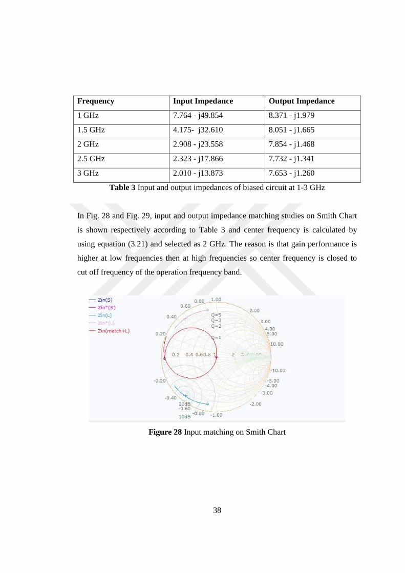
In Fig. 28 and Fig. 29, input and output impedance matching studies on Smith Chart
is shown respectively according to Table 3 and center frequency is calculated by
using equation (3.21) and selected as 2 GHz. The reason is that gain performance is
higher at low frequencies then at high frequencies so center frequency is closed to
cut off frequency of the operation frequency band.
Figure 28 Input matching on Smith Chart
39
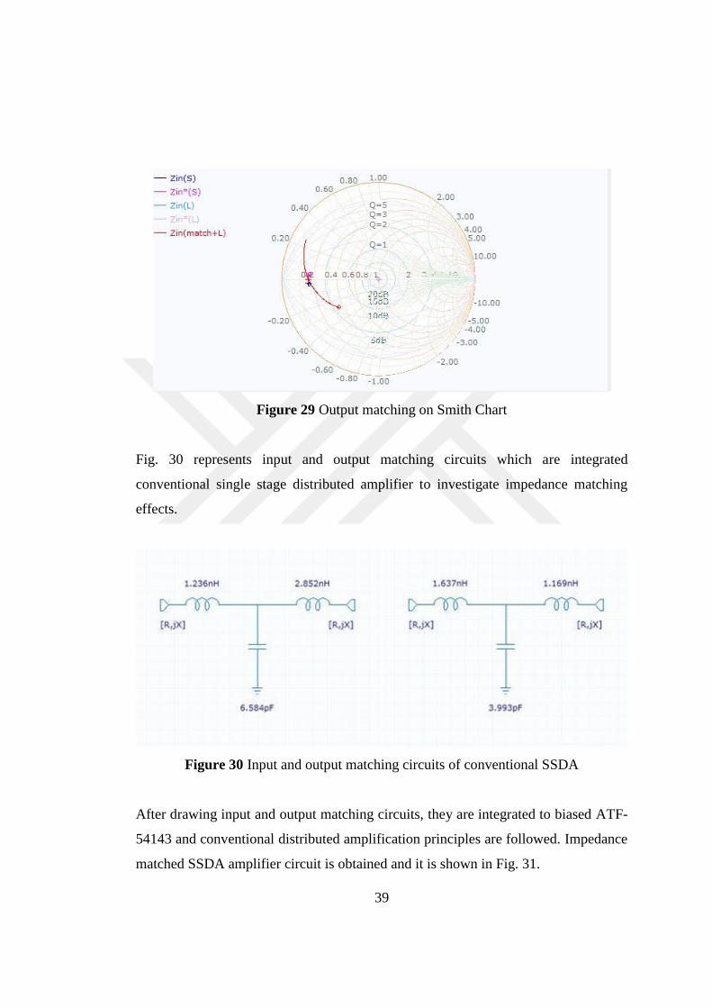
Figure 29 Output matching on Smith Chart
Fig. 30 represents input and output matching circuits which are integrated
conventional single stage distributed amplifier to investigate impedance matching
effects.
Figure 30 Input and output matching circuits of conventional SSDA
After drawing input and output matching circuits, they are integrated to biased ATF-
54143 and conventional distributed amplification principles are followed. Impedance
matched SSDA amplifier circuit is obtained and it is shown in Fig. 31.
40
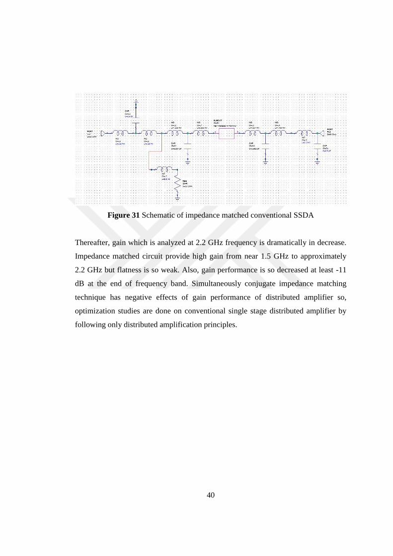
Figure 31 Schematic of impedance matched conventional SSDA
Thereafter, gain which is analyzed at 2.2 GHz frequency is dramatically in decrease.
Impedance matched circuit provide high gain from near 1.5 GHz to approximately
2.2 GHz but flatness is so weak. Also, gain performance is so decreased at least -11
dB at the end of frequency band. Simultaneously conjugate impedance matching
technique has negative effects of gain performance of distributed amplifier so,
optimization studies are done on conventional single stage distributed amplifier by
following only distributed amplification principles.

41
Figure 32 Available gains of SSDA and impedance matched SSDA
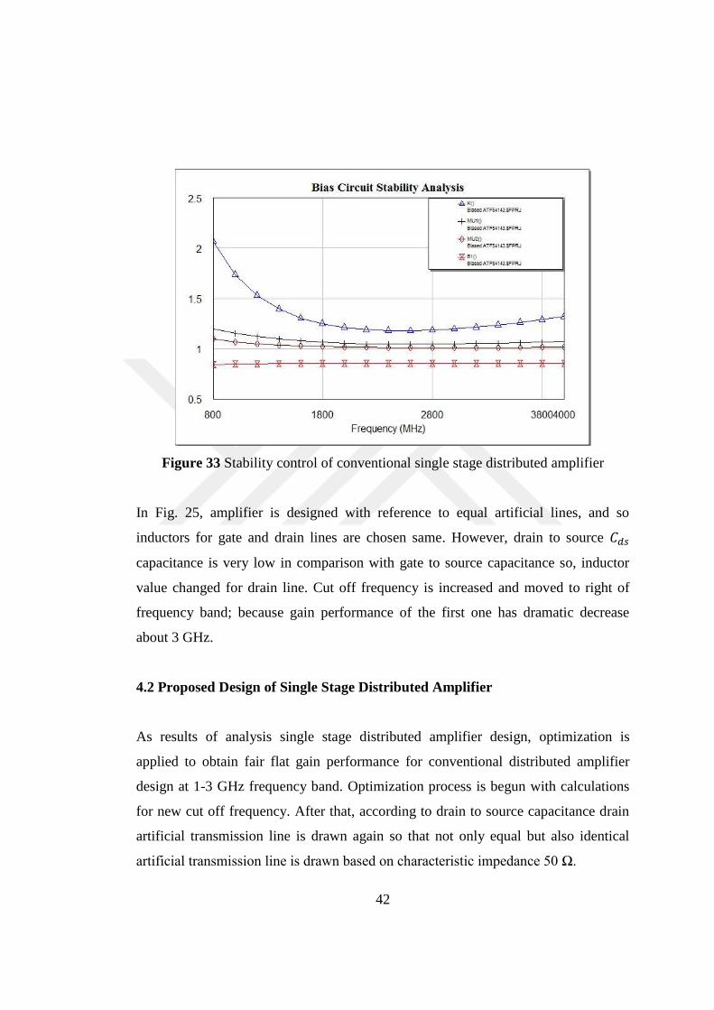
It is mentioned before section 3.4 Stability Analysis; stability of conventional SSDA
is controlled and is observed in Fig. 33. K parameter is in Rollet’s condition, and B1
represents auxiliary condition to analyze unconditional stability. Other parameters of
stability analysis are MU1 and MU2 which represent µ tests for source and load ports
respectively.
42
Figure 33 Stability control of conventional single stage distributed amplifier
In Fig. 25, amplifier is designed with reference to equal artificial lines, and so
inductors for gate and drain lines are chosen same. However, drain to source 𝐶𝑑𝑠
capacitance is very low in comparison with gate to source capacitance so, inductor
value changed for drain line. Cut off frequency is increased and moved to right of
frequency band; because gain performance of the first one has dramatic decrease
about 3 GHz.
4.2 Proposed Design of Single Stage Distributed Amplifier
As results of analysis single stage distributed amplifier design, optimization is
applied to obtain fair flat gain performance for conventional distributed amplifier
design at 1-3 GHz frequency band. Optimization process is begun with calculations
for new cut off frequency. After that, according to drain to source capacitance drain
artificial transmission line is drawn again so that not only equal but also identical
artificial transmission line is drawn based on characteristic impedance 50 Ω.
43
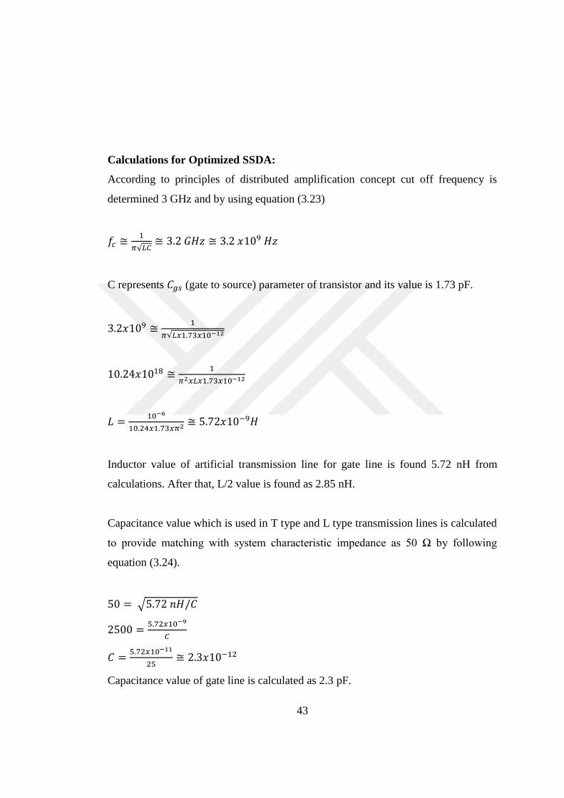
Calculations for Optimized SSDA:
According to principles of distributed amplification concept cut off frequency is
determined 3 GHz and by using equation (3.23)
𝑓𝑐 ≅1
𝜋√𝐿𝐶≅ 3.2 𝐺𝐻𝑧 ≅ 3.2 𝑥109 𝐻𝑧
C represents 𝐶𝑔𝑠 (gate to source) parameter of transistor and its value is 1.73 pF.
3.2𝑥109 ≅1
𝜋√𝐿𝑥1.73𝑥10−12
10.24𝑥1018 ≅1
𝜋2𝑥𝐿𝑥1.73𝑥10−12
𝐿 =10−6
10.24𝑥1.73𝑥𝜋2 ≅ 5.72𝑥10−9𝐻
Inductor value of artificial transmission line for gate line is found 5.72 nH from
calculations. After that, L/2 value is found as 2.85 nH.
Capacitance value which is used in T type and L type transmission lines is calculated
to provide matching with system characteristic impedance as 50 Ω by following
equation (3.24).
50 = √5.72 𝑛𝐻/𝐶
2500 =5.72𝑥10−9
𝐶
𝐶 =5.72𝑥10−11
25≅ 2.3𝑥10−12
Capacitance value of gate line is calculated as 2.3 pF.

44
C represents 𝐶𝑑𝑠 (gate to source) parameter of transistor and its value is 0.27 pF.
𝑓𝑐 ≅1
𝜋√𝐿𝐶≅ 3.2 𝐺𝐻𝑧 ≅ 3.2 𝑥109 𝐻𝑧
3.2𝑥109 ≅1
𝜋√𝐿𝑥0.27𝑥10−12
10.24𝑥1018 ≅1
𝜋2𝑥𝐿𝑥0.27𝑥10−12
𝐿 =10−6
10.24𝑥0.27𝑥𝜋2 ≅ 36.64𝑥10−9𝐻
Inductor value of artificial transmission line for drain line is found 36.64 nH from
calculations. After that, L/2 value is found as 18.3 nH. Capacitance value which is
used in T type and L type transmission lines is calculated to provide matching with
system characteristic impedance as 50 Ω by following equation (3.24).
50 = √36.64 𝑛𝐻/𝐶
2500 =36.64𝑥10−9
𝐶
𝐶 =36.64 𝑥10−11
25≅ 0.146𝑥10−12
Capacitance value of drain line is calculated as 0.146 pF.
According to calculations, conventional single stage distributed amplifier is
optimized and it is shown in Fig. 34.

45
Figure 34 Optimized single stage distributed amplifier
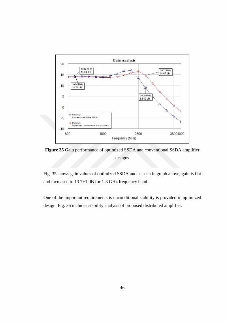
Gain analysis of optimized single stage distributed amplifier is shown in Fig. 35.
Available gain of optimized amplifier circuit is approximately 14 dB at the beginning
of frequency band and almost 14.7 dB at the end of frequency band. Gain is
increased in comparison with first amplifier and also flatness is obtained in the
selected operation frequency band.
46
Figure 35 Gain performance of optimized SSDA and conventional SSDA amplifier
designs
Fig. 35 shows gain values of optimized SSDA and as seen in graph above, gain is flat
and increased to 13.7+1 dB for 1-3 GHz frequency band.
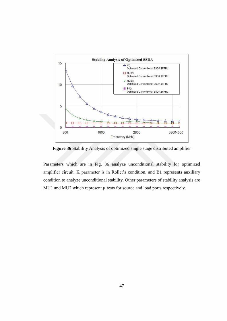
One of the important requirements is unconditional stability is provided in optimized
design. Fig. 36 includes stability analysis of proposed distributed amplifier.
47
Figure 36 Stability Analysis of optimized single stage distributed amplifier
Parameters which are in Fig. 36 analyze unconditional stability for optimized
amplifier circuit. K parameter is in Rollet’s condition, and B1 represents auxiliary
condition to analyze unconditional stability. Other parameters of stability analysis are
MU1 and MU2 which represent µ tests for source and load ports respectively.

48
Figure 37 S parameters (in dB) of optimized single stage distributed amplifier
S parameters in logarithmic magnitude gives information about input return loss,
output return loss and gain. In Fig. 28, S parameters simulation is shown. Input
return loss value is -9.4 dB at the beginning of frequency band and approximately
-2.5 dB at the end of the frequency band and minimum value is -9.4 dB near 1 GHz
as seen in Fig. 28. If input and output return loss value is low, losses are low in
amplifier. Output return loss line is starting from -0.14 dB at 1 GHz and it is in
increase to -0.11 dB at 3GHz.
Available gain is measured by increasing the number of stages. As a result, as the
stages increase, gain performance gets worse. When calculating optimum number of
transistor, equation (3.5) is used and result equals to 24 because of drain line
attenuation is bigger than the gate line attenuation.

49
4.3 2 – CASCADED Single Stage Distributed Amplifier
Cascaded Single Stage Distributed Amplifier (CSSDA) is based on conventional
distributed amplifier or traveling wave amplifier theory. Input signal goes into
transmission line and after amplified travel to the gate of second transistor. High gain
and gain flatness in bandwidth can be obtained with different configurations of
CSSDA.
Conventional distributed amplifier gain value is restricted because of optimum stages
of transistors. Hence, to obtain high gain and solve conventional distributed amplifier
configuration problems a new topology is developed as cascadable gain stages [27].
Series number of FETs are connected cascaded and their separate terminations of
gate and drain line brings a new concept to broadband amplification world [20].
Internal characteristic impedance is used the inner stages termination. Other side,
gate and drain stages are terminated with characteristic impedances of transmission
lines [20]. Also, every stage of the amplifier behaves like a T-type amplifier [20].
Figure 38 Designed 2-CSSDA schematic
50
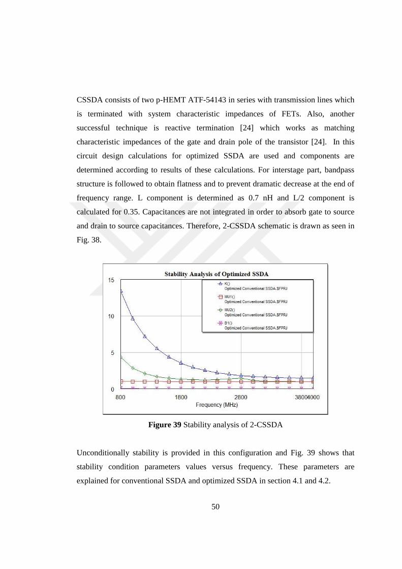
CSSDA consists of two p-HEMT ATF-54143 in series with transmission lines which
is terminated with system characteristic impedances of FETs. Also, another
successful technique is reactive termination [24] which works as matching
characteristic impedances of the gate and drain pole of the transistor [24]. In this
circuit design calculations for optimized SSDA are used and components are
determined according to results of these calculations. For interstage part, bandpass
structure is followed to obtain flatness and to prevent dramatic decrease at the end of
frequency range. L component is determined as 0.7 nH and L/2 component is
calculated for 0.35. Capacitances are not integrated in order to absorb gate to source
and drain to source capacitances. Therefore, 2-CSSDA schematic is drawn as seen in
Fig. 38.
Figure 39 Stability analysis of 2-CSSDA
Unconditionally stability is provided in this configuration and Fig. 39 shows that
stability condition parameters values versus frequency. These parameters are
explained for conventional SSDA and optimized SSDA in section 4.1 and 4.2.

51
Figure 40 Gain performance of 2-Cascaded SSDA
As seen in Fig. 40, gain performance is better than conventional distributed
amplifier. This design is based on conventional distributed amplifier concept and
better results are obtained with low pass and bandpass structured cascaded
distributed amplifier design. 2- Cascaded single stage distributed amplifier provides
high gain in comparison with conventional SSDA. The minimum available gain is
measured at the beginning of frequency band in other words near 1 GHz and gain is
increased to 26 dB towards the end of frequency range.

52
Figure 41 S Parameters of 2-Cascaded SSDA
S parameters represent electrical behavior of 2- Cascaded SSDA and their
logarithmic magnitudes are shown in Fig. 41. As seen in Fig. 41, input return loss is
approximately -14 dB at the beginning of band and increases almost -1.4 dB at the
end of the band. Output return loss which starts from -0.5 dB and ends with -0.06 dB
is like a line close 0 dB.
53
Figure 42 Gain analyses of 2-CSSDA and conventional SSDAs
.Fig. 42 shows gain analyses of all amplifier circuits studies in the thesis. Optimized
SSDA provides covering flatness for selected whole frequency range after first
SSDA design and 2-Cascaded SSDA achieves high flat gain in comparison with
conventional configurations of distributed amplifiers in the thesis.
54
Figure 43 Noise figure comparison of conventional DAs and CSSDA
Fig. 43 represents noise figure of 2-CSSDA and conventional distributed amplifiers.
In first designed distributed amplifier, noise figure is like a curve between almost
2.55 dB and 4.9 dB also the minimum noise figure is measured as 1.2 dB near 2
GHz. Other side, noise figure of optimized distributed amplifier is similar curve with
first design yet noise figure is lower than 4.9 dB at the end of frequency range and it
is approximately 2.7 dB. Optimization process can be accepted successful in terms of
lower noise figure. Finally, noise figure 2-Cascaded distributed amplifier starts with
3.72 dB and goes to 4.08 dB.
In this chapter, conventional and cascaded single stage distributed amplifiers are
designed, after circuits simulations results are evaluated. According to these
evaluations, CSSDA has better specifications than conventional single stage
distributed amplifier.
55
CHAPTER 5
CONCLUSION
In this thesis, classical microwave transistor amplifier main parameters, significant
requirements are explained with their equations then they are followed design works
of circuit schematics. Broadband amplifier topologies as compensating matching,
balanced amplification and feedback amplification are discussed in brief. After that,
distributed amplification is analyzed and designed with different point of view.
Drawn circuit schematics of distributed amplifiers are simulated with AWR
Microwave Office to obtain stability, s parameters, and gain, noise figure graphs.
Studies in the thesis are limited with drawing circuit schematic of distributed
amplifiers and simulations of these circuits according to stability, s parameters and
gain, noise figure analyses. Therefore, theoretical procedures of distributed amplifier
are followed and circuit schematics are designed with tuned values of circuit’s
components to obtain stability and gain flatness without implementations of
distributed amplifier circuits.
First of all, conventional distributed amplifier is design at 1-3 GHz frequency range.
According to, gate to source capacitance 𝐶𝑔𝑠 is 1.73 pF for ATF-54143. Cut off
frequency is determined as 3 GHZ by gate to source capacitance. Inductive artificial
transmission lines are designed to absorb 𝐶𝑔𝑠 so that bandwidth is in increase.
Simulation results show that single stage conventional distributed amplifier gain can
be optimized. Before the optimization first design at 1-3 GHz, available gain is
observed 14.27 dB and goes down approximately 8.8 dB at the end of frequency
range. Interval of the bandwidth peak value is obtained as 16.8 dB at 2.5 GHz. Some
lumped elements are arranged to match perfectly the transmission lines so gain
performance is improved and band flatness slides to right (to high frequencies)

56
because of cut off frequency is changed to 3.2 GHz solve low gain performance at
the end of frequency range (1-3 GHz). With conventional single stage distributed
amplifier, noise figure is observed between 2.55 dB and 4.9 dB also the minimum
noise figure is measured as 1.2 dB near 2 GHz.
After the optimization to obtain gain flatness at 1-3 GHz proposed distributed
amplifier is designed according to 3.2 GHz cut off frequency. Lumped components
of transmission lines are calculated to achieve flat gain performance. Hence,
approximately 14+7 dB gain and at the beginning of frequency band 2.75 dB and at
the end of the frequency band approximately 2.71 dB noise figure is measured with
simulations. Minimum noise figure is observed approximately 1.23 dB near 2.2 GHz.
Moreover, impedance matching circuits also integrated to conventional single stage
distributed amplifier and gain flatness is disappeared. Conjugate match technique
does not cover whole bandwidth so better gain performance is not obtained in this
configuration approach. However, T-type artificial transmission lines can provide
low pass filtering towards the cut off frequency of the amplifier. Another way is
designed transmission lines using bandpass filtering technique. This technique is not
investigated in this thesis but design and analysis studies show that as a consequence.
In addition, an optimum stage of distributed amplifier is calculated and the result is
found as 24 so after the first stage gain performance scales down. An optimum stage
is determined according to characteristic of transistor and operation frequency. For
this result, it is regarded a drawback for conventional distributed amplifier. Cascaded
single stage distributed amplifier is studied to obtain high gain at broadband with
arrange transmission lines terminated interstage characteristic impedance. From
starting bandwidth, gain is almost 23.9 dB and towards to end of bandwidth gain is
almost 25.62 dB. Peak value is almost 26 dB near 2.8 GHz. Noise figure

57
characterization is high in reference to conventional single stage distributed
amplifier.
In conclusion, 2-CSSDA configuration with different termination techniques is
preferred as a broadband amplifier design approach. In this study, this technique is
more advantageous than conventional single stage distributed amplifier in terms of
gain performance.

58
REFERENCES
1. Liao S.Y., (1980), “Microwave Devices and Circuits”, Prentice Hall, New
Jersey.
2. Bahl I.J., (2009), “Fundamentals of RF and Microwave Transistor
Amplifiers”, John Wiley, New Jersey.
3. Gonzales G., (1984), “Microwave Transistor Amplifier, Analysis and
Design”, Prentice Hall, New Jersey.
4. Matthews E.W., (1955), “The Use of Scattering Matrices in Microwave
Circuits”, IRE Transactions on Microwave Theory and Techniques. vol. 3,
no. 3, pp.21-26.
5. Obrzut J., (2013), “General analysis of microwave network scattering
parameters for characterization of thin film materials”, Measurement. vol.
46, no. 8, pp. 2963-2970.
6. Hunton J.K., (1960), “Analysis of Microwave Measurement Techniques by
means of signal flow graphs”, IRE Transactions on Microwave Theory and
Techniques. vol. 8, no.2, pp.206-2012.
7. Chung B.K., (2006), “Variability analysis of impedance matching network”,
Microelectronics Journal. vol. 37, no. 11 ,pp. 1419-1423.
8. Edwards M.L., (1992), “A New Criterion for Linear 2-Port Stability Using a
Single Geometrically Derived Parameter”, IEEE Transactions on Microwave
Theory and Techniques. Vol. 40, no.12, pp.2303-2311.
59
9. Pozar D.M., (2012), “Microwave Engineering”, John Wiley & Sons.
10. Ayasli Y., Mozzi R.L. Vorhaus J.L., Reynolds L.D., Pucel R.A., (1982), “A
Monolithic GaAs1-13-GHz Traveling-Wave Amplifier”, IRE Transactions on
Microwave Theory and Techniques. vol. 30, no. 7, pp.976-981.
11. Benyamin B., Berwick M., (2000), “The gain advantages of four cascaded
single stage distributed amplifier configurations”, 2000 IEEE MTT-S
International Microwave Symposium Digest (Cat. No.00CH37017), vol. 3,
pp.1325-1328.
12. Virdee A.S., Virdee B.S., (1999), “2-18 GHz ultra-broadband amplifier
design using a cascaded reactively terminated single stage distributed
concept”, Electronic Letters. vol. 35, no. 24, pp.2122-2123.
13. Niclas K.B., (1984), “Reflective Match, Lossy Match, Feedback and
Distributed Amplifiers: A Comparison of Multi-Octave Performance
Characteristics", 1984 IEEE MTT-S International Microwave Digest.
pp.215-217.
14. Inoue Y., Sato M., Ohki T., Makiyama K., Takahashi T., Shigematsu H.,
Hirose T., (2005), “A 90-GHz InP-HEMT Lossy Match Amplifier With a 20-
dB Gain Using a Broadband Matching Technique”, IEEE Journal of Solid-
State Circuits. vol. 40. no. 10, pp.2098-2103.
15. Virdee B.S, Virdee A.S., Banyamin B.Y., (2004), “Broadband Microwave
Amplifiers”, Artech House, Boston.
16. Niclas K.B., Wilser W.T., Gold R.B., Hitchens W.R., (1980), “The
Matched Feedback Amplifier: Ultrawide-Band Microwave Amplification
with GaAs MESFET’s”, IRE Transactions on Microwave Theory and
Techniques. vol. MIT-28, no. 4, pp.285-294.
17. Percival W.S., (1937)“Improvement in and Relating to Thermionic Valve
Circuits”, British Patent No 460562
18. Ginzton E.L., Hewlett W.R., Jasberg J.H., Noe J.D., (1948), “Distributed
Amplification”, IRE Proceedings. vol. 36. no. 8, pp. 956-969.
19. Jutzi, W., (1969), “A MESFET distributed amplifier with 2 GHz
bandwidth”, Proceedings of the IEEE. vol. 57. no. 6, pp.1995-1996.

60
20. Benyamin B., Berwick M., (2000), “Analysis of the Performance of Four-
Cascaded Single-Stage Distributed Amplifiers”, IEEE Transactions on
Microwave Theory and Techniques. vol. 48, no. 12, pp.26657-2663.
21. Paoloni C., D’Agostino S., (1995), “An Approach to Distributed Amplifier
Based on a Design-Oriented FET Model”, IEEE Transactions on Microwave
Theory and Techniques. vol. 43, no. 2, pp.272-277.
22. Avago Technologies ATF-54143 Low Noise Enhancement Mode
Pseudomorphic HEMT Datasheet.
23. Kumar N., Grebennikov A., (2015), “Distributed Power Amplifiers for RF
and Microwave Communications”, Artech House. Boston.
24. Virdee A.S., Virdee B.S., (2001), “A novel high efficiency multioctave
amplifier using cascaded reactively terminated single-stage distributed
amplifiers for EW System Applications”, 2001 IEEE MTT-S
International Microwave Symposium Digest (Cat. No.01CH37157). vol. 1,
pp.519-522.
25. Sayginer M., Yazgi M., Kuntman H.H., Virdee B.S., (2011), “1-8 GHz
high efficiency single stage travelling wave power amplifier”, 2011 7 th
International Conference on Electrical and Electronics Engineering
(ELECO). pp. II-85 - II-88.
26. Virdee B.S, Virdee A.S., Banyamin B.Y., (2004), “Bandwidth and
Efficiency Improvements in Cascaded Single-Stage Distributed Amplifier”,
2002 32 nd European Microwave Conference. pp. 1-4.
27. Minnis B.J., (1994), “The travelling wave matching technique for
cascadable MMIC Amplifiers”, IEEE Transactions on Microwave Theory
and Techniques. vol. 42, no. 4, pp.690-692.

61
APPENDIX A
DIE MODEL OF ATF-54143

62
APPENDIX B
TOUCHSTONE FILE OF ATF-54143 FOR Vds= 3V, Ids= 60mA
!ATF-54143
!s-parameters at Vds=3V, Id=60mA. Last updated 17/05/01 AR.
# GHZ S MA R 50
.100 .989 -18.9 27.664 167.6 .009 80.0 .541 -14.0
.200 .944 -36.2 26.327 155.8 .017 71.3 .519 -27.2
.300 .914 -53.5 24.304 145.4 .024 63.8 .482 -38.9
.400 .875 -67.8 22.237 136.4 .029 57.8 .448 -49.1
.500 .809 -80.8 20.047 128.0 .033 52.4 .395 -58.8
.600 .778 -92.0 18.250 121.4 .036 48.7 .365 -66.1
.700 .748 -101.8 16.615 115.6 .039 45.7 .335 -73.3
.800 .723 -110.2 15.204 110.7 .041 43.6 .312 -79.0
.900 .706 -117.9 14.006 106.2 .043 41.8 .291 -83.8
1.000 .687 -124.4 12.940 102.2 .045 40.4 .272 -88.5
1.100 .675 -130.1 12.022 98.5 .047 39.5 .256 -92.4
1.200 .664 -136.0 11.218 95.1 .049 38.2 .242 -96.1
1.300 .655 -141.1 10.514 91.9 .050 37.4 .229 -99.5
1.400 .647 -145.5 9.903 88.9 .052 36.7 .218 -102.3
1.500 .640 -149.8 9.335 86.1 .053 36.1 .207 -105.2
1.600 .633 -154.1 8.841 83.4 .055 35.5 .198 -107.5
1.700 .629 -157.8 8.401 80.7 .057 35.0 .189 -110.3
1.800 .623 -161.4 8.005 78.2 .058 34.4 .180 -112.4
1.900 .621 -164.9 7.643 75.6 .060 33.8 .173 -114.7
2.000 .615 -168.3 7.308 73.3 .062 33.3 .165 -117.0
2.100 .611 -171.5 7.009 70.9 .063 32.7 .158 -119.3
2.200 .610 -175.0 6.748 68.5 .065 32.1 .151 -121.8
2.300 .607 -177.8 6.467 66.3 .067 31.5 .143 -124.4
2.400 .604 179.2 6.227 64.0 .068 30.8 .137 -126.7
2.500 .602 176.2 6.010 61.8 .070 30.1 .131 -129.7
2.600 .602 173.4 5.804 59.6 .072 29.4 .125 -132.1
2.700 .600 170.6 5.614 57.4 .073 28.7 .121 -135.3

63
2.800 .599 167.7 5.430 55.2 .075 27.9 .115 -138.6
2.900 .600 165.0 5.258 53.1 .076 27.2 .111 -142.3
3.000 .601 162.3 5.098 51.0 .078 26.5 .106 -146.5
3.100 .599 159.6 4.948 48.9 .080 25.6 .102 -150.4
3.200 .600 157.2 4.800 46.9 .081 24.8 .099 -154.9
3.300 .602 154.6 4.671 44.9 .083 24.1 .096 -159.6
3.400 .603 151.9 4.543 42.8 .085 23.1 .095 -164.4
3.500 .608 149.6 4.419 40.8 .086 22.2 .094 -170.1
3.600 .608 147.1 4.304 38.8 .088 21.3 .093 -175.4
3.700 .613 144.4 4.192 36.7 .090 20.2 .094 179.8
3.800 .617 141.9 4.089 34.8 .091 19.1 .094 174.5
3.900 .618 139.5 3.989 32.8 .093 18.1 .096 170.1
4.000 .621 137.1 3.896 30.8 .094 17.1 .099 165.2
4.100 .624 135.1 3.799 28.9 .095 16.1 .102 160.6
4.200 .627 132.9 3.712 27.0 .097 15.1 .106 156.5
4.300 .633 130.6 3.628 25.0 .098 14.1 .110 152.5
4.400 .637 128.3 3.545 23.1 .099 13.2 .115 149.2
4.500 .642 126.1 3.466 21.2 .101 12.1 .119 145.4
4.600 .645 123.6 3.392 19.2 .102 11.0 .124 142.6
4.700 .650 121.2 3.319 17.3 .103 9.9 .129 139.6
4.800 .652 119.6 3.250 15.4 .105 8.9 .134 136.5
4.900 .652 117.4 3.181 13.5 .106 7.9 .138 134.4
5.000 .656 115.5 3.114 11.7 .107 6.8 .142 131.5
5.100 .659 113.9 3.049 10.0 .108 5.8 .146 129.3
5.200 .663 112.1 2.988 8.1 .109 4.9 .150 127.1
5.300 .668 110.2 2.927 6.3 .111 3.9 .153 125.2
5.400 .673 108.2 2.871 4.5 .112 2.8 .157 123.6
5.500 .673 106.2 2.818 2.7 .113 1.7 .161 122.0
5.600 .678 103.7 2.766 .7 .114 .5 .164 120.4
5.700 .680 102.1 2.712 -1.0 .115 -.6 .168 118.6
5.800 .677 100.7 2.665 -2.7 .116 -1.5 .171 116.7
5.900 .681 99.0 2.617 -4.4 .118 -2.6 .173 115.2
6.000 .685 97.2 2.577 -6.4 .119 -3.9 .175 112.4


