Download - Arm teaching material

11
Architecture Revisions
1998 2000 2002 2004
time
vers
ion
ARMv5
ARMv6
1994 1996 2006
V4
StrongARM®ARM926EJ-S™
XScaleTMARM102xE ARM1026EJ-S™
ARM9x6EARM92xT
ARM1136JF-S™
ARM7TDMI-S™
ARM720T™
XScale is a trademark of Intel Corporation
ARMv7
SC100™
SC200™
ARM1176JZF-S™
ARM1156T2F-S™

22
Data Sizes and Instruction Sets The ARM is a 32-bit architecture.
When used in relation to the ARM: Byte means 8 bits
Halfword means 16 bits (two bytes)
Word means 32 bits (four bytes)
Most ARM’s implement two instruction sets 32-bit ARM Instruction Set
16-bit Thumb Instruction Set
Jazelle cores can also execute Java bytecode

33
Processor Modes
The ARM has seven basic operating modes:
User : unprivileged mode under which most tasks run
FIQ : entered when a high priority (fast) interrupt is raised
IRQ : entered when a low priority (normal) interrupt is raised
Supervisor : entered on reset and when a Software Interrupt
instruction is executed
Abort : used to handle memory access violations
Undef : used to handle undefined instructions
System : privileged mode using the same registers as user mode

44
r0
r1
r2
r3
r4
r5
r6
r7
r8
r9
r10
r11
r12
r13 (sp)
r14 (lr)
r15 (pc)
cpsr
r13 (sp)
r14 (lr)
spsr
r13 (sp)
r14 (lr)
spsr
r13 (sp)
r14 (lr)
spsr
r13 (sp)
r14 (lr)
spsr
r8
r9
r10
r11
r12
r13 (sp)
r14 (lr)
spsr
FIQ IRQ SVC Undef Abort
User Moder0
r1
r2
r3
r4
r5
r6
r7
r8
r9
r10
r11
r12
r13 (sp)
r14 (lr)
r15 (pc)
cpsr
r13 (sp)
r14 (lr)
spsr
r13 (sp)
r14 (lr)
spsr
r13 (sp)
r14 (lr)
spsr
r13 (sp)
r14 (lr)
spsr
r8
r9
r10
r11
r12
r13 (sp)
r14 (lr)
spsr
Current Visible Registers
Banked out Registers
FIQ IRQ SVC Undef Abort
r0
r1
r2
r3
r4
r5
r6
r7
r15 (pc)
cpsr
r13 (sp)
r14 (lr)
spsr
r13 (sp)
r14 (lr)
spsr
r13 (sp)
r14 (lr)
spsr
r13 (sp)
r14 (lr)
spsr
r8
r9
r10
r11
r12
r13 (sp)
r14 (lr)
spsr
Current Visible Registers
Banked out Registers
User IRQ SVC Undef Abort
r8
r9
r10
r11
r12
r13 (sp)
r14 (lr)
FIQ ModeIRQ Moder0
r1
r2
r3
r4
r5
r6
r7
r8
r9
r10
r11
r12
r15 (pc)
cpsr
r13 (sp)
r14 (lr)
spsr
r13 (sp)
r14 (lr)
spsr
r13 (sp)
r14 (lr)
spsr
r13 (sp)
r14 (lr)
spsr
r8
r9
r10
r11
r12
r13 (sp)
r14 (lr)
spsr
Current Visible Registers
Banked out Registers
User FIQ SVC Undef Abort
r13 (sp)
r14 (lr)
Undef Moder0
r1
r2
r3
r4
r5
r6
r7
r8
r9
r10
r11
r12
r15 (pc)
cpsr
r13 (sp)
r14 (lr)
spsr
r13 (sp)
r14 (lr)
spsr
r13 (sp)
r14 (lr)
spsr
r13 (sp)
r14 (lr)
spsr
r8
r9
r10
r11
r12
r13 (sp)
r14 (lr)
spsr
Current Visible Registers
Banked out Registers
User FIQ IRQ SVC Abort
r13 (sp)
r14 (lr)
SVC Moder0
r1
r2
r3
r4
r5
r6
r7
r8
r9
r10
r11
r12
r15 (pc)
cpsr
r13 (sp)
r14 (lr)
spsr
r13 (sp)
r14 (lr)
spsr
r13 (sp)
r14 (lr)
spsr
r13 (sp)
r14 (lr)
spsr
r8
r9
r10
r11
r12
r13 (sp)
r14 (lr)
spsr
Current Visible Registers
Banked out Registers
User FIQ IRQ Undef Abort
r13 (sp)
r14 (lr)
Abort Mode r0
r1
r2
r3
r4
r5
r6
r7
r8
r9
r10
r11
r12
r15 (pc)
cpsr
r13 (sp)
r14 (lr)
spsr
r13 (sp)
r14 (lr)
spsr
r13 (sp)
r14 (lr)
spsr
r13 (sp)
r14 (lr)
spsr
r8
r9
r10
r11
r12
r13 (sp)
r14 (lr)
spsr
Current Visible Registers
Banked out Registers
User FIQ IRQ SVC Undef
r13 (sp)
r14 (lr)
The ARM Register Set

55
Vector Table
Exception Handling
When an exception occurs, the ARM: Copies CPSR into SPSR_<mode>
Sets appropriate CPSR bits
Change to ARM state
Change to exception mode
Disable interrupts (if appropriate)
Stores the return address in LR_<mode>
Sets PC to vector address
To return, exception handler needs to: Restore CPSR from SPSR_<mode>
Restore PC from LR_<mode>
This can only be done in ARM state.
Vector table can be at 0xFFFF0000 on ARM720T
and on ARM9/10 family devices
FIQ
IRQ
(Reserved)
Data Abort
Prefetch Abort
Software Interrupt
Undefined Instruction
Reset
0x1C
0x18
0x14
0x10
0x0C
0x08
0x04
0x00
6039v12
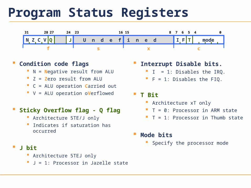
Program Status Registers
Condition code flags N = Negative result from ALU
Z = Zero result from ALU
C = ALU operation Carried out
V = ALU operation oVerflowed
Sticky Overflow flag - Q flag Architecture 5TE/J only
Indicates if saturation has occurred
J bit Architecture 5TEJ only
J = 1: Processor in Jazelle state
Interrupt Disable bits. I = 1: Disables the IRQ.
F = 1: Disables the FIQ.
T Bit Architecture xT only
T = 0: Processor in ARM state
T = 1: Processor in Thumb state
Mode bits Specify the processor mode
2731
N Z C V Q
28 67
I F T mode
1623
815
5 4 024
f s x c
U n d e f i n e dJ

7039v12
When the processor is executing in ARM state: All instructions are 32 bits wide
All instructions must be word aligned
Therefore the pc value is stored in bits [31:2] with bits [1:0] undefined (as instruction cannot be halfword or byte aligned)
When the processor is executing in Thumb state: All instructions are 16 bits wide
All instructions must be halfword aligned
Therefore the pc value is stored in bits [31:1] with bit [0] undefined (as instruction cannot be byte aligned)
When the processor is executing in Jazelle state: All instructions are 8 bits wide
Processor performs a word access to read 4 instructions at once
Program Counter (r15)

88
ARM instructions can be made to execute conditionally by postfixing them with the appropriate condition code field.
This improves code density and performance by reducing the number of forward branch instructions.
CMP r3,#0 CMP r3,#0 BEQ skip ADDNE r0,r1,r2 ADD r0,r1,r2skip
By default, data processing instructions do not affect the condition code flags but the flags can be optionally set by using “S”. CMP does not need “S”.
loop … SUBS r1,r1,#1 BNE loop if Z flag clear then branch
decrement r1 and set flags
Conditional Execution and Flags
99
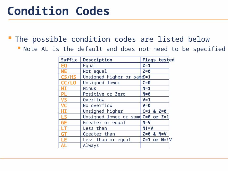
Condition Codes
Not equalUnsigned higher or sameUnsigned lowerMinus
Equal
OverflowNo overflowUnsigned higherUnsigned lower or same
Positive or Zero
Less thanGreater thanLess than or equalAlways
Greater or equal
EQNECS/HSCC/LO
PLVS
HILSGELTGTLEAL
MI
VC
Suffix Description
Z=0C=1C=0
Z=1Flags tested
N=1N=0V=1V=0C=1 & Z=0C=0 or Z=1N=VN!=VZ=0 & N=VZ=1 or N=!V
The possible condition codes are listed below Note AL is the default and does not need to be specified
1010
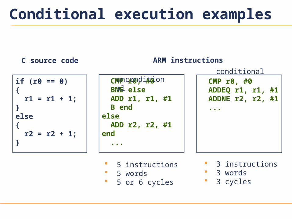
Conditional execution examples
if (r0 == 0){ r1 = r1 + 1;}else{ r2 = r2 + 1;}
C source code
5 instructions 5 words 5 or 6 cycles
3 instructions 3 words 3 cycles
CMP r0, #0 BNE else ADD r1, r1, #1 B endelse ADD r2, r2, #1end ...
ARM instructions
unconditional
CMP r0, #0 ADDEQ r1, r1, #1 ADDNE r2, r2, #1 ...
conditional
1111
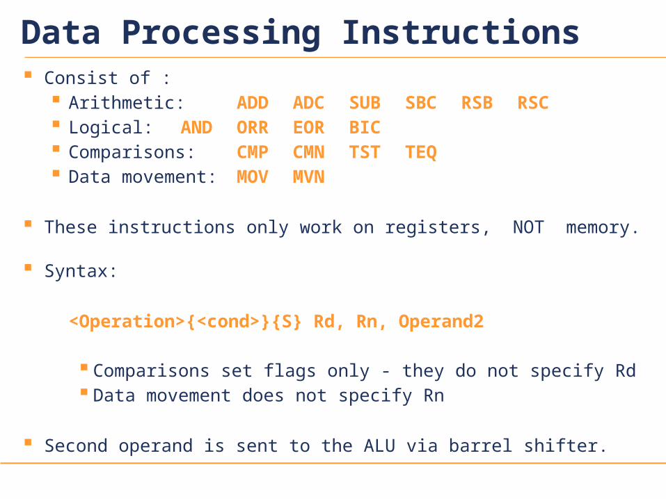
Data Processing Instructions Consist of :
Arithmetic: ADD ADC SUB SBC RSB RSC Logical: AND ORR EOR BIC Comparisons: CMP CMN TST TEQ Data movement: MOV MVN
These instructions only work on registers, NOT memory.
Syntax:
<Operation>{<cond>}{S} Rd, Rn, Operand2
Comparisons set flags only - they do not specify Rd Data movement does not specify Rn
Second operand is sent to the ALU via barrel shifter.

1212
Register, optionally with shift operation
Shift value can be either be:
5 bit unsigned integer
Specified in bottom byte of another register.
Used for multiplication by constant
Immediate value
8 bit number, with a range of 0-255.
Rotated right through even number of positions
Allows increased range of 32-bit constants to be loaded directly into registers
Result
Operand 1
BarrelShifter
Operand 2
ALU
Using a Barrel Shifter:The 2nd Operand

1313
Data Processing Exercise
1. How would you load the two’s complement representation of -1 into Register 3 using one instruction?
2. Implement an ABS (absolute value) function for a registered value using only two instructions.
3. Multiply a number by 35, guaranteeing that it executes in 2 core clock cycles.

1414
Data Processing Solutions
1. MOVN r6, #0
2. MOVS r7,r7 ; set the flags
RSBMI r7,r7,#0 ; if neg, r7=0-r7
3. ADD r9,r8,r8,LSL #2 ; r9=r8*5
RSB r10,r9,r9,LSL #3 ; r10=r9*7

1515
No ARM instruction can contain a 32 bit immediate constant All ARM instructions are fixed as 32 bits long
The data processing instruction format has 12 bits available for operand2
4 bit rotate value (0-15) is multiplied by two to give range 0-30 in steps of 2
Rule to remember is
“8-bits rotated right by an even number of bit positions”
0711 8
immed_8
ShifterROR
rot
x2
Quick Quiz: 0xe3a004ffMOV r0, #???
Immediate constants

1616
To allow larger constants to be loaded, the assembler offers a pseudo-instruction: LDR rd, =const
This will either: Produce a MOV or MVN instruction to generate the value (if possible).
or Generate a LDR instruction with a PC-relative address to read the
constant from a literal pool (Constant data area embedded in the code).
For example LDR r0,=0xFF => MOV r0,#0xFF LDR r0,=0x55555555 => LDR r0,[PC,#Imm12]
……DCD 0x55555555
This is the recommended way of loading constants into a register
Loading 32 bit constants
1717
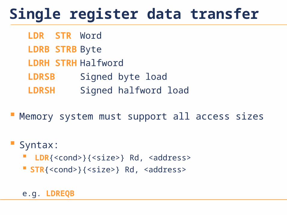
Single register data transfer LDR STR Word
LDRB STRB Byte
LDRH STRH Halfword
LDRSB Signed byte load
LDRSH Signed halfword load
Memory system must support all access sizes
Syntax: LDR{<cond>}{<size>} Rd, <address>
STR{<cond>}{<size>} Rd, <address>
e.g. LDREQB

1818
Address accessed
Address accessed by LDR/STR is specified by a base register with an offset
For word and unsigned byte accesses, offset can be:
An unsigned 12-bit immediate value (i.e. 0 - 4095 bytes)LDR r0, [r1, #8]
A register, optionally shifted by an immediate valueLDR r0, [r1, r2]LDR r0, [r1, r2, LSL#2]
This can be either added or subtracted from the base register:LDR r0, [r1, #-8]LDR r0, [r1, -r2, LSL#2]
For halfword and signed halfword / byte, offset can be:
An unsigned 8 bit immediate value (i.e. 0 - 255 bytes)
A register (unshifted)
Choice of pre-indexed or post-indexed addressing
Choice of whether to update the base pointer (pre-indexed only)
LDR r0, [r1, #-8]!

1919
Load/Store Exercise
Assume an array of 25 words. A compiler associates y with r1. Assume that the base address for the array is located in r2. Translate this C statement/assignment using just three instructions:
array[10] = array[5] + y;

2020
Load/Store Exercise Solution
array[10] = array[5] + y;
LDR r3, [r2, #5] ; r3 = array[5]
ADD r3, r3, r1 ; r3 = array[5] + y
STR r3, [r2, #10] ; array[5] + y = array[10]
2121
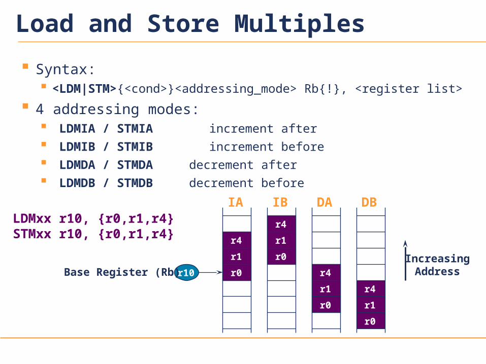
Load and Store Multiples
Syntax: <LDM|STM>{<cond>}<addressing_mode> Rb{!}, <register list>
4 addressing modes: LDMIA / STMIA increment after
LDMIB / STMIB increment before
LDMDA / STMDA decrement after
LDMDB / STMDB decrement beforeIA
r1 IncreasingAddress
r4
r0
r1
r4
r0
r1
r4
r0 r1
r4
r0
r10
IB DA DBLDMxx r10, {r0,r1,r4}STMxx r10, {r0,r1,r4}
Base Register (Rb)

2222
There are 2 classes of multiply - producing 32-bit and 64-bit results
32-bit versions on an ARM7TDMI will execute in 2 - 5 cycles
MUL r0, r1, r2 ; r0 = r1 * r2 MLA r0, r1, r2, r3 ; r0 = (r1 * r2) + r3
64-bit multiply instructions offer both signed and unsigned versions
For these instruction there are 2 destination registers
[U|S]MULL r4, r5, r2, r3 ; r5:r4 = r2 * r3 [U|S]MLAL r4, r5, r2, r3 ; r5:r4 = (r2 * r3) + r5:r4
Most ARM cores do not offer integer divide instructions
Division operations will be performed by C library routines or inline shifts
Multiply and Divide

2323
Branch : B{<cond>} label Branch with Link : BL{<cond>} subroutine_label
The processor core shifts the offset field left by 2 positions, sign-extends it and adds it to the PC
± 32 Mbyte range
How to perform longer branches?
2831 24 0
Cond 1 0 1 L Offset
Condition field
Link bit 0 = Branch1 = Branch with link
232527
Branch instructions

2424
Register Usage
r8r9/sbr10/slr11
r12
r13/spr14/lrr15/pc
r0r1r2r3
r4r5r6r7Register variables
Must be preserved
Arguments into functionResult(s) from function
otherwise corruptible(Additional parameters
passed on stack)
Scratch register(corruptible)
Stack PointerLink Register
Program Counter
The compiler has a set of rules known as a Procedure Call Standard that determine how to pass parameters to a function (see AAPCS)
CPSR flags may be corrupted by function call.Assembler code which links with compiled code must follow the AAPCS at external interfaces
The AAPCS is part of the new ABI for the ARM Architecture
Register
- Stack base- Stack limit if software stack checking selected
- R14 can be used as a temporary once value stacked- SP should always be 8-byte (2 word) aligned

25039v12
ARM Branches and Subroutines B <label>
PC relative. ±32 Mbyte range.
BL <subroutine> Stores return address in LR
Returning implemented by restoring the PC from LR
For non-leaf functions, LR will have to be stacked
STMFD sp!,{regs,lr}
:
BL func2
:
LDMFD sp!,{regs,pc}
func1 func2
:
:
BL func1
:
:
:
:
:
:
:
MOV pc, lr

2626
PSR access
MRS and MSR allow contents of CPSR / SPSR to be transferred to / from a general purpose register or take an immediate value
MSR allows the whole status register, or just parts of it to be updated
Interrupts can be enable/disabled and modes changed, by writing to the CPSR
Typically a read/modify/write strategy should be used:
MRS r0,CPSR ; read CPSR into r0
BIC r0,r0,#0x80 ; clear bit 7 to enable IRQ
MSR CPSR_c,r0 ; write modified value to ‘c’ byte only
In User Mode, all bits can be read but only the condition flags (_f) can be modified
f s x c
2731
N Z C V Q
28 67
I F T mode
1623
15
5 4 024
J
10 89 19
GE[3:0] E A IT cond_abcde

2727
Agenda
Introduction to ARM Ltd
Fundamentals, Programmer’s Model, and Instructions
Core Family Pipelines
AMBA

2828
Pipeline changes for ARM9TDMI
InstructionFetch
Shift + ALU MemoryAccess
RegWriteReg
ReadReg
Decode
FETCH DECODE EXECUTE MEMORY WRITE
ARM9TDMI
ARM or ThumbInst Decode
Reg Select
RegRead Shift ALU Reg
WriteThumbARMdecompress
ARM decodeInstruction
Fetch
FETCH DECODE EXECUTE
ARM7TDMI

2929
ARM10 vs. ARM11 Pipelines
ARM11
Fetch1
Fetch2
Decode Issue
Shift ALU Saturate
Writeback
MAC1
MAC2
MAC3
AddressData
Cache1
DataCache
2
Shift + ALUMemoryAccess Reg
Write
FETCH DECODE EXECUTE MEMORY WRITE
Reg Read
Multiply
BranchPrediction
InstructionFetch
ISSUE
ARM or Thumb
InstructionDecode Multiply
Add
ARM10

3030
Agenda
Introduction to ARM Ltd
Fundamentals, Programmer’s Model, and Instructions
Core Family Pipelines
AMBA

31039v12
Example ARM-based System
16 bit RAM
8 bit ROM
32 bit RAM
ARMCore
I/OPeripherals
InterruptController
nFIQnIRQ

32039v12
High PerformanceARM processor
High-bandwidthon-chip RAM
HighBandwidth
ExternalMemoryInterface
DMABus Master
APBBridge
Timer
Keypad
UART
PIO
AHB
APB
High PerformancePipelinedBurst SupportMultiple Bus Masters
Low PowerNon-pipelinedSimple Interface
An Example AMBA System

33039v12
HWDATA
Arbiter
Decoder
Master#1
Master#3
Master#2
Slave#1
Slave#4
Slave#3
Slave#2
Address/Control
Write Data
Read Data
HADDR
HWDATA
HRDATA
HADDR
HRDATA
AHB Structure


