VBAT
GDRV1
ISNS1
ISP1ISN1
VOUT1PWMO1OVFB1
PWIN1
VIN
COMP1
AG
ND
VCC
PGND1
RT
ICTRL1
DIAG1D1
CO1
RSNS1
Q1
ROV1
ROV2
CIN1
RLIM1
L2
D3
D5
Cs1
Q3
Q6
Q5
Q4
Q9
Q8
Q7
Q11
Q10
CHANNEL 1
TPS92601-Q1
L1
Q12
Copyright © 2017, Texas Instruments Incorporated
1TIDUCU6–June 2017Submit Documentation Feedback
Copyright © 2017, Texas Instruments Incorporated
Automotive LED Front Lamp With Sequential Turn Animation ReferenceDesign
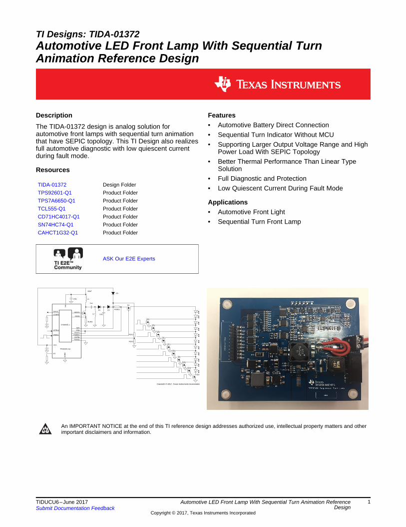
TI Designs: TIDA-01372Automotive LED Front Lamp With Sequential TurnAnimation Reference Design
DescriptionThe TIDA-01372 design is analog solution forautomotive front lamps with sequential turn animationthat have SEPIC topology. This TI Design also realizesfull automotive diagnostic with low quiescent currentduring fault mode.
Resources
TIDA-01372 Design FolderTPS92601-Q1 Product FolderTPS7A6650-Q1 Product FolderTCL555-Q1 Product FolderCD71HC4017-Q1 Product FolderSN74HC74-Q1 Product FolderCAHCT1G32-Q1 Product Folder
ASK Our E2E Experts
Features• Automotive Battery Direct Connection• Sequential Turn Indicator Without MCU• Supporting Larger Output Voltage Range and High
Power Load With SEPIC Topology• Better Thermal Performance Than Linear Type
Solution• Full Diagnostic and Protection• Low Quiescent Current During Fault Mode
Applications• Automotive Front Light• Sequential Turn Front Lamp
An IMPORTANT NOTICE at the end of this TI reference design addresses authorized use, intellectual property matters and otherimportant disclaimers and information.

System Description www.ti.com
2 TIDUCU6–June 2017Submit Documentation Feedback
Copyright © 2017, Texas Instruments Incorporated
Automotive LED Front Lamp With Sequential Turn Animation ReferenceDesign
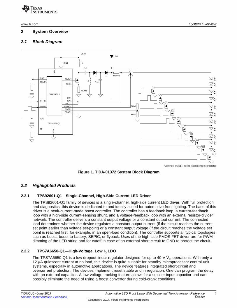
1 System DescriptionThe TIDA-01372 TI Design is for an automotive front light with a sequential turn indicator with fulldiagnostics. In this TI Design, linear light-emitting diode (LED) drivers (TPS92601-Q1) are used to drivethe LEDs with constant current with SEPIC topology. The TPS7A6650-Q1 works as the power supply ofthe TLC555-Q1, CD74HC4017-Q1, SN74HC74-Q1, and CAHCT1G32-Q1. The EN pin is controlled by thecarry in and fault signal, then the system fault will turn off the LDO and decrease system fault modeconsumption current. The TPS7A6650-Q1 PG pin controls TLC555-Q1 and SN74HC74-Q1 reset pin tomake sure these two devices reset out during every power down. In this TI Design, the TLC555-Q1 isused to generate a PWM as the clock of the CD74HC4017-Q1 and decide the delay time between theLED string turnon. The TLC555-Q1 also offers the clock for the SN74HC74 to generate the Carry outsignal. In the design, the CD74HC4017-Q1 generates the 9 PWM on the signal to control thecorresponding MOSFET turnon and turnoff in sequence. Then the SN74HC74 generates the turnon signalof the whole LED string.
1.1 Key System Specifications
Table 1. Key System Specifications
PARAMETER SPECIFICATIONSInput voltage range 6 to 16 VOutput current 500 mA/ChDelay time for string on during sequential turn indicator 30 msLED number 11 sLED type LW-W5SG, OSRAMFault mode current < 2 mA
VBAT
GDRV1
ISNS1
ISP1ISN1
VOUT1PWMO1OVFB1
PWIN1
VIN
COMP1
AG
ND
VCC
PGND1
RT
ICTRL1
DIAG1D1
CO1
RSNS1
Q1
ROV1
ROV2
CIN1
RLIM1
L2
D3
D5
Cs1
Q3
Q6
Q5
Q4
Q9
Q8
Q7
Q11
Q10
CHANNEL 1
TPS92601-Q1
L1
Q12
Copyright © 2017, Texas Instruments Incorporated
www.ti.com System Overview
3TIDUCU6–June 2017Submit Documentation Feedback
Copyright © 2017, Texas Instruments Incorporated
Automotive LED Front Lamp With Sequential Turn Animation ReferenceDesign
2 System Overview
2.1 Block Diagram
Figure 1. TIDA-01372 System Block Diagram
2.2 Highlighted Products
2.2.1 TPS92601-Q1—Single-Channel, High-Side Current LED DriverThe TPS92601-Q1 family of devices is a single-channel, high-side current LED driver. With full protectionand diagnostics, this device is dedicated to and ideally suited for automotive front lighting. The base of thisdriver is a peak-current-mode boost controller. The controller has a feedback loop, a current-feedbackloop with a high-side current-sensing shunt, and a voltage-feedback loop with an external resistor-dividernetwork. The controller delivers a constant output voltage or a constant output current. The connectedload determines whether the device regulates a constant output current (if the circuit reaches the currentset point earlier than voltage set-point) or a constant output voltage (if the circuit reaches the voltage setpoint is reached first, for example, in an open-load condition). The controller supports all typical topologiessuch as boost, boost-to-battery, SEPIC, or flyback. Uses of the high-side PMOS FET driver are for PWMdimming of the LED string and for cutoff in case of an external short circuit to GND to protect the circuit.
2.2.2 TPS7A6650-Q1—High-Voltage, Low IQ LDOThe TPS7A6650-Q1 is a low dropout linear regulator designed for up to 40-V VIN operations. With only a12-μA quiescent current at no load, this device is quite suitable for standby microprocessor control-unitsystems, especially in automotive applications. The device features integrated short-circuit andovercurrent protection. The devices implement reset stable and in regulation. One can program the delaywith an external capacitor. A low-voltage tracking feature allows for a smaller input capacitor and canpossibly eliminate the need of using a boost converter during cold-crank conditions.
System Overview www.ti.com
4 TIDUCU6–June 2017Submit Documentation Feedback
Copyright © 2017, Texas Instruments Incorporated
Automotive LED Front Lamp With Sequential Turn Animation ReferenceDesign
2.2.3 TLC555-Q1—Timer to Generate PWM Input for High DriverThe TLC555-Q1 is a monolithic timing circuit, which has been fabricated using the TI LinCMOS™technology process. The timer is fully compatible with complementary metal-oxide semiconductor(CMOS), transistor-transistor logic (TTL), and MOS logic and operates at frequencies up to 2 MHz. Thisdevice uses smaller timing capacitors than those used by the NE555 because of its high input impedance.As a result, more accurate time delays and oscillations are possible. Power consumption is low across thefull range of power-supply voltage.
2.2.4 CD74HC4017-Q1—Automotive Decade Counter and Divider With 10 Decode OutputsThe CD74HC4017 is a high-speed silicon gate CMOS five-stage Johnson counter with 10 decodedoutputs. Each of the decoded outputs is normally low and sequentially goes high on the low- to high-transition clock period of the 10 clock period cycle. The device can drive up to 10 low-power Schottkyequivalent loads.
2.2.5 SN74HC74-Q1—Dual D-Type Positive-Edge-Triggered Flip-Flop With Clear and PresetThe SN74HC74 device contains two independent D-type positive-edge-triggered flip-flops. A low level atthe preset (PRE) or clear (CLR) inputs sets or resets the outputs, regardless of the levels of the otherinputs. When PRE and CLR are inactive (high), data at the data (D) input meeting the setup timerequirements are transferred to the outputs on the positive-going edge of the clock (CLK) pulse. Clocktriggering occurs at a voltage level and is not directly related to the rise time of CLK.
2.2.6 CAHCT1G32-Q1—Single Two-Input Positive-OR GateThe SN74AHCT1G32 is a single two-input positive-OR gate. The device performs the Boolean functionY = A + B or Y = A × B in positive logic.
2.3 Design ConsiderationsThe TIDA-01372 design uses a 1-pcs TPS92601-Q1 to drive one white LED string and the current string isset at 500 mA. When input V-BAT connects to battery, the LED strings will turn on by sequence with anadjustable delay time to implement sequential turn animation. The TLC555-Q1 is used to generate a PWMas a clock of the CD74HC4017-Q1 and decide the delay time between LED string turnon. TheCD74HC4017 generates the nine PWM pluses to control corresponding LED turnon in sequence.
(DNP)C30
(DNP)
R44
0.1uFC31
10uFC32
GND
2.2uFC16GND
ICTRL11
COMP12
OVFB1 3
RT4
DIAG15
GND6
PWMIN17
VIN8
NC9
NC10
NC11
NC12
VCC13
GDRV114
ISNS115
PGND116
ISP117
ISN1 18
VOUT119
PWMO120
PAD21
U7
TPS92601AQPWPRQ1
GND
VCC
GND
GNDGND
GND
191kR59
40.2kR61
0.22uFC34
VCC
10µFC14
OPEN
C15
NCC28
10k
R45GND
GND
VIN
VIN
ISP
ISN
OVFB
OVFB
ISN
ISP
Int_Fault
0.22µFC23
D3
PMEG10010ELRX
Q9
ZXMP10A16KTC0
R56
ENB_DRV
0.57VD6
PMEG2005EH
10R47
VOUT
3.3V
D71SMB5913BT3G
0.3
R40
C18 C19C17NCC20
4.7µFC21
0.1µFC22
4.7µH
L2
4.7µFC24
D4MBRA340T3G
NCC25
NCC27
NCC29
L3
1 2
3 4
10µH
L1
MSD1514-103MEB
1
2
J2
039544-3002
0
R53
0R54
0
R49
12
34
L4
51R55
GNDLED+
392k
R52VCC
GND
Reserved for the EMI test
Reserved for the EMI test
172kR42
1
4
3
D5
30WQ06FNPBF10µFC26
0.015
R50
100V
MN_POWER?SUD40N10-25
220pFC33
Copyright © 2017, Texas Instruments Incorporated
www.ti.com System Overview
5TIDUCU6–June 2017Submit Documentation Feedback
Copyright © 2017, Texas Instruments Incorporated
Automotive LED Front Lamp With Sequential Turn Animation ReferenceDesign
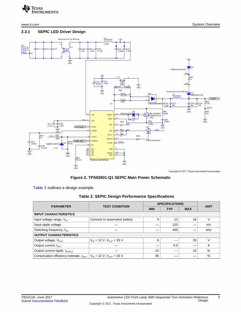
2.3.1 SEPIC LED Driver Design
Figure 2. TPS92601-Q1 SEPIC Main Power Schematic
Table 2 outlines a design example.
Table 2. SEPIC Design Performance Specifications
PARAMETER TEST CONDITIONSPECIFICATIONS
UNITMIN TYP MAX
INPUT CHARACTERISTICSInput voltage range, VIN Connect to automotive battery 6 12 16 VInput ripple voltage — — 120 — mVSwitching frequency, fSW — — 400 — kHzOUTPUT CHARACTERISTICSOutput voltage, VOUT VIN = 12 V, VOUT = 33 V 6 — 33 VOutput current, IOUT — — 0.5 — AOutput current ripple, IRIPPLE — –10 — 10 %Conservative efficiency estimate, ηEST VIN = 12 V, VOUT = 33 V 85 — — %

LED FDMAX
LED MIN FD
V V 33 V 0.5 VD 84.8%
V V V 33 V 6 V 0.5 V
+ +» = =
+ + + +
LED FDMIN
LED MAX FD
V V 33 V 0.5 VD 67.7%
V V V 33 V 16 V 0.5 V
+ +» = =
+ + + +
( )39.6 2.2R4217
R45 2.2
-= =
( )OVPT VFB
VFB
V VR42
R45 V
-=
150 mVR6 0.3
0.5 A= = W
SPSN_DIFFSENSE
SETTING
VR
I=
( )( )RT
OSC
12.5 MHz 1 kR k
f MHz
´ WW =
System Overview www.ti.com
6 TIDUCU6–June 2017Submit Documentation Feedback
Copyright © 2017, Texas Instruments Incorporated
Automotive LED Front Lamp With Sequential Turn Animation ReferenceDesign
2.3.1.1 Detailed Design ProcedureTo begin the design process, one must decide on the following:• Input voltage range• Output current• Output voltage• Input ripple voltage• Output ripple current
2.3.1.2 Switching FrequencyIn this TI Design, the frequency is 400 kHz. The RT pin resistor sets the switching frequency of theTPS92601-Q1 device. Use Equation 1 to calculate the required value for R51. The calculated value is31.25 kΩ. Use the nearest standard value of 31.2 kΩ.
(1)
2.3.1.3 Max Output Current Set PointThe output constant of the TPS92601 is adjustable by using the external current shunt resistor. In theapplication circuit of Figure 2, R40 is current shunt resistor, the max output current is given by Equation 2.
(2)
2.3.1.4 Output Overvoltage Protection Set PointThe output overvoltage protection threshold of the TPS92601 is externally adjustable using a resistordivider network. The relationship of the overvoltage protection threshold (VOVPT) to the resistor divider isgiven by Equation 3.
(3)
The load are 11 pcs white LED, then the LED forward voltage is about 33 V in max forward voltage. If oneneeds a 20% margin for the overvoltage protection, the VOVPT will be: VOVPT = 33 × 1.2 = 39.6 V.
So, . Select R45 = 10K, then R42 = 170 kΩ. Use the nearly standard value of 172 kΩ.
2.3.1.5 Duty Cycle EstimationFor further calculations, the minimum and maximum duty cycles are first estimated in continuousconduction mode (CCM). Estimate the duty cycle of the main switching MOSFET using Equation 4 andEquation 5.
(4)
(5)
where D is the duty cycle
Using and estimated forward drop of 0.5 V for a Schottky rectifier diode, the approximate duty cycle is67.7% (minimum) to 84.8% (maximum) in max power out.

L _ peakI 3.5534 0.818 4.3714 A= + =
RIPPLE RIPPLEL _ peak La _ peak Lb _ peak IN_ min OUT
I II I I I I
2 2
æ ö æ ö= + = + + +ç ÷ ç ÷ç ÷ ç ÷
è ø è ø
RIPPLELb _ peak OUT
I 0.636I I 0.5 0.818 A
2 2= + = + =
RIPPLELa _ peak IN_min
I 0.636I I 3.2354 3.5534 A
2 2= + = + =
IN
RIPPLE MAX
SW
V 1 16 V 1I D 0.848 1.636 A
2 L f 20 H 400 kHz» ´ ´ = ´ ´ =
´ m
IN
RIPPLE MIN
SW
V 1 16 V 1I D 0.677 1.354 A
2 L f 20 H 400 kHz» ´ ´ = ´ ´ =
´ m
Lb _RMS OUTI I 0.5 A» =
OUT OUTLa _RMS
IN_ min
V I 33 0.5I 3.235 A
V 6 0.85
´ ´= = =
´ h ´
IN_ minMIN MAX
Lrip _ max SW
V 1 6 V 1L D 0.848 7.709 H
2 I f 2 0.825 A 400 kHz>> ´ ´ = ´ ´ = m
´ ´
OUT OUTLrip _ max
IN_ min
I V 0.5 33I 0.3 0.3 0.825 A
V 6
´ ´
= ´ = ´ =
www.ti.com System Overview
7TIDUCU6–June 2017Submit Documentation Feedback
Copyright © 2017, Texas Instruments Incorporated
Automotive LED Front Lamp With Sequential Turn Animation ReferenceDesign
2.3.1.6 Inductor SelectionInductors L1 and L2 could be uncoupled, but then they must be twice as large as if they are coupled.Another advantage is that if coupled inductors are used there is very small input current ripple.
The peak-to-peak ripple is limited to 30% of the maximum output current (see Equation 6).
(6)
Because the two windings of a coupled inductor share the ripple current, the inductance value can behalved. The minimum inductor size can be estimated using Equation 7.
(7)
The near higher standard inductor value of 10 µH is selected.
Equation 8 and Equation 9 calculate the RMS current in each winding. Equation 15 and Equation 16 takethese currents and converts them to the ratings IRMS_one and IRMS_both, typically shown on the datasheets ofcoupled inductors. IRMS_one represents only one winding conducting and IRMS_both represents both windingsconducting equally. The ratings are typically given for a 40°C temperature rise.
(8)
(9)
The ripple current is estimated by Equation 10.
(10)
(11)
The worst-case peak-to-peak ripple current occurs at 84.8% duty cycle and is estimated as 0.636 A.
In a coupled inductor, the total peak current is the sum of the peak current in each winding. Equation 14calculates the peak current.
(12)
(13)
(14)

OUT _ ripple
L _ peak
V 0.05 5.5 mVESR 1.26 m
I 4.371 A
´= = = W
OUTOUT
VOUT _ ripple SW
I D 1 0.5 A 0.848 1C 10.14 F
V 0.95 f 110 mV 0.95 400 kHz
´ æ ö´= ´ = ´ = mç ÷´ ´è ø
VOUT _ rippleV 0.05 A 2.2 110 mV= ´ W =
D _ max F OUT _ maxP V I 0.5 0.5 A 0.25 W» ´ = ´ =
D _ peak L _ peakI I 4.371 A= =
D _ avg OUT _ maxI I 0.5 A» =
VOPT IN_ max FDBR _R_min
V V VV 1.25 56.1 V 70 V
0.8
+ +
³ = ´ =
( )2 2 2L La _RMS Lb _RMSP I I DCR (3.273 ) 15 161 mW= + ´ = ´ =
2 2 2RMS _ one
RMS _ both
I 3.235 0.5I 2.315 A
2 2
+= » =
2 2 2 2RMS _ one La _RMS Lb _RMSI I I 3.235 0.5 3.273 A= + » + =
System Overview www.ti.com
8 TIDUCU6–June 2017Submit Documentation Feedback
Copyright © 2017, Texas Instruments Incorporated
Automotive LED Front Lamp With Sequential Turn Animation ReferenceDesign
For this TI Design, the peak current is estimated to be 4.3714 A. It is recommended that the saturationcurrent of the inductor be 20% higher than the peak current or greater than the peak current limit of the IC.This leaves a margin for transient conditions when the peak inductor current may increase above thesteady state value. Using the peak current limit of the IC is the most conservative criteria and ensures theinductor does not become saturated during an overcurrent fault condition. The TIDA-01372 design usesthe 5.245-A typical current limit for the minimum saturation current rating.
(15)
(16)
In this TI Design, select the MSD1514-103MEB.
(17)
2.3.1.7 Rectifier Diode SelectionSimilar to a boost converter, the average current through the diode is equal to the output current. Therectifying diode must be chosen to handle the output current and voltage at the switching node. At least a25% margin is recommended for the diode’s average current rating. A conservative design uses themaximum output current with VIN_max with the typical current limit to choose the current rating. A low-forward voltage drop Schottky diode is used as a rectifier diode to reduce its power dissipation andimprove efficiency. Using a 80% derating on VOUT for ringing on the switch node, the rectifier diodeminimum reverse breakdown voltage is given by Equation 18.
(18)
The diode must have reverse breakdown voltage greater than 70 V. The rectifier diode peak and averagecurrents are estimated by Equation 19 and Equation 20.
(19)
(20)
For this TI Design, the peak current is 4.371 A.
The power dissipation in the diode is estimated by Equation 21.
(21)
For this TI Design, the maximum power dissipation is estimated as 0.25 W. Reviewing the 70-V Schottkydiodes, the 30WQ10FNPBF, Schottky, 100-V, 3.5-A DPAK is selected. This diode has a forward voltagedrop of 0.35 V at 1 A, so the conduction power dissipation is less than 170 mW and less than half its ratedpower dissipation.
2.3.1.8 Output Capacitor SelectionAssume a maximum LED current ripple of 0.1 × ILED. Also, assume that the dynamic impedance of thechosen LED is 0.2 Ω (2.2 Ω in total for the 11-LED string). The total output voltage ripple is then calculatedas follows:
(22)
Assuming a ripple contribution of 95% from bulk capacitance, the output capacitor is calculated as follows:
(23)
(24)
Select one 10-μF capacitors and ensure that the chosen capacitors meet the minimum bulk capacitancerequirement at the operating voltage.

Q _ peak La _ peak Lb _ peakI I I 4.371 A= + =
FET DISS _ total L D RSNS IN_ max VDDP P P P P V Ic
< - - - - ´
DISS _ total OUT
1 1P P 1 33 V 0.5 A 1 2.912 W
0.85
æ ö æ ö» ´ - = ´ ´ - =ç ÷ ç ÷h è øè ø
( )BD _MOS _ min VOPT IN_ maxV V V 1.3 1.3 55.6 V 77.3 V³ ´ ´ = ´ =
ISNSISNS
L _ peak
V 100 mVR 17.6 m
1.3 I 1.3 4.371 A
cc = = = W
´ ´
IN_RIPPLEESR
IN_DC
V 60 mVR 18.5 m
I 3.235 A< = = W
RIPPLE _ VinminIN
IN_RIPPLE SW
I 0.636 AC 6.62 F
4 V f 4 60 mV 400 kHz> = = m
´ ´ ´ ´
( ) ( )MAX
CP _RMS IN_DCMAX
1 D 1 0.848I I 3.235 1.370 A
D 0.848
- -= ´ = ´ =
OUT MAX
IN_ max SW
I D 0.5 A 0.848Cp 1.325 F
0.05 V f 0.05 16 V 400 kHz
´ ´³ = = m
´ ´ ´ ´
www.ti.com System Overview
9TIDUCU6–June 2017Submit Documentation Feedback
Copyright © 2017, Texas Instruments Incorporated
Automotive LED Front Lamp With Sequential Turn Animation ReferenceDesign
2.3.1.9 AC Capacitor (C16)It is recommended to choose the AC capacitor (Cp) so the ripple voltage ΔVCP is no more than 5% of themaximum VCPDC equal to VIN_max. Equation 25 calculates the minimum capacitance.
(25)
The minimum capacitance is calculated to be 1.325 μF, and due to derating, the next highest standardvalue of 2.2 μF is used. This capacitor must be rated for the maximum input voltage and capacitancederating due to DC bias should be considered. The capacitor must also be rated for the RMS current(ICP_RMS). This is calculated as 1.370 A using Equation 26. The capacitor selected is a 2.2-μF, 63-V X7R1206 ceramic capacitor.
(26)
2.3.1.10 Input Capacitor SelectionAssume that a maximum of 120 mV of the input ripple can be tolerated (2% of VINMIN). Also assume that50% of this input ripple comes from the bulk capacitance. Based on the stated design specifications, theinput capacitor value is calculated using Equation 27 and Equation 28:
(27)
(28)
For this TI Design, to meet a maximum input ripple of 120 mV, a minimum 10-µF input capacitor with anESR of less than 18.5 mΩ is needed. A 2-pcs, 4.7-µF X7R ceramic capacitor is selected.
2.3.1.11 Current Sense and Current LimitThe maximum allowable current sense resistor value is limited by the inductor peak current. This limitationis given by Equation 29.
(29)
A 15-mΩ resistor is selected.
2.3.1.12 Switching MOSFET SelectionThe TPS92601-Q1 drives a ground referenced N-channel FET. The voltage at SW is the sum of VOUT andVIN plus 30% as a margin.
(30)
An N-channel FET with a breakdown voltage of 100 V is selected.
The RDS(on) and gate charge are estimated based on the desired efficiency target.
(31)
For a target of 85% efficiency with a 16-V input voltage at 1 A, the maximum power dissipation is limitedto 2.912 W. The main power dissipating devices are the MOSFET, inductor, diode, current sense resistor,and the integrated circuit, the TPS92601-Q1 device.
(32)
(33)

GND 1TRIG2
OUT 3
RESET4
CONT5
THRES6
DISCH7
VCC8
U6
TLC555QDRQ1
1µFC10
GND
5V
RESET
GND
0.1uFC12
GND
10kR29
5V
51
12
03
2 4
65
76
3 7
GND 8
89
410
911
TC12
CE13
CP14
MR15
VCC16
U4
CD74HC4017QPWRG4Q1
5V
1µFC8
GND
MR
NCE
CLOCKCTRL1
CTRL2
CTRL3
CTRL4
CTRL5
CTRL6
CTRL7
CTRL8
CTRL9
GND
1.0kR35
GND
9.10kR37
0.47µFC13
45.3kR39
Copyright © 2017, Texas Instruments Incorporated
( ) 9
239 V 4.471 A 9 10 nC 400 kHz
3.031 A 0.02 0.848 0.1558 0.897 1.0528 W0.7 A
-+ ´ ´ ´= ´ W ´ + = + =
( )IN_min OUT Q _ peak GD OSC2FET Q _RMS DS (on) MAX
G
V V I Q fP I R D
I
+ ´ ´ ´= ´ ´ +
( ) ( ) ( ) ( )OUT IN_ min FD OUT FD
Q _RMS OUT 2 2IN_ min
V V V V V 33 6 0.5 33 0.5I I 0.5 3.031 A
V 6
+ + ´ + + + ´ += ´ = ´ =
System Overview www.ti.com
10 TIDUCU6–June 2017Submit Documentation Feedback
Copyright © 2017, Texas Instruments Incorporated
Automotive LED Front Lamp With Sequential Turn Animation ReferenceDesign
(34)
The SUD40N10-25 (RDS(ON) = 20 mΩ and QGD = 9 nC) is selected in this TI Design. The gate drive currentIG of the TPS92601-Q1 is 0.7 A. The estimated power loss is:
(35)
2.3.1.13 Loop CompensationSelect a large compensation capacitor (1 μF) and small compensation resistor (51 Ω) as thecompensation network in the schematic. details in Section 2.12 of the application report Using theTPS55340 as a SEPIC Converter (SLVA516)[6].
2.3.1.14 SEPIC Startup DiodeSince the minimum common-mode voltage of ISP1 and ISN1 of TPS92601-Q1 and there is no currentcharge loop for ISP1 and ISN1 in SEPIC topology, it needs one startup diode D1 from VCC to ISP1 tocharge ISP1 and ISN1 common-mode voltage higher than 4V. In normally application, there are servaluFs cap in the output, so it needs diode to block the ISN1 to VOUT path for charging ISP1 quickly in caseof trigger latch fault. D3 is put in here for this function; it is suggested to select schottky with low forwardvoltage to improve total efficiency.
2.3.2 CLK and Turnon Delay Time DesignTo implement 9 separated PWMs with adjustable shift delay time, CD74HC works for 8-bit parallel-outserial shift registers, in the design, connect pin A and pin B to VCC directly, so the Qx High shift time justdepend on CLK. In this design, the TLC555-Q1 device is used to generate CLK input signal, as Figure 3shows. The following paragraphs describe how to set the CLK period and duty cycle.• tH = 0.693 (R35 + R39)C13
• tH = 0.693 (R39)C13
• period = tH + tL = 0.693 (R35 + 2R39) C13
• CLK = 0.693 × (1 + 2 × 45.3) × 103 × 0.47 × 10–6 = 29.84 ms
So the LEDs will turn on with a 29.84-ms shift delay by sequence.
Figure 3. CLK and PWM Generator Schematic
VIN1
EN2
NC3
CT4
GND5
PG 6
FB/NC 7
VOUT8
PA
D
U2TPS7A6650QDGNRQ1
10k
R6
GND
5V
1
23
Q1
BSR302NL6327HTSA1
GND
RESET
1
23
Q2BSR302NL6327HTSA1
GND
RESET1
33.2k
R20
33.2k
R21
10k
R8
MRCLR
1
D2
CLK3 Q 6
Q 5
PRE4
GND7
VCC14
U1A
SN74HC74PWR
CLR13
D12
CLK11 Q 8
Q 9
PRE10
GND7
VCC14
U1B
SN74HC74PWR
5V
0.1uFC6
GND
1.0k
R2
9.1kR13
0.1uFC4
GND
GND
CLOCK
NCE
RESET
CTRL9
1
2
3
4
5
V+
V-
U3CAHCT1G32QDBVRQ1
NCE
9.1kR28
GNDGND
5V
1µF
C7
GND
CTRL10
1µF
C1
GND
Force_AllON
1.0kR7
Q6
BSR302NL6327HTSA133.2kR27
GND
0
R9Carry_out
1.0kR17
Red
12
D1
GND
CLR
RESET
NC
R10
0
R11
0
R1
0.01µFC5
GND
4.7uC2
GND
0R16
Copyright © 2017, Texas Instruments Incorporated
CLR1
D2
CLK3
Q6
Q 5
PRE4
GND7
VCC14
U5A
SN74HC74QPWR
CLR13
D12
CLK11
Q8
Q 9
PRE10
GND7
VCC14
U5B
0
R36
5V
1.0k
R30
0
R33
0.1uFC11
GND
5V
0
R31
0R38
CTRL1_N
1µFC9
GND
CLR
ENB_DRV
0R32
NC
R34
Copyright © 2017, Texas Instruments Incorporated
www.ti.com System Overview
11TIDUCU6–June 2017Submit Documentation Feedback
Copyright © 2017, Texas Instruments Incorporated
Automotive LED Front Lamp With Sequential Turn Animation ReferenceDesign
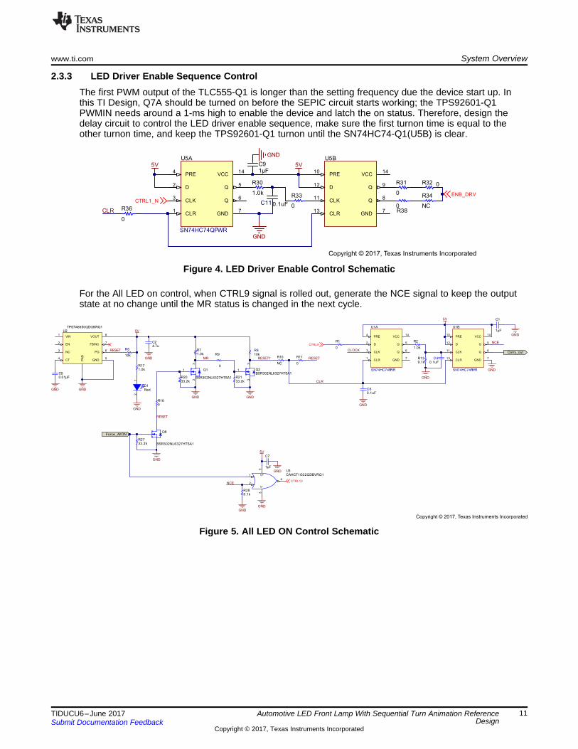
2.3.3 LED Driver Enable Sequence ControlThe first PWM output of the TLC555-Q1 is longer than the setting frequency due the device start up. Inthis TI Design, Q7A should be turned on before the SEPIC circuit starts working; the TPS92601-Q1PWMIN needs around a 1-ms high to enable the device and latch the on status. Therefore, design thedelay circuit to control the LED driver enable sequence, make sure the first turnon time is equal to theother turnon time, and keep the TPS92601-Q1 turnon until the SN74HC74-Q1(U5B) is clear.
Figure 4. LED Driver Enable Control Schematic
For the All LED on control, when CTRL9 signal is rolled out, generate the NCE signal to keep the outputstate at no change until the MR status is changed in the next cycle.
Figure 5. All LED ON Control Schematic
VIN1
EN2
NC3
CT4
GND5
PG 6
FB/NC 7
VOUT8
PA
D
U2TPS7A6650QDGNRQ1
10k
R6
VIN
GND
GND
5V
Carry_in
4.7µFC3
Q3
BSR302NL6327HTSA1
30k
R5
30k
R4
30k
R3
1.0k
R19
5.6V
D2MMSZ4690T1G
GND
Q4
BSR302NL6327HTSA1
50
R23
33.2kR25
GND
Int_FaultQ5
BSR302NL6327HTSA133.2kR26
GND
Ext_Fault
50
R24
1.0kR17
Red
12
D1
GND
RESET
0
R14
0R18
0.01µFC5
GND
91kR22
NCR12
0R15
Copyright © 2017, Texas Instruments Incorporated
System Overview www.ti.com
12 TIDUCU6–June 2017Submit Documentation Feedback
Copyright © 2017, Texas Instruments Incorporated
Automotive LED Front Lamp With Sequential Turn Animation ReferenceDesign
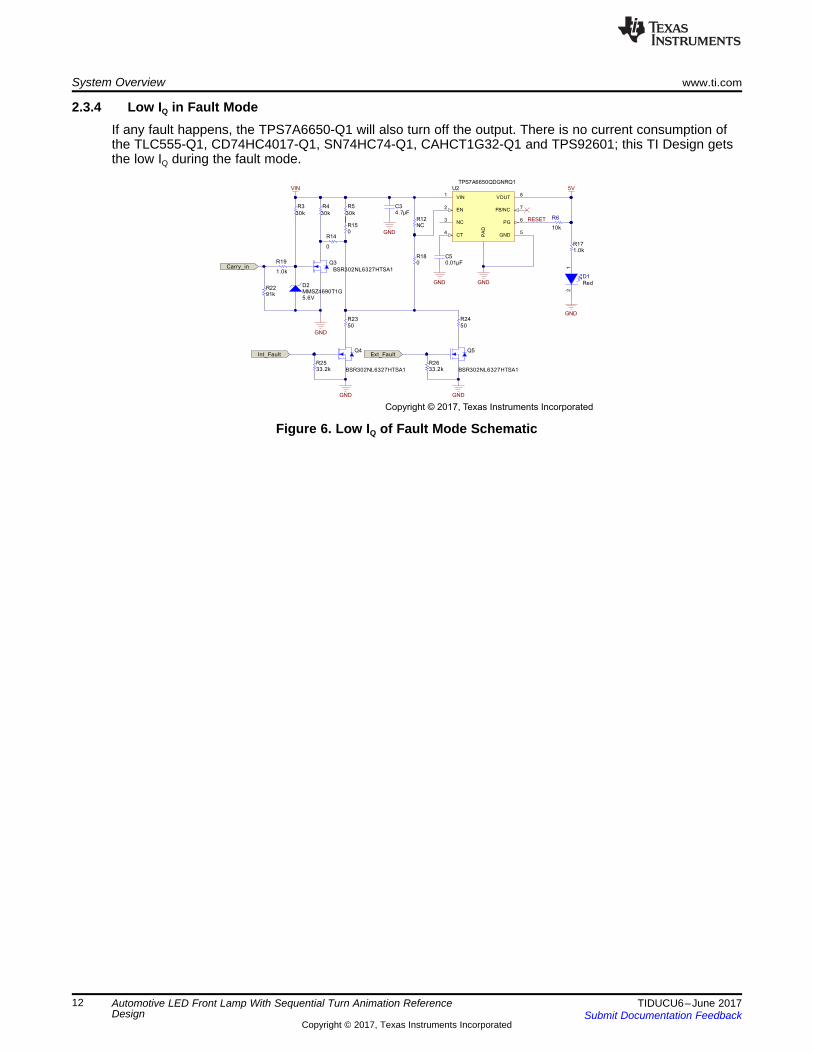
2.3.4 Low IQ in Fault ModeIf any fault happens, the TPS7A6650-Q1 will also turn off the output. There is no current consumption ofthe TLC555-Q1, CD74HC4017-Q1, SN74HC74-Q1, CAHCT1G32-Q1 and TPS92601; this TI Design getsthe low IQ during the fault mode.
Figure 6. Low IQ of Fault Mode Schematic

12V
0V0.5s 1s 1.5s 2s0s 2.5s
Copyright © 2017, Texas Instruments Incorporated
www.ti.com Getting Started Hardware
13TIDUCU6–June 2017Submit Documentation Feedback
Copyright © 2017, Texas Instruments Incorporated
Automotive LED Front Lamp With Sequential Turn Animation ReferenceDesign
3 Getting Started HardwareConnecting a 12-V DC supply through the PWM mode high-side driver with 0.5 s on and 0.5 s off to theonboard input connector (J2) lights up the LED in sequential turn indicator. Connect each LED of the LEDstring to J3 as shown in Figure 8.
Figure 7. Input Voltage of Turn Mode

7,8 Q7A
BUK9K134-100EX
5,6 Q7B
BUK9K134-100EX
7,8 Q10A
BUK9K134-100EX
CTRL1
CTRL2
CTRL3
0
R43
0
R48
0
R57
CTRL4
CTRL5
CTRL6
CTRL7
CTRL8
CTRL9
CTRL10
0
R62
0
R64
0
R66
0
R68
0
R72
0
R70
0
R73
CTRL1_N
5,6 Q10B
BUK9K134-100EX
0
R41
0
R46
0
R51
0
R58
0
R60
0
R63
0
R65
0
R67
0
R69
0
R71
5
4
1
2
3
6
7
8
9
10
11
12
J3
IPL1-112-01-L-S-RA-K
7,8 Q11A
BUK9K134-100EX
5,6 Q11B
BUK9K134-100EX
7,8 Q12A
BUK9K134-100EX
5,6 Q12B
BUK9K134-100EX
7,8 Q13A
BUK9K134-100EX
5,6 Q13B
BUK9K134-100EX
LED+
GND
GND
GND
GND
GND
GND
GND
GND
GND
GND
Copyright © 2017, Texas Instruments Incorporated
Getting Started Hardware www.ti.com
14 TIDUCU6–June 2017Submit Documentation Feedback
Copyright © 2017, Texas Instruments Incorporated
Automotive LED Front Lamp With Sequential Turn Animation ReferenceDesign
Figure 8. LED Connection Schematic
www.ti.com Testing and Results
15TIDUCU6–June 2017Submit Documentation Feedback
Copyright © 2017, Texas Instruments Incorporated
Automotive LED Front Lamp With Sequential Turn Animation ReferenceDesign
4 Testing and Results
4.1 Waveforms
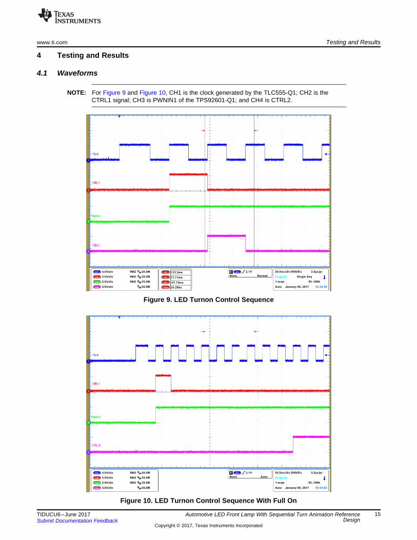
NOTE: For Figure 9 and Figure 10, CH1 is the clock generated by the TLC555-Q1; CH2 is theCTRL1 signal; CH3 is PWNIN1 of the TPS92601-Q1; and CH4 is CTRL2.
Figure 9. LED Turnon Control Sequence
Figure 10. LED Turnon Control Sequence With Full On

Testing and Results www.ti.com
16 TIDUCU6–June 2017Submit Documentation Feedback
Copyright © 2017, Texas Instruments Incorporated
Automotive LED Front Lamp With Sequential Turn Animation ReferenceDesign
NOTE: For Figure 11 and Figure 12, CH1 is the clock generated by the TLC555-Q1; CH2 is theCTRL1 signal; CH3 is VOUT of the SEPIC circuit; and CH4 is the LED string current.
Figure 11. LED String Voltage and Current During Turnon
Figure 12. LED String Voltage and Current After Turnon
www.ti.com Testing and Results
17TIDUCU6–June 2017Submit Documentation Feedback
Copyright © 2017, Texas Instruments Incorporated
Automotive LED Front Lamp With Sequential Turn Animation ReferenceDesign
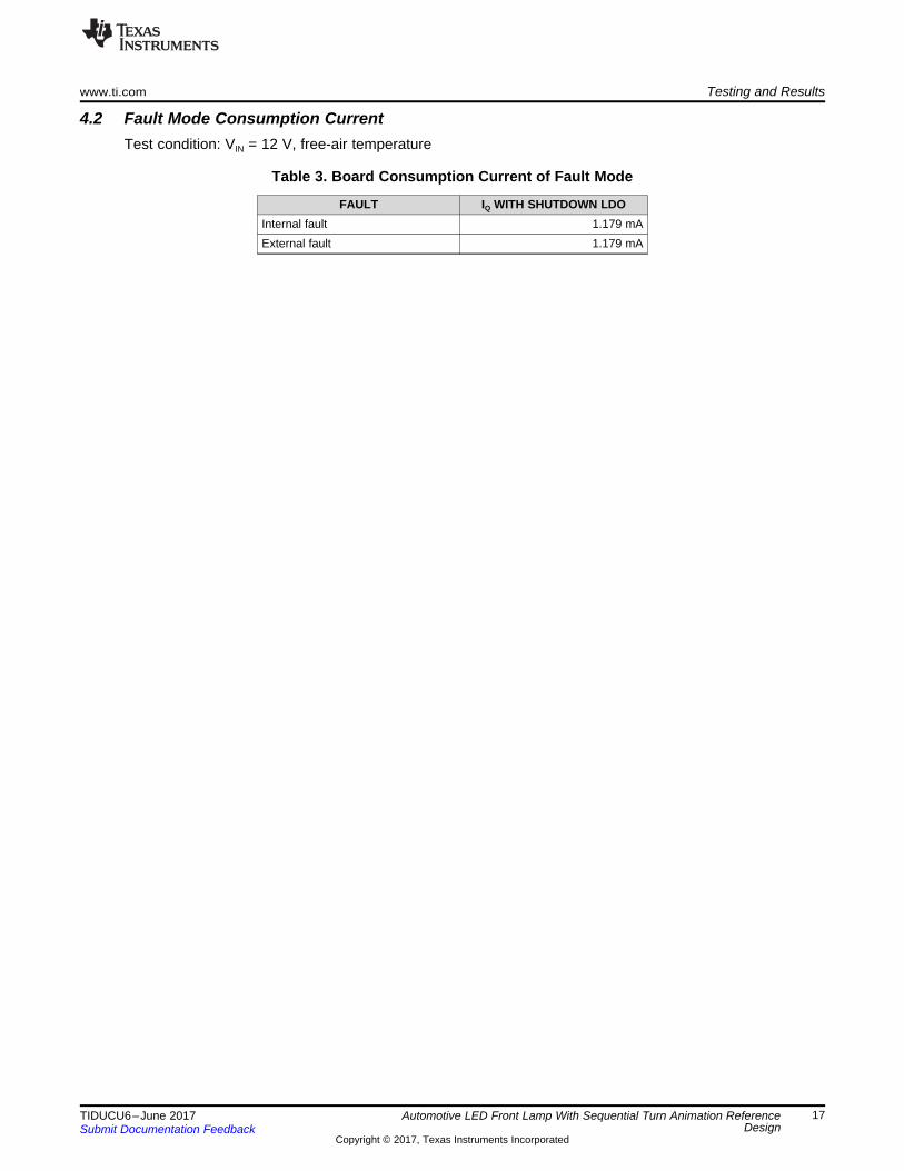
4.2 Fault Mode Consumption CurrentTest condition: VIN = 12 V, free-air temperature
Table 3. Board Consumption Current of Fault Mode
FAULT IQ WITH SHUTDOWN LDOInternal fault 1.179 mAExternal fault 1.179 mA

Design Files www.ti.com
18 TIDUCU6–June 2017Submit Documentation Feedback
Copyright © 2017, Texas Instruments Incorporated
Automotive LED Front Lamp With Sequential Turn Animation ReferenceDesign
5 Design Files
5.1 SchematicsTo download the schematics, see the design files at TIDA-01372.
5.2 Bill of MaterialsTo download the bill of materials (BOM), see the design files at TIDA-01372.
5.3 PCB Layout RecommendationsThe performance of any switching regulator depends as much on the layout of the PCB as the componentselection. Follow these simple guidelines to maximize noise rejection and minimize the generation of EMIwithin the circuit:• Discontinuous currents are the most likely to generate EMI; therefore, take care when routing the
following paths. The main paths for discontinuous current in the TPS92601-Q1 SEPIC regulator arediscontinuous and require careful attention to layout. Keep these loops as small as possible and theconnections between all the components short and thick to minimize parasitic inductance. In particular,make the switch node (where L1, D5, and MN_POWER1 connect) just large enough to connect thecomponents. To minimize excessive heating, place large copper pours adjacent to the short currentpath of the switch node.
• The RT, COMP, ISNS, ICTRL, OVFB, ISP, and ISN pins are all high-impedance inputs, which coupleexternal noise easily. Therefore, minimize the loops containing these nodes whenever possible. Insome applications, the LED or LED array can be far away (several inches or more) from theTPS9260x-Q1 family of devices, or on a separate PCB connected by a wiring harness. When using anoutput capacitor where the LED array is large or separated from the rest of the regulator, place theoutput capacitor close to the LEDs to reduce the effects of parasitic inductance on the ac impedance ofthe capacitor.
• Separate and connect AGND and PGND at the input GND connector.• Separate the control signal as low noise circuit with switching power loop.
5.3.1 Layout PrintsTo download the layer plots, see the design files at TIDA-01372.
5.4 Altium ProjectTo download the Altium project files, see the design files at TIDA-01372.
5.5 Gerber FilesTo download the Gerber files, see the design files at TIDA-01372.
5.6 Assembly DrawingsTo download the assembly drawings, see the design files at TIDA-01372.
www.ti.com Related Documentation
19TIDUCU6–June 2017Submit Documentation Feedback
Copyright © 2017, Texas Instruments Incorporated
Automotive LED Front Lamp With Sequential Turn Animation ReferenceDesign
6 Related Documentation
1. Texas Instruments, TPS9260x-Q1 Single- and Dual-Channel Automotive Headlight LED, TPS92601-Q1 Datasheet (SLUSBP5)
2. Texas Instruments, TPS7A66xx-Q1 High-Voltage Ultra-Low IQ Low-Dropout Regulator, TPS7A66xx-Q1 Datasheet (SLVSBL0)
3. Texas Instruments, TLC555-Q1 LinCMOS™ TIMER, TLC555-Q1 Datasheet (SLFS078)4. Texas Instruments, CD74HC4017-Q1 HIGH-SPEED CMOS LOGIC DECADE COUNTER/DIVIDER
WITH 10 DECODED, CD74HC4017-Q1 Datasheet (SCLS546)5. Texas Instruments, SN74HC74-Q1 DUAL D-TYPE POSITIVE-EDGE-TRIGGERED FLIP-FLOP WITH
CLEAR AND PRESET, SN74HC74-Q1 Datasheet (SCLS577)6. Texas Instruments, Using the TPS55340 as a SEPIC Converter , TPS554340 Application Report
(SLVA516)
6.1 TrademarksLinCMOS is a trademark of Texas Instruments.All other trademarks are the property of their respective owners.
7 About the AuthorXING SU is an application engineer at Texas Instruments, where she is the application leader of the MSAAVL product group.

IMPORTANT NOTICE FOR TI DESIGN INFORMATION AND RESOURCES
Texas Instruments Incorporated (‘TI”) technical, application or other design advice, services or information, including, but not limited to,reference designs and materials relating to evaluation modules, (collectively, “TI Resources”) are intended to assist designers who aredeveloping applications that incorporate TI products; by downloading, accessing or using any particular TI Resource in any way, you(individually or, if you are acting on behalf of a company, your company) agree to use it solely for this purpose and subject to the terms ofthis Notice.TI’s provision of TI Resources does not expand or otherwise alter TI’s applicable published warranties or warranty disclaimers for TIproducts, and no additional obligations or liabilities arise from TI providing such TI Resources. TI reserves the right to make corrections,enhancements, improvements and other changes to its TI Resources.You understand and agree that you remain responsible for using your independent analysis, evaluation and judgment in designing yourapplications and that you have full and exclusive responsibility to assure the safety of your applications and compliance of your applications(and of all TI products used in or for your applications) with all applicable regulations, laws and other applicable requirements. Yourepresent that, with respect to your applications, you have all the necessary expertise to create and implement safeguards that (1)anticipate dangerous consequences of failures, (2) monitor failures and their consequences, and (3) lessen the likelihood of failures thatmight cause harm and take appropriate actions. You agree that prior to using or distributing any applications that include TI products, youwill thoroughly test such applications and the functionality of such TI products as used in such applications. TI has not conducted anytesting other than that specifically described in the published documentation for a particular TI Resource.You are authorized to use, copy and modify any individual TI Resource only in connection with the development of applications that includethe TI product(s) identified in such TI Resource. NO OTHER LICENSE, EXPRESS OR IMPLIED, BY ESTOPPEL OR OTHERWISE TOANY OTHER TI INTELLECTUAL PROPERTY RIGHT, AND NO LICENSE TO ANY TECHNOLOGY OR INTELLECTUAL PROPERTYRIGHT OF TI OR ANY THIRD PARTY IS GRANTED HEREIN, including but not limited to any patent right, copyright, mask work right, orother intellectual property right relating to any combination, machine, or process in which TI products or services are used. Informationregarding or referencing third-party products or services does not constitute a license to use such products or services, or a warranty orendorsement thereof. Use of TI Resources may require a license from a third party under the patents or other intellectual property of thethird party, or a license from TI under the patents or other intellectual property of TI.TI RESOURCES ARE PROVIDED “AS IS” AND WITH ALL FAULTS. TI DISCLAIMS ALL OTHER WARRANTIES ORREPRESENTATIONS, EXPRESS OR IMPLIED, REGARDING TI RESOURCES OR USE THEREOF, INCLUDING BUT NOT LIMITED TOACCURACY OR COMPLETENESS, TITLE, ANY EPIDEMIC FAILURE WARRANTY AND ANY IMPLIED WARRANTIES OFMERCHANTABILITY, FITNESS FOR A PARTICULAR PURPOSE, AND NON-INFRINGEMENT OF ANY THIRD PARTY INTELLECTUALPROPERTY RIGHTS.TI SHALL NOT BE LIABLE FOR AND SHALL NOT DEFEND OR INDEMNIFY YOU AGAINST ANY CLAIM, INCLUDING BUT NOTLIMITED TO ANY INFRINGEMENT CLAIM THAT RELATES TO OR IS BASED ON ANY COMBINATION OF PRODUCTS EVEN IFDESCRIBED IN TI RESOURCES OR OTHERWISE. IN NO EVENT SHALL TI BE LIABLE FOR ANY ACTUAL, DIRECT, SPECIAL,COLLATERAL, INDIRECT, PUNITIVE, INCIDENTAL, CONSEQUENTIAL OR EXEMPLARY DAMAGES IN CONNECTION WITH ORARISING OUT OF TI RESOURCES OR USE THEREOF, AND REGARDLESS OF WHETHER TI HAS BEEN ADVISED OF THEPOSSIBILITY OF SUCH DAMAGES.You agree to fully indemnify TI and its representatives against any damages, costs, losses, and/or liabilities arising out of your non-compliance with the terms and provisions of this Notice.This Notice applies to TI Resources. Additional terms apply to the use and purchase of certain types of materials, TI products and services.These include; without limitation, TI’s standard terms for semiconductor products http://www.ti.com/sc/docs/stdterms.htm), evaluationmodules, and samples (http://www.ti.com/sc/docs/sampterms.htm).
Mailing Address: Texas Instruments, Post Office Box 655303, Dallas, Texas 75265Copyright © 2017, Texas Instruments Incorporated


