
1. Product profile
1.1 General descriptionThe BF1207 is a combination of two dual gate MOSFET amplifiers with shared sourceand gate2 leads and an integrated switch.
The source and substrate are interconnected. Internal bias circuits enable Direct Current(DC) stabilization and a very good cross-modulation performance during Automatic GainControl (AGC). Integrated diodes between the gates and source protect against excessiveinput voltage surges. The BF1207 has a SOT363 micro-miniature plastic package.
1.2 Features Two low noise gain controlled amplifiers in a single package. One with a fully
integrated bias and one with partly integrated bias
Internal switch to save external components
Superior cross-modulation performance during AGC
High forward transfer admittance
High forward transfer admittance to input capacitance ratio
1.3 Applications Gain controlled low noise amplifiers for Very High Frequency (VHF) and Ultra High
Frequency (UHF) applications with 5 V supply voltage, such as digital and analogtelevision tuners and professional communication equipment
BF1207Dual N-channel dual gate MOSFETRev. 01 — 28 July 2005 Product data sheet
CAUTION
This device is sensitive to ElectroStatic Discharge (ESD). Therefore care should be takenduring transport and handling.
MSC895

Philips Semiconductors BF1207Dual N-channel dual gate MOSFET
1.4 Quick reference data
[1] Tsp is the temperature at the soldering point of the source lead.
2. Pinning information
Table 1: Quick reference dataPer MOSFET unless otherwise specified.
Symbol Parameter Conditions Min Typ Max Unit
VDS drain-source voltage DC - - 6 V
ID drain current DC - - 30 mA
Ptot total power dissipation Tsp ≤ 107 °C [1] - - 180 mW
yfs forward transfer admittance f = 1 MHz
amplifier A; ID = 18 mA 25 30 40 mS
amplifier B; ID = 14 mA 26 31 41 mS
Ciss(G1) input capacitance at gate1 f = 100 MHz
amplifier A - 2.2 2.7 pF
amplifier B - 1.9 2.4 pF
Crss reverse transfer capacitance f = 100 MHz - 20 - fF
NF noise figure amplifier A; f = 400 MHz - 1.3 - dB
amplifier B; f = 800 MHz - 1.4 - dB
Xmod cross-modulation input level for k = 1 % at40 dB AGC
amplifier A 100 105 - dBµV
amplifier B 100 103 - dBµV
Tj junction temperature - - 150 °C
Table 2: Discrete pinning
Pin Description Simplified outline Symbol
1 drain (AMP A)
2 source
3 drain (AMP B)
4 gate1 (AMP B)
5 gate2
6 gate1 (AMP A)1 32
456
sym108
G1A
G1B
G2
S
DB
DA
AMP A
AMP B
9397 750 14955 © Koninklijke Philips Electronics N.V. 2005. All rights reserved.
Product data sheet Rev. 01 — 28 July 2005 2 of 22

Philips Semiconductors BF1207Dual N-channel dual gate MOSFET
3. Ordering information
4. Marking
[1] * = p: Made in Hong Kong.
* = t: Made in Malaysia.
* = W: Made in China.
5. Limiting values
[1] Tsp is the temperature at the soldering point of the source lead.
Table 3: Ordering information
Type number Package
Name Description Version
BF1207 - plastic surface mounted package; 6 leads SOT363
Table 4: Marking
Type number Marking code [1]
BF1207 M2*
Table 5: Limiting valuesIn accordance with the Absolute Maximum Rating System (IEC 60134).
Symbol Parameter Conditions Min Max Unit
Per MOSFET
VDS drain-source voltage DC - 6 V
ID drain current DC - 30 mA
IG1 gate1 current - ±10 mA
IG2 gate2 current - ±10 mA
Ptot total power dissipation Tsp ≤ 107 °C [1] - 180 mW
Tstg storage temperature −65 +150 °C
Tj junction temperature - 150 °C
9397 750 14955 © Koninklijke Philips Electronics N.V. 2005. All rights reserved.
Product data sheet Rev. 01 — 28 July 2005 3 of 22

Philips Semiconductors BF1207Dual N-channel dual gate MOSFET
6. Thermal characteristics
7. Static characteristics
Fig 1. Power derating curve
Tsp (°C)0 20015050 100
001aac741
100
150
50
200
250
Ptot(mW)
0
Table 6: Thermal characteristics
Symbol Parameter Conditions Typ Unit
Rth(j-sp) thermal resistance from junctionto soldering point
240 K/W
Table 7: Static characteristicsTj = 25 °C.
Symbol Parameter Conditions Min Typ Max Unit
Per MOSFET; unless otherwise specified
V(BR)DSS drain-source breakdown voltage VG1-S = VG2-S = 0 V; ID = 10 µA
amplifier A 6 - - V
amplifier B 6 - - V
V(BR)G1-SS gate1-source breakdown voltage VGS = VDS = 0 V; IG1-S = 10 mA 6 - 10 V
V(BR)G2-SS gate2-source breakdown voltage VGS = VDS = 0 V; IG2-S = 10 mA 6 - 10 V
VF(S-G1) forward source-gate1 voltage VG2-S = VDS = 0 V; IS-G1 = 10 mA 0.5 - 1.5 V
VF(S-G2) forward source-gate2 voltage VG1-S = VDS = 0 V; IS-G2 = 10 mA 0.5 - 1.5 V
VG1-S(th) gate1-source threshold voltage VDS = 5 V; VG2-S = 4 V; ID = 100 µA 0.3 - 1.0 V
VG2-S(th) gate2-source threshold voltage VDS = 5 V; VG1-S = 5 V; ID = 100 µA 0.4 - 1.0 V
IDSX drain-source current VG2-S = 4 V; VDS = 5 V; RG1 = 68 kΩ
amplifier A [1] 13 - 23 mA
amplifier B [2] 9 - 19 mA
9397 750 14955 © Koninklijke Philips Electronics N.V. 2005. All rights reserved.
Product data sheet Rev. 01 — 28 July 2005 4 of 22
Philips Semiconductors BF1207Dual N-channel dual gate MOSFET
[1] RG1 connects gate1 (A) to VGG = 5 V (see Figure 3).
[2] RG1 connects gate1 (B) to VGG = 0 V (see Figure 3).
IG1-S gate1 cut-off current VG2-S = VDS(A) = 0 V
amplifier A; VG1-S(A) = 5 V; VDS(B) = 0 V - - 50 nA
amplifier B; VG1-S(A) = 0 V; ID(B) = 0 A - - 50 nA
IG2-S gate2 cut-off current VG2-S = 4 V; VG1-S = VDS(A) = VDS(B) = 0 V; - - 20 nA
Table 7: Static characteristics …continuedTj = 25 °C.
Symbol Parameter Conditions Min Typ Max Unit
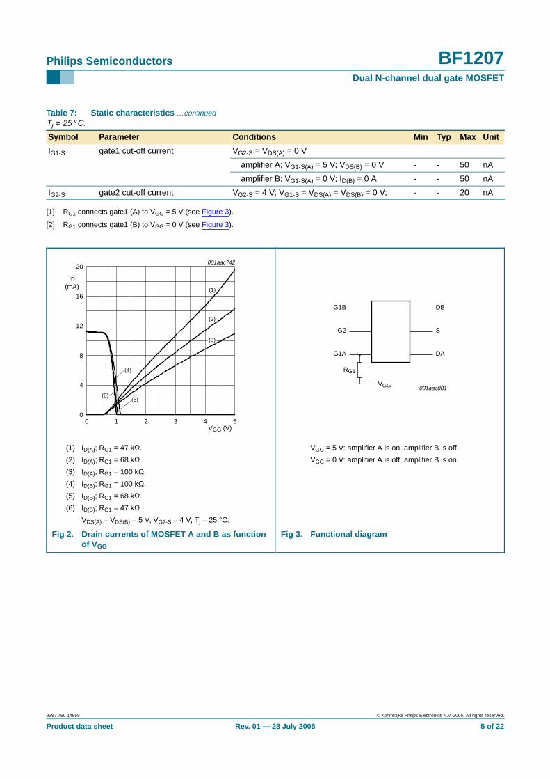
(1) ID(A); RG1 = 47 kΩ.
(2) ID(A); RG1 = 68 kΩ.
(3) ID(A); RG1 = 100 kΩ.
(4) ID(B); RG1 = 100 kΩ.
(5) ID(B); RG1 = 68 kΩ.
(6) ID(B); RG1 = 47 kΩ.
VDS(A) = VDS(B) = 5 V; VG2-S = 4 V; Tj = 25 °C.
VGG = 5 V: amplifier A is on; amplifier B is off.
VGG = 0 V: amplifier A is off; amplifier B is on.
Fig 2. Drain currents of MOSFET A and B as functionof VGG
Fig 3. Functional diagram
001aac742
8
12
4
16
20
ID(mA)
0
VGG (V)0 542 31
(2)
(5)
(4)
(6)
(3)
(1)
001aac881
RG1
VGG
G1A
G2
G1B
DA
S
DB
9397 750 14955 © Koninklijke Philips Electronics N.V. 2005. All rights reserved.
Product data sheet Rev. 01 — 28 July 2005 5 of 22

Philips Semiconductors BF1207Dual N-channel dual gate MOSFET
8. Dynamic characteristics
8.1 Dynamic characteristics for amplifier A
[1] For the MOSFET not in use: VG1-S(B) = 0 V; VDS(B) = 0 V.
[2] Measured in Figure 29 test circuit.
Table 8: Dynamic characteristics for amplifier ACommon source; Tamb = 25 °C; VG2-S = 4 V; VDS = 5 V; ID = 18 mA. [1]
Symbol Parameter Conditions Min Typ Max Unit
yfs forward transfer admittance Tj = 25 °C 25 30 40 mS
Ciss(G1) input capacitance at gate1 f = 100 MHz - 2.2 2.7 pF
Ciss(G2) input capacitance at gate2 f = 1 MHz - 3.5 - pF
Coss output capacitance f = 100 MHz - 0.9 - pF
Crss reverse transfer capacitance f = 100 MHz - 20 - fF
Gtr power gain BS = BS(opt); BL = BL(opt)
f = 200 MHz; GS = 2 mS; GL = 0.5 mS 30 34 38 dB
f = 400 MHz; GS = 2 mS; GL = 1 mS 26 30 34 dB
f = 800 MHz; GS = 3.3 mS; GL = 1 mS 21 25 29 dB
NF noise figure f = 11 MHz; GS = 20 mS; BS = 0 S - 3.0 - dB
f = 400 MHz; YS = YS(opt) - 1.3 - dB
f = 800 MHz; YS = YS(opt) - 1.4 - dB
Xmod cross-modulation input level for k = 1 %; fw = 50 MHz;funw = 60 MHz
[2]
at 0 dB AGC 90 - - dBµV
at 10 dB AGC - 90 - dBµV
at 20 dB AGC - 99 - dBµV
at 40 dB AGC 100 105 - dBµV
9397 750 14955 © Koninklijke Philips Electronics N.V. 2005. All rights reserved.
Product data sheet Rev. 01 — 28 July 2005 6 of 22

Philips Semiconductors BF1207Dual N-channel dual gate MOSFET
8.1.1 Graphs for amplifier A
(1) VG2-S = 4 V.
(2) VG2-S = 3.5 V.
(3) VG2-S = 3 V.
(4) VG2-S = 2.5 V.
(5) VG2-S = 2 V.
(6) VG2-S = 1.5 V.
(7) VG2-S = 1 V.
VDS(A) = 5 V; Tj = 25 °C.
(1) VG1-S(A) = 1.9 V.
(2) VG1-S(A) = 1.8 V.
(3) VG1-S(A) = 1.7 V.
(4) VG1-S(A) = 1.6 V.
(5) VG1-S(A) = 1.5 V.
(6) VG1-S(A) = 1.4 V.
(7) VG1-S(A) = 1.3 V.
(8) VG1-S(A) = 1.2 V.
(9) VG1-S(A) = 1.1 V.
VDS(A) = 5 V; VG2-S = 4 V; Tj = 25 °C.
Fig 4. Amplifier A: transfer characteristics; typicalvalues
Fig 5. Amplifier A: output characteristics; typicalvalues
VG1-S (V)0 2.01.60.8 1.20.4
001aac882
ID(mA)
15
5
10
20
30
25
35
0
(7)
(6)
(5)
(4)
(1)
(2)
(3)
001aaa883
VDS (V)0 642
16
8
24
32
ID(mA)
0
(2)
(3)
(6)
(9)
(8)
(5)
(1)
(4)
(7)
9397 750 14955 © Koninklijke Philips Electronics N.V. 2005. All rights reserved.
Product data sheet Rev. 01 — 28 July 2005 7 of 22
Philips Semiconductors BF1207Dual N-channel dual gate MOSFET
(1) VG2-S = 4 V.
(2) VG2-S = 3.5 V.
(3) VG2-S = 3 V.
(4) VG2-S = 2.5 V.
(5) VG2-S = 2 V.
(6) VG2-S = 1.5 V.
(7) VG2-S = 1 V.
VDS(A) = 5 V; Tj = 25 °C.
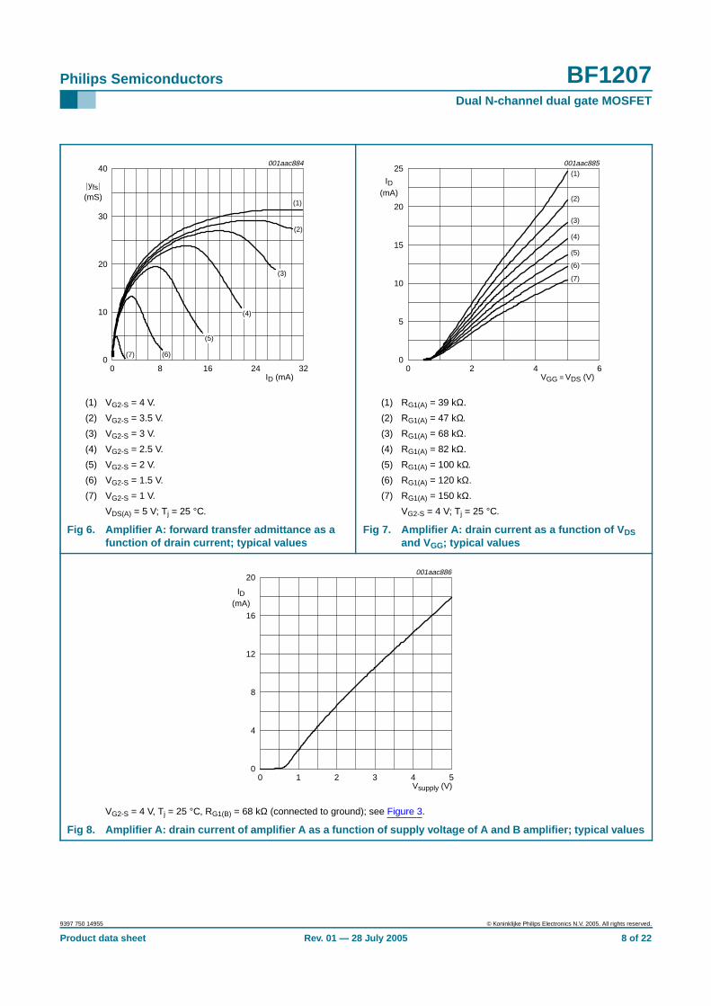
(1) RG1(A) = 39 kΩ.
(2) RG1(A) = 47 kΩ.
(3) RG1(A) = 68 kΩ.
(4) RG1(A) = 82 kΩ.
(5) RG1(A) = 100 kΩ.
(6) RG1(A) = 120 kΩ.
(7) RG1(A) = 150 kΩ.
VG2-S = 4 V; Tj = 25 °C.
Fig 6. Amplifier A: forward transfer admittance as afunction of drain current; typical values
Fig 7. Amplifier A: drain current as a function of V DSand VGG; typical values
VG2-S = 4 V, Tj = 25 °C, RG1(B) = 68 kΩ (connected to ground); see Figure 3.
Fig 8. Amplifier A: drain current of amplifier A as a function of supply voltage of A and B amplifier; typical values
ID (mA)0 32248 16
001aac884
20
10
30
40
yfs(mS)
0
(1)
(2)
(6)(7)
(5)
(4)
(3)
001aac885
VGG = VDS (V)0 642
ID(mA)
(1)
(2)
(3)
(4)
(5)
(7)
5
10
15
20
25
0
(6)
Vsupply (V)0 542 31
001aac886
8
12
4
16
20
ID(mA)
0
9397 750 14955 © Koninklijke Philips Electronics N.V. 2005. All rights reserved.
Product data sheet Rev. 01 — 28 July 2005 8 of 22

Philips Semiconductors BF1207Dual N-channel dual gate MOSFET
VDS(A) = VDS(B) = 5 V; VG1-S(B) = 0 V; fw = 50 MHz;funw = 60 MHz; Tamb = 25 °C; see Figure 29.
VDS(A) = VDS(B) = 5 V; VG1-S(B) = 0 V; f = 50 MHz;see Figure 29.
Fig 9. Amplifier A: unwanted voltage for 1 %cross-modulation as a function of gainreduction; typical values
Fig 10. Amplifier A: gain reduction as a function ofAGC voltage; typical values
VDS(A) = VDS(B) = 5 V; VG1-S(B) = 0 V; f = 50 MHz; Tamb = 25 °C; see Figure 29.
Fig 11. Amplifier A: drain current as a function of gain reduction; typical values
gain reduction (dB)0 504020 3010
001aac887
100
90
110
120
Vunw(dBµV)
80
VAGC (V)0 431 2
001aac888
30
20
40
10
0gain
reduction(dB)
50
gain reduction (dB)0 504020 3010
001aac889
ID(mA)
8
24
16
32
0
9397 750 14955 © Koninklijke Philips Electronics N.V. 2005. All rights reserved.
Product data sheet Rev. 01 — 28 July 2005 9 of 22
Philips Semiconductors BF1207Dual N-channel dual gate MOSFET
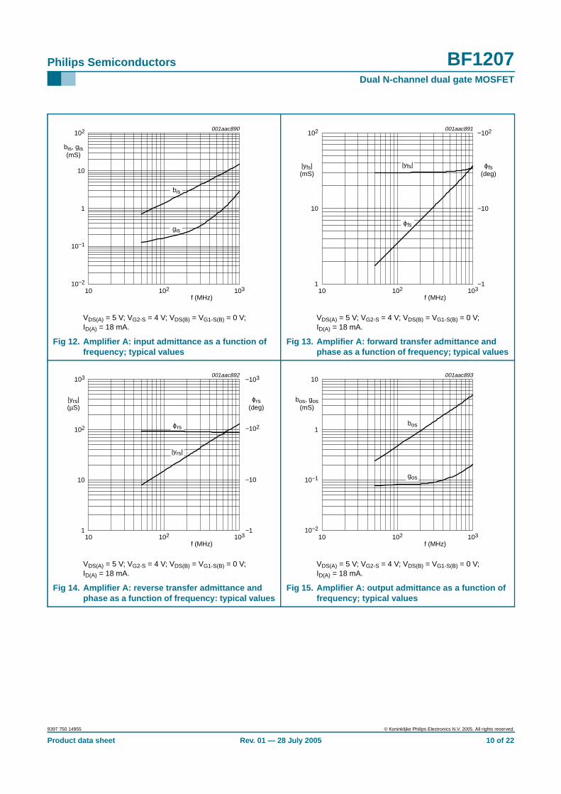
VDS(A) = 5 V; VG2-S = 4 V; VDS(B) = VG1-S(B) = 0 V;ID(A) = 18 mA.
VDS(A) = 5 V; VG2-S = 4 V; VDS(B) = VG1-S(B) = 0 V;ID(A) = 18 mA.
Fig 12. Amplifier A: input admittance as a function offrequency; typical values
Fig 13. Amplifier A: forward transfer admittance andphase as a function of frequency; typical values
VDS(A) = 5 V; VG2-S = 4 V; VDS(B) = VG1-S(B) = 0 V;ID(A) = 18 mA.
VDS(A) = 5 V; VG2-S = 4 V; VDS(B) = VG1-S(B) = 0 V;ID(A) = 18 mA.
Fig 14. Amplifier A: reverse transfer admittance andphase as a function of frequency: typical values
Fig 15. Amplifier A: output admittance as a function offrequency; typical values
001aac890
f (MHz)10 103102
10−1
1
10
102
bis, gis(mS)
10−2
bis
gis
f (MHz)10 103102
001aac891
10
102
|yfs|(mS)
1
−10
−102
ϕfs(deg)
−1
|yfs|
ϕfs
001aac892
102
10
103
|yrs|(µS)
1
f (MHz)10 103102
−102
−10
−103
ϕrs(deg)
−1
|yrs|
ϕrs
001aac893
1
10−1
10
bos, gos(mS)
10−2
f (MHz)10 103102
bos
gos
9397 750 14955 © Koninklijke Philips Electronics N.V. 2005. All rights reserved.
Product data sheet Rev. 01 — 28 July 2005 10 of 22
Philips Semiconductors BF1207Dual N-channel dual gate MOSFET
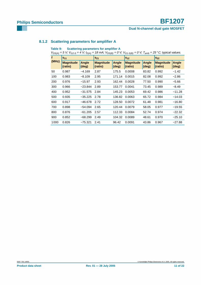
8.1.2 Scattering parameters for amplifier A
Table 9: Scattering parameters for amplifier AVDS(A) = 5 V; VG2-S = 4 V; ID(A) = 18 mA; VDS(B) = 0 V; VG1-S(B) = 0 V; Tamb = 25 °C; typical values.
f(MHz)
s11 s21 s12 s22
Magnitude(ratio)
Angle(deg)
Magnitude(ratio)
Angle(deg)
Magnitude(ratio)
Angle(deg)
Magnitude(ratio)
Angle(deg)
50 0.987 −4.169 2.87 175.5 0.0008 83.82 0.992 −1.42
100 0.983 −8.109 2.95 171.14 0.0015 82.08 0.992 −2.86
200 0.976 −15.97 2.93 162.44 0.0028 77.50 0.990 −5.66
300 0.966 −23.844 2.89 153.77 0.0041 73.45 0.989 −8.49
400 0.952 −31.575 2.84 145.23 0.0053 69.42 0.986 −11.28
500 0.935 −35.225 2.78 136.82 0.0063 65.72 0.984 −14.03
600 0.917 −46.678 2.72 128.50 0.0072 61.48 0.981 −16.80
700 0.898 −54.094 2.65 120.44 0.0079 58.05 0.977 −19.55
800 0.876 −61.205 2.57 112.33 0.0084 52.74 0.974 −22.32
900 0.852 −68.299 2.49 104.32 0.0089 48.61 0.970 −25.10
1000 0.826 −75.321 2.41 96.42 0.0091 43.86 0.967 −27.88
9397 750 14955 © Koninklijke Philips Electronics N.V. 2005. All rights reserved.
Product data sheet Rev. 01 — 28 July 2005 11 of 22

Philips Semiconductors BF1207Dual N-channel dual gate MOSFET
8.2 Dynamic characteristics for amplifier B
[1] For the MOSFET not in use: VG1-S(A) = 0 V; VDS(A) = 0 V.
[2] Measured in Figure 30 test circuit.
Table 10: Dynamic characteristics for amplifier BCommon source; Tamb = 25 °C; VG2-S = 4 V; VDS = 5 V; ID = 14 mA. [1]
Symbol Parameter Conditions Min Typ Max Unit
yfs forward transfer admittance Tj = 25 °C 26 31 41 mS
Ciss(G1) input capacitance at gate1 f = 100 MHz - 1.8 2.3 pF
Ciss(G2) input capacitance at gate2 f = 1 MHz - 3.5 - pF
Coss output capacitance f = 100 MHz - 0.8 - pF
Crss reverse transfer capacitance f = 100 MHz - 20 - fF
Gtr power gain BS = BS(opt); BL = BL(opt)
f = 200 MHz; GS = 2 mS; GL = 0.5 mS 30 34 38 dB
f = 400 MHz; GS = 2 mS; GL = 1 mS 27 31 35 dB
f = 800 MHz; GS = 3.3 mS; GL = 1 mS 23 27 31 dB
NF noise figure f = 11 MHz; GS = 20 mS; BS = 0 S - 5 - dB
f = 400 MHz; YS = YS(opt) - 1.3 - dB
f = 800 MHz; YS = YS(opt) - 1.4 - dB
Xmod cross-modulation input level for k = 1 %; fw = 50 MHz; funw = 60 MHz [2]
at 0 dB AGC 90 - - dBµV
at 10 dB AGC - 88 - dBµV
at 20 dB AGC - 94 - dBµV
at 40 dB AGC 100 103 - dBµV
9397 750 14955 © Koninklijke Philips Electronics N.V. 2005. All rights reserved.
Product data sheet Rev. 01 — 28 July 2005 12 of 22
Philips Semiconductors BF1207Dual N-channel dual gate MOSFET
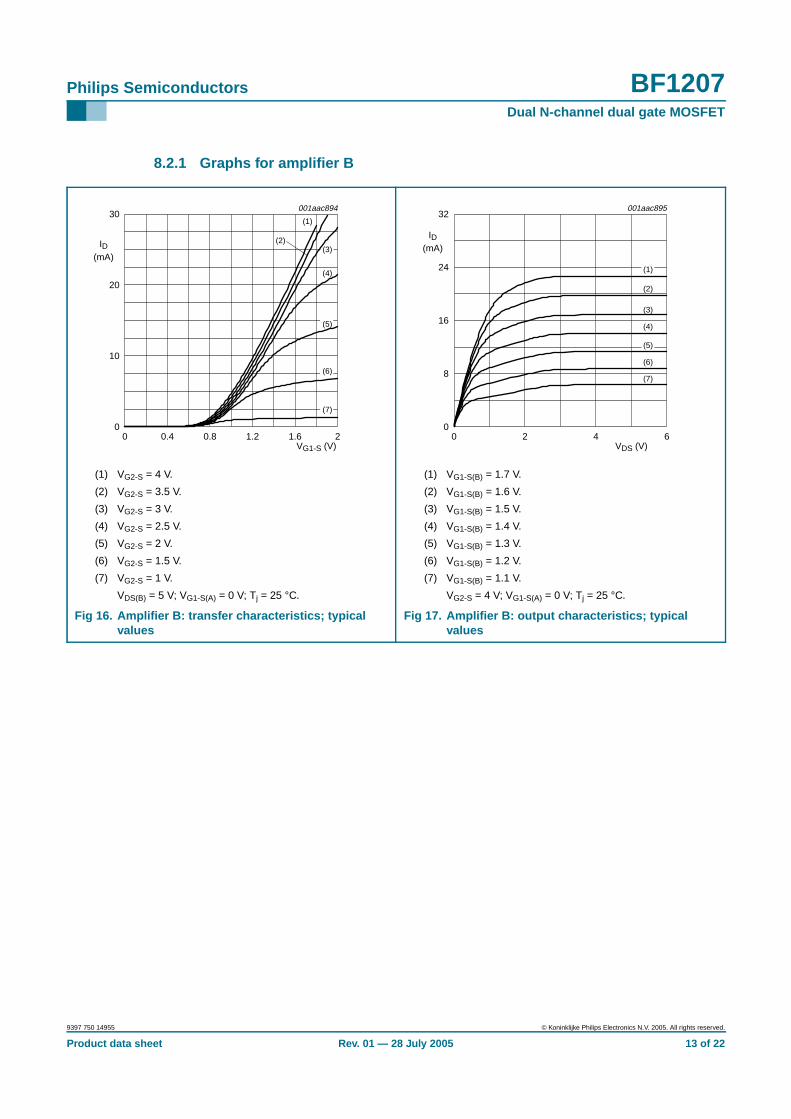
8.2.1 Graphs for amplifier B
(1) VG2-S = 4 V.
(2) VG2-S = 3.5 V.
(3) VG2-S = 3 V.
(4) VG2-S = 2.5 V.
(5) VG2-S = 2 V.
(6) VG2-S = 1.5 V.
(7) VG2-S = 1 V.
VDS(B) = 5 V; VG1-S(A) = 0 V; Tj = 25 °C.
(1) VG1-S(B) = 1.7 V.
(2) VG1-S(B) = 1.6 V.
(3) VG1-S(B) = 1.5 V.
(4) VG1-S(B) = 1.4 V.
(5) VG1-S(B) = 1.3 V.
(6) VG1-S(B) = 1.2 V.
(7) VG1-S(B) = 1.1 V.
VG2-S = 4 V; VG1-S(A) = 0 V; Tj = 25 °C.
Fig 16. Amplifier B: transfer characteristics; typicalvalues
Fig 17. Amplifier B: output characteristics; typicalvalues
VG1-S (V)0 21.60.8 1.20.4
001aac894
10
20
30
ID(mA)
0
(4)
(5)
(2)(3)
(1)
(7)
(6)
001aac895
VDS (V)0 642
16
8
24
32
ID(mA)
0
(2)
(6)
(7)
(4)
(3)
(5)
(1)
9397 750 14955 © Koninklijke Philips Electronics N.V. 2005. All rights reserved.
Product data sheet Rev. 01 — 28 July 2005 13 of 22
Philips Semiconductors BF1207Dual N-channel dual gate MOSFET
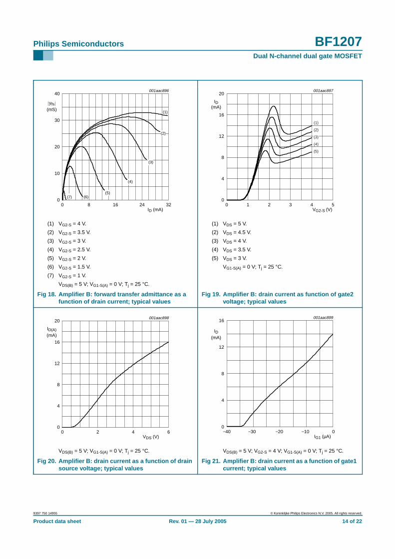
(1) VG2-S = 4 V.
(2) VG2-S = 3.5 V.
(3) VG2-S = 3 V.
(4) VG2-S = 2.5 V.
(5) VG2-S = 2 V.
(6) VG2-S = 1.5 V.
(7) VG2-S = 1 V.
VDS(B) = 5 V; VG1-S(A) = 0 V; Tj = 25 °C.
(1) VDS = 5 V.
(2) VDS = 4.5 V.
(3) VDS = 4 V.
(4) VDS = 3.5 V.
(5) VDS = 3 V.
VG1-S(A) = 0 V; Tj = 25 °C.
Fig 18. Amplifier B: forward transfer admittance as afunction of drain current; typical values
Fig 19. Amplifier B: drain current as function of gate2voltage; typical values
VDS(B) = 5 V; VG1-S(A) = 0 V; Tj = 25 °C. VDS(B) = 5 V; VG2-S = 4 V; VG1-S(A) = 0 V; Tj = 25 °C.
Fig 20. Amplifier B: drain current as a function of drainsource voltage; typical values
Fig 21. Amplifier B: drain current as a function of gate1current; typical values
ID (mA)0 32248 16
001aac896
20
10
30
40
yfs(mS)
0
(1)
(6)(5)
(4)
(3)
(2)
(7)
VG2-S (V)0 542 31
001aac897
8
12
4
16
20
ID(mA)
0
(1)
(2)
(3)
(4)
(5)
001aac898
VDS (V)0 642
8
12
4
16
20
ID(A)(mA)
0
IG1 (µA)−40 0−20 −10−30
001aac899
8
4
12
16
ID(mA)
0
9397 750 14955 © Koninklijke Philips Electronics N.V. 2005. All rights reserved.
Product data sheet Rev. 01 — 28 July 2005 14 of 22

Philips Semiconductors BF1207Dual N-channel dual gate MOSFET
VDS(B) = 5 V; VGG = 5 V; VDS(A) = VG1-S(A) = 0 V;RG1(B) = 150 kΩ (connected to VGG); fw = 50 MHz;funw = 60 MHz; Tamb = 25 °C; see Figure 30.
VDS(B) = 5 V; VGG = 5 V; VDS(A) = VG1-S(A) = 0 V;RG1(B) = 150 kΩ (connected to VGG); f = 50 MHz;Tamb = 25 °C; see Figure 30.
Fig 22. Amplifier B: unwanted voltage for 1 %cross-modulation as a function of gainreduction; typical values
Fig 23. Amplifier B: typical gain reduction as a functionof AGC voltage; typical values
VDS(B) = 5 V; VGG = 5 V; VDS(A) = VG1-S(A) = 0 V; RG1(B) = 150 kΩ (connected to VGG); f = 50 MHz; Tamb = 25 °C; seeFigure 30.
Fig 24. Amplifier B: drain current as a function of gain reduction; typical values
001aac900
gain reduction (dB)0 604020
100
90
110
120
Vunw(dBµV)
80
VAGC (V)0 431 2
001aac901
30
20
40
10
0gain
reduction(dB)
50
001aac902
gain reduction (dB)0 604020
8
12
4
16
20
ID(mA)
0
9397 750 14955 © Koninklijke Philips Electronics N.V. 2005. All rights reserved.
Product data sheet Rev. 01 — 28 July 2005 15 of 22

Philips Semiconductors BF1207Dual N-channel dual gate MOSFET
VDS(B) = 5 V; VG2-S = 4 V; VDS(A) = VG1-S(A) = 0 V;ID(B) = 14 mA.
VDS(B) = 5 V; VG2-S = 4 V; VDS(A) = VG1-S(A) = 0 V;ID(B) = 14 mA.
Fig 25. Amplifier B: input admittance as a function offrequency; typical values
Fig 26. Amplifier B: forward transfer admittance andphase as a function of frequency; typical values
VDS(B) = 5 V; VG2-S = 4 V; VDS(A) = VG1-S(A) = 0 V;ID(B) = 14 mA.
VDS(B) = 5 V; VG2-S = 4 V; VDS(A) = VG1-S(A) = 0 V;ID(B) = 14 mA.
Fig 27. Amplifier B: reverse transfer admittance andphase as a function of frequency; typical values
Fig 28. Amplifier B: output admittance as a function offrequency; typical values
001aac903
f (MHz)10 103102
10−1
1
10
102
bis, gis(mS)
10−2
bis
gis
f (MHz)10 103102
001aac904
10
102
|yfs|(mS)
1
−10
−102
ϕfs(deg)
−1
|yfs|
ϕfs
001aac905
102
10
103
|yrs|(µS)
1
−102
−10
−103
ϕrs(deg)
−1
f (MHz)10 103102
|yrs|
ϕrs
001aac906
1
10−1
10
bos, gos(mS)
10−2
f (MHz)10 103102
bos
gos
9397 750 14955 © Koninklijke Philips Electronics N.V. 2005. All rights reserved.
Product data sheet Rev. 01 — 28 July 2005 16 of 22

Philips Semiconductors BF1207Dual N-channel dual gate MOSFET
8.2.2 Scattering parameters for amplifier B
Table 11: Scattering parameters for amplifier BVDS(B) = 5 V; VG2-S = 4 V; ID(B) = 14 mA; VDS(A) = 0 V; VG1-S(A) = 0 V; Tamb = 25 °C; typical values.
f(MHz)
s11 s21 s12 s22
Magnitude(ratio)
Angle(deg)
Magnitude(ratio)
Angle(deg)
Magnitude(ratio)
Angle(deg)
Magnitude(ratio)
Angle(deg)
50 0.993 −3.018 3.07 176.04 0.0004 95.97 0.991 −1.39
100 0.992 −6.186 3.07 172.05 0.0011 90.33 0.990 −2.79
200 0.987 −12.43 3.09 164.13 0.0024 85.03 0.988 −5.49
300 0.979 −18.60 3.02 156.28 0.0036 82.94 0.986 −8.21
400 0.969 −24.62 2.99 148.48 0.0046 81.97 0.983 −10.91
500 0.957 −30.72 2.95 140.69 0.0056 81.03 0.980 −13.63
600 0.943 −36.71 2.90 132.87 0.0065 79.77 0.977 −16.40
700 0.927 −42.77 2.86 125.21 0.0074 79.04 0.973 −19.13
800 0.907 −48.91 2.79 117.22 0.0082 79.42 0.969 −21.93
900 0.885 −54.77 2.736 109.29 0.0086 75.47 0.964 −24.85
1000 0.858 −61.01 2.675 101.18 0.0092 73.48 0.958 −27.75
9397 750 14955 © Koninklijke Philips Electronics N.V. 2005. All rights reserved.
Product data sheet Rev. 01 — 28 July 2005 17 of 22

Philips Semiconductors BF1207Dual N-channel dual gate MOSFET
9. Test information
Fig 29. Cross-modulation test set-up for amplifier A
50 Ω
10 kΩ
RGEN50 Ω 50 Ω RG1
4.7 nF
4.7 nF
4.7 nF G2 S
G1A DA
DB
4.7 nF
4.7 nF
4.7 nF
G1B
BF1207
VGG5 V
VDS(A)5 V
VDS(B)5V
VAGC
L22.2 µH
L12.2 µH
RL50 Ω
001aac907
Vi
Fig 30. Cross-modulation test set-up for amplifier B
50 Ω
10 kΩ
RGEN50 Ω
RL50 Ω50 Ω
RG1
4.7 nF
4.7 nF
4.7 nF
G2 S
G1A DA
DB
4.7 nF
4.7 nF
4.7 nFG1B
BF1207
VGG0 V
VDS(A)5 V
VDS(B)5V
VAGC
L22.2 µH
L12.2 µH
001aac908
Vi
9397 750 14955 © Koninklijke Philips Electronics N.V. 2005. All rights reserved.
Product data sheet Rev. 01 — 28 July 2005 18 of 22
Philips Semiconductors BF1207Dual N-channel dual gate MOSFET
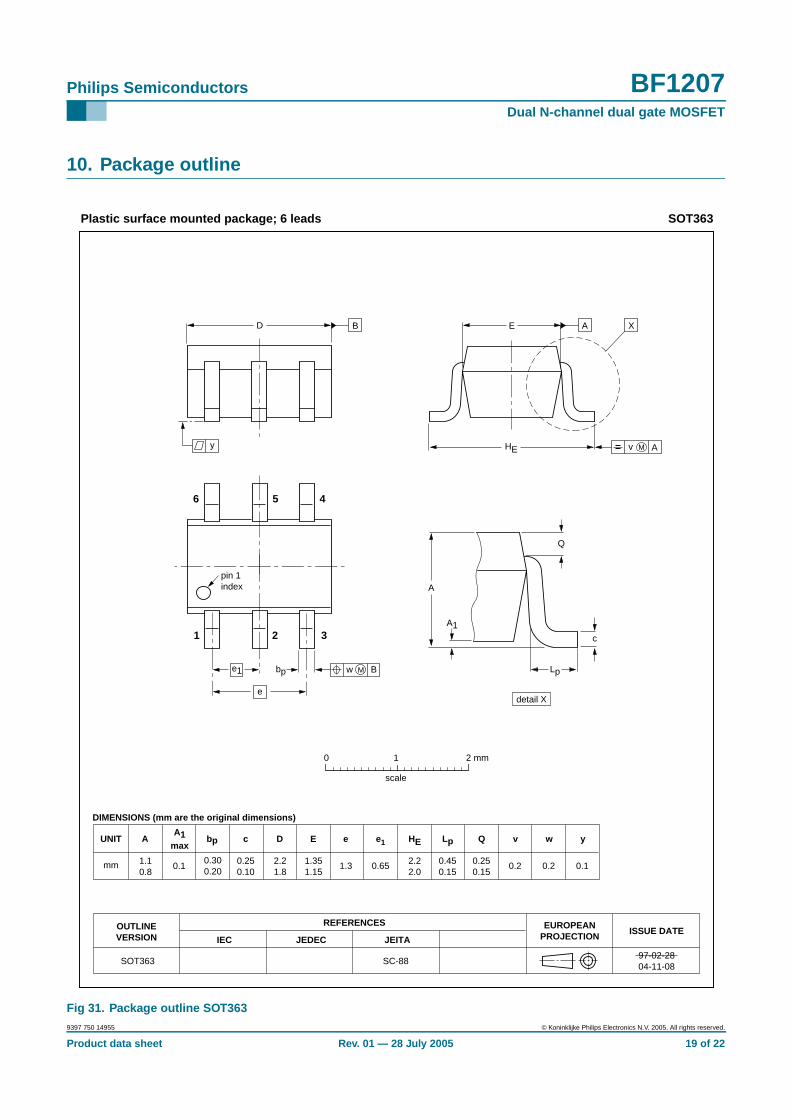
10. Package outline
Fig 31. Package outline SOT363
REFERENCESOUTLINEVERSION
EUROPEANPROJECTION ISSUE DATE
IEC JEDEC JEITA
SOT363 SC-88
w BMbp
D
e1
e
pin 1index A
A1
Lp
Q
detail X
HE
E
v M A
AB
y
0 1 2 mm
scale
c
X
1 32
456
Plastic surface mounted package; 6 leads SOT363
UNITA1
maxbp c D E e1 HE Lp Q ywv
mm 0.10.300.20
2.21.8
0.250.10
1.351.15
0.65
e
1.3 2.22.0
0.2 0.10.2
DIMENSIONS (mm are the original dimensions)
0.450.15
0.250.15
A
1.10.8
97-02-2804-11-08
9397 750 14955 © Koninklijke Philips Electronics N.V. 2005. All rights reserved.
Product data sheet Rev. 01 — 28 July 2005 19 of 22
Philips Semiconductors BF1207Dual N-channel dual gate MOSFET
11. Revision history
Table 12: Revision history
Document ID Release date Data sheet status Change notice Doc. number Supersedes
BF1207_1 20050728 Product data sheet - 9397 750 14955 -
9397 750 14955 © Koninklijke Philips Electronics N.V. 2005. All rights reserved.
Product data sheet Rev. 01 — 28 July 2005 20 of 22
Philips Semiconductors BF1207Dual N-channel dual gate MOSFET
12. Data sheet status
[1] Please consult the most recently issued data sheet before initiating or completing a design.
[2] The product status of the device(s) described in this data sheet may have changed since this data sheet was published. The latest information is available on the Internet atURL http://www.semiconductors.philips.com.
[3] For data sheets describing multiple type numbers, the highest-level product status determines the data sheet status.
13. Definitions
Short-form specification — The data in a short-form specification isextracted from a full data sheet with the same type number and title. Fordetailed information see the relevant data sheet or data handbook.
Limiting values definition — Limiting values given are in accordance withthe Absolute Maximum Rating System (IEC 60134). Stress above one ormore of the limiting values may cause permanent damage to the device.These are stress ratings only and operation of the device at these or at anyother conditions above those given in the Characteristics sections of thespecification is not implied. Exposure to limiting values for extended periodsmay affect device reliability.
Application information — Applications that are described herein for anyof these products are for illustrative purposes only. Philips Semiconductorsmake no representation or warranty that such applications will be suitable forthe specified use without further testing or modification.
14. Disclaimers
Life support — These products are not designed for use in life supportappliances, devices, or systems where malfunction of these products canreasonably be expected to result in personal injury. Philips Semiconductors
customers using or selling these products for use in such applications do soat their own risk and agree to fully indemnify Philips Semiconductors for anydamages resulting from such application.
Right to make changes — Philips Semiconductors reserves the right tomake changes in the products - including circuits, standard cells, and/orsoftware - described or contained herein in order to improve design and/orperformance. When the product is in full production (status ‘Production’),relevant changes will be communicated via a Customer Product/ProcessChange Notification (CPCN). Philips Semiconductors assumes noresponsibility or liability for the use of any of these products, conveys nolicense or title under any patent, copyright, or mask work right to theseproducts, and makes no representations or warranties that these products arefree from patent, copyright, or mask work right infringement, unless otherwisespecified.
15. Trademarks
Notice — All referenced brands, product names, service names andtrademarks are the property of their respective owners.
16. Contact information
For additional information, please visit: http://www.semiconductors.philips.com
For sales office addresses, send an email to: [email protected]
Level Data sheet status [1] Product status [2] [3] Definition
I Objective data Development This data sheet contains data from the objective specification for product development. PhilipsSemiconductors reserves the right to change the specification in any manner without notice.
II Preliminary data Qualification This data sheet contains data from the preliminary specification. Supplementary data will be publishedat a later date. Philips Semiconductors reserves the right to change the specification without notice, inorder to improve the design and supply the best possible product.
III Product data Production This data sheet contains data from the product specification. Philips Semiconductors reserves theright to make changes at any time in order to improve the design, manufacturing and supply. Relevantchanges will be communicated via a Customer Product/Process Change Notification (CPCN).
9397 750 14955 © Koninklijke Philips Electronics N.V. 2005. All rights reserved.
Product data sheet Rev. 01 — 28 July 2005 21 of 22
Philips Semiconductors BF1207Dual N-channel dual gate MOSFET
17. Contents
1 Product profile . . . . . . . . . . . . . . . . . . . . . . . . . . 11.1 General description. . . . . . . . . . . . . . . . . . . . . . 11.2 Features . . . . . . . . . . . . . . . . . . . . . . . . . . . . . . 11.3 Applications . . . . . . . . . . . . . . . . . . . . . . . . . . . 11.4 Quick reference data. . . . . . . . . . . . . . . . . . . . . 22 Pinning information . . . . . . . . . . . . . . . . . . . . . . 23 Ordering information . . . . . . . . . . . . . . . . . . . . . 34 Marking . . . . . . . . . . . . . . . . . . . . . . . . . . . . . . . . 35 Limiting values. . . . . . . . . . . . . . . . . . . . . . . . . . 36 Thermal characteristics. . . . . . . . . . . . . . . . . . . 47 Static characteristics. . . . . . . . . . . . . . . . . . . . . 48 Dynamic characteristics . . . . . . . . . . . . . . . . . . 68.1 Dynamic characteristics for amplifier A. . . . . . . 68.1.1 Graphs for amplifier A. . . . . . . . . . . . . . . . . . . . 78.1.2 Scattering parameters for amplifier A . . . . . . . 118.2 Dynamic characteristics for amplifier B. . . . . . 128.2.1 Graphs for amplifier B. . . . . . . . . . . . . . . . . . . 138.2.2 Scattering parameters for amplifier B . . . . . . . 179 Test information . . . . . . . . . . . . . . . . . . . . . . . . 1810 Package outline . . . . . . . . . . . . . . . . . . . . . . . . 1911 Revision history . . . . . . . . . . . . . . . . . . . . . . . . 2012 Data sheet status . . . . . . . . . . . . . . . . . . . . . . . 2113 Definitions . . . . . . . . . . . . . . . . . . . . . . . . . . . . 2114 Disclaimers. . . . . . . . . . . . . . . . . . . . . . . . . . . . 2115 Trademarks. . . . . . . . . . . . . . . . . . . . . . . . . . . . 2116 Contact information . . . . . . . . . . . . . . . . . . . . 21
© Koninklijke Philips Electronics N.V. 2005All rights are reserved. Reproduction in whole or in part is prohibited without the priorwritten consent of the copyright owner. The information presented in this document doesnot form part of any quotation or contract, is believed to be accurate and reliable and maybe changed without notice. No liability will be accepted by the publisher for anyconsequence of its use. Publication thereof does not convey nor imply any license underpatent- or other industrial or intellectual property rights.
Date of release: 28 July 2005Document number: 9397 750 14955
Published in The Netherlands


