Download - BF4-IR2 Series - HIROSE

BF4-IR2 Series
0.05~6.25 Gbps
Compact E/O,O/E Built-In Bidirectional IO Connector Design Note
(Specification)
Revision History
Version No.
Changed Points
0.9 Specifications preliminary version
1.0 First Edition(Official version)
COUNT DESCRIPTION OF REVISIONS DESIGNED CHECKED DATE
1 1 DIS-K-00002557 TH.KIKUCHI TS.YAMAZAKI 20201113
TITLE
BF4-IR2 Design note APPROVED YY.HIYAMA 20201005
CHECKED TS.YAMAZAKI 20201005
DESIGNED TH.KIKUCHI 20201005
WRITTEN SK.AOYAMA 20201005
TECHICAL SPECIFICATION ETAD-K0794-00 1 1 / 32
FORM HC0011-9-1
HIROSE ELECTRIC CO.,LTD.
△
△
Mar
.1.2
022
Cop
yrig
ht 2
022
HIR
OS
E E
LEC
TR
IC C
O.,
LTD
. All
Rig
hts
Res
erve
d.

HIROSE ELECTRIC CO., LTD. Document Number: ETAD-K0794 Revision 0.9
― Table of Contents ―
1. Introduction .................................................................................................................................... 4
1.1. Overview ................................................................................................................................. 4
1.2. Product Features ..................................................................................................................... 4
1.3. Application ............................................................................................................................... 4
1.4. Laser Class ............................................................................................................................. 4
2. Product Information ...................................................................................................................... 5
2.1. Product Number Creation ....................................................................................................... 5
2.2. Product Dimensions ................................................................................................................ 6
2.3. Product Materials .................................................................................................................. 10
2.4. Packaging Style .................................................................................................................... 12
2.5. Block Diagram ....................................................................................................................... 13
2.6. Pin Assignment ..................................................................................................................... 14
2.7. Pin Function .......................................................................................................................... 14
2.8. Recommended PCB Layout and Temperature Profile ......................................................... 15
2.9. Typical Layout ....................................................................................................................... 16
3. Operational Characteristics ....................................................................................................... 17
3.1. Absolute Maximum Rating .................................................................................................... 17
3.2. Recommended Operating Conditions ................................................................................... 17
3.3. DC Characteristics ................................................................................................................ 17
3.4. AC Characteristics ................................................................................................................ 18
3.5. Optical Characteristics .......................................................................................................... 18
4. Functional Description ................................................................................................................ 19
4.1. Functioning Confirmation LED .............................................................................................. 19
4.2. Termination Resistor(EO-DATA*+/-) ................................................................................ 19
4.3. DC Balance ........................................................................................................................... 20
4.4. Active/Sleep Mode Function(EO-ACT*) ................................................................................ 20
4.5. Signal Detect Function(OE-SD*n) ......................................................................................... 21
4.6. PD Current Monitoring Status Function(ANDATA*) .............................................................. 22
5. Typical Characteristics ............................................................................................................... 23
5.1. Eye Pattern by transmission speed ...................................................................................... 23
5.2. Characteristics variation in fiber length ................................................................................. 24
5.3. Temperature Characteristics ................................................................................................. 25
Mar
.1.2
022
Cop
yrig
ht 2
022
HIR
OS
E E
LEC
TR
IC C
O.,
LTD
. All
Rig
hts
Res
erve
d.
HIROSE ELECTRIC CO., LTD. Document Number: ETAD-K0794 Revision 0.9
6. Notes ............................................................................................................................................. 26
6.1. Fiber Optic Cable Handling ................................................................................................... 26
6.2. Countermeasures Against Static Electricity .......................................................................... 27
6.3. Connector Mating Method ..................................................................................................... 27
6.4. Connector Unmating Method ................................................................................................ 28
6.5. Fail-safe design ..................................................................................................................... 29
6.6. Notes On Handling the Product ............................................................................................ 30
6.7. Notes on the Use of the Product ........................................................................................... 31
7. Revision History .......................................................................................................................... 32
Mar
.1.2
022
Cop
yrig
ht 2
022
HIR
OS
E E
LEC
TR
IC C
O.,
LTD
. All
Rig
hts
Res
erve
d.

HIROSE ELECTRIC CO., LTD. Document Number: ETAD-K0794 Revision 0.9
- 4 -
11.. IInnttrroodduuccttiioonn
11..11.. OOvveerrvviieeww
Hirose has developed a bidirectional transmission type active optical connector for wiring inside
and between devices known as the BF4-IR2 Connector. By incorporating two BF4MC series
connectors into the plug side connector, it allows for significantly lower power consumption,
bending durable optical cables as well as the advantages of optical transmissions “long-distance
transmission, electromagnetic noiseless, and isolation” are all easily packaged inside of a
bidirectional, dual core optical transmission interface connector. It can be used in a wide range of
fields including medical equipment and industrial equipment.
11..22.. PPrroodduucctt FFeeaattuurreess
Using Optical Fibers to Achieve 6.25 Gbps High Speed Transmissions
Bidirectional Transmission
Built-In LED for Operational Confirmation (LED Color : Green/Amber)
Bending Durable Fiber
Low Power Consumption (160mW or Less/ Plug)
11..33.. AApppplliiccaattiioonn
E/O, O/E Conversion Data Transmission(High Speed, Isolated Transmission)
FPGA Application(Clock Transmission、Data Transmission[8B10B Encoded])
11..44.. LLaasseerr CCllaassss
This product has a built-in laser product that is classified as “Class 1 Laser Product” under the IEC 60825-1 Edition3.0 standard. Class 1 laser systems are generally considered safe to the human body. When using this product, please use specification that match those describe in this document and avoid use above specified ratings or disassembly of the product.
Mar
.1.2
022
Cop
yrig
ht 2
022
HIR
OS
E E
LEC
TR
IC C
O.,
LTD
. All
Rig
hts
Res
erve
d.
HIROSE ELECTRIC CO., LTD. Document Number: ETAD-K0794 Revision 0.9
- 5 -
22.. PPrroodduucctt IInnffoorrmmaattiioonn
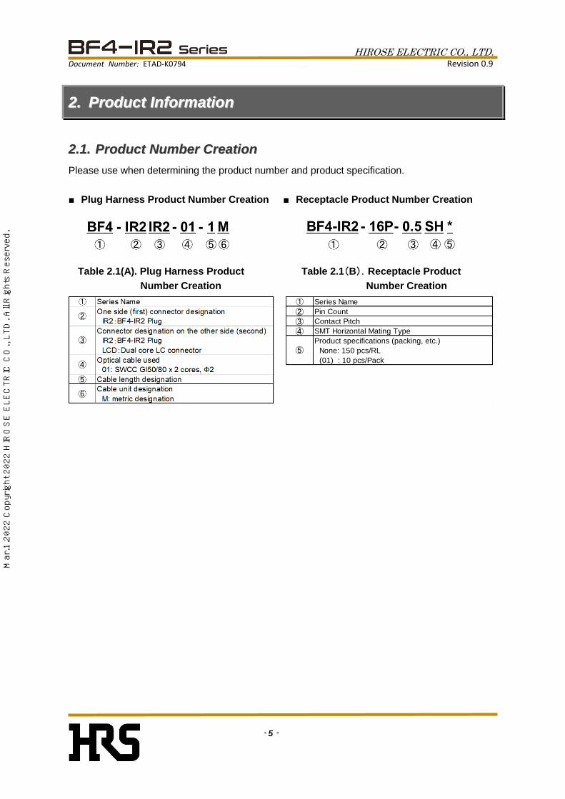
22..11.. PPrroodduucctt NNuummbbeerr CCrreeaattiioonn
Please use when determining the product number and product specification.
■ Plug Harness Product Number Creation ■ Receptacle Product Number Creation
Table 2.1(A). Plug Harness Product Table 2.1(B).Receptacle Product
Number Creation Number Creation
① Series Name
② Pin Count
③ Contact Pitch
④ SMT Horizontal Mating Type
Product specifications (packing, etc.)
None: 150 pcs/RL
(01) : 10 pcs/Pack
⑤
Mar
.1.2
022
Cop
yrig
ht 2
022
HIR
OS
E E
LEC
TR
IC C
O.,
LTD
. All
Rig
hts
Res
erve
d.

HIROSE ELECTRIC CO., LTD. Document Number: ETAD-K0794 Revision 0.9
- 6 -
22..22.. PPrroodduucctt DDiimmeennssiioonnss
■ Plug Harness:
・ Both Ends IR2 Plug Harness
Fig. 2.2(A).Both Ends IR2 Plug Harness
・ One End IR2 Plug-One End Dual LC Plug Harness (IR2-LC)
Fig. 2.2(B).One End IR2 Plug-One End Dual LC Plug Harness (IR2-LC)
Tabel 2.2(A).Plug harness product information
HRS No. Product Name Harness length L0831-1272-0 00 BF4-IR2IR2-01-1M 1m0831-1273-0 00 BF4-IR2LCD-01-1M 1m
Length(L) of the Plag harness :
・ We will do our best to accommodate harness lengths not listed above.
Please contact our sales department for the desired harness length.
Mar
.1.2
022
Cop
yrig
ht 2
022
HIR
OS
E E
LEC
TR
IC C
O.,
LTD
. All
Rig
hts
Res
erve
d.

HIROSE ELECTRIC CO., LTD. Document Number: ETAD-K0794 Revision 0.9
- 7 -
■ Plug
・ Plug Section(Expanded)
Fig. 2.2(C).Plug Section(Expanded)
・ Dual LC Plug(Expanded)
Fig. 2.2(D).Dual LC Plug(Expanded)
Mar
.1.2
022
Cop
yrig
ht 2
022
HIR
OS
E E
LEC
TR
IC C
O.,
LTD
. All
Rig
hts
Res
erve
d.
HIROSE ELECTRIC CO., LTD. Document Number: ETAD-K0794 Revision 0.9
- 8 -
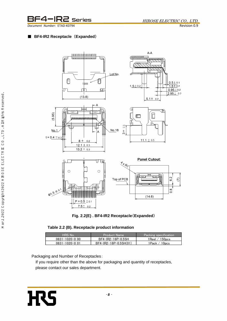
■ BF4-IR2 Receptacle (Expanded)
Fig. 2.2(E) . BF4-IR2 Receptacle(Expanded)
Table 2.2 (B). Receptacle product information
HRS No. Product Name Packing specification0831-1020-0 00 BF4-IR2-16P-0.5SH 1Reel / 150pcs0831-1020-0 01 BF4-IR2-16P-0.5SH(01) 1Pack / 10pcs
Packaging and Number of Receptacles:
If you require other than the above for packaging and quantity of receptacles,
please contact our sales department.
Mar
.1.2
022
Cop
yrig
ht 2
022
HIR
OS
E E
LEC
TR
IC C
O.,
LTD
. All
Rig
hts
Res
erve
d.

HIROSE ELECTRIC CO., LTD. Document Number: ETAD-K0794 Revision 0.9
- 9 -
■ Optical Fiber Cable(Cord)
Fig. 2.2(F).Optical Fiber Cable(Cord)
Table 2.2(C).Optical Fiber Cable (Cord) Detailed Information
Item Details
Fiber Type GI(50/80)
Material Silica Glass
Numerical Aperture (NA) 0.275±0.015 (*Note 1)
Core Diameter 50um
Clad Diameter 80um
Material UV Cureable Resin
Outer Diameter 165±10um
Color Red/Blue
Material Thermoplastic Resin
Outer Diameter 500um
Color Clear
Material Aramid Fiber (Kevlar)
Color Yellow
Material PVC
Cable Jacket Diameter 2.8mm
Color Orange
Tension Member
(Tensile Strength Member)
Cable Jacket
Primary Coating
Secondary Coating
Optical Fiber
*Note 1:Please contact our Fiber Optics Section for details on the Numerical
Aperture (NA) of the optical fiber.
Mar
.1.2
022
Cop
yrig
ht 2
022
HIR
OS
E E
LEC
TR
IC C
O.,
LTD
. All
Rig
hts
Res
erve
d.

HIROSE ELECTRIC CO., LTD. Document Number: ETAD-K0794 Revision 0.9
- 10 -
22..33.. PPrroodduucctt MMaatteerriiaallss
The BF4MC-IR2 plug harness product materials are indicated below in table 2.3.
Table 2.3 Plug Harness Product Materials
Details
Housing PBT(Black)
Printed Circuit Board FR-4
BF4-TX-14DS-0.5V PCB Mounting (*Note 2)
BF4-RX-14DS-0.5V PCB Mounting (*Note 2)
Insulation Case PA
Lock Plate Steel Alloy
Contact Copper Alloy
Shell Steel Alloy
Cable Clamp Copper Alloy
Clamp Ring Aluminium Alloy
Heat Shrink Tube Polyolefin
Light Guide Plate PC
Boots Polyester Elastomer (Blue)
Housing PEI(Beige)
Extender Cap PEI(Beige), Aluminium Alloy
LC Ferrule Zirconia、Steel Alloy
Spring Steel Alloy
Side Clip PP(Beige)
Boots Polyester Elastomer (Blue)
Boots Holder Copper Alloy
Cable Clamp Copper Alloy
Clamp Ring Copper Alloy
Heat Shrink Tube Polyolefin (Black)
Cap PP(Black)
BF4MC-6GTXP-1 (*Note 2)
BF4MC-6GRXP-1 (*Note 2)
Lens Protector Copper Alloy(Ni Plating)
Fixing Ring Copper Alloy
Optical Cord Materials Below (*Note 3)
-Optical Fiber Quartz Fiber(GI50/80)
-Primary Coating UV Cureable Resin
-Secondary Coating Thermoplastic Resin
-Tension Member Aramid Fiber (Kevlar)
-Outer Jacket PVC(Orange)
Parts
IR2 Plug
LC Plug
Optical Fiber Cord
*Note 2:In regards to the BF4MC Plug Harness/Receptacle
please reference the BF4MC design note (ETAD-K0671).
*Note 3:The optical fiber is coated with a dibutyltin compound (DBT) intentionally
added as a catalyst within the range of the REACH regulation value
(1000PPM tin conversion).
Mar
.1.2
022
Cop
yrig
ht 2
022
HIR
OS
E E
LEC
TR
IC C
O.,
LTD
. All
Rig
hts
Res
erve
d.
HIROSE ELECTRIC CO., LTD. Document Number: ETAD-K0794 Revision 0.9
- 11 -
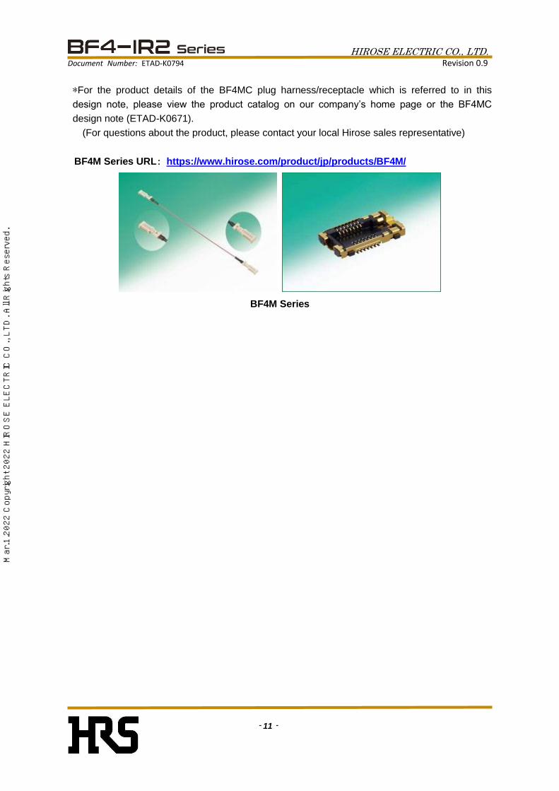
*For the product details of the BF4MC plug harness/receptacle which is referred to in this
design note, please view the product catalog on our company’s home page or the BF4MC
design note (ETAD-K0671).
(For questions about the product, please contact your local Hirose sales representative)
BF4M Series URL: https://www.hirose.com/product/jp/products/BF4M/
BF4M Series
Mar
.1.2
022
Cop
yrig
ht 2
022
HIR
OS
E E
LEC
TR
IC C
O.,
LTD
. All
Rig
hts
Res
erve
d.

HIROSE ELECTRIC CO., LTD. Document Number: ETAD-K0794 Revision 0.9
- 12 -
22..44.. PPaacckkaaggiinngg SSttyyllee
■ Plug harness packing form
・Individual Product Packaging
The product will be individually placed into an anti-static plastic bag and the bag will be sealed
closed.
・Packaging Box
The packing box will be a standard Hirose cardboard box and the size and shape will be
determined by the product type and the size of the order.
・Cushioning Material
Inside the packing box will be an anti-static air cap cushioning material.
■ Receptacle packing form (reel ,pack and embossed shape)
Figure 2.4 (A).Shape of a Reel Figure 2.4 (B).Shape of a Pack
Figure 2.4 (C).Taping direction
Figure 2.4(D).Embossed packaging
Mar
.1.2
022
Cop
yrig
ht 2
022
HIR
OS
E E
LEC
TR
IC C
O.,
LTD
. All
Rig
hts
Res
erve
d.

HIROSE ELECTRIC CO., LTD. Document Number: ETAD-K0794 Revision 0.9
- 13 -
22..55.. BBlloocckk DDiiaaggrraamm
The BF4MC-IR2 plug block diagram is described below in fig. 2.5.
*For details on the BF4MC-IR2 plugs internal BF4MC-TX/RX, please refer to the BF4MC design
note.
Fig. 2.5. IR2 Plug Block Diagram
Mar
.1.2
022
Cop
yrig
ht 2
022
HIR
OS
E E
LEC
TR
IC C
O.,
LTD
. All
Rig
hts
Res
erve
d.

HIROSE ELECTRIC CO., LTD. Document Number: ETAD-K0794 Revision 0.9
- 14 -
22..66.. PPiinn AAssssiiggnnmmeenntt
■ BF4-IR2 Pin Assignment
The BF4-IR2 plug/receptacle pin assignment is displayed below in fig. 2.6.
BF4-IR2 Plug Pin Assignment BF4-IR2 Receptacle Pin Assignment
Fig. 2.6.IR2 Plug/Receptacle Pin Assignment
22..77.. PPiinn FFuunnccttiioonn
The IR2 Plug Pin description is detailed below in table 2.7.
*I/O Notation (Type) is the direction that can be seen on the IR2 plug.
Table 2.7.IR2 Plug Pin Description
Pin No Symbol Name Type Details
1 VDD Vsupply Power
2 VDD Vsupply Power
3 GRN-LEDn Green LED Control InputGreen LED emission control
0V: Emitting, 3.3V: Not emitting
4 OE-SDn OE Signal Detect OutputOE signal detect status
0:Detected, 1:Undetected (+3.3V CMOS)
5 ANDATA Analog Data Output PD current monitor of OE module
6 GND Ground Ground Ground
7 OE-DATA- OE Data Output- Output
8 OE-DATA+ OE Data Output+ Output
9 GND Ground Ground Ground
10 EO-DATA- EO Data Input- Input
11 EO-DATA+ EO Data Input+ Input
12 GND Ground Ground Ground
13 EO-ACT EO Active Detect Input 1:Active Mode 0: Sleep (+3.3V CMOS )
14 EO-ACTn EO Active OutputEO active detect status
0:Detected.1:Undetected
15 AMB-LEDn Amber LED control InputAmber LED emission control
0: Emitting, 1: Not emitting(+3.3V CMOS)
16 NC NC - Non Connect Pin
Power Supply +3.3V
SLVS output
SLVS input
Mar
.1.2
022
Cop
yrig
ht 2
022
HIR
OS
E E
LEC
TR
IC C
O.,
LTD
. All
Rig
hts
Res
erve
d.

HIROSE ELECTRIC CO., LTD. Document Number: ETAD-K0794 Revision 0.9
- 15 -
22..88.. RReeccoommmmeennddeedd PPCCBB LLaayyoouutt aanndd TTeemmppeerraattuurree PPrrooffiillee
■ Recommended PCB Layout
Recommended PCB Land pattern dimensions Recommended metal mask dimensions
(PCB Thickness: 2.4mm) (Mask Thickness : 120 µm)
Fig. 2.8(A).Land pattern and metal mask recommended for BF4-IR2 receptacles
■ Recommended Temperature Profile
The maximum reflow temperature condition (Connector`s Upper Surface Temperature)
and recommended temperature reflow profile (Lead Free Solder) are described below in
Fig 2.8(B) and Fig 2.8(C).
Fig.2.8(B).Maximum Reflow Temperature Fig.2.8(C).Recommended Reflow
Conditions Temperature Profile
(Connector`s Upper Surface) (Lead Free Solder)
Mar
.1.2
022
Cop
yrig
ht 2
022
HIR
OS
E E
LEC
TR
IC C
O.,
LTD
. All
Rig
hts
Res
erve
d.
HIROSE ELECTRIC CO., LTD. Document Number: ETAD-K0794 Revision 0.9
- 16 -
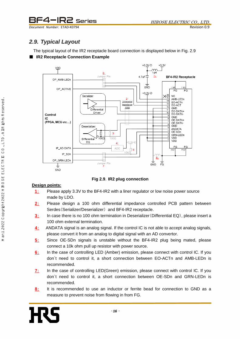
22..99.. TTyyppiiccaall LLaayyoouutt
The typical layout of the IR2 receptacle board connection is displayed below in Fig. 2.9
■ IR2 Receptacle Connection Example
Fig 2.9.IR2 plug connection
Design points:
1: Please apply 3.3V to the BF4-IR2 with a liner regulator or low noise power source
made by LDO.
2: Please design a 100 ohm differential impedance controlled PCB pattern between
Serdes(Serializer/Deserializer) and BF4-IR2 receptacle.
3: In case there is no 100 ohm termination in Deserializer(Differential EQ), please insert a
100 ohm external termination.
4: ANDATA signal is an analog signal. If the control IC is not able to accept analog signals,
please convert it from an analog to digital signal with an AD convertor.
5: Since OE-SDn signals is unstable without the BF4-IR2 plug being mated, please
connect a 10k ohm pull up resistor with power source.
6: In the case of controlling LED (Amber) emission, please connect with control IC. If you
don`t need to control it, a short connection between EO-ACTn and AMB-LEDn is
recommended.
7: In the case of controlling LED(Green) emission, please connect with control IC. If you
don`t need to control it, a short connection between OE-SDn and GRN-LEDn is
recommended.
8: It is recommended to use an inductor or ferrite bead for connection to GND as a
measure to prevent noise from flowing in from FG.
Mar
.1.2
022
Cop
yrig
ht 2
022
HIR
OS
E E
LEC
TR
IC C
O.,
LTD
. All
Rig
hts
Res
erve
d.

HIROSE ELECTRIC CO., LTD. Document Number: ETAD-K0794 Revision 0.9
- 17 -
33.. OOppeerraattiioonnaall CChhaarraacctteerriissttiiccss
33..11.. AAbbssoolluuttee MMaaxxiimmuumm RRaattiinngg
Table 3.1. IR2 plug harnesses absolute maximum rating.
Symbol Parameter Min Max Unit
VDD Maximum supply voltage - 0.3 + 4.5 V
VDIN Maximum voltage at EO-DATA +/- - 0.3 + 1.8 V
VACT Maximum voltage at EO-ACT - 0.3 + 3.6 V
S-Temp Storage temperature range - 40 + 85 ℃
VESD Electrostatic discharge voltage capability - 2 kV
*Note 4:Value when a discharge is applied to each pin.
*When using, please design the circuit so that the absolute maximum rated value listed
about in table 3.1 is not exceeded.
33..22.. RReeccoommmmeennddeedd OOppeerraattiinngg CCoonnddiittiioonnss
Table 3.2.IR2 Plug Harness Recommended Operating Conditions
Symbol Parameter Conditions Min Typ Max Unit
VDD Supply voltage + 3.0 + 3.3 + 3.6 V
GND Ground Level 0 + 0.4 V
Vnoise Maximum allowed supply noise on Supply 0 < fnoise < 10 GHz 100 mVpp
Temp Operating temperature range - 10 + 85 ℃
33..33.. DDCC CChhaarraacctteerriissttiiccss
Each IR2 plug`s DC characteristics are displayed below in table 3.3.
Table 3.3.IR2 Plug`s DC Characteristics
Symbol Parameter Conditions Min Typ Max Unit
VDD Supply volyage + 3.0 + 3.3 + 3.6 V
IDD Supply current VDD = +3.3V, Temp = 25℃ 80 mA
Bidirectional sleep. (All sleep) 50 uA
TX sleep ( Non active ) 45 mA
RX sleep ( No signale detect ) 35 mA
Vact_H Activation high input voltage level (high = "1") 1.0 VDD V
Vact_L Activation low input voltage level (low = "0") 0 + 0.4 V
Vsdn_H SD output voltage logic level high (high = "1") No signale detect + 3.0 VDD V
Vsdn_L SD output voltage logic level low (low = "0") Signal detect 0 + 0.4 V
Andata Mirrored photodiode current montor Operating at 6.25Gbps data input 40 mV
Isleep Sleep Mode Supply Current
*Note 5:Regarding the minimum output value of Andata.
Regardless of whether the BF4-IR2 plug is normal or abnormal, it may drop below 40 [mV] due to
loss of the relay cable. The output required for normal operation is 40 [mV] or more, so be careful
of the Andata value when using it.
*Note 4
*Note 5
Mar
.1.2
022
Cop
yrig
ht 2
022
HIR
OS
E E
LEC
TR
IC C
O.,
LTD
. All
Rig
hts
Res
erve
d.

HIROSE ELECTRIC CO., LTD. Document Number: ETAD-K0794 Revision 0.9
- 18 -
33..44.. AACC CChhaarraacctteerriissttiiccss
Each IR2 plug`s AC characteristics are displayed below in table 3.4.
Table 3.4.IR2 Plug`s AC Characteristics
Symbol Parameter Conditions Min Typ Max Unit
BR Bit rate 8B10B 0.05 6.25 Gbps
VCM_IN Input common mode voltage IR2 internal AC coupling (0.1uF) mV
200 1400 mVp
400 2800 mVp-p
ZIN Differential input impedance at Din+ and Din- 100 ohm
tD_ACT Activation delay time 500 us
tD_DEACT De-activation delay time 50 us
BER Bit error rate BR = 6.25Gbps, 8B10B PRBS7 10-12
tr Output data rise time 20%-80% 45 ps
tf Output data fall time 20%-80% 45 ps
VO_CM Output common mode voltage IR2 internal AC coupling (0.1uF) mV
160 330 mVp
320 660 mVp-p
VO_H Single ended output high voltage 660 mV
JP Jitter peak to peak BR = 6.25Gbps, 8B10B PRBS7 65 ps
ZO Output impedance at DOUT+/- 100 ohm
tSD_AT SD assert time 0.5 us
tSD_DT SD de-assert time 50 us
|VO_Diff| Output voltage swing
0
|VIN_Diff| Differential input voltage
0
33..55.. OOppttiiccaall CChhaarraacctteerriissttiiccss
Each IR2 plug`s optical characteristics are displayed below in table 3.5.
Table 3.5. IR2 LC Plug Harness Optical Characteristics Symbol Parameter Conditions Min Typ Max Unit
PAVE Average Launch Power (Transmitter) T=25 ℃ (LC Plug) 182 uW
λ Optical Wavelength (Transmitter) (LC Plug) 850 nm
R Responsivity (Receiver) λ=850nm (LC Plug) 0.35 A/W
Mar
.1.2
022
Cop
yrig
ht 2
022
HIR
OS
E E
LEC
TR
IC C
O.,
LTD
. All
Rig
hts
Res
erve
d.

HIROSE ELECTRIC CO., LTD. Document Number: ETAD-K0794 Revision 0.9
- 19 -
44.. FFuunnccttiioonnaall DDeessccrriippttiioonn
The BF4-IR2 series main function is described below.
44..11.. FFuunnccttiioonniinngg CCoonnffiirrmmaattiioonn LLEEDD
As a recommended usage,
On the board, short the 14th pin (AMB-LEDn) and 13th pin (EO-ACTn) of the IR2 receptacle and
short the 3rd pin (GRN_LEDn) and 4th pin (OR-SDn) of the plug. By doing so, you can check the
operating status of the plug with the LED.
In case of the above recommended connection,
LED (Amber) lights when ACTIVE signal is ON (High=+3.3V), and LED (Green) lights when SDn
signal (*Note 6) is ON (Low=0V).
*Note6:Confirmation about received signals or optical fiber disconnection can be done but,
data confirmation cannot be done. For actual data confirmation, the customer will have to
confirm it is correct.
Fig. 4.1.Operational Confirmation LED
44..22.. TTeerrmmiinnaattiioonn RReessiissttoorr((EEOO--DDAATTAA**++//--))
The IR2 plug has a built-in 100Ω termination resistor in the differential input section
(EO-DATA*+/-).
Fig. 4.2.Termination Resistor
Mar
.1.2
022
Cop
yrig
ht 2
022
HIR
OS
E E
LEC
TR
IC C
O.,
LTD
. All
Rig
hts
Res
erve
d.
HIROSE ELECTRIC CO., LTD. Document Number: ETAD-K0794 Revision 0.9
- 20 -
44..33.. DDCC BBaallaannccee
The data transmission of the BF4-IR2 series demonstrates the best performance by inputting
DC balanced signals. For the encoding format, 8B/10B is recommended (*Note 7).
Fig. 4.3.DC Balance(Encoding Format 8B/10B)
*Note 7:In regards to 8B/10B Encoding,
In 8-bit data, all are "0", but by executing 8B / 10B conversion (Encoding), symbols
where "0" and "1" are not consecutive for 5 bits or more can be obtained.
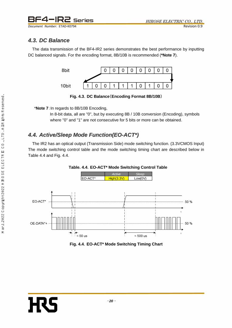
44..44.. AAccttiivvee//SSlleeeepp MMooddee FFuunnccttiioonn((EEOO--AACCTT**))
The IR2 has an optical output (Transmission Side) mode switching function. (3.3VCMOS Input)
The mode switching control table and the mode switching timing chart are described below in
Table 4.4 and Fig. 4.4.
Table. 4.4.EO-ACT* Mode Switching Control Table
Active Sleep
EO-ACT* High(3.3V) Low(0V)
Fig. 4.4.EO-ACT* Mode Switching Timing Chart
Mar
.1.2
022
Cop
yrig
ht 2
022
HIR
OS
E E
LEC
TR
IC C
O.,
LTD
. All
Rig
hts
Res
erve
d.

HIROSE ELECTRIC CO., LTD. Document Number: ETAD-K0794 Revision 0.9
- 21 -
44..55.. SSiiggnnaall DDeetteecctt FFuunnccttiioonn((OOEE--SSDD**nn))
The IR2 has an optical input detection status function for optical input (Receiver Side).
(3.3VCMOS Output) The optical input detection status table and EO-ACT*-OE-SD*n timing
charts are shown below in table 4.5 and Fig. 4.5(*Note 8).
Table 4.5.Optical Input detection Status Table
Detect Un-detect
OE-SD*n Low(0V) High(3.3V)
Fig. 4.6.EO-ACT*-OE-SD*n Timing Chart
*Note 8:In regards to SD*n, the reason why the logic is reversed from the BF4MC design note
(ETAD-K0671) is because the level is converted from + 1.5V to + 3.3V with a transistor.
(SD = 1.5V => SDn = 3.3V)
Mar
.1.2
022
Cop
yrig
ht 2
022
HIR
OS
E E
LEC
TR
IC C
O.,
LTD
. All
Rig
hts
Res
erve
d.
HIROSE ELECTRIC CO., LTD. Document Number: ETAD-K0794 Revision 0.9
- 22 -
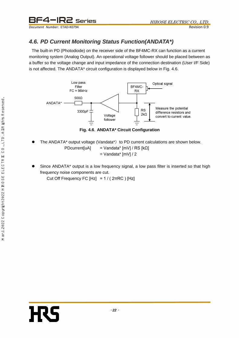
44..66.. PPDD CCuurrrreenntt MMoonniittoorriinngg SSttaattuuss FFuunnccttiioonn((AANNDDAATTAA**))
The built-in PD (Photodiode) on the receiver side of the BF4MC-RX can function as a current
monitoring system (Analog Output). An operational voltage follower should be placed between as
a buffer so the voltage change and input impedance of the connection destination (User I/F Side)
is not affected. The ANDATA* circuit configuration is displayed below in Fig. 4.6.
Fig. 4.6.ANDATA* Circuit Configuration
The ANDATA* output voltage (Vandata*) to PD current calculations are shown below.
PDcurrent[uA] = Vandata* [mV] / RS [kΩ]
= Vandata* [mV] / 2
Since ANDATA* output is a low frequency signal, a low pass filter is inserted so that high
frequency noise components are cut.
Cut Off Frequency FC [Hz] = 1 / ( 2πRC ) [Hz]
Mar
.1.2
022
Cop
yrig
ht 2
022
HIR
OS
E E
LEC
TR
IC C
O.,
LTD
. All
Rig
hts
Res
erve
d.
HIROSE ELECTRIC CO., LTD. Document Number: ETAD-K0794 Revision 0.9
- 23 -
55.. TTyyppiiccaall CChhaarraacctteerriissttiiccss
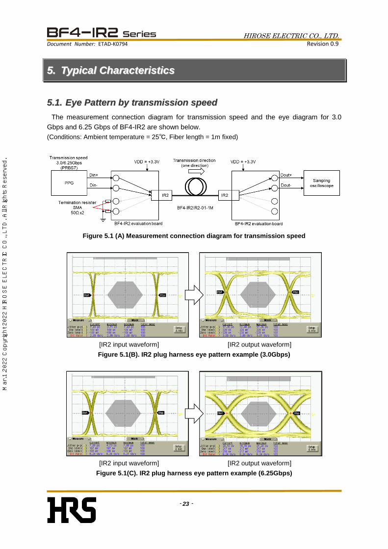
55..11.. EEyyee PPaatttteerrnn bbyy ttrraannssmmiissssiioonn ssppeeeedd
The measurement connection diagram for transmission speed and the eye diagram for 3.0
Gbps and 6.25 Gbps of BF4-IR2 are shown below.
(Conditions: Ambient temperature = 25℃, Fiber length = 1m fixed)
Figure 5.1 (A) Measurement connection diagram for transmission speed
[IR2 input waveform] [IR2 output waveform]
Figure 5.1(B). IR2 plug harness eye pattern example (3.0Gbps)
[IR2 input waveform] [IR2 output waveform]
Figure 5.1(C). IR2 plug harness eye pattern example (6.25Gbps)
Mar
.1.2
022
Cop
yrig
ht 2
022
HIR
OS
E E
LEC
TR
IC C
O.,
LTD
. All
Rig
hts
Res
erve
d.
HIROSE ELECTRIC CO., LTD. Document Number: ETAD-K0794 Revision 0.9
- 24 -
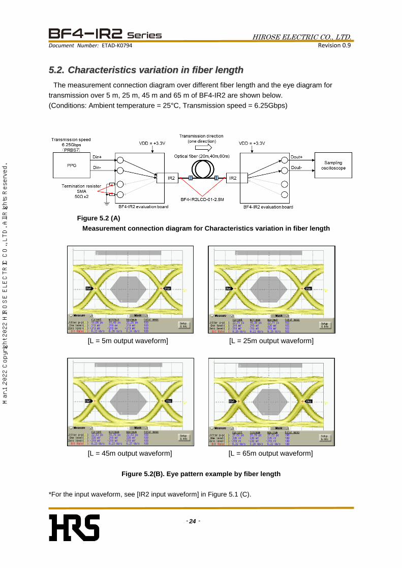
55..22.. CChhaarraacctteerriissttiiccss vvaarriiaattiioonn iinn ffiibbeerr lleennggtthh
The measurement connection diagram over different fiber length and the eye diagram for
transmission over 5 m, 25 m, 45 m and 65 m of BF4-IR2 are shown below.
(Conditions: Ambient temperature = 25°C, Transmission speed = 6.25Gbps)
Figure 5.2 (A)
Measurement connection diagram for Characteristics variation in fiber length
[L = 5m output waveform] [L = 25m output waveform]
[L = 45m output waveform] [L = 65m output waveform]
Figure 5.2(B). Eye pattern example by fiber length
*For the input waveform, see [IR2 input waveform] in Figure 5.1 (C).
Mar
.1.2
022
Cop
yrig
ht 2
022
HIR
OS
E E
LEC
TR
IC C
O.,
LTD
. All
Rig
hts
Res
erve
d.

HIROSE ELECTRIC CO., LTD. Document Number: ETAD-K0794 Revision 0.9
- 25 -
55..33.. TTeemmppeerraattuurree CChhaarraacctteerriissttiiccss
The measurement connection diagram of the temperature performance and the eye diagram for
transmission at the ambient temperature of -10C and +85C of BF4MC are shown below.
(Conditions: Fiber length = 1m, Transmission speed = 6.25 Gbps)
Figure 5.3(A). Measurement connection diagram for temperature characteristics
[Low temperature -10℃] [High temperature +85℃]
Figure 5.3(B). Temperature characteristics eye pattern example
*For the input waveform, see [IR2 input waveform] in Figure 5.1 (C).
Mar
.1.2
022
Cop
yrig
ht 2
022
HIR
OS
E E
LEC
TR
IC C
O.,
LTD
. All
Rig
hts
Res
erve
d.
HIROSE ELECTRIC CO., LTD. Document Number: ETAD-K0794 Revision 0.9
- 26 -
66.. NNootteess
This product uses an optical fiber as a transmission medium. The optical fiber is made
of quartz glass and requires more careful handling compared to an electric wire of the
same size. In addition, precautions should be made against static electricity since the
BF4MC-TX/RX plugs are equipped with internal semiconductor chips.
66..11.. FFiibbeerr OOppttiicc CCaabbllee HHaannddlliinngg
Sudden bending、excessive tensile stress、stress from external lateral pressure applied to
Fiber Optic cable may affect the functional performance of the product.
Optical Fiber Bending Radius
Fiber optical cable bending radius will have an influence over the failure rate (Lifetime).
When wiring, if there is a sudden bending there is a possibility of shortening the products
life so, wiring with a bending radius of over 10 mm is recommended (Devices Internal
Assembly).
Optical Fiber Bending Tension
It is recommended to wire the fiber (for arrangement within a device) so that tensile
stress is not applied to bent section of the fiber.
Tensile Stress to the Connector
After wiring is complete, confirm that the tension applied to the connector from the optical
fiber cables are zero. In regards to the connector, bending tension stress that is in the
lateral or longitudinal direction is caused by damage from the optical fiber cable.
Lateral Pressure
Make sure to avoid stress on the optical fiber cable side when wiring.
【Example】 Optical fiber cable getting caught between two parts.
Optical fiber cable getting caught between board and enclosure.
Optical fiber cable getting bound and tied with other parts or electric cables.
Mar
.1.2
022
Cop
yrig
ht 2
022
HIR
OS
E E
LEC
TR
IC C
O.,
LTD
. All
Rig
hts
Res
erve
d.
HIROSE ELECTRIC CO., LTD. Document Number: ETAD-K0794 Revision 0.9
- 27 -
66..22.. CCoouunntteerrmmeeaassuurreess AAggaaiinnsstt SSttaattiicc EElleeccttrriicciittyy
This product is equipped with an internal semiconductor and care must be taken against static
electricity when handling. In the design of this product when in use the signal terminals sections
are hard to touch and as an static electricity counter measure the connectors internal board have
undergone some ESD resistant measures however, additional precaution against static electricity
are recommended
【Example】 Wearing electrically conductive (Antistatic) gloves during work.
Wearing a wrist strap.
Grounding/Using ESD protective sheet on the work table.
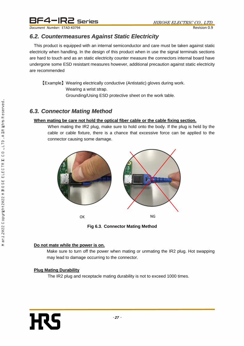
66..33.. CCoonnnneeccttoorr MMaattiinngg MMeetthhoodd
When mating be care not hold the optical fiber cable or the cable fixing section.
When mating the IR2 plug, make sure to hold onto the body. If the plug is held by the
cable or cable fixture, there is a chance that excessive force can be applied to the
connector causing some damage.
Fig 6.3.Connector Mating Method
Do not mate while the power is on.
Make sure to turn off the power when mating or unmating the IR2 plug. Hot swapping
may lead to damage occurring to the connector.
Plug Mating Durability
The IR2 plug and receptacle mating durability is not to exceed 1000 times.
Mar
.1.2
022
Cop
yrig
ht 2
022
HIR
OS
E E
LEC
TR
IC C
O.,
LTD
. All
Rig
hts
Res
erve
d.
HIROSE ELECTRIC CO., LTD. Document Number: ETAD-K0794 Revision 0.9
- 28 -
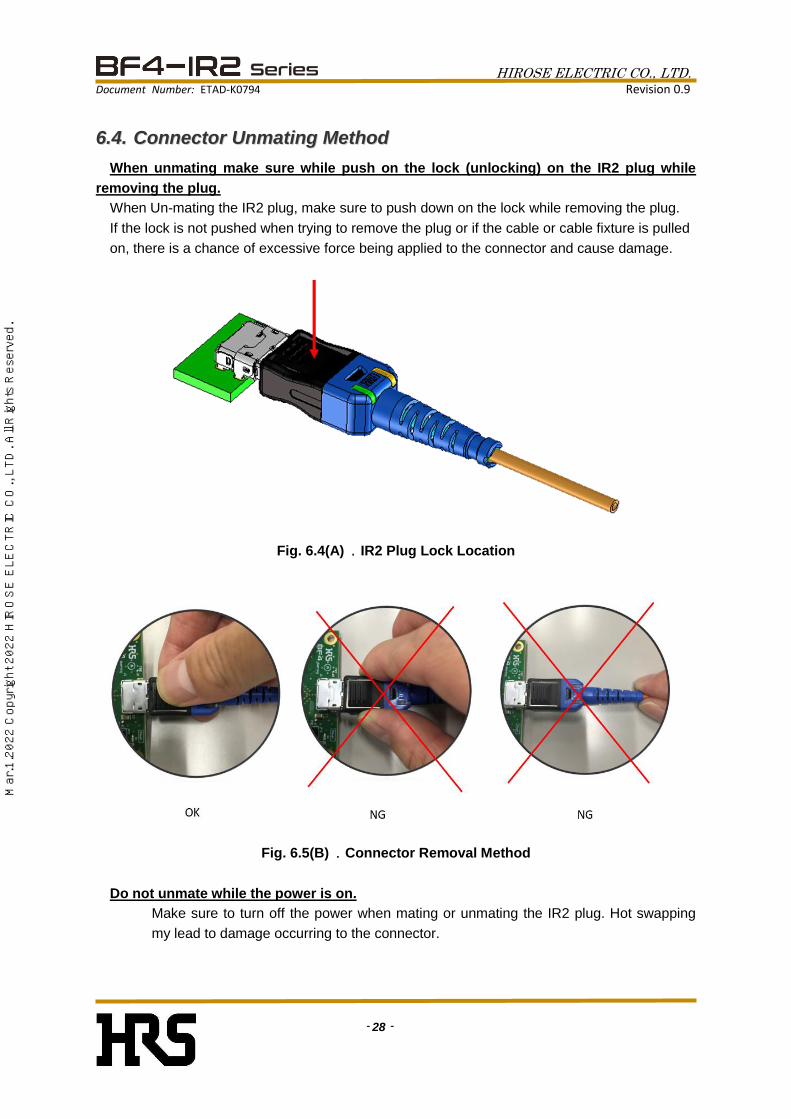
66..44.. CCoonnnneeccttoorr UUnnmmaattiinngg MMeetthhoodd
When unmating make sure while push on the lock (unlocking) on the IR2 plug while
removing the plug.
When Un-mating the IR2 plug, make sure to push down on the lock while removing the plug.
If the lock is not pushed when trying to remove the plug or if the cable or cable fixture is pulled
on, there is a chance of excessive force being applied to the connector and cause damage.
Fig. 6.4(A) .IR2 Plug Lock Location
Fig. 6.5(B) .Connector Removal Method
Do not unmate while the power is on.
Make sure to turn off the power when mating or unmating the IR2 plug. Hot swapping
my lead to damage occurring to the connector.
Mar
.1.2
022
Cop
yrig
ht 2
022
HIR
OS
E E
LEC
TR
IC C
O.,
LTD
. All
Rig
hts
Res
erve
d.
HIROSE ELECTRIC CO., LTD. Document Number: ETAD-K0794 Revision 0.9
- 29 -
66..55.. FFaaiill--ssaaffee ddeessiiggnn
The Product is equipped with a semiconductor for optical-electrical conversion.
Although HRS stands behind the quality and reliability of its products, semiconductor products
have specific characteristics such as the occurrence of failure at a certain rate and malfunctions
under certain use conditions.
Please be sure to implement safety measures to guard them against the possibility of physical
injury, or injury in the event of the failure of a Hirose product, such as safety design including but
not limited to redundancy, malfunction prevention or any other appropriate measures.
In the unlikely event a problem occurs due to the occurrence of failure, we respond appropriately
and promptly after consultation.
Mar
.1.2
022
Cop
yrig
ht 2
022
HIR
OS
E E
LEC
TR
IC C
O.,
LTD
. All
Rig
hts
Res
erve
d.

HIROSE ELECTRIC CO., LTD. Document Number: ETAD-K0794 Revision 0.9
- 30 -
66..66.. NNootteess OOnn HHaannddlliinngg tthhee PPrroodduucctt
(Notes on Change of Information)
・ The content of this document including the information regarding of the connector (Hereafter, The Product) is subject to change without prior notice.
(Prohibition of Reproduction)
・ No part of this document may be copied or reproduced without prior written consent of Hirose Electric Co., LTD. (Hereafter, Hirose). Even if written consent of Hirose is obtained, it is prohibited to amend any part of this document and copy or reproduce it. Hirose shall assume no obligation or liability in connection With such amended information or reproductions.
(Responsibilities for Design Safety)
・ Hirose shall assume no responsibilities for the support for the application of the product or the product design of the customer. The customer shall be responsible for the product and application of the customer in which the product is used. The customer shall take appropriate design and operational safety measures in order to minimize the potential risks predicted for the product and application of the customer in which the product is used.
(Responsibilities for the Determination of Suitability) ・ When using the product, the customer shall ensure safe design at his/her own responsibility so that malfunction or failure
of the product would never cause an infringement on the life, body or property. For design or use of the product, make sure to refer to the materials (including the catalog, specifications, and design note) and follow the same. When using information including the product data provided in the document, technical data or circuit examples shown in the figures and tables, the customer shall evaluate the information on the customer’s product and determine the suitability at the customer’s own responsibility.
(Responsibilities for Specific Applications)
・ Make sure to consult with our sales representative in advance when considering the use of specific applications that require extremely high quality and reliability (I.E. Nuclear Equipment, Aerospace Systems, Transportation Equipment and Various Safety Related Equipment).
(Prohibition of Replication)
・ Do not disassemble, reverse-engineer, modify, analyze or replicate this product.
(Prohibition of the Application of Prohibited Products)
・ The product must not be used for any products that the manufacturing, sale or use is prohibited by domestic or international laws, regulations or ordinances.
(Notes on Guarantee and License)
・ The technical data provided in the materials of the product is intended to describe the representative behaviors and application of the product. It is not to guarantee or license the intellectual property rights or any other rights of Hirose nor a third party.
(Notes on the Warranties for the Contract)
・ Unless otherwise provided in a written contract or other documents (specifications) agreed between the customer and Hirose, Hirose makes no warranties of any kind (Including but not limited to, warranties of the function and operation, warranties of merchantability, warranties of suitability for a specific application or purpose and warranties of correctness of information).
(Prohibition of Weapons of Mass Destruction and Military Purposes)
・ It is prohibited to use the product or the technical information contained in this document for any military purpose, including but not limited to, the development of weapons of mass destruction.
(Notes on Export)
・ To export the product to other countries, the exporter shall conduct the applicability determinations based on the Foreign Exchange and Foreign Trade Act of Japan. If you wish to have the applicability determination sheet issued by Hirose, contact our sales representative. Note that in the export arrangement, the customer shall be an exporter and responsible for compliance with all the applicable laws, regulations, terms and conditions of the agreement with Hirose.
Mar
.1.2
022
Cop
yrig
ht 2
022
HIR
OS
E E
LEC
TR
IC C
O.,
LTD
. All
Rig
hts
Res
erve
d.

HIROSE ELECTRIC CO., LTD. Document Number: ETAD-K0794 Revision 0.9
- 31 -
66..77.. NNootteess oonn tthhee UUssee ooff tthhee PPrroodduucctt
(Notes on the Specification Range)
・ Using the product under conditions beyond the specification range (For voltage, current and temperature) provided in this document may result in an accident (Including ignition, heat generation and smoking). Confirm the document thoroughly and make sure to use the product within the specified range.
(Notes on the Laser Beam)
・ A laser beam is emitted from the end-face of the optical fiber in operation. It may cause eye injuries or loss of sight if it enters the eyes. Do not stare directly into the end-face of the optical fiber. The laser beam is emitted from the VCSEL in operation. It may not be visible depending on its wavelength but none the less it may cause eye injuries or loss of sight if the laser beam or its reflected beam enters the eye. Do not stare (look into) the laser beam directly.
(Notes on the Fracture of the Optical Fiber)
・ In case of the fracture of the optical fiber used in the Product, turn off the power immediately. In addition, use care when handling it to avoid injury from fractured parts or fragments.
(Notes on Use of GaAs)
・ The Product is equipped with a semiconductor within the connector and contains gallium arsenide (GaAs). Vapor and powder of GaAs is harmful to the human body and the environment, please note the following. ・When disposing of the product, the following disposal process is recommended.
・To consign the disposal to a disposer licensed to collect, transport and dispose of materials containing gallium arsenide. ・To separate from general industrial waste and household waste and handle as special industrial waste material until final disposal.
(Notes on Waterproofing)
・ The product is not waterproof and a failure due to condensation or exposure to water is not warranted. If condensation or exposure to water may occur, take appropriate waterproofing measures.
(Notes on Use of Chemicals)
・ Avoid environments where acidic chemicals, alkaline chemicals and organic solvents are present or directly used on the product. The product may deteriorate and affect the features described above.
(Notes on Environment Where Gases are present)
・ Avoid using the product in environments where gasses such as chlorides or sulfides are present. The product may deteriorate and affect the features described above.
(Notes on Storage)
・ Store the product out of range of corrosive substances, corrosive gases, high temperature, humidity and direct sunlight. Do not apply excessive pressure or vibration to the product as it may cause deterioration, deformation, damage or failure of the product.
(Notes on Resin Molding)
・ The resin molding section of the product may contain black sports or the coloring may be slightly different, but this has no effect of the products performance.
Mar
.1.2
022
Cop
yrig
ht 2
022
HIR
OS
E E
LEC
TR
IC C
O.,
LTD
. All
Rig
hts
Res
erve
d.
HIROSE ELECTRIC CO., LTD. Document Number: ETAD-K0794 Revision 0.9
- 32 -
77.. RReevviissiioonn HHiissttoorryy
Table7. Revision history
△ 1
Mar
.1.2
022
Cop
yrig
ht 2
022
HIR
OS
E E
LEC
TR
IC C
O.,
LTD
. All
Rig
hts
Res
erve
d.


